Embed Size (px)
Citation preview
prod
uct n
ote
AN-1298 Agilent EEsof EDA
Generating Custom, Real-World Waveformsfor 3G Wireless Applications

2
Introduction As a system designer, have you ever needed to know the system specifica-tion at the input or output of specific components along the design flow,only to be thwarted by the inability to either measure the specificationthrough instrumentation or simulate the specification with software?Suppose, for example, that you have an ACPR specification for the entiretransmission chain and you want to know the allowable ACPR specificationbefore the input of the power amplifier. The system has been simulated insoftware, you know the simulated ACPR up to the input of the power ampli-fier, and the specific power amplifier has been chosen, but is it the rightpower amplifier for the system? Before continuing on with the design youwant to send the simulated signal, with known ACPR, through the actualpower amplifier to measure at the output of the power amplifier this veryimportant specification.
A few years ago, your only option would have been to continue with thedesign, with no way of knowing whether the system design met the ACPRspecification until after the prototype was fully built and measured. Today,it is possible to integrate the testing of partially completed software andhardware designs by combining the signal simulation capabilities ofAdvanced Design System, EDA software from the Agilent EEsof productgroup with the signal generation capabilities of the Agilent ESG-D seriessignal generator.
In our example, the signal is created in Advanced Design System and sentto the arbitrary waveform generators of the ESG-D to create a real-worldsignal for input into the power amplifier. The ACPR is then measured with avector signal analyzer such as the Agilent 89440 Series Vector SignalAnalyzer (VSA). If the ACPR specification is not met, then the parametersor system components in the transmission chain can be changed to alter theACPR of the signal at the input of the power amplifier. Or, as alternatives, apower amplifier with different ACPR characteristics can be selected or thepower amplifier itself can be modified.
Using our example, other types of system specifications could also be mea-sured, such as Error Vector Magnitude (EVM), Bit Error Rates (BER), andFrame Error Rates (FER) on the receiving chain, and also spur analysis.The signal created by Advanced Design System can also include real-worldimpairments such as multiple scattering noise, IQ offset errors, filter groupdelay, and multipath fading. Using the same signal in the simulation and onthe actual hardware component removes the uncertainties associated withcorrelating measured and modeled results.
Another challenge facing RF and DSP system designers at the forefront oftechnology is to be able to create the needed signal formats and modulationschemes for tomorrow’s standards. Advanced Design System can interfacewith ESG-D to create custom test signals. Linking electronic design automa-tion (EDA) tools with measurement equipment decreases the time neededto evaluate and troubleshoot the system. This link between the design envi-ronment (ADS) and test and measurement environment (ESG-D and VSA)bridges the gap between conceptual design and prototype/test phases.
3
The Advanced Design System/ESG-D link, when used with DesignLibraries from Agilent EEsof EDA, such as W-CDMA, GSM, or cdma-2000-compliant, can greatly reduce your system design time. Features include: • Enabling subsystem evaluation prior to system completion• Allowing measured data to be used in system simulation serving as
flexible waveform generators• Allowing complex and real-world signals to be generated or used in
simulation• Providing precise frequency and level control with modulation using
the HP ESG-D• Creating signals with real-world impairments such as multipath fading
and noise.
This product note describes software and hardware requirements andhow they should be configured for a successful link. These sections include:• An overview of the basic structure of the ADS to ESG-D link • An introduction to Advanced Design System and the ESG-D interface
component • An introduction to the ESG-D signal generator capabilities• An example of W-CDMA and cdma2000 signal generation• A configuration guide for software and hardware components• A list of related literature
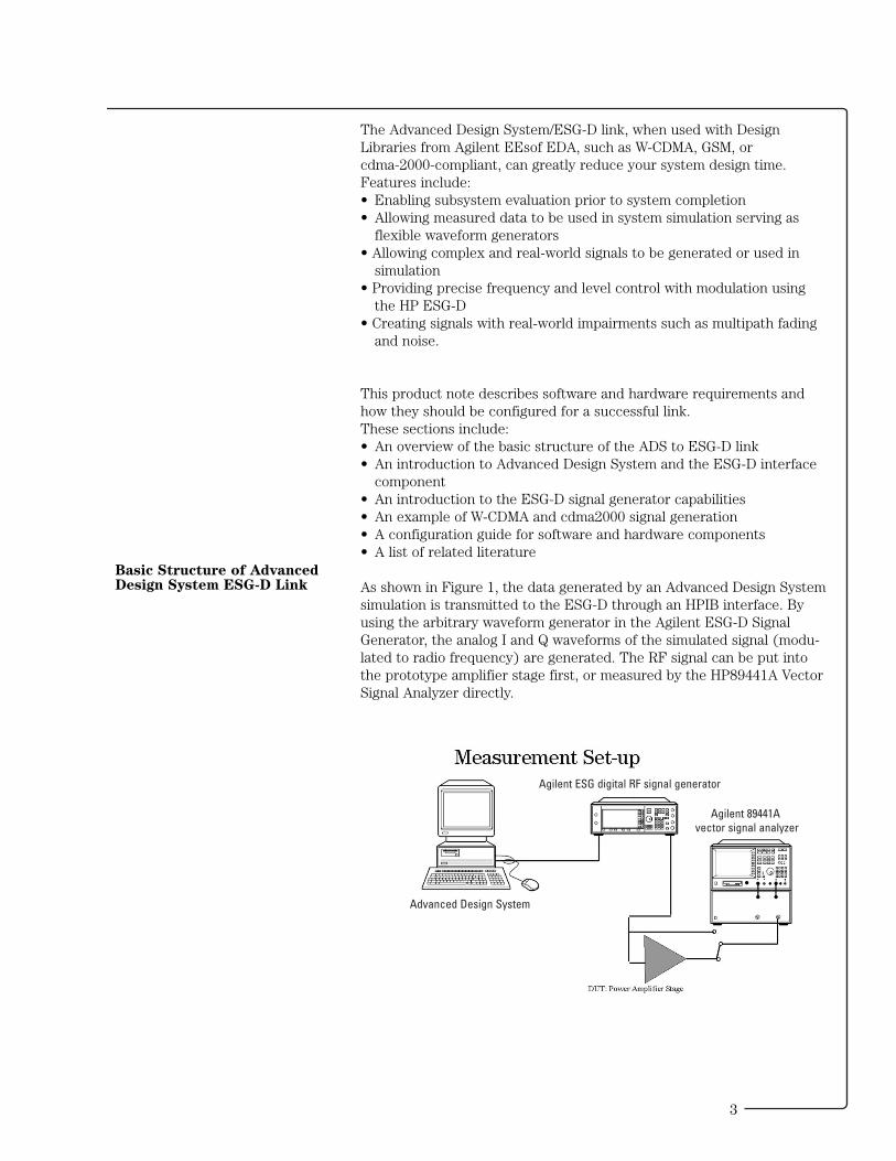
As shown in Figure 1, the data generated by an Advanced Design Systemsimulation is transmitted to the ESG-D through an HPIB interface. Byusing the arbitrary waveform generator in the Agilent ESG-D SignalGenerator, the analog I and Q waveforms of the simulated signal (modu-lated to radio frequency) are generated. The RF signal can be put intothe prototype amplifier stage first, or measured by the HP89441A VectorSignal Analyzer directly.
Basic Structure of AdvancedDesign System ESG-D Link
Agilent ESG digital RF signal generator
Agilent 89441Avector signal analyzer
Advanced Design System

4
This section describes some basics about Advanced Design System thatare relevant to the ESG-D interface. Figure 2 shows the schematic of aQuadrature Amplitude Modulation QAM, scheme. The I and Q bit streamsare transmitted through a 990 MHz modulator and demodulator. Thedemodulated/received signal at the demodulator output is automaticallydownloaded to the ESG-D instrument immediately after the ESGInterfacecomponent has collected all the required data. The transmitted signal atthe modulator input could also have been downloaded to the ESG-Dinstrument. The ESGInterface component will collect the desired seg-ment of a time domain signal, download the time-limited simulation datato the ESG-D instrument, and set all the necessary controls and parame-ters of the ESG-D instrument. Some important component parameters onthe ESGInterface component include:
• DataRate, to set the desired data transmission rate• NsamplesPerInputSym, to set the number of simulation points per
input symbol• Tstep to set the simulation time step
As the Dual Arbitrary Waveform Generator module of the ESG acceptsonly a finite number of data points, the downloaded signal becomes atime-limited signal. In general, a time-limited signal cannot be bandlimit-ed. There will always be frequency spectrum overlap between repeatingfrequency spectrum sections of the sampled version of the original time-limited time-domain signal. Even with the use of an ideal lowpass filter,some unwanted high-frequency components, of aliasing errors, will bepresent in the reproduced physical signal.
Advanced DesignSystem Basics
Using the ESG-D in the Schematic

5
This effect can be minimized by using a Repeat component (NumTimes=3)in front of the ESG to provide end-point signal continuity (see Figure 3).The filtered and downloaded data to the ESG is the middle third of thegenerated data. The ESGInterface Start parameter must also consider thefilter length (number of taps and interpolation or decimation parameters)so that only the steady-state filter output is taken by ESGInterface.
For example, in Wideband Code Division Multiple Access (W-CDMA) witha chip rate of 3.84 MHz and 10 msec of information (one traffic frame) ofinterest, the Repeat component output is connected to a FIR filter that has200taps with an upsample and interpolation value of 4. The FIR filter out-put is connected to the ESGInterface component.
BlockSize of Repeat = (2.84 x MHz) x (10 msec) = 38400 samples
Start of ESGInterface= Interpolation of FIR x (BlockSize of Repeat + #FIR taps +1)= 4 x (38400 + 200 + 1) = 154404
Stop of ESGInterface= 2 x Interpolation of FIR x (BlockSIze of Repeat + #FIR taps +1)= 2 x 4 x (38400 + 200 + 1) = 308808
Repeat Filter ESGInterface

6
Electronic Signal Generator InterfaceESGInterface
Parameters:Interface = name of HPIB / GPIB interface or IP addressAddress = address of ESG on interfaceStart = sample to start waveform recording specify when to start and stop data collection. The number of samples
collected, Stop - Start + 1, must be in the range 16 to 1,048,576. The ESG requires an even number of samples;the last sample will be discarded if Stop - Start + 1 is odd.
Stop = sample to stop waveform recordingFrequency = RF output frequencyAmplitude = RF output power levelARB_Ref = waveform clock reference option:
The ARB_Ref parameter specifies an internal or external reference for the ESG clock generator. If set to External, the ARB_RefFreq parameter sets the frequency of this clock. Acceptable values range from 250 kHz to 20 MHz. Internal or External
ARB_RefFreq = reference frequency for the external clock generatorRecFilter = reconstruction filter between DAC output and ESG output: through (no filtering), filter_250kHz,
filter_2500kHz, filter_8MHz. The RecFilter parameter specifies the cutoff frequency for the reconstruction filter that lies between the DAC output and the Dual Arbitrary Waveform Generator output inside the ESG.
SampleClk = sample clock rate for sequencer and DAC converterrange from 1 Hz to 40 MHz.
FileName = waveform file name to be stored in ESGInputScaling = specifies whether to scale inputs. If set to active, inputs are scaled to +/- ScalingFactor; if set to inactive,
any data with an absolute magnitude larger than 1V will be interpreted as 1V. In general, use only a frac-tion of the full scale (set ScalingFactor <<1V) for better adjacent channel power ratio performance. Driving the I/Q modulator of the Dual Arbitrary Waveform Generator at the 1V maximum level can cause non-linear distortion leading to spectral regrowth.
ScalingFactor = input scaling factorSignalFilter = parameter is used to select a root raised cosine filter that will filter data before it is sent to the ESG.
The filter options are for W-CDMA signals at specified chip rates and include compensation for appropriate ESG reconstruction filter and D/A sin(x)/x roll-off. The WCDMA 4096 MHz Chiprate option is for signals that have a chip rate of 4096 MHz and 4 samples per symbol. The internal FIR filter has 200 tap coefficients. Set the RecFilter option to 2500 kHz when using this filter. The WCDMA 8192 MHz Chiprate option is for signals that have a chip rate of 8192 MHz and 4 samples per symbol. The internal FIR filter has 112 tap coefficients. Set the RecFilter option to 8 MHz when using this filter. The WCDMA 16384 MHz Chiprate option is for signals that have a chiprate of 16384 MHz and 2 samples per symbol. The internal FIR filter has 64 tap coefficients. Set the RecFilter option to 8 MHz when using this filter. The ESG can sense when the signal has less than 4 samples per symbol and apply sin(x)/x compensation for the D/A automatically. These tap coefficients thus do not include this compensation.
DataWindowing = type of input windowing:Hamming, pseudoRectangular, threePtAverage, Hann, or Blackman
EventMarkers = The EventMarkers parameter specifies which ESG Event markers are enabled: Event1, Event2, Both, or Neither. Event markers are useful for synchronizing other instruments to the ESG. Refer to the HPESG-D Series Options UND and UN5 Signal Generators manual, Chapter 2, for more information.
ARB_On = turn ESG on immediately after data is downloaded:manual or automatic
Range of Usage: 16 < Stop - Start + 1 > 1,048,576 (or less, if limited by available RAM in ESG) 250 kHz < ARB_RefFreq > 20 MHz1 Hz < SampleClk £> 40 MHzScalingFactor > 1
Inputs:I = I (real) part of a quadrature input (signal type: floating point)Q = Q (imaginary) part of a quadrature input (signal type: floating point)
I and Q must be of equal length.

7
The Agilent ESG-D Series of RF signal generators with option UND, dualaribitrary waveform generator, provides extremely flexible baseband gen-eration for the most complex RF waveforms. With the capability to drivethe ESG-D’s I/Q modulator, the internal dual arbitrary waveform genera-tor provides the power to simulate complex, nonstandard or proprietarymodulated RF signals. These modulated waveforms are easily generatedwith Advanced Design System software.
The ESG-D series with Option UND provides users the flexibility to cre-ate completely arbitrary I/Q waveforms. Using ADS to generate I and Qwaveforms externally, the ESG-D can be expanded to include the follow-ing applications:
• Simulating digitally modulated signals with up to 20 MHz bandwidth• Generating two or more CW tones with one HP ESG-D• Generating multichannel and multicarrier signals such as orthogonal
frequency division multiplexing (OFDM). • Generating a signal that includes noise or other impairments• Creating multiple modulated RF carriers, such as mixed NADC and
CDMA carriers for base-station amplifer testing
• Dedicated physical channels (DTCH) with multiple symbol rate• Perch channel • Soft quadrature phase shift keying (QPSK) modulation• Orthogonal multiple spreading factors (SF) codes in forward link• Long random sequence with chip rate of 4.096 Mcps• Radio frequency (RF) with 2 GHz in PCS band• W-CDMA spectrum with bandwidth of 5MHz• FIR filter designed by HP Microwave Instrument Division used in
transmission• Signal wrapped around before transmission• Power of each channel adjusted independently• An IMT2000 channel is applied after the transmit filter
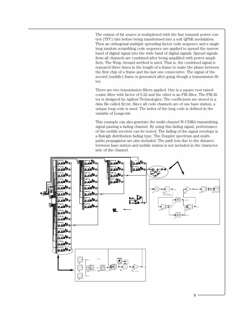
This example generates the W-CDMA transmitting signal with bandwidthof 5MHz at carrier frequency band of 2 GHz for code domain measure-ment in W-CDMA-ESG link testing. The design itself generates the multi-channel W-CDMA transmitting signal passing a fading channel. By usingthis fading signal, performance of the mobile receiver can be tested. Thefading of the signal envelope is a Raleigh distribution fading type. TheDoppler spectrum and multi-paths propagation are also included. Thepath loss due to the distance between base station and mobile station isnot included in the characteristic of the channel.
The 29 code channels include:• A Perch channel spread with short code C8(0)• Fifteen 32ksps dedicated physical channels (DTCH) spread with short
codes C7(1) to C7(15)• Eight 64ksps DTCHs spread with code C6(16) to C6(23)• Four 12 ksps DTCHs spread with code C5(16) to C5(19) and two
256ksps DTCHs spread with code C4(12) and C4(13)
None of the 29 DTCHs consist of channel encoder. Random bit streamsource components are used as the framed and channel-coded data.
Agilent ESG-D SeriesSignal Generator Basics
Example 1Multi-Channel with
Fading Channel in Forward
Link
Example Design Name:
MultiChannel_fading.dsn
Features:
Description
8
The output of bit source is multiplexed with the fast transmit power con-trol (TPC) bits before being transformed into a soft QPSK modulation.Then an orthogonal multiple spreading factor code sequence and a singlelong random scrambling code sequence are applied to spread the narrowband of digital signal into the wide band of digital signals. Spread signalsfrom all channels are combined after being amplified with power ampli-fiers. The Wrap Around method is used. That is, the combined signal isrepeated three times in the length of a frame to make the phase betweenthe first chip of a frame and the last one consecutive. The signal of thesecond (middle) frame is generated after going though a transmission fil-ter.
There are two transmission filters applied. One is a square root raisedcosine filter with factor of 0.22 and the other is an FIR filter. The FIR fil-ter is designed by Agilent Technologies. The coefficients are stored in adata file called fir.txt. Since all code channels are of one base station, aunique long code is used. The index of the long code is defined in thevariable of Longcode.
This example can also generate the multi-channel W-CDMA transmittingsignal passing a fading channel. By using this fading signal, performanceof the mobile receiver can be tested. The fading of the signal envelope isa Raleigh distribution fading type. The Doppler spectrum and multi-paths propagation are also included. The path loss due to the distancebetween base station and mobile station is not included in the character-istic of the channel.
9
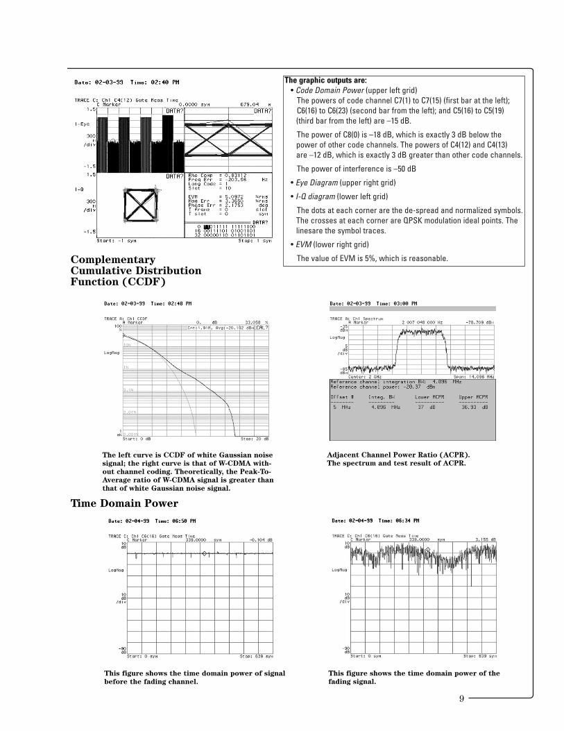
ComplementaryCumulative DistributionFunction (CCDF)
Time Domain Power
The graphic outputs are:• Code Domain Power (upper left grid)
The powers of code channel C7(1) to C7(15) (first bar at the left); C6(16) to C6(23) (second bar from the left); and C5(16) to C5(19) (third bar from the left) are –15 dB.
The power of C8(0) is –18 dB, which is exactly 3 dB below the power of other code channels. The powers of C4(12) and C4(13) are –12 dB, which is exactly 3 dB greater than other code channels.
The power of interference is –50 dB
• Eye Diagram (upper right grid)
• I-Q diagram (lower left grid)
The dots at each corner are the de-spread and normalized symbols.The crosses at each corner are QPSK modulation ideal points. The linesare the symbol traces.
• EVM (lower right grid)
The value of EVM is 5%, which is reasonable.
This figure shows the time domain power of signal
before the fading channel.
This figure shows the time domain power of the
fading signal.
Adjacent Channel Power Ratio (ACPR).
The spectrum and test result of ACPR.
The left curve is CCDF of white Gaussian noise
signal; the right curve is that of W-CDMA with-
out channel coding. Theoretically, the Peak-To-
Average ratio of W-CDMA signal is greater than
that of white Gaussian noise signal.

10
• 5 channels (Pilot, Fundamental, Supplemental1, Supplemental2 and Dedicated Control channels)
• Orthogonal Walsh code spreading • HPSK modulation• Masked long PN code used to distinguish mobiles • FIR filters for SR1 and SR3 respectively according to cdma2000 standard
This example generates the cdma2000 transmitting signal in reverse linkfor ESG link testing. The power level of the R-FCH is about 7.5dB belowthe power level of the R-Pilot. On pilot channel, a power control group isdivided into 4 blocks and Pilot signal (all ‘0’ s) occupy the first three blocksand the power control bits occupy the last one. For other channels, ran-dom bit sources are used as the signal sources. Data on Fundamental andDedicated Control Channels are spread by 16-bits Walsh codes, and onSupplemental channels are spread by 8-bits Walsh codes, then HPSK mod-ulated with PN codes. The final chip rates are 1.2288Mcps and 3.6864Mcpsrespectively for SR1 and SR3.The spread and modulated signal is passed through a FIR filter beforeinput into the ESGInterface component.
Schematic
• Multiple channels(Subnetwork: HPSKChannel)
Example 2Five channels in Reverse Link
without Channel Coding
Design Name:
EsgCDMA_RevSR1Hpsk.dsn
Features:
Description
Test Results
CCDF ACPR

111. Requires Advanced Design System release 1.3
Configuration GuideDesign Tools RequirementsAdvanced Design System Required Suites (Select at least one)• DSP Designer Pro (Agilent E8821A/AN)• Communications System Designer Pro (Agilent E8851A/AN)• Communications System Designer Premier (Agilent E8852A/AN)Required Options (depending on applications)• W-CDMA design llibrary (Agilent E8855A/AN)• CDMA design library (Agilent E8857A/AN)• CDMA2000-Compliant Design Library (Agilent E8877A/AN)Platform and Interface Requirements• HP B/C/J - Class Workstations
HPUX 10.2 LAN/HPIB HP E2050APCI HP E2078AISA/EISA HP E2071DISA/EISA National Instruments GPIB-HP700-EISA
HPUX 11.0 LAN/HPIB HP E2050A1
• SUN MicrosystemsSolaris 2.5, 2.6 LAN/HPIB HP E2050A1
SBus National Instruments GPIB-SPRC-BPCI National Instruments PCI-GPIB Sun SPARCstation
• Windows NTNT 4.0 LAN/HPIB HP E2050A
ISA/EISA HP 82341C/DPCI National Instruments PCI-GPIB for Windows NTPCMCIA National Instruments PCMCIA-GPIB for Win NTEISA/ISA/AT National Instruments AT-GPIB/TNT for Win NT
• Windows 98/95 LAN/HPIB HP E2050AISA/EISA HP 82341C/DPCI National Instruments PCI-GPIB for Windows 98/95PCMCIA National Instruments PCMCIA-GPIB for Win 98/95EISA/ISA/AT National Instruments AT-GPIB/TNT for Win 98/95
Test EquipmentAgilent ESG-D and ESG-DP series digital RF signal generator (Select at least one)• Agilent E4432B 3 GHz digital RF signal generator• Agilent E4433B 4 GHz digital RF signal generator• Agilent E4436B 3 GHz digital RF signal generator with high spectral purity• Agilent E4437B 4 GHz digital RF signal generator with high spectral purityRequired Options• Option UND internal dual arbitrary waveform generator• Option 1E5 high-stability timebaseRecommended Options• Option UN8 real-time I/Q baseband generator with TDMA standards and 1M RAM• Option UN5 multicarrier, multichannel CDMA personality• Option 100 multichannel W-CDMA personality• Option 101 multichannel cdma2000 personality• Option 202 EDGE personality• Option H99 improved ACP performance for TETRA,CDMA, and WCDMAHP 89400 series vector signal analyzer• Agilent 89441A vector signal analyzerRequired Options• Option B73 W-CDMA code domain power measurements • Option AY9 extended time capture• Option AYA vector modulation analysis • Option UTH 20 Mbytes extended RAMRecommended Options• Option AYJ adaptive equalization to AYA• Option XXX ARIB 1.0-1.2 or 3GPP W-CDMA (Available x/x/xx) • Option XXX EDGE (Available x/x/xx)
12
For more information about Agilent
Technologies test and measurement
products, applications, services, and
for a current sales office listing, visit
our web site:
http://www.agilent.com/find/tmdir
You can also contact one of the fol-
lowing centers and ask for a test and
measurement sales representative.
United States:
Agilent Technologies Test and Measurement Call CenterP.O. Box 4026Englewood, CO 80155-4026 (tel) 1 800 452 4844
Canada:
Agilent Technologies Canada Inc.5150 Spectrum WayMississauga, Ontario, L4W 5G1(tel) 1 877 894 4414
Europe:
Agilent TechnologiesEuropean Marketing OrganizationP.O. Box 9991180 AZ AmstelveenThe Netherlands(tel) (31 20) 547 9999
Japan:
Agilent Technologies Japan Ltd.Measurement Assistance Center9-1, Takakura-Cho, Hachioji-Shi,Tokyo 192-8510, Japan(tel) (81) 426 56 7832(fax) (81) 426 56 7840
Latin America:
Agilent TechnologiesLatin American Region Headquarters5200 Blue Lagoon Drive, Suite #950Miami, Florida 33126, U.S.A.(tel) (305) 267 4245(fax) (305) 267 4286
Australia/New Zealand:
Agilent Technologies Australia Pty Ltd 347 Burwood HighwayForest Hill, Victoria 3131
(tel) 1-800 629 485 (Australia)(fax) (61 3) 9272 0749(tel) 0 800 738 378 (New Zealand)(fax) (64 4) 802 6881
Asia Pacific:
Agilent Technologies19/F, Cityplaza One, 1111 King’s Road,Taikoo Shing, Hong Kong, SAR(tel) (852) 2599 7889(fax) (852) 2506 9233
http://www.agilent.com/eesof-eda
Technical data is subject to change
Copyright © 1999
Agilent Technologies
Printed in U.S.A. 11/99
5968-8388E
Literature• Technical brief,“Connected Solutions for 3G,”
literature number 5968-5031E.• Product note, “A Flexible Waveform Generator Using OmniSys and
Instrumentation,” (describes how to create baseband signals using HP Eesof’s SeriesIV Omnisys software and the HP1445 Arbitrary Function Generator), literature number E4600-9.
• Brochure, “HP ESG Series RF Signal Generators,” literature number 5968-4313E.
• “Profile of options for the HP ESG family,” literature number 5968-2807E.
• “Configuration guide,” literature number 5965-4973E.
• “Technical specifications,”literature number 5965-3096E.
• Product note, “Generating and Downloading Data to the ESG-D RF
Signal Generator for Digital Modulation,” literature number 5966-1010E.
• Product note, “Generating Digital Modulation with the ESG-D Series
dual Arbitrary Waveform Generator,” literature number 5966-4097E.
• Product note, “Customize Digital Modulation with the HP ESG-D
Series Real-Time I/Q Baseband Generator,” literature number 5966-4096E.
• Brochure, “CDMA Solutions from HP,” literature number 5966-3058E.
• Brochure, “GSM Solutions from HP,” literature number 5966-1550E
• Brochure, “WCDMA Solutions from HP,” literature number 5967-6349E.
• CD-ROM, “W-CDMA Solutions from HP, Workshop ’98,” literature number E8900-10025.
• Brochure, “HP Communications Systems Designer,” literature number 5966-0670E.