Embed Size (px)
Citation preview

Ramon Pallas-Areny. "Amplifiers and Signal Conditioners."
Copyright 2000 CRC Press LLC. <http://www.engnetbase.com>.
Amplifiers andSignal Conditioners
80.1 Introduction80.2 Dynamic Range80.3 Signal Classification
Single-Ended and Differential Signals • Narrowband and Broadband Signals • Low- and High-Output-Impedance Signals
80.4 General Amplifier Parameters80.5 Instrumentation Amplifiers
Instrumentation Amplifiers Built from Discrete Parts • Composite Instrumentation Amplifiers
80.6 Single-Ended Signal Conditioners80.7 Carrier Amplifiers80.8 Lock-In Amplifiers80.9 Isolation Amplifiers80.10 Nonlinear Signal-Processing Techniques
Limiting and Clipping • Logarithmic Amplification • Multiplication and Division
80.11 Analog Linearization80.12 Special-Purpose Signal Conditioners
80.1 Introduction
Signals from sensors do not usually have suitable characteristics for display, recording, transmission, orfurther processing. For example, they may lack the amplitude, power, level, or bandwidth required, orthey may carry superimposed interference that masks the desired information.
Signal conditioners, including amplifiers, adapt sensor signals to the requirements of the receiver(circuit or equipment) to which they are to be connected. The functions to be performed by the signalconditioner derive from the nature of both the signal and the receiver. Commonly, the receiver requiresa single-ended, low-frequency (dc) voltage with low output impedance and amplitude range close to itspower-supply voltage(s). A typical receiver here is an analog-to-digital converter (ADC).
Signals from sensors can be analog or digital. Digital signals come from position encoders, switches,or oscillator-based sensors connected to frequency counters. The amplitude for digital signals must becompatible with logic levels for the digital receiver, and their edges must be fast enough to prevent anyfalse triggering. Large voltages can be attenuated by a voltage divider and slow edges can be acceleratedby a Schmitt trigger.
Analog sensors are either self-generating or modulating. Self-generating sensors yield a voltage (ther-mocouples, photovoltaic, and electrochemical sensors) or current (piezo- and pyroelectric sensors) whose
Ramón Pallás-ArenyUniversitat Politècnica de Catalunya
© 1999 by CRC Press LLC
bandwidth equals that of the measurand. Modulating sensors yield a variation in resistance, capacitance,self-inductance or mutual inductance, or other electrical quantities. Modulating sensors need to be excitedor biased (semiconductor junction-based sensors) in order to provide an output voltage or current.Impedance variation-based sensors are normally placed in voltage dividers, or in Wheatstone bridges(resistive sensors) or ac bridges (resistive and reactance-variation sensors). The bandwidth for signalsfrom modulating sensors equals that of the measured in dc-excited or biased sensors, and is twice thatof the measurand in ac-excited sensors (sidebands about the carrier frequency) (see Chapter 81). Capac-itive and inductive sensors require an ac excitation, whose frequency must be at least ten times higherthan the maximal frequency variation of the measurand. Pallás-Areny and Webster [1] give the equivalentcircuit for different sensors and analyze their interface.
Current signals can be converted into voltage signals by inserting a series resistor into the circuit.Graeme [2] analyzes current-to-voltage converters for photodiodes, applicable to other sources. Hence-forth, we will refer to voltage signals to analyze transformations to be performed by signal conditioners.
80.2 Dynamic Range
The dynamic range for a measurand is the quotient between the measurement range and the desiredresolution. Any stage for processing the signal form a sensor must have a dynamic range equal to or largerthan that of the measurand. For example, to measure a temperature from 0 to 100°C with 0.1°C resolution,we need a dynamic range of at least (100 – 0)/0.1 = 1000 (60 dB). Hence a 10-bit ADC should be appropriateto digitize the signal because 210 = 1024. Let us assume we have a 10-bit ADC whose input range is 0 to 10V; its resolution will be 10 V/1024 = 9.8 mV. If the sensor sensitivity is 10 mV/°C and we connect it to theADC, the 9.8 mV resolution for the ADC will result in a 9.8 mV/(10 mV/°C) = 0.98°C resolution! In spiteof having the suitable dynamic range, we do not achieve the desired resolution in temperature because theoutput range of our sensor (0 to 1 V) does not match the input range for the ADC (0 to 10 V).
The basic function of voltage amplifiers is to amplify the input signal so that its output extends acrossthe input range of the subsequent stage. In the above example, an amplifier with a gain of 10 wouldmatch the sensor output range to the ADC input range. In addition, the output of the amplifier shoulddepend only on the input signal, and the signal source should not be disturbed when connecting theamplifier. These requirements can be fulfilled by choosing the appropriate amplifier depending on thecharacteristics of the input signal.
80.3 Signal Classification
Signals can be classified according to their amplitude level, the relationship between their source terminalsand ground, their bandwidth, and the value of their output impedance. Signals lower than around 100 mVare considered to be low level and need amplification. Larger signals may also need amplificationdepending on the input range of the receiver.
Single-Ended and Differential Signals
A single-ended signal source has one of its two output terminals at a constant voltage. For example,Figure 80.1a shows a voltage divider whose terminal L remains at the power-supply reference voltageregardless of the sensor resistance, as shown in Figure 80.1b. If terminal L is at ground potential (groundedpower supply in Figure 80.1a), then the signal is single ended and grounded. If terminal L is isolatedfrom ground (for example, if the power supply is a battery), then the signal is single ended and floating.If terminal L is at a constant voltage with respect to ground, then the signal is single ended and drivenoff ground. The voltage at terminal H will be the sum of the signal plus the off-ground voltage. Therefore,the off-ground voltage is common to H and L; hence, it is called the common-mode voltage. For example,a thermocouple bonded to a power transistor provides a signal whose amplitude depends on the tem-perature of the transistor case, riding on a common-mode voltage equal to the case voltage.
© 1999 by CRC Press LLC
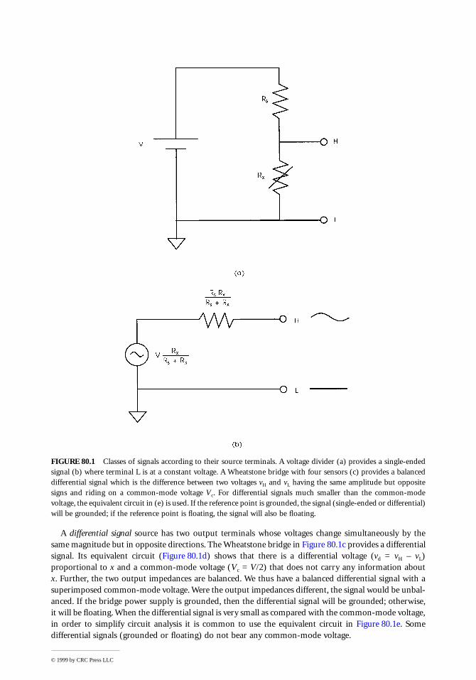
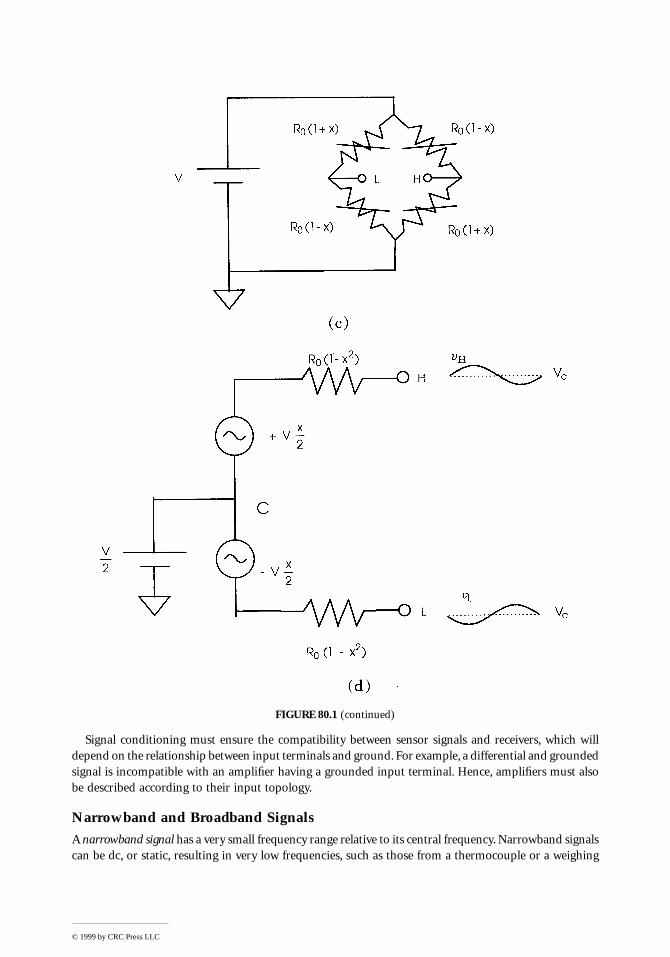
A differential signal source has two output terminals whose voltages change simultaneously by thesame magnitude but in opposite directions. The Wheatstone bridge in Figure 80.1c provides a differentialsignal. Its equivalent circuit (Figure 80.1d) shows that there is a differential voltage (vd = vH – vL)proportional to x and a common-mode voltage (Vc = V/2) that does not carry any information aboutx. Further, the two output impedances are balanced. We thus have a balanced differential signal with asuperimposed common-mode voltage. Were the output impedances different, the signal would be unbal-anced. If the bridge power supply is grounded, then the differential signal will be grounded; otherwise,it will be floating. When the differential signal is very small as compared with the common-mode voltage,in order to simplify circuit analysis it is common to use the equivalent circuit in Figure 80.1e. Somedifferential signals (grounded or floating) do not bear any common-mode voltage.
FIGURE 80.1 Classes of signals according to their source terminals. A voltage divider (a) provides a single-endedsignal (b) where terminal L is at a constant voltage. A Wheatstone bridge with four sensors (c) provides a balanceddifferential signal which is the difference between two voltages vH and vL having the same amplitude but oppositesigns and riding on a common-mode voltage Vc. For differential signals much smaller than the common-modevoltage, the equivalent circuit in (e) is used. If the reference point is grounded, the signal (single-ended or differential)will be grounded; if the reference point is floating, the signal will also be floating.
© 1999 by CRC Press LLC
Signal conditioning must ensure the compatibility between sensor signals and receivers, which willdepend on the relationship between input terminals and ground. For example, a differential and groundedsignal is incompatible with an amplifier having a grounded input terminal. Hence, amplifiers must alsobe described according to their input topology.
Narrowband and Broadband SignalsA narrowband signal has a very small frequency range relative to its central frequency. Narrowband signalscan be dc, or static, resulting in very low frequencies, such as those from a thermocouple or a weighing
FIGURE 80.1 (continued)
© 1999 by CRC Press LLC
scale, or ac, such as those from an ac-driven modulating sensor, in which case the exciting frequency(carrier) becomes the central frequency (see Chapter 81).
Broadband signals, such as those from sound and vibration sensors, have a large frequency rangerelative to their central frequency. Therefore, the value of the central frequency is crucial; a signal rangingfrom 1 Hz to 10 kHz is a broadband instrumentation signal, but two 10 kHz sidebands around 1 MHzare considered to be a narrowband signal. Signal conditioning of ac narrowband signals is easier becausethe conditioner performance only needs to be guaranteed with regard to the carrier frequency.
Low- and High-Output-Impedance Signals
The output impedance of signals determines the requirements of the input impedance of the signalconditioner. Figure 80.2a shows a voltage signal connected to a device whose input impedance is Zd. Thevoltage detected will be
(80.1)
Therefore, the voltage detected will equal the signal voltage only when Zd >> Zs; otherwise vd ¹ vs andthere will be a loading effect. Furthermore, it may happen that a low Zd disturbs the sensor, changing thevalue of vs and rendering the measurement useless or, worse still, damaging the sensor.
At low frequencies, it is relatively easy to achieve large input impedances even for high-output-impedance signals, such as those from piezoelectric sensors. At high frequencies, however, stray inputcapacitances make it more difficult. For narrowband signals this is not a problem because the value forZs and Zd will be almost constant and any attenuation because of a loading effect can be taken intoaccount later. However, if the impedance seen by broadband signals is frequency dependent, then eachfrequency signal undergoes different attenuations which are impossible to compensate for.
Signals with very high output impedance are better modeled as current sources, Figure 80.2b. Thecurrent through the detector will be
FIGURE 80.1 (continued)
v vZ
Z Zd sd
d s
=+
© 1999 by CRC Press LLC

(80.2)
In order for id = is, it is required that Zd << Zs which is easier to achieve than Zd >> Zs. If Zd is not lowenough, then there is a shunting effect.
80.4 General Amplifier Parameters
A voltage amplifier produces an output voltage which is a proportional reproduction of the voltagedifference at its input terminals, regardless of any common-mode voltage and without loading the voltagesource. Figure 80.3a shows the equivalent circuit for a general (differential) amplifier. If one input terminalis connected to one output terminal as in Figure 80.3b, the amplifier is single ended; if this commonterminal is grounded, the amplifier is single ended and grounded; if the common terminal is isolatedfrom ground, the amplifier is single ended and floating. In any case, the output power comes from thepower supply, and the input signal only controls the shape of the output signal, whose amplitude isdetermined by the amplifier gain, defined as
FIGURE 80.2 Equivalent circuit for a voltage signal connected to a voltage detector (a) and for a current signalconnected to a current detector (b). We require Zd >> Zo in (a) to prevent any loading effect, and Zd << Zs in (b)to prevent any shunting effect.
i iZ
Z Zd ss
d s
=+
© 1999 by CRC Press LLC
FIGURE 80.3 General amplifier, differential (a) or single ended (b). The input voltage controls the amplitude ofthe output voltage, whose power comes from the power supply.
© 1999 by CRC Press LLC

(80.3)
The ideal amplifier would have any required gain for all signal frequencies. A practical amplifier has again that rolls off at high frequency because of parasitic capacitances. In order to reduce noise and rejectinterference, it is common to add reactive components to reduce the gain for out-of-band frequenciesfurther. If the gain decreases by n times 10 when the frequency increases by 10, we say that the gain(downward) slope is 20n dB/decade. The corner (or –3 dB) frequency f0 for the amplifier is that for whichthe gain is 70% of that in the bandpass. (Note: 20 log 0.7 = –3 dB). The gain error at f0 is then 30%,which is too large for many applications. If a maximal error e is accepted at a given frequency f, then thecorner frequency for the amplifier should be
(80.4)
For example, e = 0.01 requires f0 = 7f, e = 0.001 requires f0 = 22.4f. A broadband signal with frequencycomponents larger than f would undergo amplitude distortion. A narrowband signal centered on afrequency larger than f would be amplified by a gain lower than expected, but if the actual gain ismeasured, the gain error can later be corrected.
Whenever the gain decreases, the output signal is delayed with respect to the output. In the aboveamplifier, an input sine wave of frequency f0 will result in an output sine wave delayed by 45° (and withrelative attenuation 30% as compared with a sine wave of frequency f >> f0). Complex waveforms havingfrequency components close to f0 would undergo shape (or phase) distortion. In order for a waveformto be faithfully reproduced at the output, the phase delay should be either zero or proportional to thefrequency (linear phase shift). This last requirement is difficult to meet. Hence, for broadband signals itis common to design amplifiers whose bandwidth is larger than the maximal input frequency. Narrow-band signals undergo a delay which can be measured and corrected.
An ideal amplifier would have infinite input impedance. Then no input current would flow whenconnecting the signal, Figure 80.2a, and no energy would be taken from the signal source, which wouldremain undisturbed. A practical amplifier, however, will have a finite, yet large, input impedance at lowfrequencies, decreasing at larger frequencies because of stray input capacitances. If sensors are connectedto conditioners by coaxial cables with grounded shields, then the capacitance to ground can be very large(from 70 to 100 pF/m depending on the cable diameter). This capacitance can be reduced by using drivenshields (or guards) (see Chapter 89). If twisted pairs are used instead, the capacitance between wires isonly about 5 to 8 pF/m, but there is an increased risk of capacitive interference.
Signal conditioners connected to remote sensors must be protected by limiting both voltage and inputcurrents. Current can be limited by inserting a power resistor (100 W to 1 kW , 1 W for example), a PTCresistor or a fuse between each signal source lead and conditioner input. Input voltages can be limitedby connecting diodes, zeners, metal-oxide varistors, gas-discharge devices, or other surge-suppressionnonlinear devices, from each input line to dc power-supply lines or to ground, depending on the particularprotecting device. Some commercial voltage limiters are Thyzorb® and Transzorb® (General Semicon-ductor), Transil® and Trisil® (SGS-Thomson), SIOV® (Siemens), and TL7726 (Texas Instruments).
The ideal amplifier would also have zero output impedance. This would imply no loading effect becauseof a possible finite input impedance for the following stage, low output noise, and unlimited outputpower. Practical amplifiers can indeed have a low output impedance and low noise, but their outputpower is very limited. Common signal amplifiers provide at best about 40 mA output current andsometimes only 10 mA. The power gain, however, is quite noticeable, as input currents can be in thepicoampere range (10–12 A) and input voltages in the millivolt range (10–3 V); a 10 V, 10 mA outputwould mean a power gain of 1014! Yet the output power available is very small (100 mW). Power amplifiers
Gv
v= o
d
ff f
0 =-( )-
»1
2 22
e
e e e
© 1999 by CRC Press LLC

are quite the opposite; they have a relatively small power gain but provide a high-power output. For bothsignal and power amplifiers, output power comes from the power supply, not from the input signal.
Some sensor signals do not require amplification but only impedance transformation, for example, tomatch their output impedance to that of a transmission line. Amplifiers for impedance transformation(or matching) and G = 1 are called buffers.
80.5 Instrumentation Amplifiers
For instrumentation signals, the so-called instrumentation amplifier (IA) offers performance closest tothe ideal amplifier, at a moderate cost (from $1.50 up). Figure 80.4a shows the symbol for the IA andFigure 80.4b its input/output relationship; ideally this is a straight line with slope G and passing throughthe point (0,0), but actually it is an off-zero, seemingly straight line, whose slope is somewhat differentfrom G. The output voltage is
(80.5)
where va depends on the input voltage vd, the second term includes offset, drift, noise, and interference-rejection errors, G is the designed gain, and vref is the reference voltage, commonly 0 V (but not necessarily,thus allowing output level shifting). Equation 80.5 describes a worst-case situation where absolute valuesfor error sources are added. In practice, some cancellation between different error sources may happen.
Figure 80.5 shows a circuit model for error analysis when a practical IA is connected to a signal source(assumed to be differential for completeness). Impedance from each input terminal to ground (Zc) andbetween input terminals (Zd) are all finite. Furthermore, if the input terminals are both connected toground, vo is not zero and depends on G; this is modeled by Vos. If the input terminals are groundedthrough resistors, then vo also depends on the value of these resistors; this is modeled by current sourcesIB+ and IB–, which represent input bias or leakage currents. These currents need a return path, andtherefore a third lead connecting the signal source to the amplifier, or a common ground, is required.Neither Vos nor IB+ nor IB– is constant; rather, they change with temperature and time: slow changes(<0.01 Hz) are called drift and fast changes are described as noise (hence the noise sources en, in+ andin– in Figure 80.5). Common specifications for IAs are defined in Reference 3.
If a voltage vc is simultaneously applied to both inputs, then vo depends on vc and its frequency. Thecommon-mode gain is
(80.6)
In order to describe the output voltage due to vc as an input error voltage, we must divide the corre-sponding vo(vc) by G (the normal- or differential-mode gain, G = Gd). The common-mode rejectionratio (CMRR) is defined as
(80.7)
and is usually expressed in decibels ({CMRR}dB = 20 log CMRR). The input error voltage will be
(80.8)
v v v v v v G vo a os b r n ref= + + + +( ) +
G fV v
Vc
o d
c
( ) ==( )0
CMRRd
c
=( )( )
G f
G f
v v
G
G v
G
vo c
d
c c
d
c
CMRR
( )= =
© 1999 by CRC Press LLC
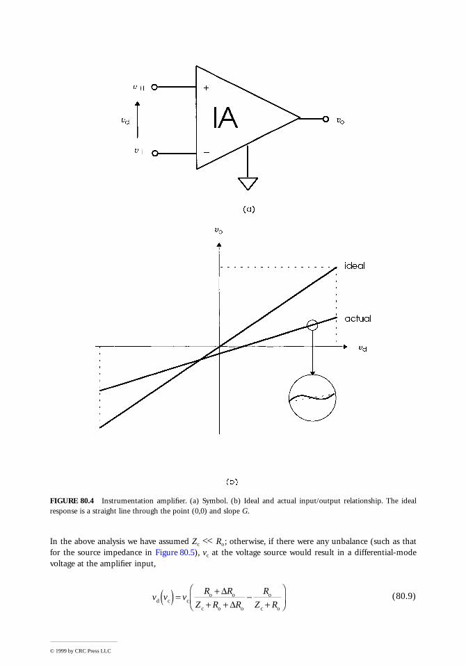
In the above analysis we have assumed Zc << Ro; otherwise, if there were any unbalance (such as thatfor the source impedance in Figure 80.5), vc at the voltage source would result in a differential-modevoltage at the amplifier input,
(80.9)
FIGURE 80.4 Instrumentation amplifier. (a) Symbol. (b) Ideal and actual input/output relationship. The idealresponse is a straight line through the point (0,0) and slope G.
v v vR R
Z R R
R
Z Rd c co o
c o o
o
c o
( ) = ++ +
-+
æ
èçö
ø÷D
D
© 1999 by CRC Press LLC
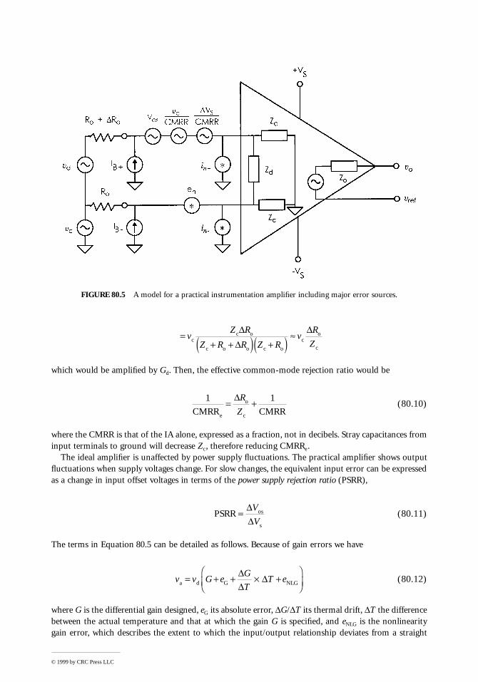
which would be amplified by Gd. Then, the effective common-mode rejection ratio would be
(80.10)
where the CMRR is that of the IA alone, expressed as a fraction, not in decibels. Stray capacitances frominput terminals to ground will decrease Zc, therefore reducing CMRRe.
The ideal amplifier is unaffected by power supply fluctuations. The practical amplifier shows outputfluctuations when supply voltages change. For slow changes, the equivalent input error can be expressedas a change in input offset voltages in terms of the power supply rejection ratio (PSRR),
(80.11)
The terms in Equation 80.5 can be detailed as follows. Because of gain errors we have
(80.12)
where G is the differential gain designed, eG its absolute error, DG/DT its thermal drift, DT the differencebetween the actual temperature and that at which the gain G is specified, and eNLG is the nonlinearitygain error, which describes the extent to which the input/output relationship deviates from a straight
FIGURE 80.5 A model for a practical instrumentation amplifier including major error sources.
vZ R
Z R R Z Rv
R
Zcc o
c o o c o
co
c
=+ +( ) +( ) »D
DD
1 1
CMRR CMRRe
o
c
= +DR
Z
PSRR os
s
= DDV
V
v v G eG
TT ea d G NLG= + + ´ +
æ
èçö
ø÷DD
D
© 1999 by CRC Press LLC

line (insert in Figure 80.4b). The actual temperature TJ is calculated by adding to the current ambienttemperature TA the temperature rise produced by the power PD dissipated in the device. This rise dependson the thermal resistance qJA for the case
(80.13)
where PD can be calculated from the respective voltage and current supplies
(80.14)
The terms for the equivalent input offset error will be
(80.15)
(80.16)
where Ta is the ambient temperature in data sheets, Ios = IB+ – IB– is the offset current, IB = (IB+ + IB–)/2,and all input currents must be calculated at the actual temperature,
(80.17)
Error contributions from finite interference rejection are
(80.18)
where the CMRRe must be that at the frequency for vc, and the PSRR must be that for the frequency ofthe ripple DVs . It is assumed that both frequencies fall inside the bandpass for the signal of interest vd.
The equivalent input voltage noise is
(80.19)
where en2 is the voltage noise power spectral density of the IA, in+
2 and in–2 are the current noise power
spectral densities for each input of the IA, and Be, Bi+, and Bi– are the respective noise equivalentbandwidths of each noise source. In Figure 80.5, the transfer function for each noise source is the sameas that of the signal vd. If the signal bandwidth is determined as fh – f1 by sharp filters, then
(80.20)
(80.21)
where fce and fci are, respectively, the frequencies where the value of voltage and current noise spectraldensities is twice their value at high frequency, also known as corner or 3 dB frequencies.
T T PJ A D JA= + ´ q
P V I V ID S+ S+ S S= + - -
v V TV
TT Tos os a
osJ a= ( ) + ´ -( )D
D
v I I R I R I R I Rb B+ B o B+ o os o B o= -( ) + = +- D D
I I TI
TT T= ( ) + ´ -( )a J a
DD
vv V
rc
e
s
CMRR PSRR= + D
v e B i R B i R Bn n2
e n2
o2
i+ n2
o2
i–= + - + -
B f f ff
fe h 1 ceh
1
= - + ln
B B f f ff
fi+ i– h 1 cih
1
= = - + ln
© 1999 by CRC Press LLC

Another noise specification method states the peak-to-peak noise at a given low-frequency band (fA tofB), usually 0.1 to 10 Hz, and the noise spectral density at a frequency at which it is already constant,normally 1 or 10 kHz. In these cases, if the contribution from noise currents is negligible, the equivalentinput voltage noise can be calculated from
(80.22)
where vnL and vnH are, respectively, the voltage noise in the low-frequency and high-frequency bandsexpressed in the same units (peak-to-peak or rms voltages). To convert rms voltages into peak-to-peakvalues, multiply by 6.6. If the signal bandwidth is from f1 to fh, and f1 = fA and fh > fB, then Equation 80.22can be written
(80.23)
where vnL is the peak-to-peak value and en is the rms voltage noise as specified in data books.Equation 80.23 results in a peak-to-peak calculated noise that is lower than the real noise, because noisespectral density is not constant from fB up. However, it is a simple approach providing useful results.
For signal sources with high output resistors, thermal and excess noise from resistors (see Chapter 54)must be included. For first- and second-order filters, noise bandwidth is slightly larger than signalbandwidth. Motchenbacher and Connelly [4] show how to calculate noise bandwidth, resistor noise, andnoise transfer functions when different from signal transfer functions.
Low-noise design always seeks the minimal bandwidth required for the signal. When amplifying low-frequency signals, if a large capacitor Ci is connected across the input terminals in Figure 80.5, then noiseand interference having a frequency larger than f0 = 1/2p(2Ro)Ci (f0 << fs) will be attenuated.
Another possible source of error for any IA, not included in Equation 80.5, is the slew rate limit of itsoutput stage. Because of the limited current available, the voltage at the output terminal cannot changefaster than a specified value SR. Then, if the maximal amplitude A of an output sine wave of frequency fexceeds
(80.24)
there will be a waveform distortion.Table 80.1 lists some basic specifications for IC instrumentation amplifies whose gain G can be set by
an external resistor or a single connection.
Instrumentation Amplifiers Built from Discrete Parts
Instrumentation amplifiers can be built from discrete parts by using operational amplifiers (op amps)and a few resistors. An op amp is basically a differential voltage amplifier whose gain Ad is very large(from 105 to 107) at dc and rolls off (20 dB/decade) from frequencies of about 1 to 100 Hz, becoming 1at frequencies from 1 to 10 MHz for common models (Figure 80.6a), and whose input impedances areso high (up to 1012 W * * 1 pF) that input currents are almost negligible. Op amps can also be modeledby the circuit in Figure 80.5, and their symbol is that in Figure 80.4a, deleting IA. However, because oftheir large gain, op amps cannot be used directly as amplifiers; a mere 1 mV dc input voltage wouldsaturate any op amp output. Furthermore, op amp gain changes from unit to unit, even for the samemodel, and for a given unit it changes with time, temperature, and supply voltages. Nevertheless, byproviding external feedback, op amps are very flexible and far cheaper than IAs. But when the cost forexternal components and their connections, and overall reliability are also considered, the optimalsolution depends on the situation.
v v vn nL2
nH2= +
v v e f fn nL2
n h B= + ( ) -( )6 62
.
Af
=p
SR
2
© 1999 by CRC Press LLC
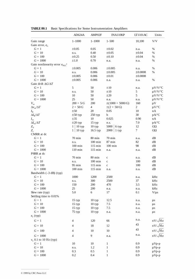
TABLE 80.1 Basic Specifications for Some Instrumentation Amplifiers
AD624A AMP02F INA110KP LT1101AC Units
Gain range 1–1000 1–1000 1–500 10,100 V/VGain error, eG
G = 1 ±0.05 0.05 ±0.02 n.a. %G = 10 n.s. 0.40 ±0.05 ±0.04 %G = 100 ±0.25 0.50 ±0.10 ±0.04 %G = 1000 ±1.0 0.70 n.a. n.a. %
Gain nonlinearity error eNLGa
G = 1 ±0.005 0.006 ±0.005 n.a. %G = 10 n.s. 0.006 ±0.005 ±0.0008 %G = 100 ±0.005 0.006 ±0.01 ±0.0008G = 1000 ±0.005 0.006 n.a. n.a. %
Gain drift DG/DTG = 1 5 50 ±10 n.a. mV/V/°CG = 10 n.s. 50 ±10 5 mV/V/°CG = 100 10 50 ±20 5 mV/V/°CG = 1000 25 50 n.a. n.a. mV/V/°C
Vos 200 + 5/G 200 ±(1000 + 5000/G) 160 mVDvos/DT 2 + 50/G 4 ±(2 + 50/G) 2 mV/°CIB ±50 20 0.05 10 nADIB/DT ±50 typ 250 typ b 30 pA/°CIos ±35 10 0.025 0.90 nADIos/DT ±20 typ 15 typ n.s. 7.0 pA/°CZd 1 ** 10 typ 10 typ 5000 ** 6 typ 12 GWZc 1 ** 10 typ 16.5 typ 2000 ** 1 typ 7 GWCMRR at dc
G = 1 70 min 80 min 70 min n.a. dBG = 10 n.s. 100 min 87 min 82 dBG = 100 100 min 115 min 100 min 98 dBG = 1000 110 min 115 min n.a. n.a. dB
PSRR at dcG = 1 70 min 80 min c n.a. dBG = 10 n.s. 100 min c 100 dBG = 100 95 min 115 min c 100 dBG = 1000 100 min 115 min n.a. n.a. dB
Bandwidth (–3 dB) (typ)G = 1 1000 1200 2500 n.a. kHzG = 10 n.s. 300 2500 37 kHzG = 100 150 200 470 3.5 kHzG = 1000 25 200 n.a. n.a. kHz
Slew rate (typ) 5.0 6 17 0.1 V/msSettling time to 0.01%
G = 1 15 typ 10 typ 12.5 n.a. msG = 10 15 typ 10 typ 7.5 n.a. msG = 100 15 typ 10 typ 7.5 n.a. msG = 1000 75 typ 10 typ n.a. n.a. ms
en (typ)
G = 1 4 120 66 n.a. nV/
G = 10 4 18 12 43 nV/
G = 100 4 10 10 43 nV/
G = 1000 4 9 n.a. n.a. nV/vn 0.1 to 10 Hz (typ)
G = 1 10 10 1 0.9 mVp-pG = 10 n.s. 1.2 1 0.9 mVp-pG = 100 0.3 0.5 1 0.9 mVp-pG = 1000 0.2 0.4 1 0.9 mVp-p
Hz
Hz
Hz
Hz
© 1999 by CRC Press LLC

Figure 80.6b shows an amplifier built from an op amp with external feedback. If input currents areneglected, the current through R2 will flow through R1 and we have
(80.25)
(80.26)
Therefore,
(80.27)
where Gi = 1 + R2/R1 is the ideal gain for the amplifier. If Gi/Ad is small enough (Gi small, Ad large), thegain does not depend on Ad but only on external components. At high frequencies, however, Ad becomessmaller and, from Equation 80.27, vo < Givs so that the bandwidth for the amplifier will reduce for largegains. Franco [5] analyzes different op amp circuits useful for signal conditioning.
Figure 80.7 shows an IA built from three op amps. The input stage is fully differential and the outputstage is a difference amplifier converting a differential voltage into a single-ended output voltage. Differenceamplifiers (op amp and matched resistors) are available in IC form: AMP 03 (Analog Devices) and INA105/6 and INA 117 (Burr-Brown). The gain equation for the complete IA is
(80.28)
Pallás-Areny and Webster [6] have analyzed matching conditions in order to achieve a high CMRR.Resistors R2 do not need to be matched. Resistors R3 and R4 need to be closely matched. A potentiometerconnected to the vref terminal makes it possible to trim the CMRR at low frequencies.
The three-op-amp IA has a symmetrical structure making it easy to design and test. IAs based on anIC difference amplifier do not need any user trim for high CMRR. The circuit in Figure 80.8 is an IAthat lacks these advantages but uses only two op amps. Its gain equation is
in 0.1 to 10 Hz (typ) 60 n.s. n.s. 2.3 pAp-p
in (typ) n.s. 400 1.8 20 fA/
Note: All parameter values are maximum, unless otherwise stated (typ = typical; min = minimum; n.a. =not applicable; n.s. = not specified). Measurement conditions are similar; consult manufacturers’ data booksfor further detail.
a For the INA110, the gain nonlinearity error is specified as percentage of the full-scale output.b Input current drift for the INA110KP approximately doubles for every 10°C increase, from 25°C (10 pA-
typ) to 125°C (10 nA-typ).c The PSRR for the INA110 is specified as an input offset ±(10 + 180/G) mV/V maximum.
TABLE 80.1 (continued) Basic Specifications for Some Instrumentation Amplifiers
AD624A AMP02F INA110KP LT1101AC Units
Hz
v v vR
R Rd s o1= -
+1 2
v A vo d d=
v
v
AR
R
AR
R
G
G
A
o
s
d
d
i
i
d
=+
æ
èçö
ø÷
+ +=
+
1
1 1
2
1
2
1
GR
R
R
R= +
æ
èçö
ø÷1 2 2
1
4
3
© 1999 by CRC Press LLC

FIGURE 80.6 (a) Open loop gain for an op amp. (b) Amplifier based on an op amp with external feedback.
© 1999 by CRC Press LLC
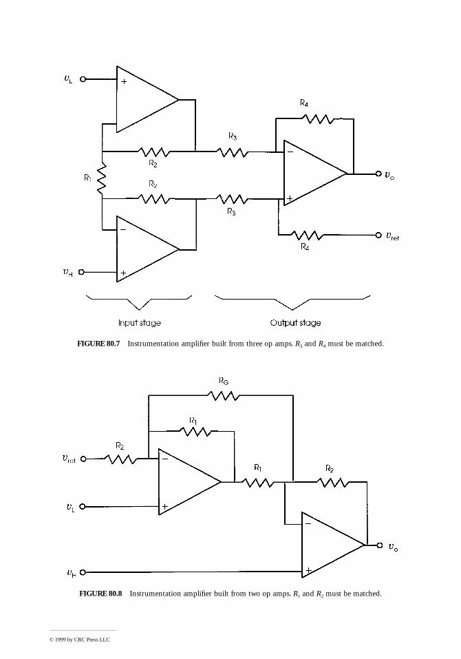
FIGURE 80.7 Instrumentation amplifier built from three op amps. R3 and R4 must be matched.
FIGURE 80.8 Instrumentation amplifier built from two op amps. R1 and R2 must be matched.
© 1999 by CRC Press LLC

(80.29)
R1 and R2 must be matched and RG should be comparable to R2.Another approach to build an IA is by the switched-capacitor technique (Figure 80.9). Switches SW1
and SW2 close together and charge CS (1 mF) to the voltage difference vH – vL; next, SW1 and SW2 openand SW3 and SW4 close, so that CH (0.1 to 1 mF) also charges to vH – vL. Then SW1 and SW2 close again,SW3 and SW4 open, and so on. While CS is being charged CH holds the previous voltage difference.Therefore, the maximal frequency for the input signal must be at least ten times lower than the switchingfrequency. This circuit has a high CMRR because the charge at CS is almost insensitive to the inputcommon-mode voltage. Furthermore, it converts the differential signal to a single-ended voltage. TheLTC 1043 (Linear Technology) includes two sets of four switches to implement this circuit.
Composite Instrumentation Amplifiers
Instrumentation amplifiers have a very limited bandwidth. They achieve a gain of 10 at 2.5 MHz, at best.Moreover, their inputs must be either dc-coupled or, if ac-coupled with input series capacitors, theremust be a path for bias currents; if that path is a resistor from each input to ground, then the common-mode input impedance Zc decreases and noise may increase.
A larger bandwidth for a given gain can be obtained by cascade connection of two or more amplifiers.However, if the additional gain is provided by a single-ended amplifier after the IA, then the overallCMRR is that of the IA, which is small at high frequencies. The circuit in Figure 80.10a is a broadbandIA with large CMRR because the CMRR for the second stage is multiplied by the differential gain forthe first stage, which can be very high if implemented by broadband op amps. The overall gain is
(80.30)
An IA can be ac-coupled by feeding back its dc output to the reference terminal as shown in Figure 80.10b.The high-pass corner frequency is f0 = 1/(2pR0C0).
80.6 Single-Ended Signal Conditioners
Floating signals (single ended or differential) can be connected to amplifiers with single-ended groundedinput. Grounded single-ended can be connected to single-ended amplifiers, provided the difference in
FIGURE 80.9 Instrumentation amplifier based on the switched-capacitor technique. First switches SW1 and SW2close while SW3 and SW4 are open, and CS charges to vH – vL. Then SW1 and SW2 open and SW3 and SW4 close,charging CH to vH – vL.
GR
R
R
R= + +1
22
1
2
G
G G GR
RG= = +
æ
èç
ö
ø÷1 2
2
1 b
a
IA
© 1999 by CRC Press LLC
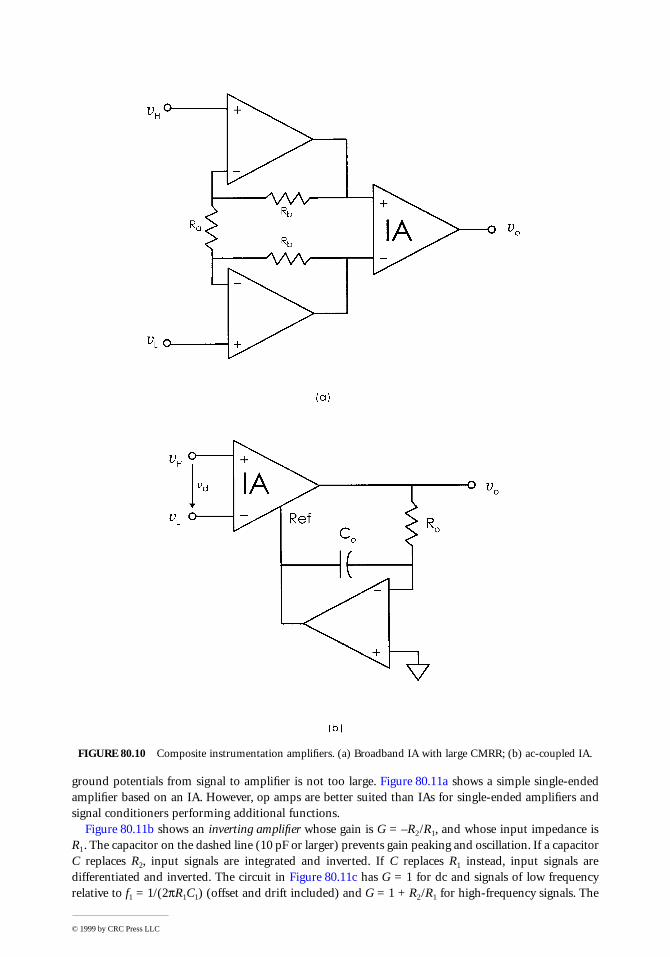
ground potentials from signal to amplifier is not too large. Figure 80.11a shows a simple single-endedamplifier based on an IA. However, op amps are better suited than IAs for single-ended amplifiers andsignal conditioners performing additional functions.
Figure 80.11b shows an inverting amplifier whose gain is G = –R2/R1, and whose input impedance isR1. The capacitor on the dashed line (10 pF or larger) prevents gain peaking and oscillation. If a capacitorC replaces R2, input signals are integrated and inverted. If C replaces R1 instead, input signals aredifferentiated and inverted. The circuit in Figure 80.11c has G = 1 for dc and signals of low frequencyrelative to f1 = 1/(2pR1C1) (offset and drift included) and G = 1 + R2/R1 for high-frequency signals. The
FIGURE 80.10 Composite instrumentation amplifiers. (a) Broadband IA with large CMRR; (b) ac-coupled IA.
© 1999 by CRC Press LLC
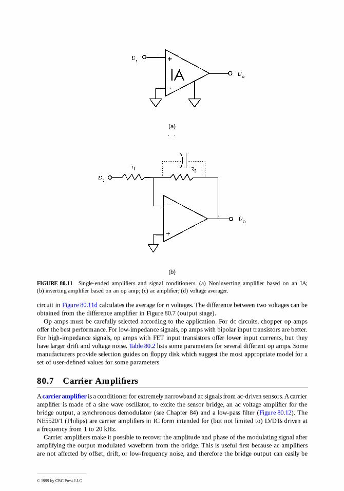
circuit in Figure 80.11d calculates the average for n voltages. The difference between two voltages can beobtained from the difference amplifier in Figure 80.7 (output stage).
Op amps must be carefully selected according to the application. For dc circuits, chopper op ampsoffer the best performance. For low-impedance signals, op amps with bipolar input transistors are better.For high-impedance signals, op amps with FET input transistors offer lower input currents, but theyhave larger drift and voltage noise. Table 80.2 lists some parameters for several different op amps. Somemanufacturers provide selection guides on floppy disk which suggest the most appropriate model for aset of user-defined values for some parameters.
80.7 Carrier Amplifiers
A carrier amplifier is a conditioner for extremely narrowband ac signals from ac-driven sensors. A carrieramplifier is made of a sine wave oscillator, to excite the sensor bridge, an ac voltage amplifier for thebridge output, a synchronous demodulator (see Chapter 84) and a low-pass filter (Figure 80.12). TheNE5520/1 (Philips) are carrier amplifiers in IC form intended for (but not limited to) LVDTs driven ata frequency from 1 to 20 kHz.
Carrier amplifiers make it possible to recover the amplitude and phase of the modulating signal afteramplifying the output modulated waveform from the bridge. This is useful first because ac amplifiersare not affected by offset, drift, or low-frequency noise, and therefore the bridge output can easily be
(a)
(b)
FIGURE 80.11 Single-ended amplifiers and signal conditioners. (a) Noninverting amplifier based on an IA;(b) inverting amplifier based on an op amp; (c) ac amplifier; (d) voltage averager.
© 1999 by CRC Press LLC

amplified. Second, the phase-sensitive demodulator yields not only the amplitude but also the sign of themeasurand. If the measurement range includes positive and negative values for the measurand, phasedetection is essential.
A further advantage of carrier amplifiers is their extremely narrow frequency response, determined bythe output low-pass filter. In the demodulator, the product of the modulated carrier of frequency fc bythe reference signal, also of frequency fc, results in a baseband component and components at nfc (n ³ 2).The output low-pass filter rejects components other than the baseband. If the corner frequency for thisfilter is f0, then the passband for the system is fc ± fo. Therefore, any interference of frequency fi addedto the modulated signal will be rejected if falling outside that passband. The ability to discriminate signalsof interest from those added to them is described by the series (or normal) mode rejection ratio (SMRR),and is usually expressed in decibels. In the present case, using a first-order low-pass filter we have
(80.31)
FIGURE 80.11 (continued)
SMRRo c
o i
c i
0
c i
0
=( )( ) =
+ -( )»
-20 20
120
12
log log logv f
v f
f f
f
f f
f
© 1999 by CRC Press LLC

A power-line interference superimposed on a 10 kHz carrier will undergo an 80-dB attenuation if theoutput low-pass filter has f0 = 1 Hz. The same interference superimposed on the baseband signal wouldbe attenuated by only 35 dB.
TABLE 80.2 Basic Specifications for Operational Amplifiers of Different Technologies
Vos, mV(Dvos/DT)av,
mV/°C IB, pADIB/DT,pA/°C Ios, pA
BWtyp(G = 1),MHz
en(1 kHz),nV/
fce,Hz
vn(p-p), mV
in(1 kHz), fA/
Bipolar
mA741 6000 15 500000 500 200000 1.5 20 200 — 550LM358A 3000 20 100000 — ±30000 1 — — — — LT1028 80 0.8 180000 — 100000 75 0.9 3.5 0.035 1000OP07 75 1.3 3000 50 2800 0.6 9.6 10 0.35 170OP27C 100 1.8 80000 — 75000 8 3.2 2.7 0.09 400OP77A 25 0.3 2000 25 1500 0.6 9.6 10 0.35 170OP177A 10 0.1 1500 25 1000 0.6 — — 0.8 — TLE2021C 600 2 70000 80 3000 1.2 30 — 0.47 90TLE2027C 100 1 90000 — 90000 13 2.5 — 0.05 400
FET input
AD549K 250 5 0.1 b 0.03 typ 1 35 — 4 0.16LF356A 2000 5 50 b 10 4.5 12 — — 10OPA111B 250 1 1 b 0.75 2 7 200 1.2 0.4OPA128J 1000 20 0.3 b 65 1 27 — 4 0.22TL071C 10000 18 200 b 100 3 18 300 4 10TLE2061C 3000 6 4 typ b 2 tip 2 60 20 1.2 1
CMOS
ICL7611A 2 10 typ 50 b 30 0.044 100 800 — 10LMC660C 6000 1.3 typ 20 b 20 1.4 22 — — 0.2LMC6001A 350 10 0.025 b 0.005 1.3 22 — — 0.13TLC271CP 10000 2 typ 0.7 typ c 0.1 typ 2.2 25 100 — n.s.TLC2201C 500 0.1 typ 1 typ d 0.5 typ 1.8 8 — 0.7 0.6
BiMOS
CA3140 15000 8 50 b 30 4.5 40 — — —
CMOS chopper
LTC1052 5 0.05 30 e 30 1.2 — — 1.5 0.6LTC1150C 5 0.05 100 f 200 2.5 — — 1.8 1.8MAX430C 10 0.05 100 g 200 0.5 — — 1.1 10TLC2652AC 1 0.03 4 typ d 2 typ 1.9 23 — 2.8 4TLC2654C 20 0.3 50 typ 0.65 30 typ 1.9 13 — 1.5 4TSC911A 15 0.15 70 — 20 1.5 — — 11 —
Specified values are maximal unless otherwise stated and those for noise, which are typical (typ = typical, av = average;nonspecified parameters are indicated by a dash).
a Values estimated from graphs.b IB doubles every 10°C.c IB doubles every 7.25°C.d IB is almost constant up to 85°C.e IB is almost constant up to 75°C.f IB+ and IB– show a different behavior with temperature.g IB doubles every 10°C above about 65°C.
Hz Hz
© 1999 by CRC Press LLC
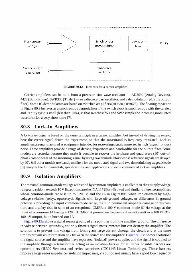
Carrier amplifiers can be built from a precision sine wave oscillator — AD2S99 (Analog Devices),4423 (Burr-Brown), SWR300 (Thaler) — or a discrete-part oscillator, and a demodulator (plus the outputfilter). Some IC demodulators are based on switched amplifiers (AD630, OPA676). The floating capacitorin Figure 80.9 behaves as a synchronous demodulator if the switch clock is synchronous with the carrier,and its duty cycle is small (less than 10%), so that switches SW1 and SW2 sample the incoming modulatedwaveform for a very short time [7].
80.8 Lock-In Amplifiers
A lock-in amplifier is based on the same principle as a carrier amplifier, but instead of driving the sensor,here the carrier signal drives the experiment, so that the measurand is frequency translated. Lock-inamplifiers are manufactured as equipment intended for recovering signals immersed in high (asynchronous)noise. These amplifiers provide a range of driving frequencies and bandwidths for the output filter. Somemodels are vectorial because they make it possible to recover the in-phase and quadrature (90° out-of-phase) components of the incoming signal, by using two demodulators whose reference signals are delayedby 90°. Still other models use bandpass filters for the modulated signal and two demodulating stages. Meade[8] analyzes the fundamentals, specifications, and applications of some commercial lock-in amplifiers.
80.9 Isolation Amplifiers
The maximal common-mode voltage withstood by common amplifiers is smaller than their supply voltagerange and seldom exceeds 10 V. Exceptions are the INA 117 (Burr-Brown) and similar difference amplifierswhose common-mode range is up to ±200 V, and the IA in Figure 80.9 when implemented by high-voltage switches (relays, optorelays). Signals with large off-ground voltages, or differences in groundpotentials exceeding the input common-mode range, result in permanent amplifier damage or destruc-tion, and a safety risk, in spite of an exceptional CMRR: a 100 V common-mode 60 Hz voltage at theinput of a common IA having a 120 dB CMRR at power-line frequency does not result in a 100 V/106 =100 mV output, but a burned-out IA.
Figure 80.13a shows a signal source grounded at a point far from the amplifier ground. The differencein voltage between grounds vi not only thwarts signal measurements but can destroy the amplifier. Thesolution is to prevent this voltage from forcing any large current through the circuit and at the sametime to provide an information link between the source and the amplifier. Figure 80.13b shows a solution:the signal source and the amplifier have separated (isolated) power supplies and the signal is coupled tothe amplifier through a transformer acting as an isolation barrier for vi. Other possible barriers areoptocouplers (IL300-Siemens) and series capacitors (LTC1145-Linear Technology). Those barriersimpose a large series impedance (isolation impedance, Zi) but do not usually have a good low-frequency
FIGURE 80.12 Elements for a carrier amplifier.
© 1999 by CRC Press LLC

response, hence the need to modulate and then demodulate the signal to transfer through it. Thesubsystem made of the modulator and demodulator, plus sometimes an input and an output amplifierand a dc–dc converter for the separate power supply, is called an isolation amplifier. The ability to rejectthe voltage difference across the barrier (isolation-mode voltage, vi) is described by the isolation moderejection ratio (IMRR), expressed in decibels,
(80.32)
Ground isolation also protects people and equipment from contact with high voltage because Zi limitsthe maximal current. Some commercial isolation amplifiers are the AD202, AD204, and AD210 (AnalogDevices) and the ISOxxx series (Burr-Brown).
FIGURE 80.13 (a) A large difference in ground potentials damages amplifiers. (b) An isolation amplifier preventslarge currents caused by this difference from flowing through the circuit.
IMRROUTPUT Voltage
ISOLATION -MODE Voltage= 20 log
© 1999 by CRC Press LLC

Table 80.3 summarizes the compatibility between signal sources and amplifiers. When grounded,amplifiers and signals are assumed to be grounded at different physical points.
80.10 Nonlinear Signal-Processing Techniques
Limiting and Clipping
Clippers or amplitude limiters are circuits whose output voltage has an excursion range restricted to valueslower than saturation voltages. Limiting is a useful signal processing technique for signals having theinformation encoded in parameters other than the amplitude. For example, amplitude limiting is con-venient before homodyne phase demodulators. Limiting can also match output signals levels to thoserequired for TTL circuits (0 to 5 V). Limiting avoids amplifier saturation for large input signal excursions,which would result in a long recovery time before returning to linear operation.
Limiting can be achieved by op amps with diodes and zeners in a feedback loop. Figure 80.14a showsa positive voltage clipper. When vs is positive, vo is negative and R2/R1 times larger; the diode is reversebiased and the additional feedback loop does not affect the amplifier operation. When vs is negative andlarge enough, vo forward biases the diode (voltage drop Vf ) and the zener clamps at Vz , the outputamplitude thus being limited to vo = Vf + Vz until *vs* < (Vf + Vz)R1/R2 (Figure 80.14b). The circuit thenacts again as an inverting amplifier until vs reaches a large negative value.
A negative voltage clipper can be designed by reversing the polarity of the diode and zener. To limitthe voltage in both directions, the diode may be substituted by another zener diode. The output is thenlimited to *vo* < Vz1 + Vf2 for negative inputs to *vo* < Vf1 + Vz2 for positive inputs. If Vz1 = Vz2, then thevoltage limits are symmetrical. Jung [9] gives component values for several precision limiters.
Logarithmic AmplificationThe dynamic range for common linear amplifiers is from 60 to 80 dB. Sensors such as photodetectors,ionizing radiation detectors, and ultrasound receivers can provide signals with an amplitude range widerthan 120 dB. The only way to encompass this wide amplitude range within a narrower range is byamplitude compression. A logarithmic law compresses signals by offering equal-output amplitudechanges in response to a given ratio of input amplitude increase. For example, a scaling of 1 V/decademeans that the output would change by 1 V when the input changes from 10 to 100 mV, or from 100 mVto 1 V. Therefore, logarithmic amplifiers do not necessarily amplify (enlarge) input signals. They are ratherconverters providing a voltage or current proportional to the ratio of the input voltage, or current, to areference voltage, or current.
Logarithmic conversion can be obtained by connecting a bipolar transistor as a feedback element ofan op amp, Figure 80.15a. The collector current iC and the base-emitter voltage have an exponentialrelationship. From the Ebers–Moll model for a transistor, if vCB = 0, then
(80.33)
where vT = kT/q = 25 mV at room temperature, and IS is the saturation current for the transistor. InFigure 80.15a the input voltage is converted into an input current and the op amp forces the collectorcurrent of the transistor to equal the input current, while maintaining vCB » 0 V. Hence, provided iC >>IS, for vs > 0,
(80.34)
The basic circuit in Figure 80.15a must be modified in order to provide temperature stability, phasecompensation, and scale factor correction; reduce bulk resistance error; protect the base-emitter junction;
i I ev vC S
BE T= -( )1
vv
e
v
RIoT s
S
=log
log
© 1999 by CRC Press LLC
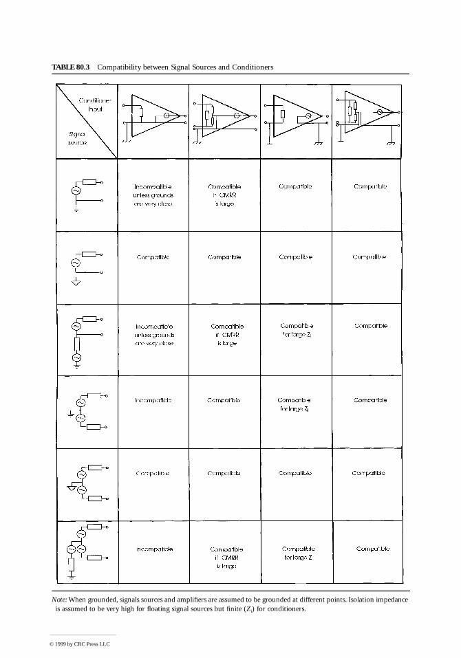
TABLE 80.3 Compatibility between Signal Sources and Conditioners
Note: When grounded, signals sources and amplifiers are assumed to be grounded at different points. Isolation impedance is assumed to be very high for floating signal sources but finite (Zi) for conditioners.
© 1999 by CRC Press LLC
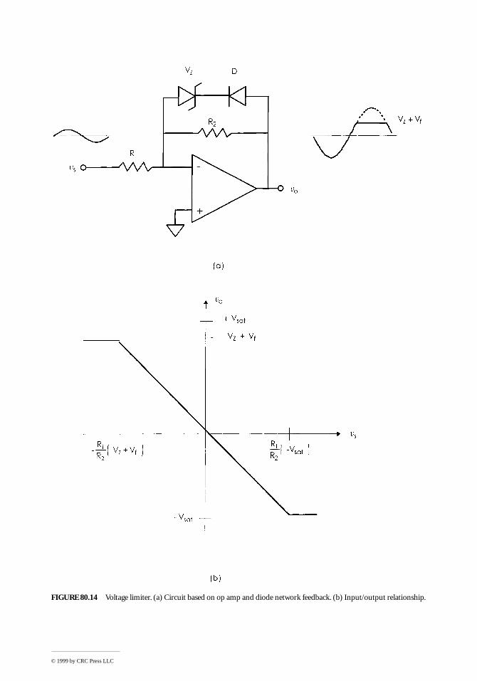
FIGURE 80.14 Voltage limiter. (a) Circuit based on op amp and diode network feedback. (b) Input/output relationship.
© 1999 by CRC Press LLC
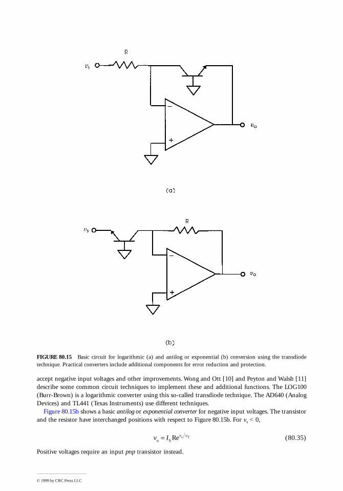
accept negative input voltages and other improvements. Wong and Ott [10] and Peyton and Walsh [11]describe some common circuit techniques to implement these and additional functions. The LOG100(Burr-Brown) is a logarithmic converter using this so-called transdiode technique. The AD640 (AnalogDevices) and TL441 (Texas Instruments) use different techniques.
Figure 80.15b shows a basic antilog or exponential converter for negative input voltages. The transistorand the resistor have interchanged positions with respect to Figure 80.15b. For vs < 0,
(80.35)
Positive voltages require an input pnp transistor instead.
FIGURE 80.15 Basic circuit for logarithmic (a) and antilog or exponential (b) conversion using the transdiodetechnique. Practical converters include additional components for error reduction and protection.
v I v vo S
s T= Re
© 1999 by CRC Press LLC
Multiplication and Division
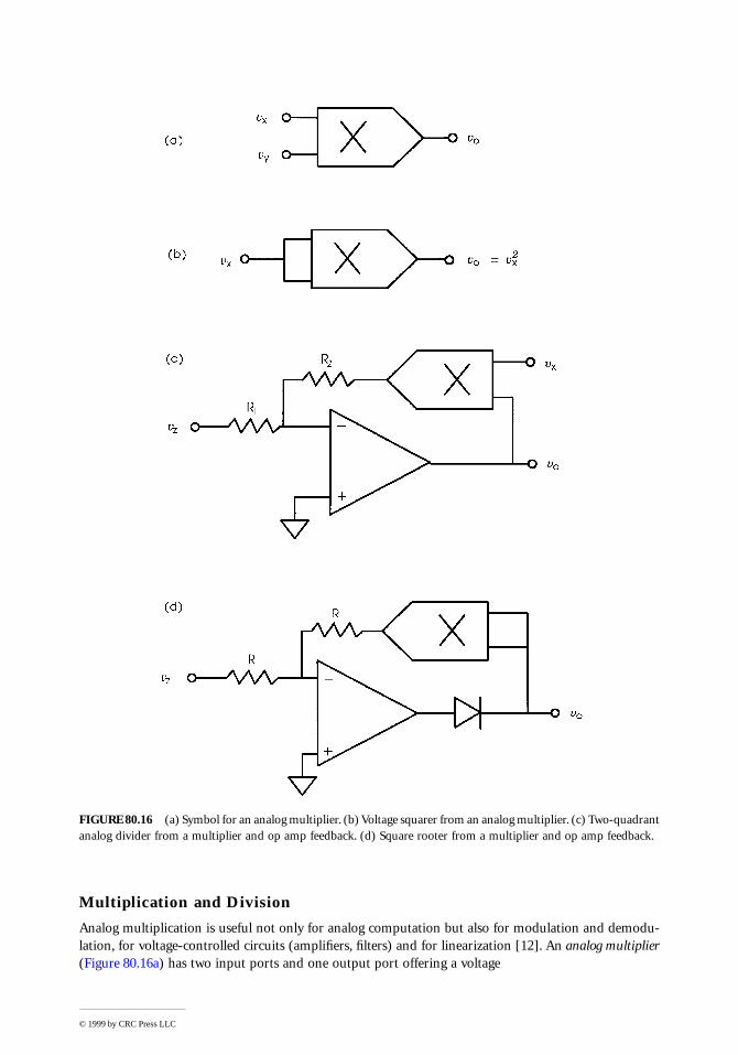
Analog multiplication is useful not only for analog computation but also for modulation and demodu-lation, for voltage-controlled circuits (amplifiers, filters) and for linearization [12]. An analog multiplier(Figure 80.16a) has two input ports and one output port offering a voltage
FIGURE 80.16 (a) Symbol for an analog multiplier. (b) Voltage squarer from an analog multiplier. (c) Two-quadrantanalog divider from a multiplier and op amp feedback. (d) Square rooter from a multiplier and op amp feedback.
© 1999 by CRC Press LLC

(80.36)
where Vm is a constant voltage. If inputs of either polarity are accepted, and their signs preserved, the deviceis a four-quadrant multiplier. If one input is restricted to have a defined polarity but the other can changesign, the device is a two-quadrant multiplier. If both inputs are restricted to only one polarity, the device isan one-quadrant multiplier. By connecting both inputs together, we obtain a voltage squarer (Figure 80.16b).
Wong and Ott10 describe several multiplication techniques. At low frequencies, one-quadrant multi-pliers can be built by the log–antilog technique, based on the mathematical relationships log A + log B =log AB and then antilog (log AB) = AB. The AD538 (Analog Devices) uses this technique. Currently, themost common multipliers use the transconductance method, which provides four-quadrant multiplica-tion and differential ports. The AD534, AD633, AD734, AD834/5 (Analog Devices), and the MPY100and MPY600 (Burr-Brown), are transconductance multipliers. A digital-to-analog converter can be con-sidered a multiplier accepting a digital input and an analog input (the reference voltage). A multipliercan be converted into a divider by using the method in Figure 80.16c. Input vx must be positive in orderfor the op amp feedback to be negative. Then
(80.37)
The log–antilog technique can also be applied to dividing two voltages by first subtracting their logarithmsand then taking the antilog. The DIV100 (Burr-Brown) uses this technique. An analog-to-digital convertercan be considered a divider with digital output and one dc input (the reference voltage). A multipliercan also be converted into a square rooter as shown in Figure 80.16d. The diode is required to preventcircuit latch-up [10]. The input voltage must be negative.
80.11 Analog Linearization
Nonlinearity in instrumentation can result from the measurement principle, from the sensor, or fromsensor conditioning. In pressure-drop flowmeters, for example, the drop in pressure measured is pro-portional to the square of the flow velocity; hence, flow velocity can be obtained by taking the squareroot of the pressure signal. The circuit in Figure 80.16d can perform this calculation. Many sensors arelinear only in a restricted measurand range; other are essentially nonlinear (NTC, LDR); still others arelinear in some ranges but nonlinear in other ranges of interest (thermocouples). Linearization techniquesfor particular sensors are described in the respective chapters.
Nonlinearity attributable to sensor conditioning is common, for example, when resistive (linear)sensors are placed in voltage dividers or bridges. The Wheatstone bridge in Figure 80.17a, for example,includes a linear sensor but yields a nonlinear output voltage,
(80.38)
The nonlinearity arises from the dependence of the current through the sensor on its resistance, becausethe bridge is supplied at a constant voltage. The circuit in Figure 80.17b provides a solution based onone op amp which forces a constant current V/R0 through the sensor. The bridge output voltage is
(80.39)
In addition, vs is single ended. The op amp must have a good dc performance.
vv v
Vox y
m
=
v VR
R
v
vo mz
x
= - 2
1
v Vx
x
Vx
xs = +
+-
æ
èçö
ø÷=
+( )1
2
1
2 2 2
vV v
Vx
sa= + =
2 2
© 1999 by CRC Press LLC
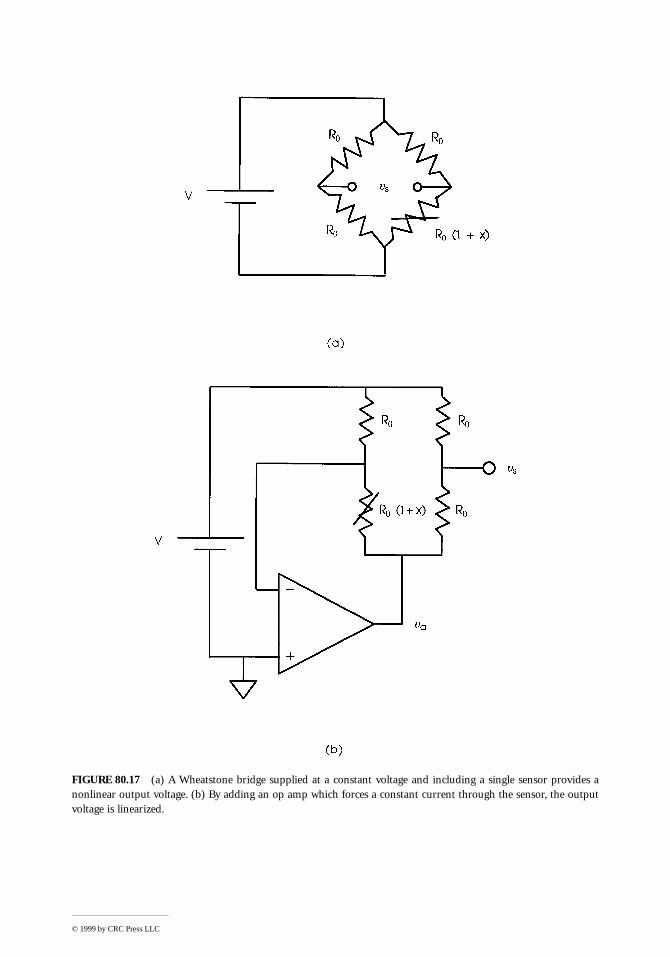
FIGURE 80.17 (a) A Wheatstone bridge supplied at a constant voltage and including a single sensor provides anonlinear output voltage. (b) By adding an op amp which forces a constant current through the sensor, the outputvoltage is linearized.
© 1999 by CRC Press LLC
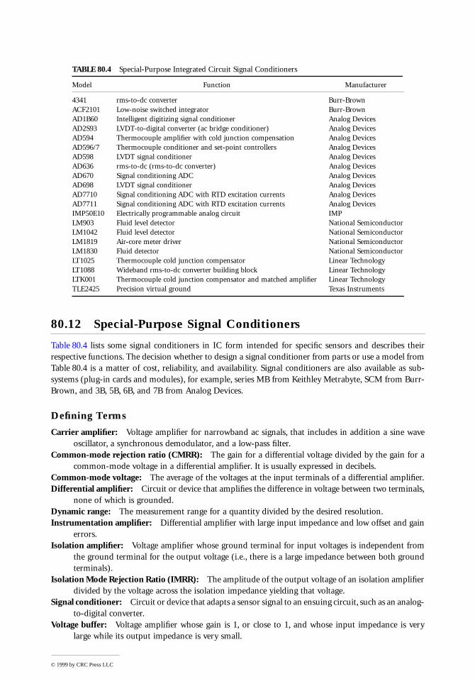
80.12 Special-Purpose Signal Conditioners
Table 80.4 lists some signal conditioners in IC form intended for specific sensors and describes theirrespective functions. The decision whether to design a signal conditioner from parts or use a model fromTable 80.4 is a matter of cost, reliability, and availability. Signal conditioners are also available as sub-systems (plug-in cards and modules), for example, series MB from Keithley Metrabyte, SCM from Burr-Brown, and 3B, 5B, 6B, and 7B from Analog Devices.
Defining Terms
Carrier amplifier: Voltage amplifier for narrowband ac signals, that includes in addition a sine waveoscillator, a synchronous demodulator, and a low-pass filter.
Common-mode rejection ratio (CMRR): The gain for a differential voltage divided by the gain for acommon-mode voltage in a differential amplifier. It is usually expressed in decibels.
Common-mode voltage: The average of the voltages at the input terminals of a differential amplifier.Differential amplifier: Circuit or device that amplifies the difference in voltage between two terminals,
none of which is grounded.Dynamic range: The measurement range for a quantity divided by the desired resolution.Instrumentation amplifier: Differential amplifier with large input impedance and low offset and gain
errors.Isolation amplifier: Voltage amplifier whose ground terminal for input voltages is independent from
the ground terminal for the output voltage (i.e., there is a large impedance between both groundterminals).
Isolation Mode Rejection Ratio (IMRR): The amplitude of the output voltage of an isolation amplifierdivided by the voltage across the isolation impedance yielding that voltage.
Signal conditioner: Circuit or device that adapts a sensor signal to an ensuing circuit, such as an analog-to-digital converter.
Voltage buffer: Voltage amplifier whose gain is 1, or close to 1, and whose input impedance is verylarge while its output impedance is very small.
TABLE 80.4 Special-Purpose Integrated Circuit Signal Conditioners
Model Function Manufacturer
4341 rms-to-dc converter Burr-BrownACF2101 Low-noise switched integrator Burr-BrownAD1B60 Intelligent digitizing signal conditioner Analog DevicesAD2S93 LVDT-to-digital converter (ac bridge conditioner) Analog DevicesAD594 Thermocouple amplifier with cold junction compensation Analog DevicesAD596/7 Thermocouple conditioner and set-point controllers Analog DevicesAD598 LVDT signal conditioner Analog DevicesAD636 rms-to-dc (rms-to-dc converter) Analog DevicesAD670 Signal conditioning ADC Analog DevicesAD698 LVDT signal conditioner Analog DevicesAD7710 Signal conditioning ADC with RTD excitation currents Analog DevicesAD7711 Signal conditioning ADC with RTD excitation currents Analog DevicesIMP50E10 Electrically programmable analog circuit IMPLM903 Fluid level detector National SemiconductorLM1042 Fluid level detector National SemiconductorLM1819 Air-core meter driver National SemiconductorLM1830 Fluid detector National SemiconductorLT1025 Thermocouple cold junction compensator Linear TechnologyLT1088 Wideband rms-to-dc converter building block Linear TechnologyLTK001 Thermocouple cold junction compensator and matched amplifier Linear TechnologyTLE2425 Precision virtual ground Texas Instruments
© 1999 by CRC Press LLC

References
1. R. Pallás-Areny and J.G. Webster, Sensors and Signal Conditioning, New York: John Wiley & Sons, 1991.2. J. Graeme, Photodiode Amplifiers, Op Amp Solutions, New York: McGraw-Hill, 1996.3. C. Kitchin and L. Counts, Instrumentation Amplifier Application Guide, 2nd ed., Application Note,
Norwood, MA: Analog Devices, 1992.4. C.D. Motchenbacher and J.A. Connelly, Low-Noise Electronic System Design, New York: John
Wiley & Sons, 1993.5. S. Franco, Design with Operational Amplifiers and Analog Integrated Circuits, 2nd ed., New York:
McGraw-Hill, 1998.6. R. Pallás-Areny and J.G. Webster, Common mode rejection ratio in differential amplifiers, IEEE
Trans. Instrum. Meas., 40, 669–676, 1991.7. R. Pallás-Areny and O. Casas, A novel differential synchronous demodulator for ac signals, IEEE
Trans. Instrum. Meas., 45, 413–416, 1996.8. M.L. Meade, Lock-in Amplifiers: Principles and Applications, London: Peter Peregrinus, 1984.9. W.G. Jung, IC Op Amp Cookbook, 3rd ed., Indianapolis, IN: Howard W. Sams, 1986.
10. Y.J. Wong and W.E. Ott, Function Circuits Design and Application, New York: McGraw-Hill, 1976.11. A.J. Peyton and V. Walsh, Analog Electronics with Op Amps, Cambridge, U.K.: Cambridge University
Press, 1993.12. D.H. Sheingold, Ed., Multiplier Application Guide, Norwood, MA: Analog Devices, 1978.
Further Information
B.W.G. Newby, Electronic Signal Conditioning, Oxford, U.K.: Butterworth-Heinemann, 1994, is a bookfor those in the first year of an engineering degree. It covers analog and digital techniques at beginners’level, proposes simple exercises, and provides clear explanations supported by a minimum of equations.
P. Horowitz and W. Hill, The Art of Electronics, 2nd ed., Cambridge, U.K.: Cambridge University Press,1989. This is a highly recommended book for anyone interested in building electronic circuits withoutworrying about internal details for active components.
M.N. Horenstein, Microelectronic Circuits and Devices, 2nd ed., Englewood Cliffs, NJ: Prentice-Hall,1996, is an introductory electronics textbook for electrical or computer engineering students. It providesmany examples and proposes many more problems, for some of which solutions are offered.
J. Dostál, Operational Amplifiers, 2nd ed., Oxford, U.K.: Butterworth-Heinemann, 1993, provides agood combination of theory and practical design ideas. It includes complete tables which summarizeserrors and equivalent circuits for many op amp applications.
T.H. Wilmshurst, Signal Recovery from Noise in Electronic Instrumentation, 2nd ed., Bristol, U.K.: AdamHilger, 1990, describes various techniques for reducing noise and interference in instrumentation. Noreferences are provided and some demonstrations are rather short, but it provides insight into veryinteresting topics.
Manufacturers’ data books provide a wealth of information, albeit nonuniformly. Application notesfor special components should be consulted before undertaking any serious project. In addition, appli-cation notes provide handy solutions to difficult problems and often inspire good designs. Most manu-facturers offer such literature free of charge. The following have shown to be particularly useful and easyto obtain: 1993 Applications Reference Manual, Analog Devices; 1994 IC Applications Handbook, Burr-Brown; 1990 Linear Applications Handbook and 1993 Linear Applications Handbook Vol. II, Linear Tech-nology; 1994 Linear Application Handbook, National Semiconductor; Linear and Interface Circuit Appli-cations, Vols. 1, 2, and 3, Texas Instruments.
R. Pallás-Areny and J.G. Webster, Analog Signal Processing, New York: John Wiley & Sons, 1999, offersa design-oriented approach to processing instrumentation signals using standard analog integrated cir-cuits, that relies on signal classification, analog domain conversions, error analysis, interference rejectionand noise reduction, and highlights differential circuits.
© 1999 by CRC Press LLC