Embed Size (px)
Citation preview
PN 1014249 Rev A Logic Product Development Company, All Rights Reserved i
AM35x SOM-M2 Hardware Specification Hardware Documentation
Logic PD // Products Published: November 2009 Last revised: July 2010
This document contains valuable proprietary and confidential information and the attached file contains source code, ideas, and techniques that are owned by Logic Product Development Company (collectively “Logic PD’s Proprietary Information”). Logic PD’s Proprietary Information may not be used by or disclosed to any third party except under written license from Logic Product Development Company.
Logic Product Development Company makes no representation or warranties of any nature or kind regarding Logic PD’s Proprietary Information or any products offered by Logic Product Development Company. Logic PD’s Proprietary Information is disclosed herein pursuant and subject to the terms and conditions of a duly executed license or agreement to purchase or lease equipment. The only warranties made by Logic Product Development Company, if any, with respect to any products described in this document are set forth in such license or agreement. Logic Product Development Company shall have no liability of any kind, express or implied, arising out of the use of the Information in this document, including direct, indirect, special or consequential damages.
Logic Product Development Company may have patents, patent applications, trademarks, copyrights, trade secrets, or other intellectual property rights pertaining to Logic PD’s Proprietary Information and products described in this document (collectively “Logic PD’s Intellectual Property”). Except as expressly provided in any written license or agreement from Logic Product Development Company, this document and the information contained therein does not create any license to Logic PD’s Intellectual Property.
The Information contained herein is subject to change without notice. Revisions may be issued regarding changes and/or additions.
© Copyright 2010, Logic Product Development Company. All Rights Reserved.
AM35x SOM-M2 Hardware Specification
PN 1014249 Rev A Logic Product Development Company, All Rights Reserved ii
Revision History
REV EDITOR REVISION DESCRIPTION Schematic PN & REV APPROVAL DATE
1 CM Initial Release 1013603 Rev B JCA 10/04/09
2 JCA Beta Release 1013603 Rev B JCA 11/04/09
3 CM
-Section 3.2: Updated DC Main Battery Active Current measurement and clarified note explaining the conditions of that measurement; Added note 4 regarding the 802.11 measurements; -Section 6.3: Changed J3.36 to RFU from NAND_nCS; Changed voltages for J3.35 and J3.37 to 1.8V from 3.3V or 1.8V; Changed J3.39 to UART_DBG from RFU; Changed J3.41 to BT_DBG from RFU; Changed J3.46 to NAND_SEL from RFU -Minor grammatical edits throughout
1014320 Rev A NJK 02/18/10
4 JCA
-Added Sections 2.3.4 & 2.3.5 to point to the Appendices for mechanical drawings -Added Example Retention Methods mechanical drawings -Section 3.10.2: Corrected number of McBSPs available on the SOM to four since McBSP5 is used by the uP_HSBUSB signal.
1014320 Rev A JCA 04/02/10
5 JCA
-Section 3.6 & 3.7: Updated MAC address sticker information; -Section 3.7.1: Added note about FM interface; -Section 4.5.1.1: Corrected supported voltage range for MAIN_BATT_IN input; -Section 6.2 pins J2.49–52: Updated voltage and signal descriptions for MAIN_BATT_IN
1014320 Rev A CM 05/27/10
A JCA, NJK
Official Release -Added FCC Certification language throughout; -Added 802.11n protocol throughout; -Changed AM3517 microprocessor core to 600 MHz per TI spec; -Section 2.3.1: Updated height for wireless configuration; Updated weight for standard configuration SOM; -Section 2.3.3: Added antenna note pertaining to FCC guidelines; -Section 2.4: Added Industrial Temp range and note that Industrial Temp models do not include Wi-Fi/BT; -Section 3.1: Added USB0 and USB1 voltage parameters; -Section 3.2: Updated Note 3 to indicate the Main Battery Active Current was measured using a fully-populated SOM and the LCD current was not included in the measurement; Added USB0 and USB1 voltage parameters; Added 802.11n parameters. -Added Section 3.7.1: 2.4GHz Antenna Information; -Added Section 3.7.2: Wireless Software Requirements; -Section 3.11: Updated USB information to reflect what is available on the SOM, not the microprocessor; -Section 4.2: Corrected typo in reset signal names; -Section 6.1: Throughout, updates to clarify signal descriptions; J1.37 added microprocessor name and voltage; J1.85 specified signal as Input and 5V, was N/A; Specified or changed IO direction on J1.70, 89, 91; Added clarification to Note 1 that all IO pins must be set to same voltage; -Section 6.2: Throughout, updates to clarify signal descriptions; J2.57 &J2.63 signal descriptions were reversed for Ethernet activity and speed LEDs, this has been corrected; J2.84 description mistakenly called out McBSP1 instead of McBSP2; Specified or changed IO direction on J2.17, 34, 36, 38, 40, 42, 44, 46, 72, 78, 81, 82, 84-86, 88; Added clarification to Note 1 that all IO pins must be set to same voltage; -Section 6.3: Throughout, updates to clarify signal descriptions; J3.16 changed direction to Input and updated description; J3.26 description mistakenly called out McBSP4 instead of McBSP3; J3.47 changed direction to Output, voltage to 3.3V, and updated description; Specified or changed IO direction on J3.1-5, 7-13, 15, 23-29, 77, 85-88; Added clarification to Note 1 that all IO pins must be set to same voltage; -Added mechanical drawing for AM35x SOM-M2 with wireless
1015592 Rev A NJK 07/22/10
Please check www.logicpd.com for the latest revision of this specification and other documents.

AM35x SOM-M2 Hardware Specification
PN 1014249 Rev A Logic Product Development Company, All Rights Reserved iii
FCC Certification
This device complies with part 15 of the FCC Rules. Operation is subject to the following two conditions: (1) This device may not cause harmful interference, and (2) this device must accept any interference received, including interference that may cause undesired operation. Any changes or modifications not expressly approved by Logic PD could void the user's authority to use this device. See Application Note 447 for FCC guidelines pertaining to use of this device in end products. NOTE: This equipment has been tested and found to comply with the limits for a Class B digital device, pursuant to part 15 of the FCC Rules. These limits are designed t o provide reasonable protection against harmful interference in a residential installation. This equipment generates, uses and can radiate radio frequency energy and, if not installed and used in accordance with the instructions, may cause harmful interference to radio communications. However, there is no guarantee that interference will not occur in a particular installation. If this equipment does cause harmful interference to radio or television reception, which can be determined by turning the equipment off and on, the user is encouraged to try to correct the interference by one or more of the following measures: —Reorient or relocate the receiving antenna. —Increase the separation between the equipment and receiver. —Connect the equipment into an outlet on a circuit different from that to which the receiver is connected. —Consult the dealer or an experienced radio/TV technician for help.
AM35x SOM-M2 Hardware Specification
PN 1014249 Rev A Logic Product Development Company, All Rights Reserved iv
Table of Contents
1 Introduction ........................................................................................................................................... 1 1.1 Product Overview ............................................................................................................................. 1 1.2 Abbreviations, Acronyms, & Definitions ........................................................................................... 1 1.3 Nomenclature ................................................................................................................................... 2 1.4 Scope of Document .......................................................................................................................... 2 1.5 Additional Documentation Resources .............................................................................................. 2
2 Functional Specification ...................................................................................................................... 4 2.1 Microprocessor ................................................................................................................................. 4
2.1.1 AM35x Microprocessor .............................................................................................................. 4 2.1.2 AM35x Microprocessor Block Diagram ..................................................................................... 5
2.2 SOM Interface .................................................................................................................................. 5 2.2.1 AM35x SOM-M2 Block Diagram................................................................................................ 6
2.3 Mechanical Specifications ................................................................................................................ 6 2.3.1 Mechanical Characteristics of SOM-M2 .................................................................................... 6 2.3.2 Interface Connectors ................................................................................................................. 7 2.3.3 Wireless Antenna Connection ................................................................................................... 7 2.3.4 AM35x SOM-M2 Mechanical Drawings ..................................................................................... 7 2.3.5 Example AM35x SOM-M2 Retention Methods .......................................................................... 7
2.4 Temperature Specifications ............................................................................................................. 7 3 Electrical Specification ........................................................................................................................ 8
3.1 Absolute Power Maximum Ratings .................................................................................................. 8 3.2 Recommended Power Operating Conditions................................................................................... 8 3.3 Clocks............................................................................................................................................... 8 3.4 Memory ............................................................................................................................................ 9
3.4.1 Memory Management Unit (MMU) ............................................................................................ 9 3.4.2 DDR ........................................................................................................................................... 9 3.4.3 NAND Flash ............................................................................................................................... 9 3.4.4 MMC/SD Support .................................................................................................................... 10
3.5 DMA ............................................................................................................................................... 10 3.6 10/100 Ethernet PHY ..................................................................................................................... 10 3.7 802.11 Wireless Ethernet + Bluetooth ........................................................................................... 10
3.7.1 2.4 GHz Antenna Information .................................................................................................. 11 3.7.2 Software Requirements ........................................................................................................... 11 3.7.3 FM Interface............................................................................................................................. 11
3.8 Display Interface ............................................................................................................................ 11 3.9 Video Processing Front End .......................................................................................................... 12
3.9.1 TV_OUT ................................................................................................................................... 12 3.10 Serial Interfaces ............................................................................................................................. 12
3.10.1 CAN Controller......................................................................................................................... 12 3.10.2 McBSP ..................................................................................................................................... 13 3.10.3 UARTs ..................................................................................................................................... 13 3.10.4 McSPI ...................................................................................................................................... 13 3.10.5 I2C ........................................................................................................................................... 13
3.10.5.1 I2C1 ................................................................................................................................... 14 3.11 USB Interface ................................................................................................................................. 14 3.12 ADC/Touch Interface ...................................................................................................................... 15 3.13 Real Time Clock (RTC) .................................................................................................................. 15 3.14 General Purpose I/O (GPIO) .......................................................................................................... 15 3.15 Sysboot I/O .................................................................................................................................... 15 3.16 Expansion/Feature Options ........................................................................................................... 15
4 System Integration ............................................................................................................................. 17 4.1 Custom Configuration .................................................................................................................... 17 4.2 Resets ............................................................................................................................................ 17
AM35x SOM-M2 Hardware Specification
PN 1014249 Rev A Logic Product Development Company, All Rights Reserved v
4.2.1 Master Reset (RESPWRONn)—Reset Input .......................................................................... 17 4.2.2 SOM-M2 Reset (RESOUTn)—Reset Output .......................................................................... 17 4.2.3 SOM-M2 Reset (uP_RESWARMn)—Reset Input/Output ....................................................... 18
4.3 Interrupts ........................................................................................................................................ 18 4.4 JTAG Debugger Interface .............................................................................................................. 18 4.5 Power Management ....................................................................................................................... 18
4.5.1 System Power Supplies ........................................................................................................... 18 4.5.1.1 MAIN_BATT_IN ................................................................................................................ 18 4.5.1.2 VRTC_IN ........................................................................................................................... 19
4.5.2 Dual Voltage I/O ...................................................................................................................... 19 4.5.3 System Power Management ................................................................................................... 19 4.5.4 System Power Sequencing ..................................................................................................... 19
4.6 ESD Considerations ....................................................................................................................... 19 5 Memory & I/O Mapping ....................................................................................................................... 21 6 Pin Descriptions & Functions ........................................................................................................... 22
6.1 J1 Connector 100-Pin Descriptions ............................................................................................... 22 6.2 J2 Connector 100-Pin Descriptions ............................................................................................... 26 6.3 J3 Connector 100-Pin Descriptions ............................................................................................... 30
Appendix A: AM35x SOM-M2 Mechanical Drawing (with Wireless)..................................................... 37 Appendix B: AM35x SOM-M2 Mechanical Drawing (without Wireless) ............................................... 39 Appendix C: Example AM35x SOM-M2 Retention Methods ................................................................. 41
AM35x SOM-M2 Hardware Specification
PN 1014249 Rev A Logic Product Development Company, All Rights Reserved vi
Table of Figures Figure 2.1: AM35x Microprocessor Block Diagram ...................................................................................... 5Figure 2.2: AM35x SOM-M2 Block Diagram ................................................................................................. 6Table 2.1: Board-to-Board Socket Connectors Manufacturer Information ................................................... 7Table 2.2: Wireless Antenna Cable Manufacturer Information ..................................................................... 7Table 3.1: AM3517Microprocessor Clocks ................................................................................................... 9Table 3.2: I2C1 Bus Devices & Addresses ................................................................................................. 14Table 3.3: Boot Strap Options ..................................................................................................................... 15Table 5.1: Chip Select Signals .................................................................................................................... 21
AM35x SOM-M2 Hardware Specification
PN 1014249 Rev A Logic Product Development Company, All Rights Reserved 1
1 Introduction
1.1 Product Overview
The AM35x System on Module (SOM) is a compact, product-ready hardware and software solution that fast forwards embedded designs. Based on Texas Instruments’ Sitara AM35x microprocessor and designed in the SOM-M2 form factor, the AM35x SOM-M2 offers essential features for handheld and embedded networking applications.
The SOM-M2 is an off-the-shelf solution that allows customers to focus on their high-value core technologies. The standard SOM-M2 form factor allows developers to reuse existing baseboard designs when upgrading to new AM processors, which extends roadmap possibilities for their end-product. By starting with the corresponding AM3517 EVM or eXperimenter Development Kit, engineers can write application software on the same hardware that will be used in the final product.
The AM35x SOM-M2 is ideal for medical patient monitoring wearables and other portable instrumentation applications. The AM3517 includes an SGX530 graphics accelerator and multiple communication ports, including Bluetooth, wireless 802.11b/g/n, and wired 10/100 Ethernet. For commercial signage, medical imaging, avionics, and industrial displays, the AM3517 SOM-M2 allows for powerful versatility, long-life, and greener products.
1.2 Abbreviations, Acronyms, & Definitions ADC Analog to Digital Converter BSP Board Support Package BTB Board-to-Board DDR Double Data Rate (RAM) DMA Direct Memory Access ESD Electrostatic Discharge FIFO First In First Out GPIO General Purpose Input Output GPMC General Purpose Memory Controller GPO General Purpose Output HECC High End CAN Controller I2C Inter-Integrated Circuit I2S Inter-Integrated Circuit Sound IDC Insulation Displacement Connector IC Integrated Circuit I/O Input/Output IRQ Interrupt Request LCD Liquid Crystal Display LDO Low Dropout (Regulator) McBSP Multi-channel Buffered Serial Port OTG On-the-Go (USB) PCB Printed Circuit Board PCMCIA Personal Computer Memory Card International Association (PC Cards) PHY Physical Layer PLL Phase Lock Loop PWM Pulse Width Modulation RTC Real Time Clock SCC Standard CAN Controller SDIO Secure Digital Input Output
AM35x SOM-M2 Hardware Specification
PN 1014249 Rev A Logic Product Development Company, All Rights Reserved 2
SDRAM Synchronous Dynamic Random Access Memory SCCB Serial Camera Control Bus SOM System on Module SOM-M2 SOM form factor type SSP Synchronous Serial Port SPI Standard Programming Interface STN Super-Twisted Nematic (LCD) TFT Thin Film Transistor (LCD) TI Texas Instruments TLB Translation Look-Aside Buffer TSC Touch Screen Controller TTL Transistor-Transistor Logic UART Universal Asynchronous Receive Transmit
1.3 Nomenclature
■ The terms “SOM” and “SOM-M2” are used interchangeably throughout this document and can be assumed to mean the same thing within this text. The SOM-M2 is a specific form factor type of Logic PD’s SOM.
■ Within this document, AM35x is used to denote the AM3505 and AM3517 microprocessors; where differences between microprocessor features occur, the specific microprocessor name is used.
1.4 Scope of Document
■ This Hardware Specification is unique to the design and use of the AM3517 SOM-M2 as designed by Logic PD and does not intend to include information outside of that scope. Detailed information about the Texas Instruments (TI) AM3517 microprocessor or any other device component on the SOM can be found in their respective manuals and specification documents; please see Section 1.5 for additional resources.
1.5 Additional Documentation Resources
The following documents or documentation resources are referenced within this Hardware Specification.
■ TI’s AM3517/05 ARM Microprocessor Datasheet, Technical Reference Manual, User Guides, Application Notes, White Papers, and Errata http://www.ti.com/am3517
■ TI’s TPS65023 Datasheet http://focus.ti.com/docs/prod/folders/print/tps65023.html
■ TI’s TSC2004 Datasheet http://focus.ti.com/docs/prod/folders/print/tsc2004.html
■ ARM Cortex-A8 Technical Reference Manual http://infocenter.arm.com/help/index.jsp.
■ USB 2.0 Specification, available from USB.org http://www.usb.org/developers/docs/
■ U-Boot documentation http://www.denx.de/wiki/U-Boot/WebHome
■ Logic PD AM3517 SOM-M2 BOM, Schematic, and Layout http://support.logicpd.com/downloads/1238/
AM35x SOM-M2 Hardware Specification
PN 1014249 Rev A Logic Product Development Company, All Rights Reserved 3
■ Logic PD AM3517 eXperimenter Baseboard BOM, Schematic, and Layout http://support.logicpd.com/downloads/1239/
■ Logic PD AM3517 Application Board BOM, Schematic, and Layout http://support.logicpd.com/downloads/1240/
AM35x SOM-M2 Hardware Specification
PN 1014249 Rev A Logic Product Development Company, All Rights Reserved 4
2 Functional Specification
2.1 Microprocessor
2.1.1 AM35x Microprocessor
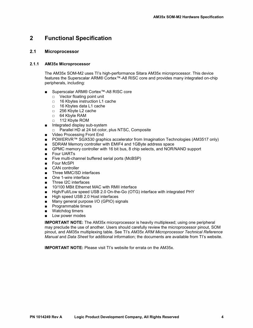
The AM35x SOM-M2 uses TI’s high-performance Sitara AM35x microprocessor. This device features the Superscalar ARM® Cortex™-A8 RISC core and provides many integrated on-chip peripherals, including:
■ Superscalar ARM® Cortex™-A8 RISC core □ Vector floating point unit □ 16 Kbytes instruction L1 cache □ 16 Kbytes data L1 cache □ 256 Kbyte L2 cache □ 64 Kbyte RAM □ 112 Kbyte ROM
■ Integrated display sub-system □ Parallel HD at 24 bit color, plus NTSC, Composite
■ Video Processing Front End ■ POWERVR™ SGX530 graphics accelerator from Imagination Technologies (AM3517 only) ■ SDRAM Memory controller with EMIF4 and 1GByte address space ■ GPMC memory controller with 16 bit bus, 8 chip selects, and NOR/NAND support ■ Four UARTs ■ Five multi-channel buffered serial ports (McBSP) ■ Four McSPI ■ CAN controller ■ Three MMC/SD interfaces ■ One 1-wire interface ■ Three I2C interfaces ■ 10/100 MBit Ethernet MAC with RMII interface ■ High/Full/Low speed USB 2.0 On-the-Go (OTG) interface with integrated PHY ■ High speed USB 2.0 Host interfaces ■ Many general purpose I/O (GPIO) signals ■ Programmable timers ■ Watchdog timers ■ Low power modes IMPORTANT NOTE: The AM35x microprocessor is heavily multiplexed; using one peripheral may preclude the use of another. Users should carefully review the microprocessor pinout, SOM pinout, and AM35x multiplexing table. See TI’s AM35x ARM Microprocessor Technical Reference Manual and Data Sheet for additional information; the documents are available from TI’s website.
IMPORTANT NOTE: Please visit TI’s website for errata on the AM35x.
AM35x SOM-M2 Hardware Specification
PN 1014249 Rev A Logic Product Development Company, All Rights Reserved 5
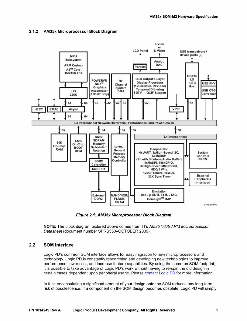
2.1.2 AM35x Microprocessor Block Diagram
Figure 2.1: AM35x Microprocessor Block Diagram
NOTE: The block diagram pictured above comes from TI’s AM3517/05 ARM Microprocessor Datasheet (document number SPRS550–OCTOBER 2009).
2.2 SOM Interface
Logic PD’s common SOM interface allows for easy migration to new microprocessors and technology. Logic PD is constantly researching and developing new technologies to improve performance, lower cost, and increase feature capabilities. By using the common SOM footprint, it is possible to take advantage of Logic PD’s work without having to re-spin the old design in certain cases dependent upon peripheral usage. Please contact Logic PD for more information.
In fact, encapsulating a significant amount of your design onto the SOM reduces any long-term risk of obsolescence. If a component on the SOM design becomes obsolete, Logic PD will simply
AM35x SOM-M2 Hardware Specification
PN 1014249 Rev A Logic Product Development Company, All Rights Reserved 6
design for an alternative part that is transparent to your product. Furthermore, Logic PD tests all SOMs prior to delivery, decreasing time-to-market and ensuring a simpler and less costly manufacturing process.
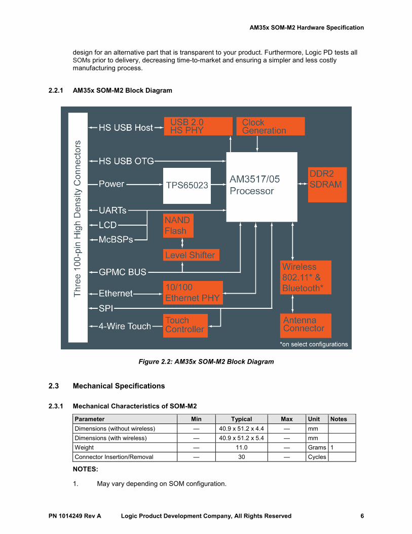
2.2.1 AM35x SOM-M2 Block Diagram
Figure 2.2: AM35x SOM-M2 Block Diagram
2.3 Mechanical Specifications
2.3.1 Mechanical Characteristics of SOM-M2
Parameter Min Typical Max Unit Notes Dimensions (without wireless) — 40.9 x 51.2 x 4.4 — mm Dimensions (with wireless) — 40.9 x 51.2 x 5.4 — mm Weight — 11.0 — Grams 1 Connector Insertion/Removal — 30 — Cycles
NOTES:
1. May vary depending on SOM configuration.
AM35x SOM-M2 Hardware Specification
PN 1014249 Rev A Logic Product Development Company, All Rights Reserved 7
2.3.2 Interface Connectors
The AM35x SOM-M2 connects to a PCB baseboard through three 100-pin board-to-board (BTB) socket connectors.
Table 2.1: Board-to-Board Socket Connectors Manufacturer Information
Ref Designator Manufacturer SOM-M2 Connector P/N Mating Connector P/N J1:3 Hirose DF40C-100DP-0.4V(51) DF40C-100DS-0.4V(51)
2.3.3 Wireless Antenna Connection
The mechanical drawing in Appendix A shows the location of the 802.11b/g/n Ethernet and Bluetooth antenna connector (J4) on the top side of the PCB. Table 2.2 contains the manufacturer information for the cables that Logic PD provides in the AM3517 EVM Development Kit.
NOTE: To comply with FCC certification already completed on the AM35x SOM-M2, the antenna selected for an end product must meet FCC guidelines as described in Section 3.7.1.
Table 2.2: Wireless Antenna Cable Manufacturer Information
Ref Designator Manufacturer P/N J4 Hirose U.FL Coax cable Sunridge Corp. MCBG-RH-54-080-SMAJB281
2.3.4 AM35x SOM-M2 Mechanical Drawings
Please see Appendix A for mechanical drawings of the AM35x SOM-M2 and recommended baseboard footprint layout.
2.3.5 Example AM35x SOM-M2 Retention Methods
Please see Appendix B for mechanical drawings demonstrating three possible retention methods for the AM35x SOM-M2. These drawings are only meant to serve as possible solutions and should not be considered final designs for retention.
2.4 Temperature Specifications Parameter Min Typical Max Unit Notes Commercial Operating Temperature 0 25 70 °C Industrial Operating Temperature -40 25 85 °C 1 Storage Temperature -40 25 85 °C
NOTES:
1. Industrial temperature model will be available in the second half of 2010. Industrial temperature model does not include Wi-Fi/Bluetooth module.
AM35x SOM-M2 Hardware Specification
PN 1014249 Rev A Logic Product Development Company, All Rights Reserved 8
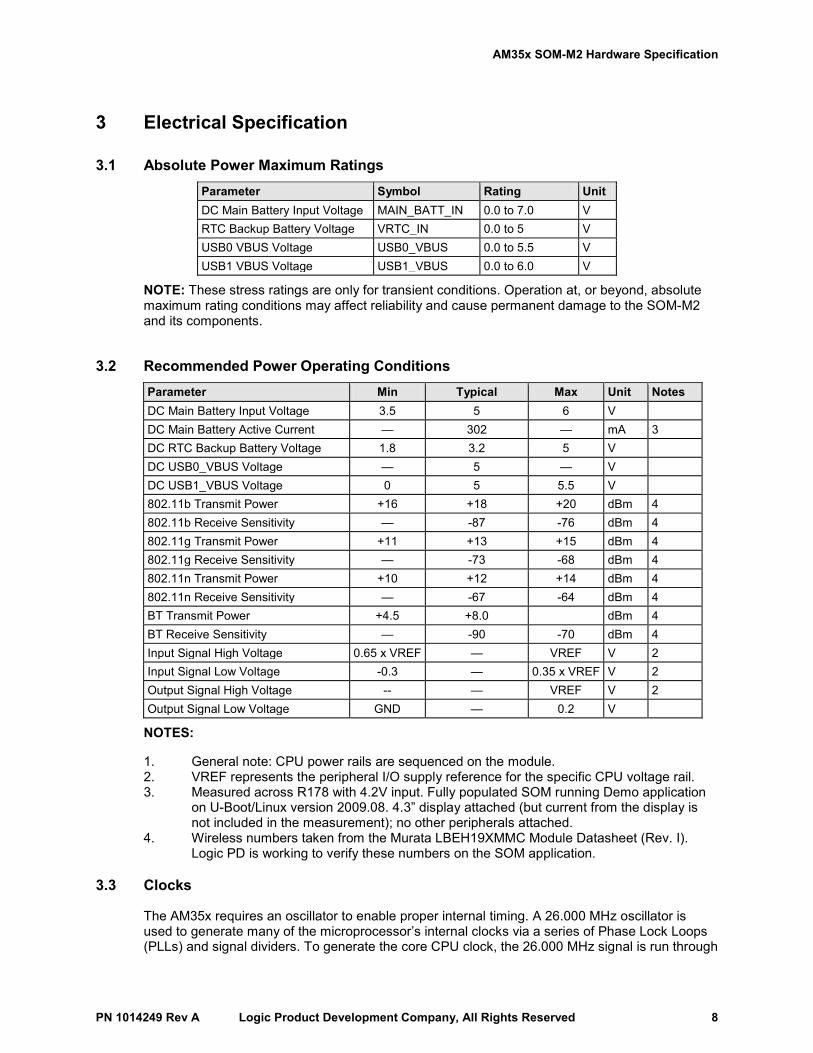
3 Electrical Specification
3.1 Absolute Power Maximum Ratings Parameter Symbol Rating Unit DC Main Battery Input Voltage MAIN_BATT_IN 0.0 to 7.0 V RTC Backup Battery Voltage VRTC_IN 0.0 to 5 V USB0 VBUS Voltage USB0_VBUS 0.0 to 5.5 V USB1 VBUS Voltage USB1_VBUS 0.0 to 6.0 V
NOTE: These stress ratings are only for transient conditions. Operation at, or beyond, absolute maximum rating conditions may affect reliability and cause permanent damage to the SOM-M2 and its components.
3.2 Recommended Power Operating Conditions Parameter Min Typical Max Unit Notes DC Main Battery Input Voltage 3.5 5 6 V DC Main Battery Active Current — 302 — mA 3 DC RTC Backup Battery Voltage 1.8 3.2 5 V DC USB0_VBUS Voltage — 5 — V DC USB1_VBUS Voltage 0 5 5.5 V 802.11b Transmit Power +16 +18 +20 dBm 4 802.11b Receive Sensitivity — -87 -76 dBm 4 802.11g Transmit Power +11 +13 +15 dBm 4 802.11g Receive Sensitivity — -73 -68 dBm 4 802.11n Transmit Power +10 +12 +14 dBm 4 802.11n Receive Sensitivity — -67 -64 dBm 4 BT Transmit Power +4.5 +8.0 dBm 4 BT Receive Sensitivity — -90 -70 dBm 4 Input Signal High Voltage 0.65 x VREF — VREF V 2 Input Signal Low Voltage -0.3 — 0.35 x VREF V 2 Output Signal High Voltage -- — VREF V 2 Output Signal Low Voltage GND — 0.2 V
NOTES:
1. General note: CPU power rails are sequenced on the module. 2. VREF represents the peripheral I/O supply reference for the specific CPU voltage rail. 3. Measured across R178 with 4.2V input. Fully populated SOM running Demo application
on U-Boot/Linux version 2009.08. 4.3” display attached (but current from the display is not included in the measurement); no other peripherals attached.
4. Wireless numbers taken from the Murata LBEH19XMMC Module Datasheet (Rev. I). Logic PD is working to verify these numbers on the SOM application.
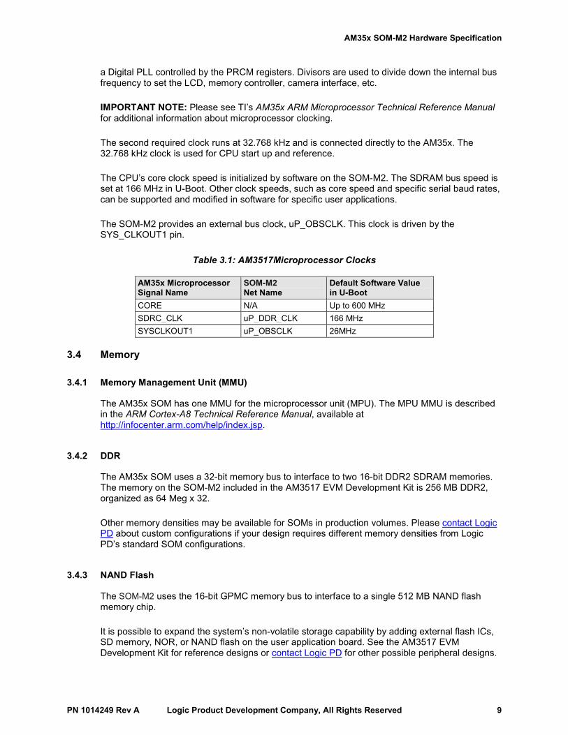
3.3 Clocks
The AM35x requires an oscillator to enable proper internal timing. A 26.000 MHz oscillator is used to generate many of the microprocessor’s internal clocks via a series of Phase Lock Loops (PLLs) and signal dividers. To generate the core CPU clock, the 26.000 MHz signal is run through
AM35x SOM-M2 Hardware Specification
PN 1014249 Rev A Logic Product Development Company, All Rights Reserved 9
a Digital PLL controlled by the PRCM registers. Divisors are used to divide down the internal bus frequency to set the LCD, memory controller, camera interface, etc.
IMPORTANT NOTE: Please see TI’s AM35x ARM Microprocessor Technical Reference Manual for additional information about microprocessor clocking.
The second required clock runs at 32.768 kHz and is connected directly to the AM35x. The 32.768 kHz clock is used for CPU start up and reference.
The CPU’s core clock speed is initialized by software on the SOM-M2. The SDRAM bus speed is set at 166 MHz in U-Boot. Other clock speeds, such as core speed and specific serial baud rates, can be supported and modified in software for specific user applications.
The SOM-M2 provides an external bus clock, uP_OBSCLK. This clock is driven by the SYS_CLKOUT1 pin.
Table 3.1: AM3517Microprocessor Clocks
AM35x Microprocessor Signal Name
SOM-M2 Net Name
Default Software Value in U-Boot
CORE N/A Up to 600 MHz SDRC_CLK uP_DDR_CLK 166 MHz SYSCLKOUT1 uP_OBSCLK 26MHz
3.4 Memory
3.4.1 Memory Management Unit (MMU)
The AM35x SOM has one MMU for the microprocessor unit (MPU). The MPU MMU is described in the ARM Cortex-A8 Technical Reference Manual, available at http://infocenter.arm.com/help/index.jsp.
3.4.2 DDR
The AM35x SOM uses a 32-bit memory bus to interface to two 16-bit DDR2 SDRAM memories. The memory on the SOM-M2 included in the AM3517 EVM Development Kit is 256 MB DDR2, organized as 64 Meg x 32.
Other memory densities may be available for SOMs in production volumes. Please contact Logic PD about custom configurations if your design requires different memory densities from Logic PD’s standard SOM configurations.
3.4.3 NAND Flash
The SOM-M2 uses the 16-bit GPMC memory bus to interface to a single 512 MB NAND flash memory chip.
It is possible to expand the system’s non-volatile storage capability by adding external flash ICs, SD memory, NOR, or NAND flash on the user application board. See the AM3517 EVM Development Kit for reference designs or contact Logic PD for other possible peripheral designs.
AM35x SOM-M2 Hardware Specification
PN 1014249 Rev A Logic Product Development Company, All Rights Reserved 10
3.4.4 MMC/SD Support
The SOM-M2 directly supports a single SD/MMC slot. The SOM-M2 routes the signals for MMC1 to the baseboard connectors, allowing connections on a user design to a socket where a card can be mounted. MMC1 supports up to 8 data bits. The AM35x microprocessor has functionality for two more MMC peripherals: MMC2 is used for the Murata Wi-Fi/Bluetooth module on the SOM. It has functionality on the upper 4 data bits to support direction control for an SD/MMC buffer. MMC3 is an alternate pin mapping for other peripherals used elsewhere on the SOM.
The AM3517 eXperimenter Board reference design includes a single SD/MMC connector. Please contact Logic PD for more information on implementing additional slots.
3.5 DMA The AM35x has several DMA controllers: ■ SDMA – data transfers from the microprocessor to peripherals ■ Display DMA ■ USB High Speed (HS) DMA The SDMA controller (DMA4) has the following features: ■ 32 channels (independent, concurrent, variable data size, burst/chain, endian conversion) ■ Memory to memory, memory to peripheral ■ Interrupts ■ 256 32-bit FIFOs
3.6 10/100 Ethernet PHY
The AM35x SOM-M2 uses an SMSC LAN8710 Ethernet PHY to provide an easy-to-use networking interface. The four analog PHY interface signals (transmit/receive) each require an external impedance matching circuit to operate properly. Logic PD provides an example circuit schematic in the AM35x eXperimenter Board Schematics. Please note the TX+/- and RX+/- pairs must be routed as differential pairs (at 100 ohms) on the baseboard PCB.
The 10/100 Ethernet MAC address can be found in two ways. One, the MAC address is printed on a sticker affixed to the top side of the SOM and is the address that does not follow this convention: 00:08:EE:xx:xx:xx. Two, the 10/100 Ethernet MAC address is stored within the AM35x microprocessor and can be obtained using software; please refer to TI’s AM35x ARM Microprocessor Technical Reference Manual for this procedure.
3.7 802.11 Wireless Ethernet + Bluetooth
The SOM-M2 uses a Murata LBEH19XMMC 802.11b/g/n + Bluetooth 2.1 Wireless IC to provide an easy-to-use wireless networking interface. The LBEH19XMMC is connected to the AM35x through a combination of MMC, SDIO, and GPIO. The RF connector is located on the SOM at reference designator J4; J4 is shared between 802.11 and Bluetooth.
The MAC address for 802.11b/g/n is printed on a sticker affixed to the top side of the SOM. The 802.11b/g/n MAC address follows this convention: 00:08:EE:xx:xx:xx
NOTE: Transmit power (VBAT) comes from U22, which converts the incoming voltage (MAIN_BATT_IN) to ~3.5V.
AM35x SOM-M2 Hardware Specification
PN 1014249 Rev A Logic Product Development Company, All Rights Reserved 11
NOTE: See Application Note 447 for FCC guidelines pertaining to use of the AM35x SOM-M2 in end products.
3.7.1 2.4 GHz Antenna Information
The AM35x SOM-M2 has been qualified to use a Pulse W1038, 4.9 dBi Omni-directional antenna. Use of this antenna will satisfy FCC regulations. A different Omni-directional antenna with a peak gain of 4.9 dBi or less may be substituted and still satisfy FCC regulations. If an antenna with higher gain or of a different type is to be used, the end product must be put through intentional radiation testing at a qualified test lab. Please refer to FCC rules 47 CFR § 15.204 for more information.
3.7.2 Software Requirements
In order to be FCC compliant with the 802.11b/g/n and Bluetooth devices, the following software must be used:
■ 802.11b/g/n: Firmware Version: Rev 6.1.0.0.313 ■ Bluetooth: Firmware Version: 7.2.31; initialization script TI_P31.91 Any other version of the firmware must be approved by the FCC. If another version of the firmware is desired, please contact Logic PD for assistance with certification.
3.7.3 FM Interface
The Murata module on the SOM-M2 has FM capabilities. FM signals are routed to the baseboard connectors (see Section 6) for connection to audio processing and antenna.
NOTE: The FM interface is untested and not supported with software.
IMPORTANT NOTE: The FCC certification for the AM35x SOM-M2 does not cover FM signals; therefore, use of FM signals will require independent FCC testing and certification.
3.8 Display Interface
The AM35x has a built-in graphics controller supporting up to 24-bit parallel RGB (pixel rates up to 74.25 MHz enabling HD resolutions) along with two 10-bit Digital-to-Analog Converters (DAC) supporting composite NTSC/PAL video and Luma/Chroma Separate Video (S-Video). Image rotation, resizing, color space conversion, and 8-bit alpha blending functions are built in. See TI’s AM35x Technical Reference Manual for further information on the integrated LCD controller.
The signals from the AM35x LCD controller are organized by bit and color and can be interfaced through the SOM-M2 expansion connectors. The signals from the SOM-M2 are driven from the 3.3V_or_1.8V rail. Logic PD has written drivers for panels of different types and sizes. Please contact Logic PD before selecting a display for your application.
NOTE: In 3.3V IO mode, an LCD can be driven directly from the AM3517.
NOTE: The eXperimenter Baseboard uses the standard Logic PD 16-bit LCD interface as well as a 24-bit HDMI transceiver.
AM35x SOM-M2 Hardware Specification
PN 1014249 Rev A Logic Product Development Company, All Rights Reserved 12
IMPORTANT NOTE: Using the internal graphics controller may affect microprocessor performance. Selecting display resolutions and color bits per pixel will vary microprocessor busload.
3.9 Video Processing Front End
The AM35x has a built-in 16-bit video input port supporting RAW data interface, up 75 MHz pixel clock, REC656/CCIR656, YCbCr422 format (8- and 16-bit), black clamping signal generation, 10-bit to 8-bit A-law compression, and up to 16K pixels in horizontal and vertical directions. The signal input to the VPFE is through the CCDC bus connections. The SOM-M2 supports an 8-bit video input interface with control lines on the CCDC bus (see Section 6). See TI’s AM35x Technical Reference Manual and Logic PD’s AM3517 Application Board Schematics for connection details.
3.9.1 TV_OUT
The AM35x supports S-Video on the TV_OUT signals (see Section 6 for details). Note that the TV_OUT signals need to be routed at 75 ohms single ended. There are optional noise-filtering component locations on the SOM-M2 for the TV_OUT signals.
3.10 Serial Interfaces
The SOM-M2 comes with the following serial channels: high end CAN controller, multichannel buffered serial ports (McBSPs), four McSPI ports, up to four UARTS, and three I2C ports. If additional serial channels are required, please contact Logic PD for reference designs. Please see TI’s AM35x Technical Reference Manual for further information regarding serial communications.
3.10.1 CAN Controller
The AM3517 has a high performance CAN 2.0B controller. It includes a CAN Protocol Kernel, a Standard CAN Controller (SCC), and a High End CAN Controller (HECC). The SCC supports 16 receive/transmit message objects, while the HECC supports 32 receive/transmit message objects. The HECC also supports 32 receive-identifier masks.
Other features of the CAN controller include:
■ 1 Mbps data rate ■ Programmable sampling rate ■ Selectable edge for synchronization ■ Automatic re-transmission ■ Bus failure diagnostic ■ Self test ■ Wake-up on bus activity ■ Auto reply The signals from the SOM-M2 are driven from the 3.3V_or_1.8V rail. The end-product design must provide an external CAN transceiver. Logic PD has provided an example reference design with the AM3517 Application Board Schematics. When choosing a CAN transceiver, the designer should keep in mind bus loading, availability, ESD protection, and data rates.
AM35x SOM-M2 Hardware Specification
PN 1014249 Rev A Logic Product Development Company, All Rights Reserved 13
3.10.2 McBSP
The SOM-M2 provides access to four multi-channel buffered serial ports (McBSP) with the following capabilities:
■ Full-duplex and multi-drop ■ 512B FIFO on McBSP1, 3, 4; 5KB FIFO on McBSP2 ■ Max data rate of 48 Mbps ■ I2S, PCM, and TDMI support ■ Support for external clocks and frame sync ■ Sidetone support on McBSP2/3 (requires channels are looped back) The signals from the SOM-M2 are scaled to IO voltage levels (3.3V_or_1.8V), not RS232 level signals.
NOTE: McBSP5 is an alternate pin mapping of the HSUSB bus. On the AM35x SOM-M2, uP_HSUSB is used for the USB host port and McBSP5 is not available.
3.10.3 UARTs
The AM35x microprocessor has up to four asynchronous serial ports with the following capabilities:
■ 16C750-compatible. ■ IrDA and CIR support (UART3 only) ■ 64 byte FIFO on receive and transmit ■ Hardware or software flow control ■ Baud rates to 3686400 bps The signals from the SOM-M2 are TTL level signals (3.3V_or_1.8V), not RS232 level signals.
NOTE: UART4 is an alternate pin function of GPMC_WAIT1/2.
3.10.4 McSPI
The SOM-M2 makes McSPI ports 1 and 2 available. They have the following characteristics:
■ Four channels / chip selects (McSPI1) ■ Two channels / chip selects (McSPI2) ■ Programmable frequency, polarity, and phase for each channel ■ SPI word lengths ranging from 4 bits to 32 bits ■ Up to four master channels or single channel in slave mode ■ Master multichannel mode with either full duplex or half duplex ■ 64 byte FIFO Please see TI’s AM35xx Technical Reference Manual for further information. The signals from the SOM-M2 are TTL level signals (3.3V or 1.8V), not RS232 level signals. Note that McSPI3 is an alternate function of MMC2, which is used for the on-board Murata WiFi module.
3.10.5 I2C
The AM35x microprocessor has three I2C ports with the following characteristics:
■ Slave or master mode ■ Serial camera control bus (SCCB) mode ■ Compliant with I2C version 2.1
AM35x SOM-M2 Hardware Specification
PN 1014249 Rev A Logic Product Development Company, All Rights Reserved 14
■ Standard (100Kbps) and fast mode (400Kbps) ■ High-speed mode up to 3.4Mbps ■ 7- and 10-bit addressing ■ 8 byte (I2C1, I2C2) and 64 byte (I2C3) FIFOs Please see TI’s AM35x ARM Microprocessor Technical Reference Manual for further information. The signals from the SOM-M2 are TTL level signals (3.3V or 1.8V), not RS232 level signals.
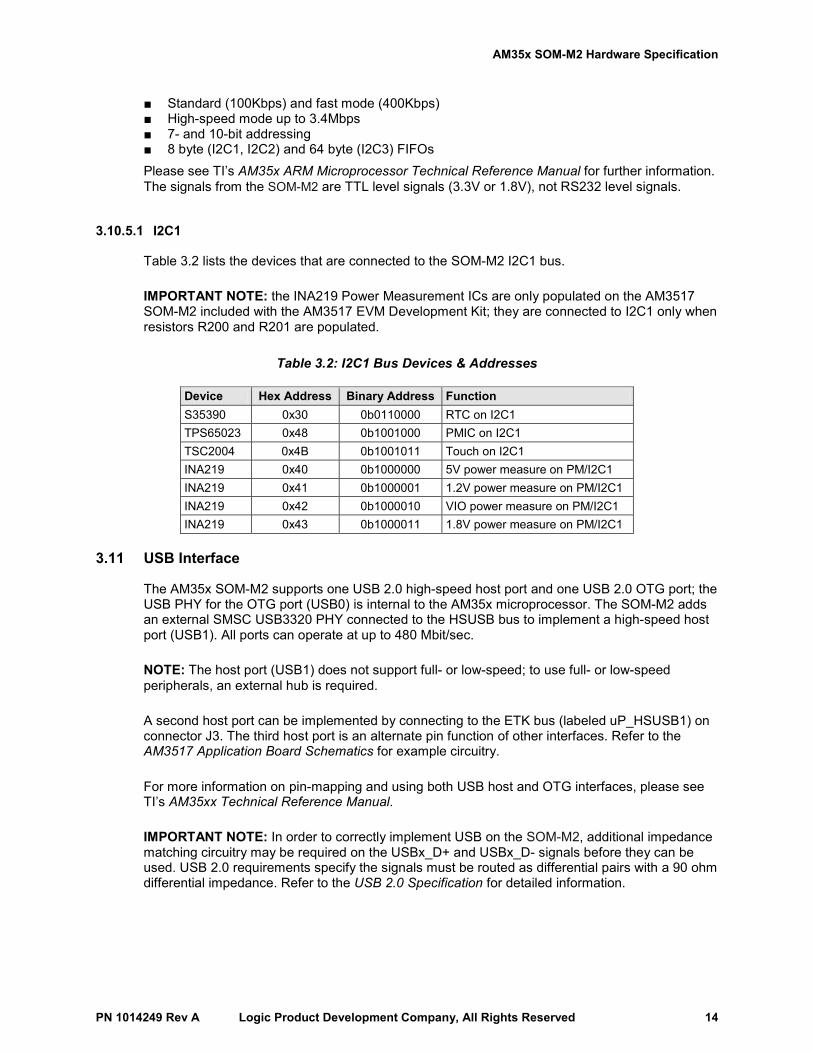
3.10.5.1 I2C1
Table 3.2 lists the devices that are connected to the SOM-M2 I2C1 bus.
IMPORTANT NOTE: the INA219 Power Measurement ICs are only populated on the AM3517 SOM-M2 included with the AM3517 EVM Development Kit; they are connected to I2C1 only when resistors R200 and R201 are populated.
Table 3.2: I2C1 Bus Devices & Addresses
Device Hex Address Binary Address Function S35390 0x30 0b0110000 RTC on I2C1 TPS65023 0x48 0b1001000 PMIC on I2C1 TSC2004 0x4B 0b1001011 Touch on I2C1 INA219 0x40 0b1000000 5V power measure on PM/I2C1 INA219 0x41 0b1000001 1.2V power measure on PM/I2C1 INA219 0x42 0b1000010 VIO power measure on PM/I2C1 INA219 0x43 0b1000011 1.8V power measure on PM/I2C1
3.11 USB Interface
The AM35x SOM-M2 supports one USB 2.0 high-speed host port and one USB 2.0 OTG port; the USB PHY for the OTG port (USB0) is internal to the AM35x microprocessor. The SOM-M2 adds an external SMSC USB3320 PHY connected to the HSUSB bus to implement a high-speed host port (USB1). All ports can operate at up to 480 Mbit/sec.
NOTE: The host port (USB1) does not support full- or low-speed; to use full- or low-speed peripherals, an external hub is required.
A second host port can be implemented by connecting to the ETK bus (labeled uP_HSUSB1) on connector J3. The third host port is an alternate pin function of other interfaces. Refer to the AM3517 Application Board Schematics for example circuitry.
For more information on pin-mapping and using both USB host and OTG interfaces, please see TI’s AM35xx Technical Reference Manual.
IMPORTANT NOTE: In order to correctly implement USB on the SOM-M2, additional impedance matching circuitry may be required on the USBx_D+ and USBx_D- signals before they can be used. USB 2.0 requirements specify the signals must be routed as differential pairs with a 90 ohm differential impedance. Refer to the USB 2.0 Specification for detailed information.
AM35x SOM-M2 Hardware Specification
PN 1014249 Rev A Logic Product Development Company, All Rights Reserved 15
3.12 ADC/Touch Interface
The SOM-M2 uses TI’s TSC2004 touch screen controller (TSC). The controller includes a 12-bit analog-to-digital converter (ADC). This TSC is used to support standard 4-wire resistive touch panels and one auxiliary A/D signal. The device is connected to the CPU by the I2C1 interface. Please see TI’s TSC2004 Datasheet for more information.
3.13 Real Time Clock (RTC)
The SOM-M2 has a Seiko S35390 real time clock connected to I2C1. Note that the RTC requires an additional voltage (VRTC_IN) to operate and to perform timekeeping when MAIN_BATT_IN is not present.
The voltage for the RTC comes from VRTC_IN (see Section 6). The AM3517 EVM Development Kit reference design includes example circuitry to power VRTC_IN from either the power supply or backup battery.
3.14 General Purpose I/O (GPIO)
Logic PD designed the SOM-M2 to be flexible and provide multiple options for analog and digital GPIO. There are numerous digital GPIO pins on the SOM-M2 that interface to the AM35x. See Section 6 of this document for more information. If certain peripherals are not desired, such as the LCD controller, chip selects, or UARTs, then more GPIO pins become available.
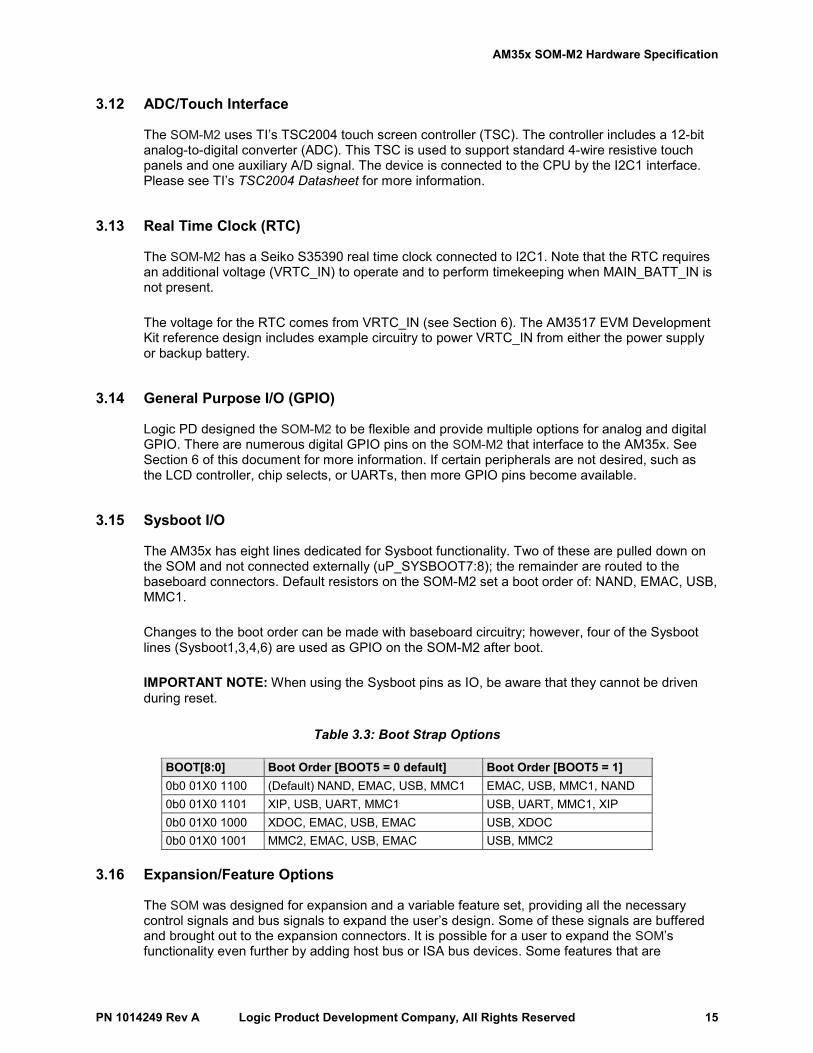
3.15 Sysboot I/O
The AM35x has eight lines dedicated for Sysboot functionality. Two of these are pulled down on the SOM and not connected externally (uP_SYSBOOT7:8); the remainder are routed to the baseboard connectors. Default resistors on the SOM-M2 set a boot order of: NAND, EMAC, USB, MMC1.
Changes to the boot order can be made with baseboard circuitry; however, four of the Sysboot lines (Sysboot1,3,4,6) are used as GPIO on the SOM-M2 after boot.
IMPORTANT NOTE: When using the Sysboot pins as IO, be aware that they cannot be driven during reset.
Table 3.3: Boot Strap Options
BOOT[8:0] Boot Order [BOOT5 = 0 default] Boot Order [BOOT5 = 1] 0b0 01X0 1100 (Default) NAND, EMAC, USB, MMC1 EMAC, USB, MMC1, NAND 0b0 01X0 1101 XIP, USB, UART, MMC1 USB, UART, MMC1, XIP 0b0 01X0 1000 XDOC, EMAC, USB, EMAC USB, XDOC 0b0 01X0 1001 MMC2, EMAC, USB, EMAC USB, MMC2
3.16 Expansion/Feature Options
The SOM was designed for expansion and a variable feature set, providing all the necessary control signals and bus signals to expand the user’s design. Some of these signals are buffered and brought out to the expansion connectors. It is possible for a user to expand the SOM’s functionality even further by adding host bus or ISA bus devices. Some features that are

AM35x SOM-M2 Hardware Specification
PN 1014249 Rev A Logic Product Development Company, All Rights Reserved 16
implemented on the AM35x microprocessor, but are not discussed herein, include: pulse width modulation (PWM), Secure Digital, MMC cards, SDIO cards, 1wire interface, watchdog timers, or the debug module. See TI’s AM35xx Technical Reference Manual and Logic PD’s AM3517 SOM-M2 Schematics for more details. Logic PD has experience implementing additional options, including other audio codecs, Ethernet ICs, co-processors, and components on SOMs. Please contact Logic PD for potential reference designs before selecting your peripherals.
AM35x SOM-M2 Hardware Specification
PN 1014249 Rev A Logic Product Development Company, All Rights Reserved 17
4 System Integration
4.1 Custom Configuration
The AM3517 SOM-M2 was designed to meet multiple applications for users with specific design and budget requirements. As a result, this SOM supports a variety of embedded operating systems, flexible DDR and flash memory footprints, and other hardware configurations. If your application needs require unique hardware or software configurations, please contact Logic PD about custom SOMs available in production volumes.
4.2 Resets
The SOM-M2 has a reset input (RESPWRONn) and a reset output (RESOUTn). External devices should use RESPWRONn to assert reset to the product. The SOM-M2 uses RESOUTn to indicate to other devices that the SOM-M2 is in reset.
4.2.1 Master Reset (RESPWRONn)—Reset Input
Logic PD suggests that custom designs implementing the AM35x SOM-M2 use the RESPWRONn signal as the “pin-hole” reset used in commercial embedded systems. The RESPWRONn triggers a power-on-reset event to the AM35x microprocessor via the TPS65023 PMIC and resets the entire CPU.
IMPORTANT NOTE: Any custom reset circuit design should guard the assertion of the reset lines during a low power state so as to prevent power-up in a low or bad power condition. (Powering up in a low or bad power condition will cause data corruption and, possibly, temporary system lock. Either one of the following two conditions will cause a system-wide reset: power on the RESPWRONn signal or a low pulse on the RESPWRONn signal.
Low Pulse on RESPWRONn Signal
A low pulse on the RESPWRONn signal for longer than 30mS—asserted by an external source (for example, the reset button on the custom design application)—will bring RESOUTn low for 100mS after the assertion source is de-asserted.
Logic PD suggests that for any external assertion source that triggers the RESPWRONn signal, analog or digital, de-bouncing should be used to generate a clean, one-shot reset signal.
4.2.2 SOM-M2 Reset (RESOUTn)—Reset Output
All hardware peripherals should connect their hardware-reset pin to the RESOUTn signal on the expansion connector. Internally, all SOM-M2 peripheral hardware reset pins are connected to the RESOUTn net.
If the reset circuit is asserted (active low), the user can expect to lose information stored in RAM. The data loss occurs because the CPU is reset to its reset defaults.
AM35x SOM-M2 Hardware Specification
PN 1014249 Rev A Logic Product Development Company, All Rights Reserved 18
4.2.3 SOM-M2 Reset (uP_RESWARMn)—Reset Input/Output
uP_RESWARMn is the raw AM35x reset I/O. As such, it is sensitive to external loading and no devices with active pull-ups should be added to this line. It is permissible to have active low circuitry on this line.
4.3 Interrupts
The AM35x incorporates the ARM Cortex-A8 interrupt controller which provides many inter-system interrupt sources and destinations. Most external GPIO signals can also be configured as interrupt inputs by configuring their pin control registers. Logic PD BSPs setup and process all SOM-M2 interrupt sources, onboard and external. Refer to TI’s AM35xx Reference Manual for further information on using interrupts. IRQn is routed to the baseboard, see Section 6 for details.
4.4 JTAG Debugger Interface
The JTAG connection on the AM35x allows recovery of corrupted flash memory, and real-time application debug. There are several third-party JTAG debuggers available for TI microprocessors. The following signals make up the JTAG interface to the AM35x microprocessor: TDI, TMS, TCK, TDO, nTRST, RTCK, EMU0, EMU1, and RESOUTn (RESOUTn is only required for some JTAG tools; see the JTAG tool documentation for exact pinout). These signals should interface directly to a 20-pin 0.1” through-hole connector, as shown on the AM3517 eXperimenter Baseboard Schematics.
IMPORTANT NOTE: When laying out the 20-pin connector, realize that it may not be numbered as a standard 20-pin 0.1” insulation displacement connector (IDC) through-hole connector. See the EVM Development Kit reference design for further details. Each JTAG tool vendor may define the 20-pin IDC connector pin-out differently.
4.5 Power Management
4.5.1 System Power Supplies
In order to ensure a flexible design, the SOM-M2 has the following power inputs: MAIN_BATT_IN and VRTC. MAIN_BATT_IN is the power input to the SOM-M2 PMIC (TPS65023). The TPS65023 generates the on-board voltages for the AM35x and associated peripherals.
Note that 3.3V_or_1.8V is an output of the SOM PMIC, and is the selectable IO voltage rail. The setting is determined by the baseboard design by using signal IO_VOLTAGE_SEL (see Section 6 for details).
IMPORTANT NOTE: 3.3V_or_1.8V is an output from the SOM-M2, and should only be used as a reference voltage input to level shifting devices on baseboard designs.
4.5.1.1 MAIN_BATT_IN
The MAIN_BATT_IN input is the main source of power for the SOM-M2. In normal configuration, this input expects a voltage from 3.5V to 5V. The TPS65023 power management controller takes the MAIN_BATT_IN rail input and creates all onboard voltages. If the design is required to maintain RAM contents in a critical power situation (e.g., low battery, loss of power), the
AM35x SOM-M2 Hardware Specification
PN 1014249 Rev A Logic Product Development Company, All Rights Reserved 19
MAIN_BATT_IN supply should be maintained above the minimum level at all costs (see Section 2).
4.5.1.2 VRTC_IN
VRTC_IN is used to power the real time clock, U35. Always power this rail to maintain the clock and power state of the product. A lithium-ion coin cell typically supplies power to this rail. See the AM3517 eXperimenter Baseboard Schematic for details on powering VRTC_IN.
4.5.2 Dual Voltage I/O
The AM35x microprocessor and SOM-M2 uniquely support dual-voltage I/O. The user may select an operating voltage of either 1.8V or 3.3V through “IO_VOLTAGE_SEL” J1.37. For 3.3V operation, J1.37 should be left unconnected. For 1.8V operation, J1.37 should be tied directly to GND.
IMPORTANT NOTE: The IO_VOLTAGE_SEL line should only be changed with the SOM powered off.
4.5.3 System Power Management
Good power management design is important in any system development and embedded system design is no exception. In embedded system design, power management is typically one of the most complicated areas due to the dramatic effect it has on product cost, performance, usability, and overall customer satisfaction. Many factors affect a power-efficient hardware design: power supply selection (efficiency), clocking design, IC and component selection, etc. The SOM was designed with these aspects in mind while also providing maximum flexibility in software and system integration.
On the AM35x there are many different software configurations that drastically affect power consumption: microprocessor core clock frequency, bus clock frequency, peripheral clocks, bus modes, power management states; peripheral power states and modes; product user scenarios; interrupt handling; and display settings (resolution, backlight, refresh, bits per pixel, etc). These settings are typically initialized in the startup software routines and may be modified later in the operating system and application software. Information for these items can be found in the appropriate documents such as the U-Boot User’s Manual or the specific BSP manual.
4.5.4 System Power Sequencing
Power sequencing for the AM35x is handled by the TPS65023 PMIC.
IMPORTANT NOTE: External circuitry should guarantee that any voltages applied to SOM pins are present only after the SOM-M2 has completed its power up sequence. Failure to do so may result in erratic SOM-M2 operation or device damage. One way to ensure this is to use the external reset (RESOUTn) as a gating signal for all external power supplies.
4.6 ESD Considerations
The SOM was designed to interface to a customer’s peripheral board, while remaining low cost and adaptable to many different applications. The SOM does not provide any onboard ESD protection circuitry—this must be provided by the product it is used in. Logic PD has extensive
AM35x SOM-M2 Hardware Specification
PN 1014249 Rev A Logic Product Development Company, All Rights Reserved 20
experience in designing products with ESD requirements. Please contact Logic PD if you need any assistance in ESD design considerations.
AM35x SOM-M2 Hardware Specification
PN 1014249 Rev A Logic Product Development Company, All Rights Reserved 21
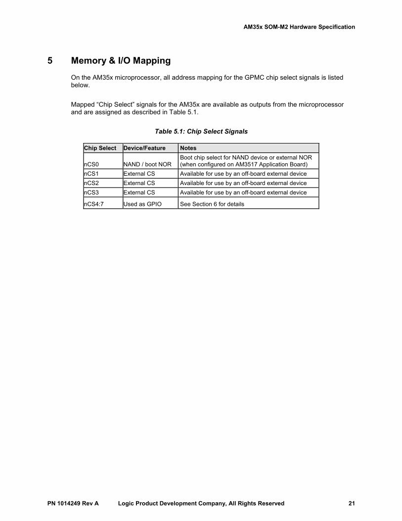
5 Memory & I/O Mapping
On the AM35x microprocessor, all address mapping for the GPMC chip select signals is listed below.
Mapped “Chip Select” signals for the AM35x are available as outputs from the microprocessor and are assigned as described in Table 5.1.
Table 5.1: Chip Select Signals
Chip Select Device/Feature Notes
nCS0 NAND / boot NOR Boot chip select for NAND device or external NOR (when configured on AM3517 Application Board)
nCS1 External CS Available for use by an off-board external device nCS2 External CS Available for use by an off-board external device nCS3 External CS Available for use by an off-board external device
nCS4:7 Used as GPIO See Section 6 for details
AM35x SOM-M2 Hardware Specification
PN 1014249 Rev A Logic Product Development Company, All Rights Reserved 22
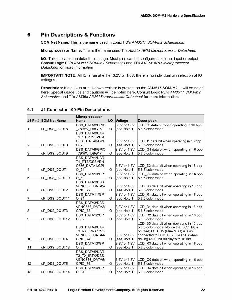
6 Pin Descriptions & Functions SOM Net Name: This is the name used in Logic PD’s AM3517 SOM-M2 Schematics.
Microprocessor Name: This is the name used TI’s AM35x ARM Microprocessor Datasheet.
I/O: This indicates the default pin usage. Most pins can be configured as either input or output. Consult Logic PD’s AM3517 SOM-M2 Schematics and TI’s AM35x ARM Microprocessor Datasheet for more information.
IMPORTANT NOTE: All IO is run at either 3.3V or 1.8V; there is no individual pin selection of IO voltages.
Description: If a pull-up or pull-down resistor is present on the AM3517 SOM-M2, it will be noted here. Special usage tips and cautions will be noted here. Consult Logic PD’s AM3517 SOM-M2 Schematics and TI’s AM35x ARM Microprocessor Datasheet for more information.
6.1 J1 Connector 100-Pin Descriptions
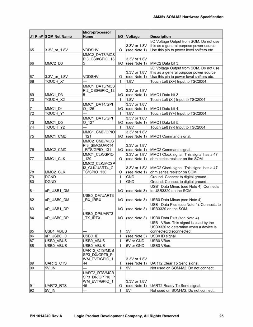
J1 Pin# SOM Net Name Microprocessor Name I/O Voltage Description
1 uP_DSS_DOUT8 DSS_DATA8/GPIO_78/HW_DBG16 O
3.3V or 1.8V (see Note 1)
LCD G3 data bit when operating in 16 bpp 5:6:5 color mode.
2 uP_DSS_DOUT0
DSS_DATA0/UART1_CTS/DSSVENC656_DATA0/GPIO_70 O
3.3V or 1.8V (see Note 1)
LCD B1 data bit when operating in 16 bpp 5:6:5 color mode.
3 uP_DSS_DOUT9 DSS_DATA9/GPIO_79/HW_DBG17 O
3.3V or 1.8V (see Note 1)
LCD_G4 data bit when operating in 16 bpp 5:6:5 color mode.
4 uP_DSS_DOUT1
DSS_DATA1/UART1_RTS/DSSVENC656_DATA1/GPIO_71 O
3.3V or 1.8V (see Note 1)
LCD_B2 data bit when operating in 16 bpp 5:6:5 color mode.
5 uP_DSS_DOUT10 DSS_DATA10/GPIO_80 O
3.3V or 1.8V (see Note 1)
LCD_G5 data bit when operating in 16 bpp 5:6:5 color mode.
6 uP_DSS_DOUT2
DSS_DATA2/DSSVENC656_DATA2/GPIO_72 O
3.3V or 1.8V (see Note 1)
LCD_B3 data bit when operating in 16 bpp 5:6:5 color mode.
7 uP_DSS_DOUT11 DSS_DATA11/GPIO_81 O
3.3V or 1.8V (see Note 1)
LCD_R1 data bit when operating in 16 bpp 5:6:5 color mode.
8 uP_DSS_DOUT3
DSS_DATA3/DSSVENC656_DATA3/GPIO_73 O
3.3V or 1.8V (see Note 1)
LCD_B4 data bit when operating in 16 bpp 5:6:5 color mode.
9 uP_DSS_DOUT12 DSS_DATA12/GPIO_82 O
3.3V or 1.8V (see Note 1)
LCD_R2 data bit when operating in 16 bpp 5:6:5 color mode.
10 uP_DSS_DOUT4
DSS_DATA4/UART3_RX_IRRX/DSSVENC656_DATA4/GPIO_74 O
3.3V or 1.8V (see Note 1)
LCD_B5 data bit when operating in 16 bpp 5:6:5 color mode. Notice that LCD_B0 is omitted; LCD_B5 (Blue MSB) is also connected to LCD_B0 (Blue LSB) when driving an 18 bit display with 16 bits.
11 uP_DSS_DOUT13 DSS_DATA13/GPIO_83 O
3.3V or 1.8V (see Note 1)
LCD_R3 data bit when operating in 16 bpp 5:6:5 color mode.
12 uP_DSS_DOUT5
DSS_DATA5/UART3_TX_IRTX/DSSVENC656_DATA5/GPIO_75 O
3.3V or 1.8V (see Note 1)
LCD_G0 data bit when operating in 16 bpp 5:6:5 color mode.
13 uP_DSS_DOUT14 DSS_DATA14/GPIO_84 O
3.3V or 1.8V (see Note 1)
LCD_R4 data bit when operating in 16 bpp 5:6:5 color mode.
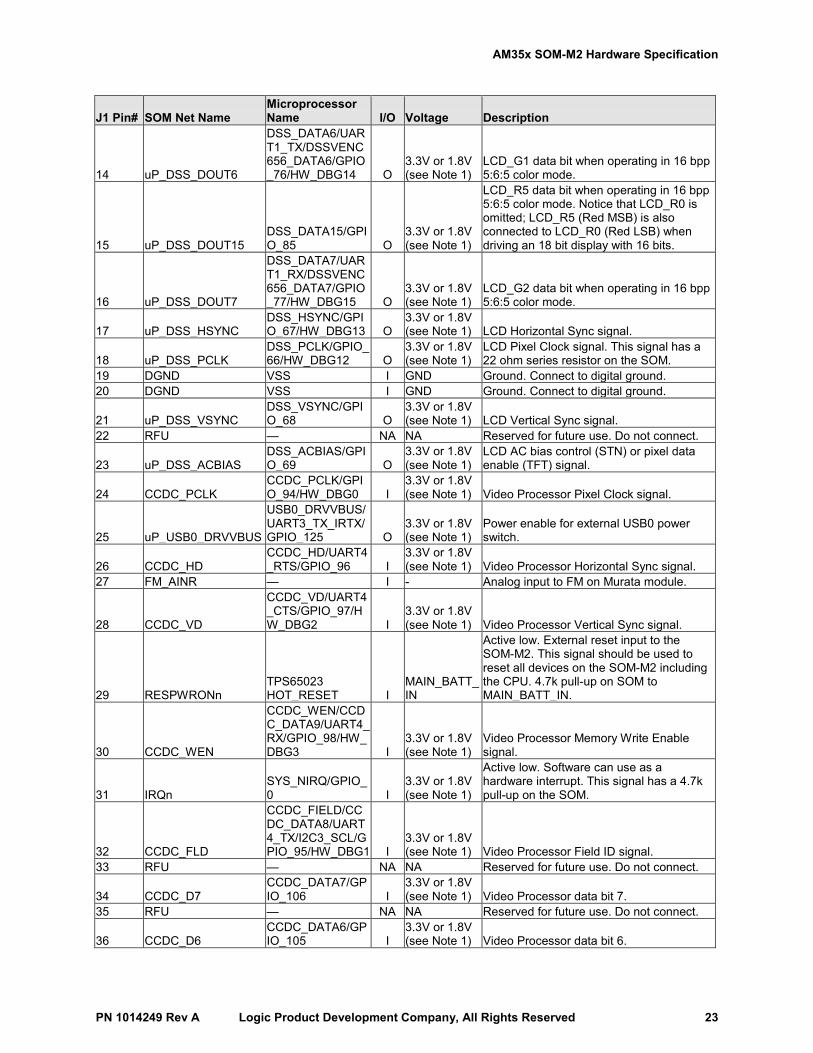
AM35x SOM-M2 Hardware Specification
PN 1014249 Rev A Logic Product Development Company, All Rights Reserved 23
J1 Pin# SOM Net Name Microprocessor Name I/O Voltage Description
14 uP_DSS_DOUT6
DSS_DATA6/UART1_TX/DSSVENC656_DATA6/GPIO_76/HW_DBG14 O
3.3V or 1.8V (see Note 1)
LCD_G1 data bit when operating in 16 bpp 5:6:5 color mode.
15 uP_DSS_DOUT15 DSS_DATA15/GPIO_85 O
3.3V or 1.8V (see Note 1)
LCD_R5 data bit when operating in 16 bpp 5:6:5 color mode. Notice that LCD_R0 is omitted; LCD_R5 (Red MSB) is also connected to LCD_R0 (Red LSB) when driving an 18 bit display with 16 bits.
16 uP_DSS_DOUT7
DSS_DATA7/UART1_RX/DSSVENC656_DATA7/GPIO_77/HW_DBG15 O
3.3V or 1.8V (see Note 1)
LCD_G2 data bit when operating in 16 bpp 5:6:5 color mode.
17 uP_DSS_HSYNC DSS_HSYNC/GPIO_67/HW_DBG13 O
3.3V or 1.8V (see Note 1) LCD Horizontal Sync signal.
18 uP_DSS_PCLK DSS_PCLK/GPIO_66/HW_DBG12 O
3.3V or 1.8V (see Note 1)
LCD Pixel Clock signal. This signal has a 22 ohm series resistor on the SOM.
19 DGND VSS I GND Ground. Connect to digital ground. 20 DGND VSS I GND Ground. Connect to digital ground.
21 uP_DSS_VSYNC DSS_VSYNC/GPIO_68 O
3.3V or 1.8V (see Note 1) LCD Vertical Sync signal.
22 RFU — NA NA Reserved for future use. Do not connect.
23 uP_DSS_ACBIAS DSS_ACBIAS/GPIO_69 O
3.3V or 1.8V (see Note 1)
LCD AC bias control (STN) or pixel data enable (TFT) signal.
24 CCDC_PCLK CCDC_PCLK/GPIO_94/HW_DBG0 I
3.3V or 1.8V (see Note 1) Video Processor Pixel Clock signal.
25 uP_USB0_DRVVBUS
USB0_DRVVBUS/UART3_TX_IRTX/GPIO_125 O
3.3V or 1.8V (see Note 1)
Power enable for external USB0 power switch.
26 CCDC_HD CCDC_HD/UART4_RTS/GPIO_96 I
3.3V or 1.8V (see Note 1) Video Processor Horizontal Sync signal.
27 FM_AINR — I - Analog input to FM on Murata module.
28 CCDC_VD
CCDC_VD/UART4_CTS/GPIO_97/HW_DBG2 I
3.3V or 1.8V (see Note 1) Video Processor Vertical Sync signal.
29 RESPWRONn TPS65023 HOT_RESET I
MAIN_BATT_IN
Active low. External reset input to the SOM-M2. This signal should be used to reset all devices on the SOM-M2 including the CPU. 4.7k pull-up on SOM to MAIN_BATT_IN.
30 CCDC_WEN
CCDC_WEN/CCDC_DATA9/UART4_RX/GPIO_98/HW_DBG3 I
3.3V or 1.8V (see Note 1)
Video Processor Memory Write Enable signal.
31 IRQn SYS_NIRQ/GPIO_0 I
3.3V or 1.8V (see Note 1)
Active low. Software can use as a hardware interrupt. This signal has a 4.7k pull-up on the SOM.
32 CCDC_FLD
CCDC_FIELD/CCDC_DATA8/UART4_TX/I2C3_SCL/GPIO_95/HW_DBG1 I
3.3V or 1.8V (see Note 1) Video Processor Field ID signal.
33 RFU — NA NA Reserved for future use. Do not connect.
34 CCDC_D7 CCDC_DATA7/GPIO_106 I
3.3V or 1.8V (see Note 1) Video Processor data bit 7.
35 RFU — NA NA Reserved for future use. Do not connect.
36 CCDC_D6 CCDC_DATA6/GPIO_105 I
3.3V or 1.8V (see Note 1) Video Processor data bit 6.
AM35x SOM-M2 Hardware Specification
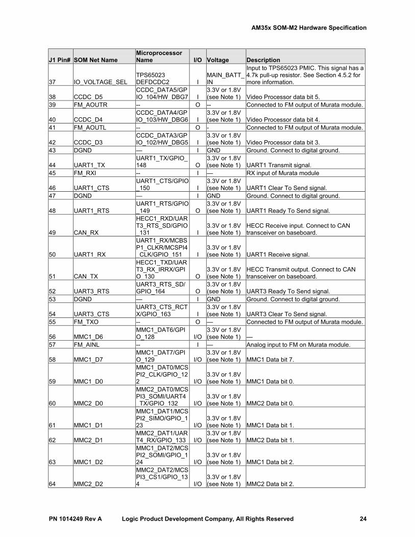
PN 1014249 Rev A Logic Product Development Company, All Rights Reserved 24
J1 Pin# SOM Net Name Microprocessor Name I/O Voltage Description
37 IO_VOLTAGE_SEL TPS65023 DEFDCDC2 I
MAIN_BATT_IN
Input to TPS65023 PMIC. This signal has a 4.7k pull-up resistor. See Section 4.5.2 for more information.
38 CCDC_D5 CCDC_DATA5/GPIO_104/HW_DBG7 I
3.3V or 1.8V (see Note 1) Video Processor data bit 5.
39 FM_AOUTR -- O -- Connected to FM output of Murata module.
40 CCDC_D4 CCDC_DATA4/GPIO_103/HW_DBG6 I
3.3V or 1.8V (see Note 1) Video Processor data bit 4.
41 FM_AOUTL -- O - Connected to FM output of Murata module.
42 CCDC_D3 CCDC_DATA3/GPIO_102/HW_DBG5 I
3.3V or 1.8V (see Note 1) Video Processor data bit 3.
43 DGND — I GND Ground. Connect to digital ground.
44 UART1_TX UART1_TX/GPIO_148 O
3.3V or 1.8V (see Note 1) UART1 Transmit signal.
45 FM_RXI -- I — RX input of Murata module
46 UART1_CTS UART1_CTS/GPIO_150 I
3.3V or 1.8V (see Note 1) UART1 Clear To Send signal.
47 DGND — I GND Ground. Connect to digital ground.
48 UART1_RTS UART1_RTS/GPIO_149 O
3.3V or 1.8V (see Note 1) UART1 Ready To Send signal.
49 CAN_RX
HECC1_RXD/UART3_RTS_SD/GPIO_131 I
3.3V or 1.8V (see Note 1)
HECC Receive input. Connect to CAN transceiver on baseboard.
50 UART1_RX
UART1_RX/MCBSP1_CLKR/MCSPI4_CLK/GPIO_151 I
3.3V or 1.8V (see Note 1) UART1 Receive signal.
51 CAN_TX
HECC1_TXD/UART3_RX_IRRX/GPIO_130 O
3.3V or 1.8V (see Note 1)
HECC Transmit output. Connect to CAN transceiver on baseboard.
52 UART3_RTS UART3_RTS_SD/GPIO_164 O
3.3V or 1.8V (see Note 1) UART3 Ready To Send signal.
53 DGND — I GND Ground. Connect to digital ground.
54 UART3_CTS UART3_CTS_RCTX/GPIO_163 I
3.3V or 1.8V (see Note 1) UART3 Clear To Send signal.
55 FM_TXO -- O — Connected to FM output of Murata module.
56 MMC1_D6 MMC1_DAT6/GPIO_128 I/O
3.3V or 1.8V (see Note 1) —
57 FM_AINL -- I — Analog input to FM on Murata module.
58 MMC1_D7 MMC1_DAT7/GPIO_129 I/O
3.3V or 1.8V (see Note 1) MMC1 Data bit 7.
59 MMC1_D0
MMC1_DAT0/MCSPI2_CLK/GPIO_122 I/O
3.3V or 1.8V (see Note 1) MMC1 Data bit 0.
60 MMC2_D0
MMC2_DAT0/MCSPI3_SOMI/UART4_TX/GPIO_132 I/O
3.3V or 1.8V (see Note 1) MMC2 Data bit 0.
61 MMC1_D1
MMC1_DAT1/MCSPI2_SIMO/GPIO_123 I/O
3.3V or 1.8V (see Note 1) MMC1 Data bit 1.
62 MMC2_D1 MMC2_DAT1/UART4_RX/GPIO_133 I/O
3.3V or 1.8V (see Note 1) MMC2 Data bit 1.
63 MMC1_D2
MMC1_DAT2/MCSPI2_SOMI/GPIO_124 I/O
3.3V or 1.8V (see Note 1) MMC1 Data bit 2.
64 MMC2_D2
MMC2_DAT2/MCSPI3_CS1/GPIO_134 I/O
3.3V or 1.8V (see Note 1) MMC2 Data bit 2.
AM35x SOM-M2 Hardware Specification
PN 1014249 Rev A Logic Product Development Company, All Rights Reserved 25
J1 Pin# SOM Net Name Microprocessor Name I/O Voltage Description
65 3.3V_or_1.8V VDDSHV O 3.3V or 1.8V (see Note 1)
I/O Voltage Output from SOM. Do not use this as a general purpose power source. Use this pin to power level shifters etc.
66 MMC2_D3
MMC2_DAT3/MCSPI3_CS0/GPIO_135 I/O
3.3V or 1.8V (see Note 1) MMC2 Data bit 3.
67 3.3V_or_1.8V VDDSHV O 3.3V or 1.8V (see Note 1)
I/O Voltage Output from SOM. Do not use this as a general purpose power source. Use this pin to power level shifters etc.
68 TOUCH_X1 — I 1.8V Touch Left (X+) Input to TSC2004.
69 MMC1_D3
MMC1_DAT3/MCSPI2_CS0/GPIO_125 I/O
3.3V or 1.8V (see Note 1) MMC1 Data bit 3.
70 TOUCH_X2 — I 1.8V Touch Left (X-) Input to TSC2004.
71 MMC1_D4 MMC1_DAT4/GPIO_126 I/O
3.3V or 1.8V (see Note 1) MMC1 Data bit 4.
72 TOUCH_Y1 — I 1.8V Touch Left (Y+) Input to TSC2004.
73 MMC1_D5 MMC1_DAT5/GPIO_127 I/O
3.3V or 1.8V (see Note 1) MMC1 Data bit 5.
74 TOUCH_Y2 — I 1.8V Touch Left (Y-) Input to TSC2004.
75 MMC1_CMD MMC1_CMD/GPIO_121 I/O
3.3V or 1.8V (see Note 1) MMC1 Command signal.
76 MMC2_CMD
MMC2_CMD/MCSPI3_SIMO/UART4_RTS/GPIO_131 I/O
3.3V or 1.8V (see Note 1) MMC2 Command signal.
77 MMC1_CLK MMC1_CLK/GPIO_120 O
3.3V or 1.8V (see Note 1)
MMC1 Clock signal. This signal has a 47 ohm series resistor on the SOM.
78 MMC2_CLK
MMC2_CLK/MCSPI3_CLK/UART4_CTS/GPIO_130 O
3.3V or 1.8V (see Note 1)
MMC2 Clock signal. This signal has a 47 ohm series resistor on SOM.
79 DGND — I GND Ground. Connect to digital ground. 80 DGND — I GND Ground. Connect to digital ground.
81 uP_USB1_DM -- I/O (see Note 3) USB1 Data Minus (see Note 4). Connects to USB3320 on the SOM.
82 uP_USB0_DM USB0_DM/UART3_RX_IRRX I/O (see Note 3) USB0 Data Minus (see Note 4).
83 uP_USB1_DP -- I/O (see Note 3) USB1 Data Plus (see Note 4). Connects to USB3320 on the SOM.
84 uP_USB0_DP USB0_DP/UART3_TX_IRTX I/O (see Note 3) USB0 Data Plus (see Note 4).
85 USB1_VBUS — I 5V
USB1 VBus. This signal is used by the USB3320 to determine when a device is connected/disconnected.
86 uP_USB0_ID USB0_ID I (see Note 3) USB0 ID signal. 87 USB0_VBUS USB0_VBUS I 5V or GND USB0 VBus. 88 USB0_VBUS USB0_VBUS I 5V or GND USB0 VBus.
89 UART2_CTS
UART2_CTS/MCBSP3_DX/GPT9_PWM_EVT/GPIO_144 I
3.3V or 1.8V (see Note 1) UART2 Clear To Send signal.
90 5V_IN — I 5V Not used on SOM-M2. Do not connect.
91 UART2_RTS
UART2_RTS/MCBSP3_DR/GPT10_PWM_EVT/GPIO_145 O
3.3V or 1.8V (see Note 1) UART2 Ready To Send signal.
92 5V_IN — I 5V Not used on SOM-M2. Do not connect.
AM35x SOM-M2 Hardware Specification
PN 1014249 Rev A Logic Product Development Company, All Rights Reserved 26
J1 Pin# SOM Net Name Microprocessor Name I/O Voltage Description
93 UART2_TX
UART2_TX/MCBSP3_CLKX/GPT11_PWM_EVT/GPIO_146 O
3.3V or 1.8V (see Note 1) UART2 Transmit signal.
94 DGND VSS I GND Ground. Connect to digital ground.
95 UART2_RX
UART2_RX/MCBSP3_FSX/GPT8_PWM_EVT/GPIO_147 O
3.3V or 1.8V (see Note 1) UART2 Receive signal.
96 5V_IN — I 5V Not used on SOM-M2. Do not connect.
97 UART3_TX UART3_TX_IRTX O 3.3V or 1.8V (see Note 1) UART3 Transmit signal.
98 5V_IN — I 5V Not used on SOM-M2. Do not connect.
99 UART3_RX UART3_RX_IRRX I 3.3V or 1.8V (see Note 1) UART3 Receive signal.
100 DGND VSS I GND Ground. Connect to digital ground.
NOTE 1: Most AM3517 SOM-M2 I/O pins are dual-voltage capable; that is, the SOM I/O pins may be configured to operate at 3.3V or 1.8V; however, all IO pins must be set to the same voltage. The desired I/O voltage is set via J1.37. See Section 4.5.2 for more information.
NOTE 2: At startup, the boot mode is determined by sampling uP_SYS_BOOT [0:6]. Resistors on the SOM pull these pins to a default value. User boards may select alternate boot modes by pulling selected pins opposite their default value; to do this, the user board must use resistors of much lower impedance than those used on the SOM. User boards must ensure that other circuits do not drive or load down these pins at startup. Driving/loading these pins at startup may cause the AM3517 microprocessor to latch an incorrect boot mode.
NOTE 3: USB voltage levels follow the USB specification and depend on the USB operating speed. Please see the USB 2.0 Specification for more information.
NOTE 4: Route USB signals as 45 ohms single ended, 90 ohm differential.
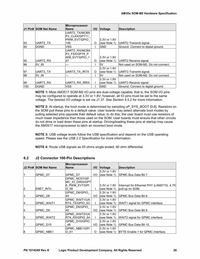
6.2 J2 Connector 100-Pin Descriptions
J2 Pin# SOM Net Name Microprocessor Name I/O Voltage Description
1 GPMC_D7 GPMC_D7 I/O 3.3V or 1.8V (see Note 1) GPMC Bus Data Bit 7.
2 ENET_INTn
GPMC_NCS7/GPMC_IO_DIR/0/GPT8_PWM_EVT/GPIO_58 I
3.3V or 1.8V (see Note 1)
Interrupt for Ethernet PHY (LAN9710). 4.7K pull-up on SOM.
3 GPMC_D8 GPMC_D8/GPIO_44 I/O
3.3V or 1.8V (see Note 1) GPMC Bus Data Bit 8.
4 GPMC_WAIT1 GPMC_WAIT1/UART4_TX/GPIO_63 I
3.3V or 1.8V (see Note 1) WAIT1 signal for GPMC interface.
5 GPMC_D9 GPMC_D9/GPIO_45 I/O
3.3V or 1.8V (see Note 1) GPMC Bus Data Bit 9.
6 GPMC_WAIT2 GPMC_WAIT2/UART4_RX/GPIO_64 I
3.3V or 1.8V (see Note 1) WAIT2 signal for GPMC interface.
7 GPMC_D10 GPMC_D10/GPIO_46 I/O
3.3V or 1.8V (see Note 1) GPMC Bus Data Bit 10.
8 GPMC_NBE1 GPMC_NBE1/GPIO_61 O
3.3V or 1.8V (see Note 1) BYTE Enable 1 for GPMC Interface.
AM35x SOM-M2 Hardware Specification
PN 1014249 Rev A Logic Product Development Company, All Rights Reserved 27
J2 Pin# SOM Net Name Microprocessor Name I/O Voltage Description
9 GPMC_D11 GPMC_D11/GPIO_47 I/O
3.3V or 1.8V (see Note 1) GPMC Bus Data Bit 11.
10 GPMC_NBE0_CLE GPMC_NBE0_CLE/GPIO_60 O
3.3V or 1.8V (see Note 1) BYTE Enable 0 for GPMC Interface.
11 GPMC_D12 GPMC_D11/GPIO_48 I/O
3.3V or 1.8V (see Note 1) GPMC Bus Data Bit 12.
12 GPMC_WEn GPMC_NWE O 3.3V or 1.8V (see Note 1) GPMC Bus Write Enable.
13 GPMC_D13 GPMC_D11/GPIO_49 I/O
3.3V or 1.8V (see Note 1) GPMC Bus Data Bit 13.
14 GPMC_OEn GPMC_NOE O 3.3V or 1.8V (see Note 1) GPMC Bus Output Enable.
15 GPMC_D14 GPMC_D11/GPIO_50 I/O
3.3V or 1.8V (see Note 1) GPMC Bus Data Bit 14.
16 GPMC_NADV_ALE GPMC_NADV_ALE O
3.3V or 1.8V (see Note 1) GPMC Bus Address Latch Enable.
17 GPMC_D15 GPMC_D11/GPIO_51 I/O
3.3V or 1.8V (see Note 1) GPMC Bus Data Bit 15.
18 GPMC_CLK GPMC_CLK/GPIO_59 O
3.3V or 1.8V (see Note 1) GPMC Bus Clock.
19 DGND VSS I GND Ground. Connect to digital ground. 20 DGND VSS I GND Ground. Connect to digital ground. 21 RFU — NA NA Reserved for future use. Do not connect.
22 GPMC_nCS5
GPMC_NCS5/SYS_NDMAREQ2/0/GPT10_PWM_EVT/GPIO_56 O
3.3V or 1.8V (see Note 1) GPMC Bus Chip Select 5.
23 GPMC_A1 GPMC_A1/GPIO_34 O
3.3V or 1.8V (see Note 1) GPMC Bus Address Bit 1.
24 RTCINTn
GPMC_NCS4/SYS_NDMAREQ1/GPT9_PWM_EVT/GPIO_55 O
3.3V or 1.8V (see Note 1)
Active low. Real Time Clock Interrupt. This signal has a 4.7k pull-up.
25 GPMC_A2 GPMC_A2/GPIO_35 O
3.3V or 1.8V (see Note 1) GPMC Bus Address Bit 2.
26 GPMC_nCS3
GPMC_NCS3/SYS_NDMAREQ0/GPT10_PWM_EVT/GPIO_54 O
3.3V or 1.8V (see Note 1) GPMC Bus Chip Select 3.
27 GPMC_A3 GPMC_A3/GPIO_36 O
3.3V or 1.8V (see Note 1) GPMC Bus Address Bit 3.
28 GPMC_nCS2
GPMC_NCS2/GPT9_PWM_EVT/GPIO_53 O
3.3V or 1.8V (see Note 1) GPMC Bus Chip Select 2.
29 GPMC_A4 GPMC_A4/GPIO_37 O
3.3V or 1.8V (see Note 1) GPMC Bus Address Bit 4.
30 GPMC_nCS1 GPMC_NCS1/GPIO_52 O
3.3V or 1.8V (see Note 1) GPMC Bus Chip Select 1.
31 GPMC_A5 GPMC_A5/GPIO_38 O
3.3V or 1.8V (see Note 1) GPMC Bus Address Bit 5.
32 GPMC_nCS0 GPMC_nCS0 O 3.3V or 1.8V (see Note 1) GPMC Bus Chip Select 0.
33 GPMC_A6 GPMC_A6/GPIO_39 O
3.3V or 1.8V (see Note 1) GPMC Bus Address Bit 6.
34 GPMC_D0 GPMC_D0 I/O 3.3V or 1.8V (see Note 1) GPMC Bus Data Bit 0.
35 GPMC_A7 GPMC_A7/GPIO_40 O
3.3V or 1.8V (see Note 1) GPMC Bus Address Bit 7.
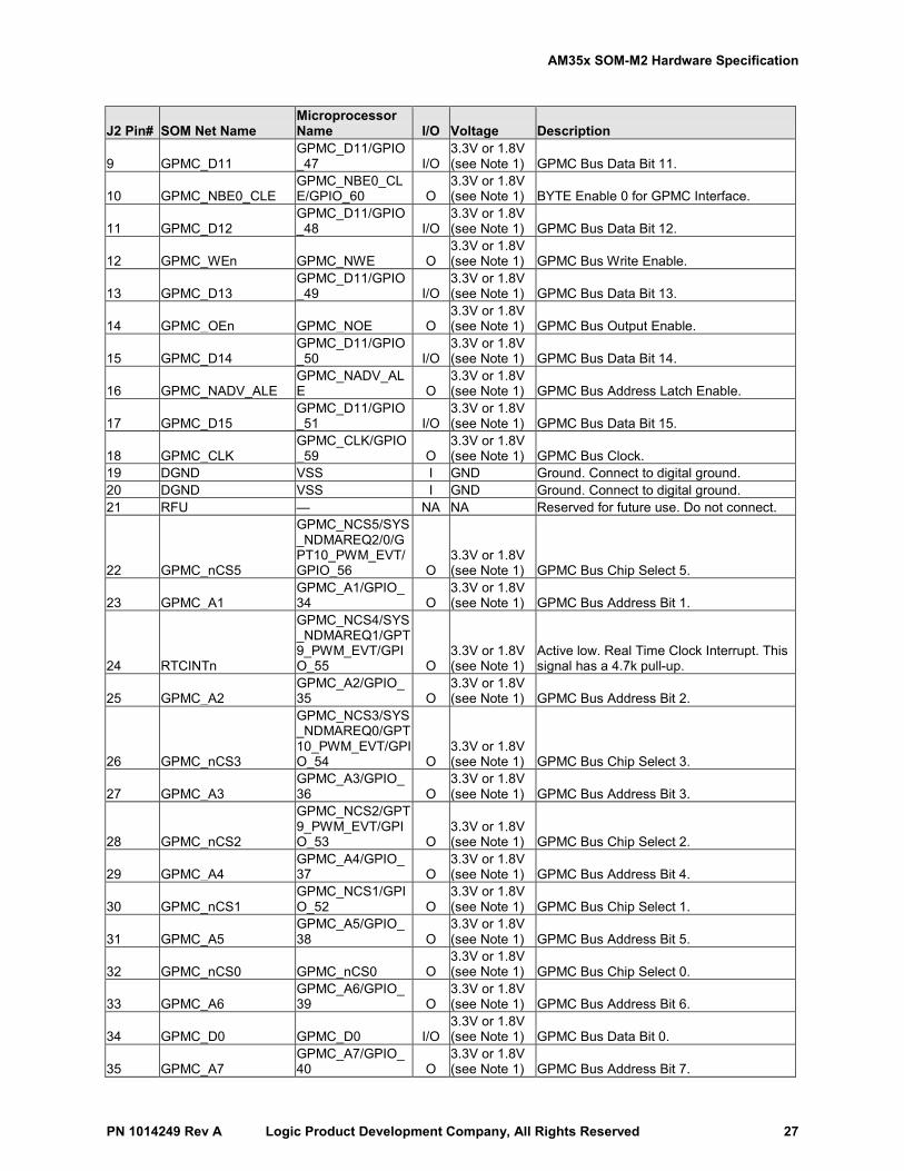
AM35x SOM-M2 Hardware Specification
PN 1014249 Rev A Logic Product Development Company, All Rights Reserved 28
J2 Pin# SOM Net Name Microprocessor Name I/O Voltage Description
36 GPMC_D1 GPMC_D1 I/O 3.3V or 1.8V (see Note 1) GPMC Bus Data Bit 1.
37 GPMC_A8 GPMC_A8/GPIO_41 O
3.3V or 1.8V (see Note 1) GPMC Bus Address Bit 8.
38 GPMC_D2 GPMC_D2 I/O 3.3V or 1.8V (see Note 1) GPMC Bus Data Bit 2.
39 GPMC_A9
GPMC_A9/SYS_NDMAREQ2/GPIO_42 O
3.3V or 1.8V (see Note 1) GPMC Bus Address Bit 9.
40 GPMC_D3 GPMC_D3 I/O 3.3V or 1.8V (see Note 1) GPMC Bus Data Bit 3.
41 GPMC_A10
GPMC_A10/SYS_NDMAREQ3/GPIO_43 O
3.3V or 1.8V (see Note 1) GPMC Bus Address Bit 10.
42 GPMC_D4 GPMC_D4 I/O 3.3V or 1.8V (see Note 1) GPMC Bus Data Bit 4.
43 RFU — NA NA Reserved for future use. Do not connect.
44 GPMC_D5 GPMC_D5 I/O 3.3V or 1.8V (see Note 1) GPMC Bus Data Bit 5.
45 RFU — NA NA Reserved for future use. Do not connect.
46 GPMC_D6 GPMC_D6 I/O 3.3V or 1.8V (see Note 1) GPMC Bus Data Bit 6.
47 DGND VSS I GND Ground. Connect to digital ground. 48 DGND VSS I GND Ground. Connect to digital ground.
49 MAIN_BATT_IN — I max 6V
External power source input. This signal should be driven directly by a single cell lithium-ion battery or a fixed regulated power source. See Sections 3.2 & 4.5.1.1.
50 MAIN_BATT_IN — I max 6V
External power source input. This signal should be driven directly by a single cell lithium-ion battery or a fixed regulated power source. See Sections 3.2 & 4.5.1.1.
51 MAIN_BATT_IN — I max 6V
External power source input. This signal should be driven directly by a single cell lithium-ion battery or a fixed regulated power source. See Sections 3.2 & 4.5.1.1..
52 MAIN_BATT_IN — I max 6V
External power source input. This signal should be driven directly by a single cell lithium-ion battery or a fixed regulated power source. See Sections 3.2 & 4.5.1.1.
53 DGND VSS I GND Ground. Connect to digital ground. 54 DGND VSS I GND Ground. Connect to digital ground. 55 RFU — NA NA Reserved for future use. Do not connect. 56 TV_OUT1 TV_OUT1 O — Composite/Luma S-Video (See Note 4).
57 ETHER_LINK_ACT_LEDn — O — Connect to anode of Ethernet Activity LED.
58 TV_OUT2 TV_OUT2 O Chroma S-Video (See Note 4).
59 uP_I2C3_SDA I2C3_SDA/GPIO_185 I/O
3.3V or 1.8V (see Note 1) I2C3 Serial Data.
60 uP_I2C2_SDA I2C2_SDA/GPIO_183 I/O
3.3V or 1.8V (see Note 1) I2C2 Serial Data.
61 uP_I2C3_SCL I2C3_SCL/GPIO_184 O
3.3V or 1.8V (see Note 1) I2C3 Serial Clock.
62 uP_I2C2_SCL I2C2_SDA/GPIO_168 O
3.3V or 1.8V (see Note 1) I2C2 Serial Clock.
63 ETHER_SPEED_LED — O — Connect to cathode of Ethernet Speed LED.
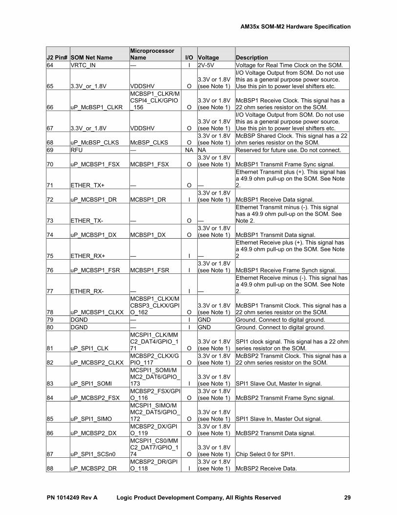
AM35x SOM-M2 Hardware Specification
PN 1014249 Rev A Logic Product Development Company, All Rights Reserved 29
J2 Pin# SOM Net Name Microprocessor Name I/O Voltage Description
64 VRTC_IN — I 2V-5V Voltage for Real Time Clock on the SOM.
65 3.3V_or_1.8V VDDSHV O 3.3V or 1.8V (see Note 1)
I/O Voltage Output from SOM. Do not use this as a general purpose power source. Use this pin to power level shifters etc.
66 uP_McBSP1_CLKR
MCBSP1_CLKR/MCSPI4_CLK/GPIO_156 O
3.3V or 1.8V (see Note 1)
McBSP1 Receive Clock. This signal has a 22 ohm series resistor on the SOM.
67 3.3V_or_1.8V VDDSHV O 3.3V or 1.8V (see Note 1)
I/O Voltage Output from SOM. Do not use this as a general purpose power source. Use this pin to power level shifters etc.
68 uP_McBSP_CLKS McBSP_CLKS O 3.3V or 1.8V (see Note 1)
McBSP Shared Clock. This signal has a 22 ohm series resistor on the SOM.
69 RFU — NA NA Reserved for future use. Do not connect.
70 uP_MCBSP1_FSX MCBSP1_FSX O 3.3V or 1.8V (see Note 1) McBSP1 Transmit Frame Sync signal.
71 ETHER_TX+ — O —
Ethernet Transmit plus (+). This signal has a 49.9 ohm pull-up on the SOM. See Note 2.
72 uP_MCBSP1_DR MCBSP1_DR I 3.3V or 1.8V (see Note 1) McBSP1 Receive Data signal.
73 ETHER_TX- — O —
Ethernet Transmit minus (-). This signal has a 49.9 ohm pull-up on the SOM. See Note 2.
74 uP_MCBSP1_DX MCBSP1_DX O 3.3V or 1.8V (see Note 1) McBSP1 Transmit Data signal.
75 ETHER_RX+ — I —
Ethernet Receive plus (+). This signal has a 49.9 ohm pull-up on the SOM. See Note 2
76 uP_MCBSP1_FSR MCBSP1_FSR I 3.3V or 1.8V (see Note 1) McBSP1 Receive Frame Synch signal.
77 ETHER_RX- — I —
Ethernet Receive minus (-). This signal has a 49.9 ohm pull-up on the SOM. See Note 2.
78 uP_MCBSP1_CLKX
MCBSP1_CLKX/MCBSP3_CLKX/GPIO_162 O
3.3V or 1.8V (see Note 1)
McBSP1 Transmit Clock. This signal has a 22 ohm series resistor on the SOM.
79 DGND — I GND Ground. Connect to digital ground. 80 DGND — I GND Ground. Connect to digital ground.
81 uP_SPI1_CLK
MCSPI1_CLK/MMC2_DAT4/GPIO_171 O
3.3V or 1.8V (see Note 1)
SPI1 clock signal. This signal has a 22 ohm series resistor on the SOM.
82 uP_MCBSP2_CLKX MCBSP2_CLKX/GPIO_117 O
3.3V or 1.8V (see Note 1)
McBSP2 Transmit Clock. This signal has a 22 ohm series resistor on the SOM.
83 uP_SPI1_SOMI
MCSPI1_SOMI/MMC2_DAT6/GPIO_173 I
3.3V or 1.8V (see Note 1) SPI1 Slave Out, Master In signal.
84 uP_MCBSP2_FSX MCBSP2_FSX/GPIO_116 O
3.3V or 1.8V (see Note 1) McBSP2 Transmit Frame Sync signal.
85 uP_SPI1_SIMO
MCSPI1_SIMO/MMC2_DAT5/GPIO_172 O
3.3V or 1.8V (see Note 1) SPI1 Slave In, Master Out signal.
86 uP_MCBSP2_DX MCBSP2_DX/GPIO_119 O
3.3V or 1.8V (see Note 1) McBSP2 Transmit Data signal.
87 uP_SPI1_SCSn0
MCSPI1_CS0/MMC2_DAT7/GPIO_174 O
3.3V or 1.8V (see Note 1) Chip Select 0 for SPI1.
88 uP_MCBSP2_DR MCBSP2_DR/GPIO_118 I
3.3V or 1.8V (see Note 1) McBSP2 Receive Data.
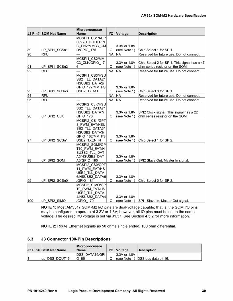
AM35x SOM-M2 Hardware Specification
PN 1014249 Rev A Logic Product Development Company, All Rights Reserved 30
J2 Pin# SOM Net Name Microprocessor Name I/O Voltage Description
89 uP_SPI1_SCSn1
MCSPI1_CS1/ADPLLV2D_DITHERING_EN2/MMC3_CMD/GPIO_175 O
3.3V or 1.8V (see Note 1) Chip Select 1 for SPI1.
90 RFU — NA NA Reserved for future use. Do not connect.
91 uP_SPI1_SCSn2
MCSPI1_CS2/MMC3_CLK/GPIO_176 O
3.3V or 1.8V (see Note 1)
Chip Select 2 for SPI1. This signal has a 47 ohm series resistor on the SOM.
92 RFU — NA NA Reserved for future use. Do not connect.
93 uP_SPI1_SCSn3
MCSPI1_CS3/HSUSB2_TLL_DATA2/HSUSB2_DATA2/GPIO_177/MM_FSUSB2_TXDAT O
3.3V or 1.8V (see Note 1) Chip Select 3 for SPI1.
94 RFU — NA NA Reserved for future use. Do not connect. 95 RFU — NA NA Reserved for future use. Do not connect.
96 uP_SPI2_CLK
MCSPI2_CLK/HSUSB2_TLL_DATA7/HSUSB2_DATA7/GPIO_178 O
3.3V or 1.8V (see Note 1)
SPI2 Clock signal. This signal has a 22 ohm series resistor on the SOM.
97 uP_SPI2_SCSn1
MCSPI2_CS1/GPT8_PWM_EVT/HSUSB2_TLL_DATA3/HSUSB2_DATA3/GPIO_182/MM_FSUSB2_TXEN_N O
3.3V or 1.8V (see Note 1) Chip Select 1 for SPI2.
98 uP_SPI2_SOMI
MCSPI2_SOMI/GPT10_PWM_EVT/HSUSB2_TLL_DATA5/HSUSB2_DATA5/GPIO_180 I
3.3V or 1.8V (see Note 1) SPI2 Slave Out, Master In signal.
99 uP_SPI2_SCSn0
MCSPI2_CS0/GPT11_PWM_EVT/HSUSB2_TLL_DATA6/HSUSB2_DATA6/GPIO_181 O
3.3V or 1.8V (see Note 1) Chip Select 0 for SPI2.
100 uP_SPI2_SIMO
MCSPI2_SIMO/GPT9_PWM_EVT/HSUSB2_TLL_DATA4/HSUSB2_DATA4/GPIO_179 O
3.3V or 1.8V (see Note 1) SPI1 Slave In, Master Out signal.
NOTE 1: Most AM3517 SOM-M2 I/O pins are dual-voltage capable; that is, the SOM I/O pins may be configured to operate at 3.3V or 1.8V; however, all IO pins must be set to the same voltage. The desired I/O voltage is set via J1.37. See Section 4.5.2 for more information.
NOTE 2: Route Ethernet signals as 50 ohms single ended, 100 ohm differential.
6.3 J3 Connector 100-Pin Descriptions
J3 Pin# SOM Net Name Microprocessor Name I/O Voltage Description
1 up_DSS_DOUT16 DSS_DATA16/GPIO_86 O
3.3V or 1.8V (see Note 1) DSS bus data bit 16.
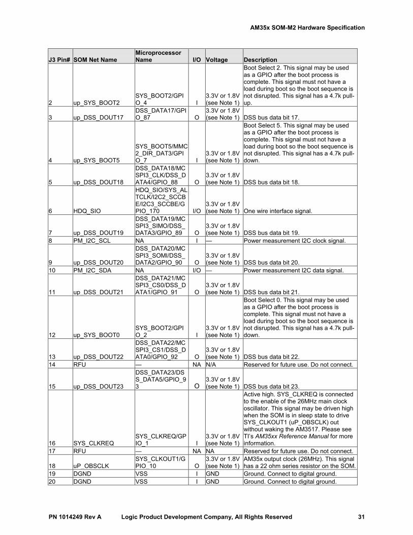
AM35x SOM-M2 Hardware Specification
PN 1014249 Rev A Logic Product Development Company, All Rights Reserved 31
J3 Pin# SOM Net Name Microprocessor Name I/O Voltage Description
2 up_SYS_BOOT2 SYS_BOOT2/GPIO_4 I
3.3V or 1.8V (see Note 1)
Boot Select 2. This signal may be used as a GPIO after the boot process is complete. This signal must not have a load during boot so the boot sequence is not disrupted. This signal has a 4.7k pull-up.
3 up_DSS_DOUT17 DSS_DATA17/GPIO_87 O
3.3V or 1.8V (see Note 1) DSS bus data bit 17.
4 up_SYS_BOOT5
SYS_BOOT5/MMC2_DIR_DAT3/GPIO_7 I
3.3V or 1.8V (see Note 1)
Boot Select 5. This signal may be used as a GPIO after the boot process is complete. This signal must not have a load during boot so the boot sequence is not disrupted. This signal has a 4.7k pull-down.
5 up_DSS_DOUT18
DSS_DATA18/MCSPI3_CLK/DSS_DATA4/GPIO_88 O
3.3V or 1.8V (see Note 1) DSS bus data bit 18.
6 HDQ_SIO
HDQ_SIO/SYS_ALTCLK/I2C2_SCCBE/I2C3_SCCBE/GPIO_170 I/O
3.3V or 1.8V (see Note 1) One wire interface signal.
7 up_DSS_DOUT19
DSS_DATA19/MCSPI3_SIMO/DSS_DATA3/GPIO_89 O
3.3V or 1.8V (see Note 1) DSS bus data bit 19.
8 PM_I2C_SCL NA I — Power measurement I2C clock signal.
9 up_DSS_DOUT20
DSS_DATA20/MCSPI3_SOMI/DSS_DATA2/GPIO_90 O
3.3V or 1.8V (see Note 1) DSS bus data bit 20.
10 PM_I2C_SDA NA I/O — Power measurement I2C data signal.
11 up_DSS_DOUT21
DSS_DATA21/MCSPI3_CS0/DSS_DATA1/GPIO_91 O
3.3V or 1.8V (see Note 1) DSS bus data bit 21.
12 up_SYS_BOOT0 SYS_BOOT2/GPIO_2 I
3.3V or 1.8V (see Note 1)
Boot Select 0. This signal may be used as a GPIO after the boot process is complete. This signal must not have a load during boot so the boot sequence is not disrupted. This signal has a 4.7k pull-down.
13 up_DSS_DOUT22
DSS_DATA22/MCSPI3_CS1/DSS_DATA0/GPIO_92 O
3.3V or 1.8V (see Note 1) DSS bus data bit 22.
14 RFU — NA N/A Reserved for future use. Do not connect.
15 up_DSS_DOUT23
DSS_DATA23/DSS_DATA5/GPIO_93 O
3.3V or 1.8V (see Note 1) DSS bus data bit 23.
16 SYS_CLKREQ SYS_CLKREQ/GPIO_1 I
3.3V or 1.8V (see Note 1)
Active high. SYS_CLKREQ is connected to the enable of the 26MHz main clock oscillator. This signal may be driven high when the SOM is in sleep state to drive SYS_CLKOUT1 (uP_OBSCLK) out without waking the AM3517. Please see TI’s AM35xx Reference Manual for more information.
17 RFU — NA NA Reserved for future use. Do not connect.
18 uP_OBSCLK SYS_CLKOUT1/GPIO_10 O
3.3V or 1.8V (see Note 1)
AM35x output clock (26MHz). This signal has a 22 ohm series resistor on the SOM.
19 DGND VSS I GND Ground. Connect to digital ground. 20 DGND VSS I GND Ground. Connect to digital ground.
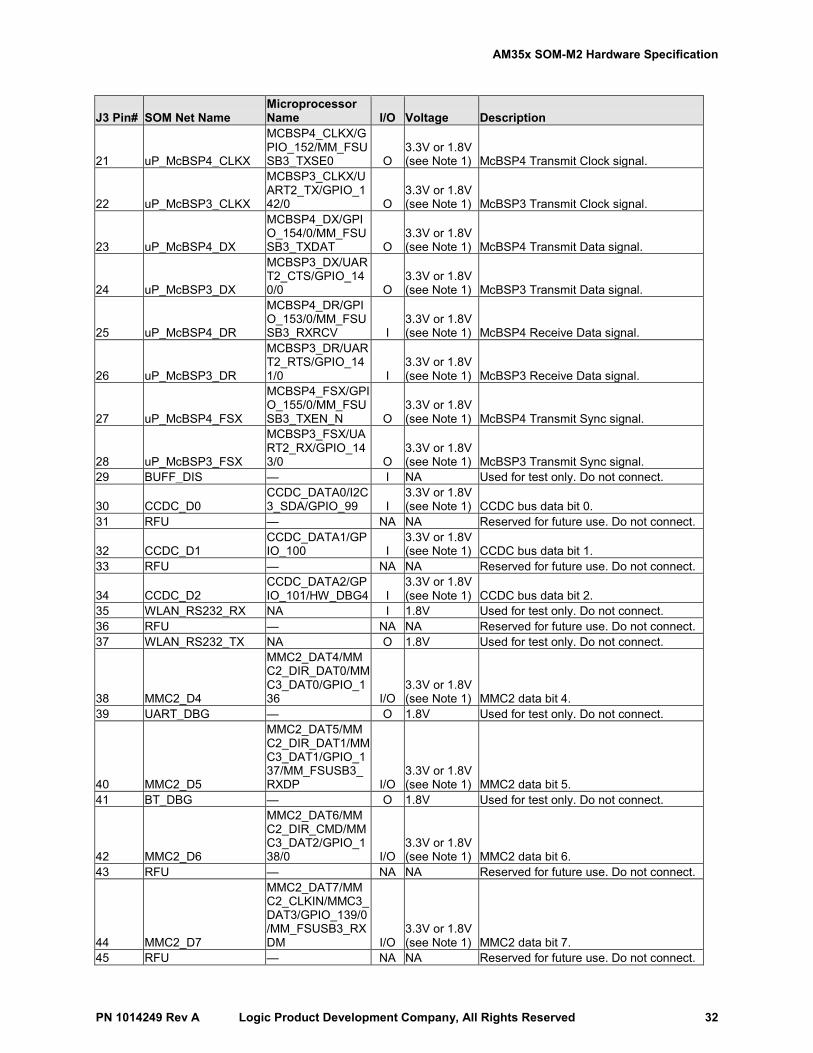
AM35x SOM-M2 Hardware Specification
PN 1014249 Rev A Logic Product Development Company, All Rights Reserved 32
J3 Pin# SOM Net Name Microprocessor Name I/O Voltage Description
21 uP_McBSP4_CLKX
MCBSP4_CLKX/GPIO_152/MM_FSUSB3_TXSE0 O
3.3V or 1.8V (see Note 1) McBSP4 Transmit Clock signal.
22 uP_McBSP3_CLKX
MCBSP3_CLKX/UART2_TX/GPIO_142/0 O
3.3V or 1.8V (see Note 1) McBSP3 Transmit Clock signal.
23 uP_McBSP4_DX
MCBSP4_DX/GPIO_154/0/MM_FSUSB3_TXDAT O
3.3V or 1.8V (see Note 1) McBSP4 Transmit Data signal.
24 uP_McBSP3_DX
MCBSP3_DX/UART2_CTS/GPIO_140/0 O
3.3V or 1.8V (see Note 1) McBSP3 Transmit Data signal.
25 uP_McBSP4_DR
MCBSP4_DR/GPIO_153/0/MM_FSUSB3_RXRCV I
3.3V or 1.8V (see Note 1) McBSP4 Receive Data signal.
26 uP_McBSP3_DR
MCBSP3_DR/UART2_RTS/GPIO_141/0 I
3.3V or 1.8V (see Note 1) McBSP3 Receive Data signal.
27 uP_McBSP4_FSX
MCBSP4_FSX/GPIO_155/0/MM_FSUSB3_TXEN_N O
3.3V or 1.8V (see Note 1) McBSP4 Transmit Sync signal.
28 uP_McBSP3_FSX
MCBSP3_FSX/UART2_RX/GPIO_143/0 O
3.3V or 1.8V (see Note 1) McBSP3 Transmit Sync signal.
29 BUFF_DIS — I NA Used for test only. Do not connect.
30 CCDC_D0 CCDC_DATA0/I2C3_SDA/GPIO_99 I
3.3V or 1.8V (see Note 1) CCDC bus data bit 0.
31 RFU — NA NA Reserved for future use. Do not connect.
32 CCDC_D1 CCDC_DATA1/GPIO_100 I
3.3V or 1.8V (see Note 1) CCDC bus data bit 1.
33 RFU — NA NA Reserved for future use. Do not connect.
34 CCDC_D2 CCDC_DATA2/GPIO_101/HW_DBG4 I
3.3V or 1.8V (see Note 1) CCDC bus data bit 2.
35 WLAN_RS232_RX NA I 1.8V Used for test only. Do not connect. 36 RFU — NA NA Reserved for future use. Do not connect. 37 WLAN_RS232_TX NA O 1.8V Used for test only. Do not connect.
38 MMC2_D4
MMC2_DAT4/MMC2_DIR_DAT0/MMC3_DAT0/GPIO_136 I/O
3.3V or 1.8V (see Note 1) MMC2 data bit 4.
39 UART_DBG — O 1.8V Used for test only. Do not connect.
40 MMC2_D5
MMC2_DAT5/MMC2_DIR_DAT1/MMC3_DAT1/GPIO_137/MM_FSUSB3_RXDP I/O
3.3V or 1.8V (see Note 1) MMC2 data bit 5.
41 BT_DBG — O 1.8V Used for test only. Do not connect.
42 MMC2_D6
MMC2_DAT6/MMC2_DIR_CMD/MMC3_DAT2/GPIO_138/0 I/O
3.3V or 1.8V (see Note 1) MMC2 data bit 6.
43 RFU — NA NA Reserved for future use. Do not connect.
44 MMC2_D7
MMC2_DAT7/MMC2_CLKIN/MMC3_DAT3/GPIO_139/0/MM_FSUSB3_RXDM I/O
3.3V or 1.8V (see Note 1) MMC2 data bit 7.
45 RFU — NA NA Reserved for future use. Do not connect.
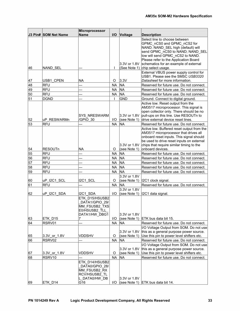
AM35x SOM-M2 Hardware Specification
PN 1014249 Rev A Logic Product Development Company, All Rights Reserved 33
J3 Pin# SOM Net Name Microprocessor Name I/O Voltage Description
46 NAND_SEL — I 3.3V or 1.8V (See Note 1)
Select line to choose between GPMC_nCS0 and GPMC_nCS2 for NAND. NAND_SEL high (default) will send GPMC_nCS0 to NAND; NAND_SEL low will send GPMC_nCS2 to NAND. Please refer to the Application Board schematics for an example of external chip select usage.
47 USB1_CPEN NA O 3.3V
External VBUS power supply control for USB1. Please see the SMSC USB3320 Datasheet for more information.
48 RFU — NA NA Reserved for future use. Do not connect. 49 RFU — NA NA Reserved for future use. Do not connect. 50 RFU — NA NA Reserved for future use. Do not connect. 51 DGND — I GND Ground. Connect to digital ground.
52 uP_RESWARMn SYS_NRESWARM/GPIO_30 I/O
3.3V or 1.8V (see Note 1)
Active low. Reset output from the AM3517 microprocessor. This signal is open collector only. There should be no pull-ups on this line. Use RESOUTn to drive external device reset lines.
53 RFU — NA NA Reserved for future use. Do not connect.
54 RESOUTn NA O 3.3V or 1.8V (see Note 1)
Active low. Buffered reset output from the AM3517 microprocessor that drives all onboard reset inputs. This signal should be used to drive reset inputs on external chips that require similar timing to the onboard devices.
55 RFU — NA NA Reserved for future use. Do not connect. 56 RFU — NA NA Reserved for future use. Do not connect. 57 RFU — NA NA Reserved for future use. Do not connect. 58 RFU — NA NA Reserved for future use. Do not connect. 59 RFU — NA NA Reserved for future use. Do not connect.
60 uP_I2C1_SCL I2C1_SCL O 3.3V or 1.8V (see Note 1) I2C1 clock signal.
61 RFU — NA NA Reserved for future use. Do not connect.
62 uP_I2C1_SDA I2C1_SDA I/O 3.3V or 1.8V (see Note 1) I2C1 data signal.
63 ETK_D15
ETK_D15/HSUSB2_DATA1/GPIO_29/MM_FSUSB2_TXSE0/HSUSB2_TLL_DATA1/HW_DBG17 I/O
3.3V or 1.8V (see Note 1) ETK bus data bit 15.
64 RSRV01 — NA NA Reserved for future use. Do not connect.
65 3.3V_or_1.8V VDDSHV O 3.3V or 1.8V (see Note 1)
I/O Voltage Output from SOM. Do not use this as a general purpose power source. Use this pin to power level shifters etc.
66 RSRV02 — NA NA Reserved for future use. Do not connect.
67 3.3V_or_1.8V VDDSHV O 3.3V or 1.8V (see Note 1)
I/O Voltage Output from SOM. Do not use this as a general purpose power source. Use this pin to power level shifters etc.
68 RSRV10 — NA NA Reserved for future use. Do not connect.
69 ETK_D14
ETK_D14/HSUSB2_DATA0/GPIO_28/MM_FSUSB2_RXRCV/HSUSB2_TLL_DATA0/HW_DBG16 I/O
3.3V or 1.8V (see Note 1) ETK bus data bit 14.
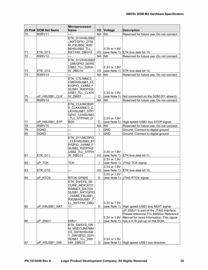
AM35x SOM-M2 Hardware Specification
PN 1014249 Rev A Logic Product Development Company, All Rights Reserved 34
J3 Pin# SOM Net Name Microprocessor Name I/O Voltage Description
70 RSRV11 — NA NA Reserved for future use. Do not connect.
71 ETK_D13
ETK_D13/HSUSB2_NXT/GPIO_27/MM_FSUSB2_RXDM/HSUSB2_TLL_NXT/HW_DBG15 I/O
3.3V or 1.8V (see Note 1) ETK bus data bit 13.
72 RSRV12 — NA NA Reserved for future use. Do not connect.
73 ETK_D12
ETK_D12/HSUSB2_DIR/GPIO_26/HSUSB2_TLL_DIR/HW_DBG14 I/O
3.3V or 1.8V (see Note 1) ETK bus data bit 12.
74 RSRV13 — NA NA Reserved for future use. Do not connect.
75 uP_HSUSB1_CLK
ETK_CTL/MMC3_CMD/HSUSB1_CLK/GPIO_13/MM_FSUSB1_RXDP/HSUSB1_TLL_CLK/HW_DBG1 O
3.3V or 1.8V (see Note 1) Not connected on the SOM (R1 absent).
76 RSRV14 — NA NA Reserved for future use. Do not connect.
77 uP_HSUSB1_STP
ETK_CLK/MCBSP5_CLKX/MMC3_CLK/HSUSB1_STP/GPIO_12/HSUSB1_TLL_STP/HW_DBG0 O
3.3V or 1.8V (see Note 1) High speed USB1 bus STOP signal.
78 RSRV15 — NA NA Reserved for future use. Do not connect. 79 DGND — I GND Ground. Connect to digital ground. 80 DGND — I GND Ground. Connect to digital ground.
81 ETK_D11
ETK_D11/MCSPI3_CLK/HSUSB2_STP/GPIO_25/MM_FSUSB2_RXDP/HSUSB2_TLL_STP/HW_DBG13 I/O
3.3V or 1.8V (see Note 1) ETK bus data bit 11.
82 uP_TCK TCK I 3.3V or 1.8V (see Note 1) JTAG TCK signal.
83 ETK_D10 — I/O 3.3V or 1.8V (see Note 1) ETK bus data bit 10.
84 uP_RTCK RTCK/ GP8[0] O 3.3V or 1.8V (see Note 1) JTAG RTCK signal.
85 uP_HSUSB1_NXT
ETK_D9/SYS_SECURE_INDICATOR/MMC3_DAT5/HSUSB1_NXT/GPIO_23/MM_FSUSB1_RXDM/HSUSB1_TLL_NXT/HW_DBG11 O
3.3V or 1.8V (see Note 1) High speed USB1 bus NEXT signal.
86 uP_EMU1 EMU1 I 3.3V or 1.8V (see Note 1)
uP_EMU1 is part of the JTAG interface. Please reference TI’s AM35xx Reference Manual for more information. This signal has a 4.7k pull-up on the SOM.
87 uP_HSUSB1_DIR
ETK_D8/SYS_DRM_MSECURE/MMC3_DAT6/HSUSB1_DIR/GPIO_22/HSUSB1_TLL_DIR/HW_DBG10 O
3.3V or 1.8V (see Note 1) High speed USB1 bus direction.
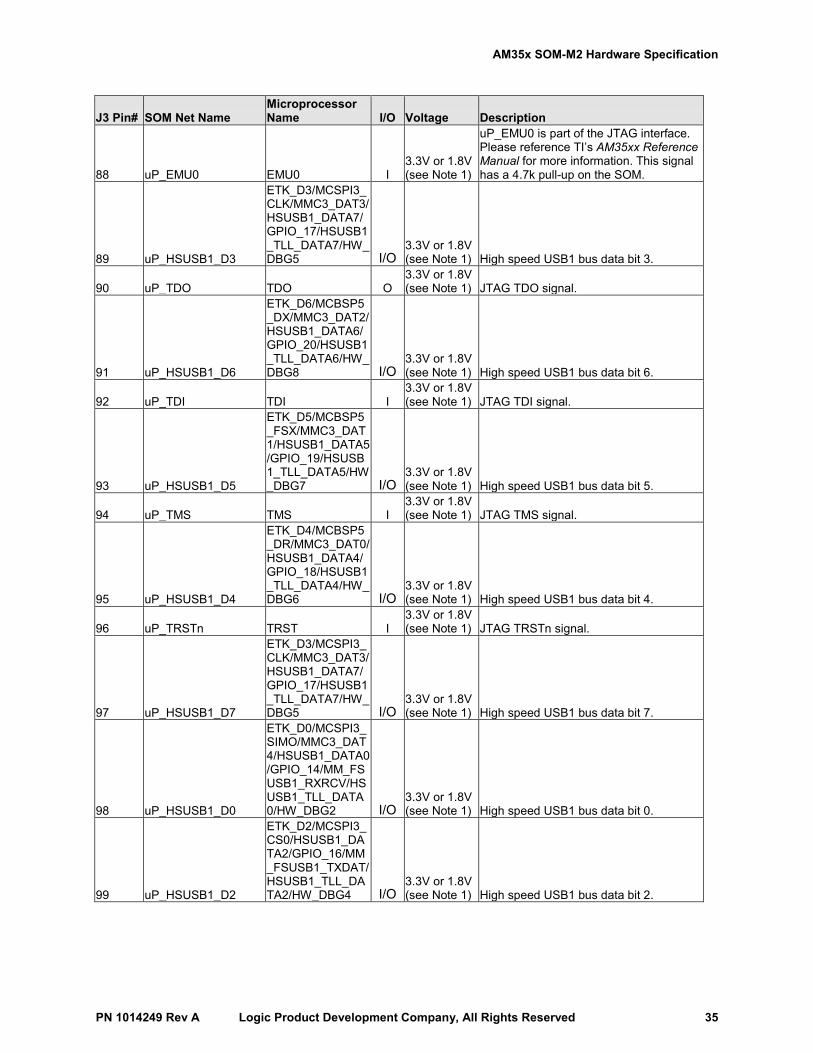
AM35x SOM-M2 Hardware Specification
PN 1014249 Rev A Logic Product Development Company, All Rights Reserved 35
J3 Pin# SOM Net Name Microprocessor Name I/O Voltage Description
88 uP_EMU0 EMU0 I 3.3V or 1.8V (see Note 1)
uP_EMU0 is part of the JTAG interface. Please reference TI’s AM35xx Reference Manual for more information. This signal has a 4.7k pull-up on the SOM.
89 uP_HSUSB1_D3
ETK_D3/MCSPI3_CLK/MMC3_DAT3/HSUSB1_DATA7/GPIO_17/HSUSB1_TLL_DATA7/HW_DBG5 I/O
3.3V or 1.8V (see Note 1) High speed USB1 bus data bit 3.
90 uP_TDO TDO O 3.3V or 1.8V (see Note 1) JTAG TDO signal.
91 uP_HSUSB1_D6
ETK_D6/MCBSP5_DX/MMC3_DAT2/HSUSB1_DATA6/GPIO_20/HSUSB1_TLL_DATA6/HW_DBG8 I/O
3.3V or 1.8V (see Note 1) High speed USB1 bus data bit 6.
92 uP_TDI TDI I 3.3V or 1.8V (see Note 1) JTAG TDI signal.
93 uP_HSUSB1_D5
ETK_D5/MCBSP5_FSX/MMC3_DAT1/HSUSB1_DATA5/GPIO_19/HSUSB1_TLL_DATA5/HW_DBG7 I/O
3.3V or 1.8V (see Note 1) High speed USB1 bus data bit 5.
94 uP_TMS TMS I 3.3V or 1.8V (see Note 1) JTAG TMS signal.
95 uP_HSUSB1_D4
ETK_D4/MCBSP5_DR/MMC3_DAT0/HSUSB1_DATA4/GPIO_18/HSUSB1_TLL_DATA4/HW_DBG6 I/O
3.3V or 1.8V (see Note 1) High speed USB1 bus data bit 4.
96 uP_TRSTn TRST I 3.3V or 1.8V (see Note 1) JTAG TRSTn signal.
97 uP_HSUSB1_D7
ETK_D3/MCSPI3_CLK/MMC3_DAT3/HSUSB1_DATA7/GPIO_17/HSUSB1_TLL_DATA7/HW_DBG5 I/O
3.3V or 1.8V (see Note 1) High speed USB1 bus data bit 7.
98 uP_HSUSB1_D0
ETK_D0/MCSPI3_SIMO/MMC3_DAT4/HSUSB1_DATA0/GPIO_14/MM_FSUSB1_RXRCV/HSUSB1_TLL_DATA0/HW_DBG2 I/O
3.3V or 1.8V (see Note 1) High speed USB1 bus data bit 0.
99 uP_HSUSB1_D2
ETK_D2/MCSPI3_CS0/HSUSB1_DATA2/GPIO_16/MM_FSUSB1_TXDAT/HSUSB1_TLL_DATA2/HW_DBG4 I/O
3.3V or 1.8V (see Note 1) High speed USB1 bus data bit 2.
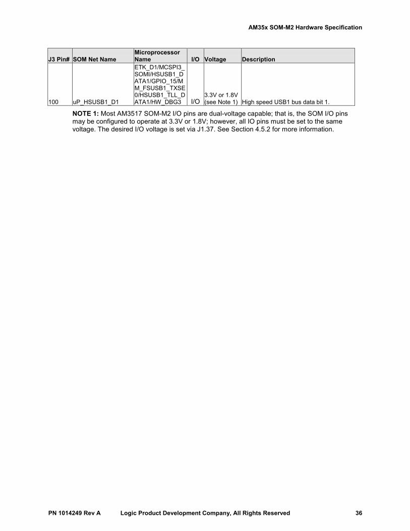
AM35x SOM-M2 Hardware Specification
PN 1014249 Rev A Logic Product Development Company, All Rights Reserved 36
J3 Pin# SOM Net Name Microprocessor Name I/O Voltage Description
100 uP_HSUSB1_D1
ETK_D1/MCSPI3_SOMI/HSUSB1_DATA1/GPIO_15/MM_FSUSB1_TXSE0/HSUSB1_TLL_DATA1/HW_DBG3 I/O
3.3V or 1.8V (see Note 1) High speed USB1 bus data bit 1.
NOTE 1: Most AM3517 SOM-M2 I/O pins are dual-voltage capable; that is, the SOM I/O pins may be configured to operate at 3.3V or 1.8V; however, all IO pins must be set to the same voltage. The desired I/O voltage is set via J1.37. See Section 4.5.2 for more information.
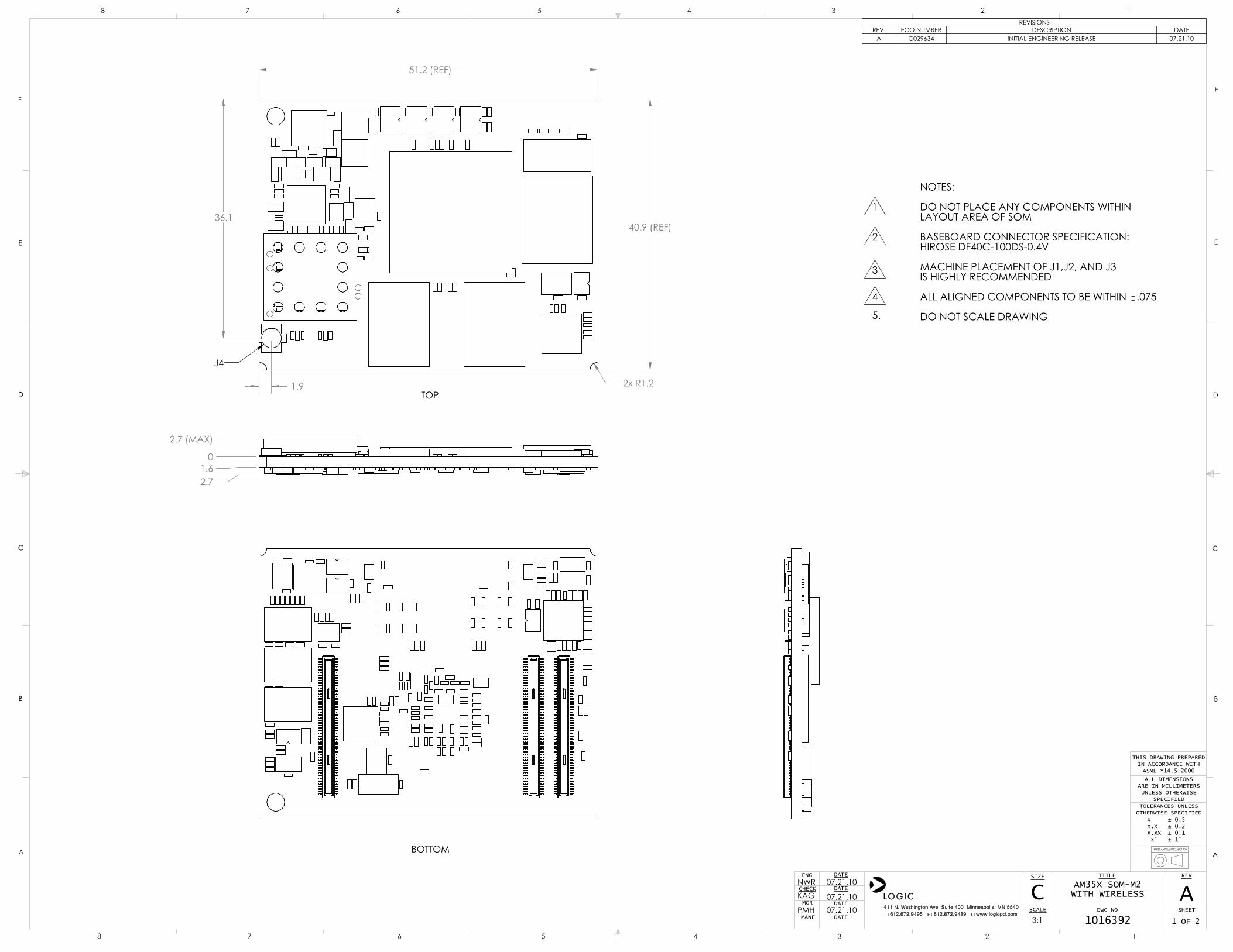
THIRD ANGLE PROJECTION
51.2 (REF)
40.9 (REF)36.1
1.9 2x R1.2TOP
J4
0
2.7 (MAX)
2.71.6
BOTTOM
4
3
5.
2
1
NOTES:
DO NOT PLACE ANY COMPONENTS WITHINLAYOUT AREA OF SOM
BASEBOARD CONNECTOR SPECIFICATION:HIROSE DF40C-100DS-0.4V
MACHINE PLACEMENT OF J1,J2, AND J3IS HIGHLY RECOMMENDED
ALL ALIGNED COMPONENTS TO BE WITHIN .075
DO NOT SCALE DRAWING
REVISIONSREV. ECO NUMBER DESCRIPTION DATE
A C029634 INITIAL ENGINEERING RELEASE 07.21.10
D
C
B
A
B
C
D
12345678
8 7 6 5 4 3 2 1
E
F
E
F
A
DATE
MANF
TITLE
DWG NO
REV
SHEETSCALE
SIZE
3:1 1 OF 2
ENG
CHECK DATE
DATE
C A1016392
AM35X SOM-M2WITH WIRELESS
TOLERANCES UNLESSOTHERWISE SPECIFIED
X ± 0.5X.X ± 0.2X.XX ± 0.1 X° ± 1°
ALL DIMENSIONSARE IN MILLIMETERSUNLESS OTHERWISE
SPECIFIED
THIS DRAWING PREPAREDIN ACCORDANCE WITHASME Y14.5-2000
DATEMGR
NWR 07.21.10
KAG 07.21.1007.21.10PMH
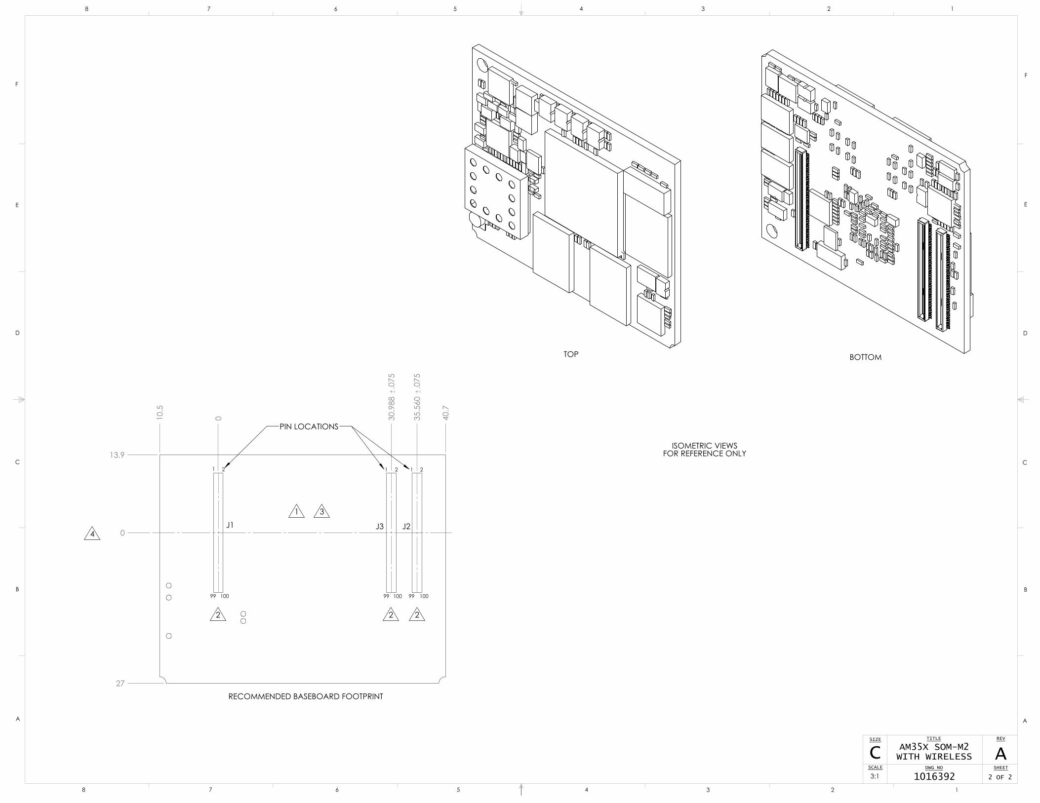
TOP BOTTOM
010.5
30.9
88
.075
40.7
35.5
60
.075
0
13.9
27RECOMMENDED BASEBOARD FOOTPRINT
J1 J3 J2
2
99 100
1 2
99 100 99
1 2
100
4
ISOMETRIC VIEWSFOR REFERENCE ONLY
1
PIN LOCATIONS
1 3
2 2 2
D
C
B
A
B
C
D
12345678
8 7 6 5 4 3 2 1
E
F
E
F
A
TITLE
DWG NO
REV
SHEETSCALE
SIZE
3:1 2 OF 2
C A1016392
AM35X SOM-M2WITH WIRELESS
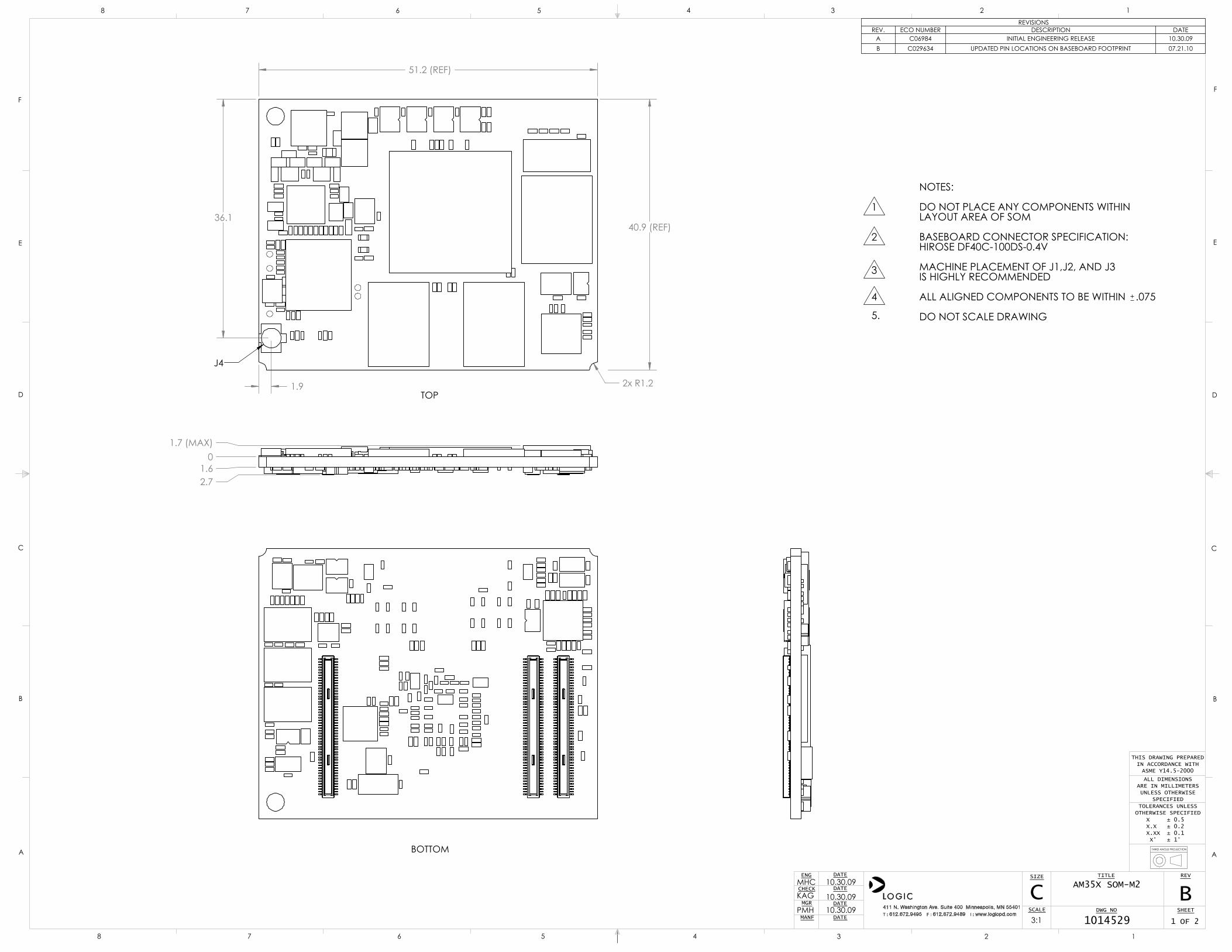
THIRD ANGLE PROJECTION
51.2 (REF)
40.9 (REF)36.1
1.9 2x R1.2TOP
J4
01.7 (MAX)
2.71.6
BOTTOM
4
3
5.
2
1
NOTES:
DO NOT PLACE ANY COMPONENTS WITHINLAYOUT AREA OF SOM
BASEBOARD CONNECTOR SPECIFICATION:HIROSE DF40C-100DS-0.4V
MACHINE PLACEMENT OF J1,J2, AND J3IS HIGHLY RECOMMENDED
ALL ALIGNED COMPONENTS TO BE WITHIN .075
DO NOT SCALE DRAWING
REVISIONSREV. ECO NUMBER DESCRIPTION DATE
A C06984 INITIAL ENGINEERING RELEASE 10.30.09B C029634 UPDATED PIN LOCATIONS ON BASEBOARD FOOTPRINT 07.21.10
D
C
B
A
B
C
D
12345678
8 7 6 5 4 3 2 1
E
F
E
F
A
DATE
MANF
TITLE
DWG NO
REV
SHEETSCALE
SIZE
3:1 1 OF 2
ENG
CHECK DATE
DATE
C B1014529
AM35X SOM-M2
TOLERANCES UNLESSOTHERWISE SPECIFIED
X ± 0.5X.X ± 0.2X.XX ± 0.1 X° ± 1°
ALL DIMENSIONSARE IN MILLIMETERSUNLESS OTHERWISE
SPECIFIED
THIS DRAWING PREPAREDIN ACCORDANCE WITHASME Y14.5-2000
DATEMGR
MHC 10.30.09
KAG 10.30.0910.30.09PMH

TOP BOTTOM
010.5
30.9
88
.075
40.7
35.5
60
.075
0
13.9
27RECOMMENDED BASEBOARD FOOTPRINT
J1 J3 J2
2
99 100
1 2
99 100 99
1 2
100
4
ISOMETRIC VIEWSFOR REFERENCE ONLY
1
PIN LOCATIONS
1 3
2 2 2
D
C
B
A
B
C
D
12345678
8 7 6 5 4 3 2 1
E
F
E
F
A
TITLE
DWG NO
REV
SHEETSCALE
SIZE
3:1 2 OF 2
C B1014529
AM35X SOM-M2
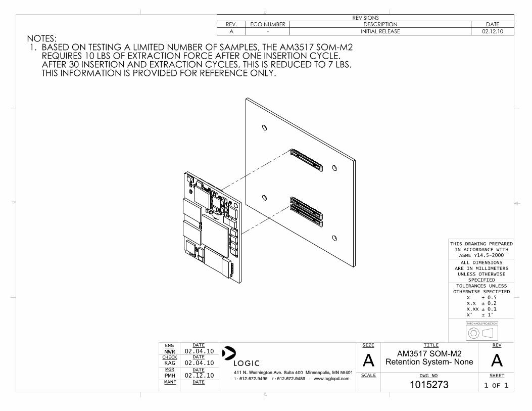
THIRD ANGLE PROJECTION
NOTES: 1. BASED ON TESTING A LIMITED NUMBER OF SAMPLES, THE AM3517 SOM-M2 REQUIRES 10 LBS OF EXTRACTION FORCE AFTER ONE INSERTION CYCLE. AFTER 30 INSERTION AND EXTRACTION CYCLES, THIS IS REDUCED TO 7 LBS. THIS INFORMATION IS PROVIDED FOR REFERENCE ONLY.
REVISIONSREV. ECO NUMBER DESCRIPTION DATE
A - INITIAL RELEASE 02.12.10
MGR DATE
THIS DRAWING PREPAREDIN ACCORDANCE WITHASME Y14.5-2000
ALL DIMENSIONSARE IN MILLIMETERSUNLESS OTHERWISE
SPECIFIED
X ± 0.5X.X ± 0.2X.XX ± 0.1X° ± 1°
TOLERANCES UNLESSOTHERWISE SPECIFIED
AM3517 SOM-M2 Retention System- None
1015273
AA02.04.10
02.04.10NWRDATE
DATECHECK
ENG
1 OF 1
SIZE
SCALE SHEET
REV
DWG NO
TITLE
MANF02.12.10
DATE
KAG
PMH
THIRD ANGLE PROJECTION
NOTES:1. THIS IS AN EXAMPLE RETENTION METHOD USING A CLIP.
REVISIONSREV. ECO NUMBER DESCRIPTION DATE
A - INITIAL RELEASE 02.12.10
MGR DATE
THIS DRAWING PREPAREDIN ACCORDANCE WITHASME Y14.5-2000
ALL DIMENSIONSARE IN MILLIMETERS
SPECIFIED
X ± 0.5X.X ± 0.2X.XX ± 0.1X° ± 1°
TOLERANCES UNLESSOTHERWISE SPECIFIED
AM3517 SOM-M2 Retention System - Clip
1015274
AA02.04.10
02.04.10NWRDATE
DATECHECK
ENG
1 OF 1
SIZE
SCALE SHEET
REV
DWG NO
TITLE
MANF02.12.10
DATE
KAG
PMH
THIRD ANGLE PROJECTION
2
NOTES:1. THE AM3517 SOM-M2 CAN BE RETAINED IN PLACE BY THE SURROUNDING ENCLOSURE.
2. REPRESENTATIVE ENCLOSURE
REVISIONSREV. ECO NUMBER DESCRIPTION DATE
A - INITIAL RELEASE 02.12.10
MGR DATE
THIS DRAWING PREPAREDIN ACCORDANCE WITHASME Y14.5-2000
ALL DIMENSIONSARE IN MILLIMETERSUNLESS OTHERWISE
SPECIFIED
X ± 0.5X.X ± 0.2X.XX ± 0.1X° ± 1°
TOLERANCES UNLESSOTHERWISE SPECIFIED
AM3517 SOM-M2 Retention System - Housing
1015275
AA02.04.10
02.04.10NWRDATE
DATECHECK
ENG
1 OF 1
SIZE
SCALE SHEET
REV
DWG NO
TITLE
MANF02.12.10
DATE
KAG
PMH