Embed Size (px)
Citation preview

Alan Kost
Frontiers in OpticsTucson, AZ
October 20, 2005
Monolithically Integrated Semiconductor Components for Coarse Wavelength
Division Multiplexing

OUTLINE
• The need for photonic integrated circuits
• Coarse wavelength division multiplexing- Arrayed waveguide gratings on InP
• Quantum Well Intermixing- GaAsSb Quantum Wells
Low cost is the driver

ELECTRONIC ICs

A WDM Data Link
LASEROPTICAL
MODULATOR
MULTIPLEXER DE-MULTIPLEXER
1
2
n
1, … n ADD
FIBER
POWERAMP DROP
i
j
PRE-AMP
IN-LINEAMP
1
2
m
VARIABLEATTENUATOR
PHOTODIODE
Components are numerous and expensive
OURPROGRAM

AWG/SOA Concept
1 cm
ArrayedWaveguide
Grating (AWG)
1 to 9Coupler
9 to 4Coupler
4Semiconductor
Optical Amplifiers(SOAs)
4
InP Substrate
= 20nm
De-multiplexing, amplification, and equalization on one, InP chip
1 cm

Coarse Wavelength Division Multiplexing
DWDM
• Very high throughput (80 channels over C-Band from 1530 to 1565 nm)
• For use in long haul networks
• Stabilized lasers and narrow-band filters required
32 nm
50 GHz (~0.4 nm at 1.55 m)
CWDM
• Smaller number of channels and correspondingly smaller throughput• For use in short to medium haul networks
• Compatible with less expensive, un-stabilized lasers and broadband filters
340 nm (1270 – 1610 nm)
= 20 nm

InP
ARRAYED WAVEGUIDE GRATINGS:“HORSESHOE” TYPE
SYMMETRY LINE
Tra
nsm
issi
on
1 2 3 4 1 2 3 4
OutputWaveguide #
Free Spectral Range OPTICAL PATHLENGTH = L
L + L
L + 2L
L + 3LL + 4L
L + 5L
L = m
1
Small for CWDM
FSRL
L
~
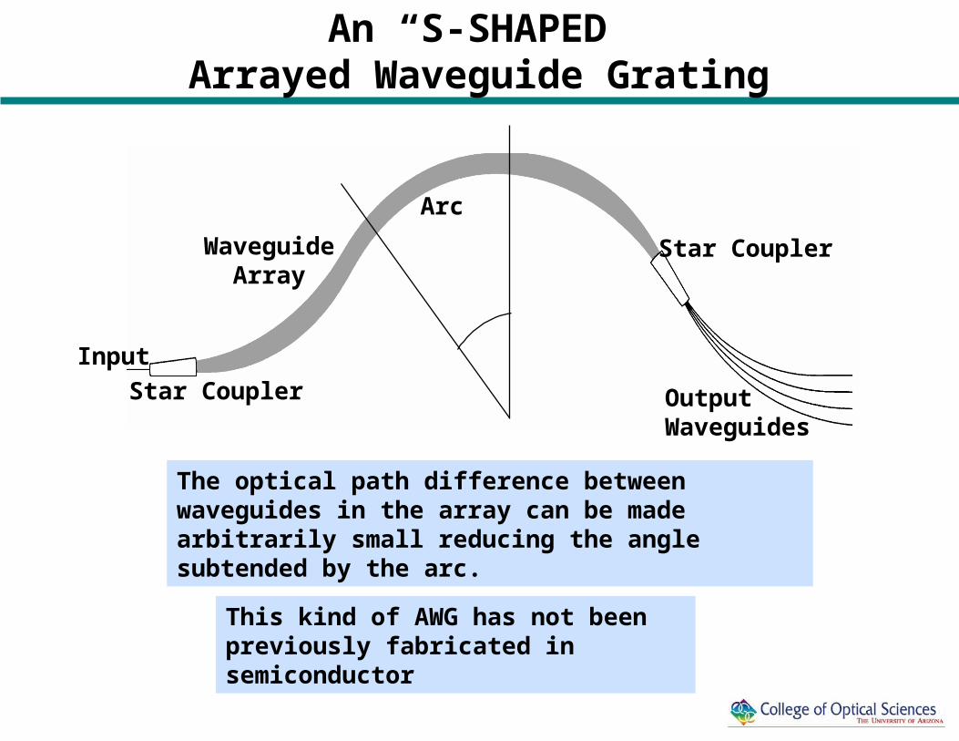
An “S-SHAPED”Arrayed Waveguide Grating
This kind of AWG has not been previously fabricated in semiconductor
The optical path difference between waveguides in the array can be made arbitrarily small reducing the angle subtended by the arc.
Arc
Star Coupler
Star Coupler
OutputWaveguides
WaveguideArray
Input

Shallow Ridge Waveguides
0
2
4
6
8
10
0 1000 2000 3000 4000 5000 6000 7000 8000
Bend radius range for AWGsB
end
Lo
ss (
db
/cm
)
Bend Radius (m)
FundamentalMode
First HigherOrder Mode
2.5 or 3.5 m
1.45 m
0.11 m 0.30 m
InP
InGaAsP
InP 1.45 m
0.30 m
InP
InGaAsP
InP
Loss = 4.5 dB/cm
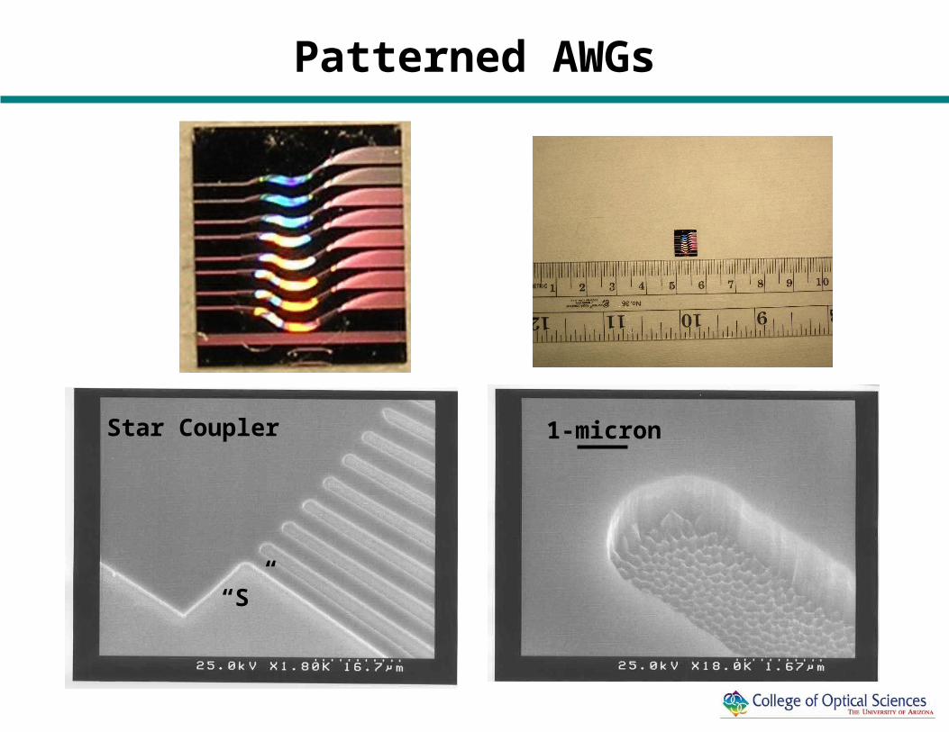
Patterned AWGs
Star Coupler
“S”
1-micron

AWG Response
-35
-30
-25
-20
-15
-10
1460
1470
1480
1490
1500
1510
1520
1530
1540
1550
1560
1570
1580
Wavelength (nm)
Tra
nsm
itte
d P
ow
er (
dB
)
Channel Width ~ 7 nm (FWHM)Cross talk ~ - 15 dB or less
Channel3
4 5 6 7 8 1
1473 15091527
154615621490
Proper AWG design should include chromatic dispersion
Yurt, Rausch, Kost, Peyghambarian, Opt. Express 13, 5535 (2005)
L small Insensitivityto dimensional
error

AWG/SOA Concept
1 cm
AWG A passive device
4SOAs
Active devices
4
InP Substrate
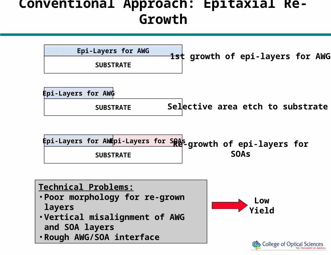
Conventional Approach: Epitaxial Re-Growth
Epi-Layers for AWG
SUBSTRATE
Epi-Layers for AWG
SUBSTRATE
Epi-Layers for AWG
SUBSTRATE
Epi-Layers for SOAs
1st growth of epi-layers for AWG
Selective area etch to substrate
Re-growth of epi-layers forSOAs
Technical Problems:• Poor morphology for re-grown layers• Vertical misalignment of AWG and SOA
layers• Rough AWG/SOA interface
LowYield

Ion-Induced Band Gap Modification
HEAT
ION MASK
BARRIER
QUANTUM WELL
BARRIER
DEFECT
HIGH ENERGY IONS
DIFFUSION
AB
SO
RP
TIO
N C
OE
FF
ICIE
NT
PHOTON ENERGY
ABSORPTIONEDGE
BLUE SHIFT
Advantage-No re-growth
Disadvantage- Constraints on layers

AMPLIFIER BANDWIDTH
Useful amplification range forSemiconductor Optical Amplifier
(or Erbium-Doped Fiber Amplifier)
SOA bandwidth is insufficient to cover all CWDM wavelengths
340 nm (1270 – 1610 nm)
= 20 nm

QUANTUM WELL INTERMIXINGTO ADJUST AMPLIFICATION RANGE
4
4
AB
SO
RP
TIO
N C
OE
FF
ICIE
NT ABSORPTION
EDGE
BLUE SHIFT
4321
Candidates Materials
• InGaAsP - conventional material, limited tuning range• GaInNAs• GaAsSb

GaSb MATERIALS FOR 1.5 MICRON DEVICES
GaAs
LATTICE CONSTANT IN ANGSTROMS
0.5
1.0
1.5
2.0
5.6 5.7 5.8 5.9 6.0 6.1 6.2
BA
ND
GA
P W
AV
EL
EN
GT
H(M
ICR
ON
S)
2.5
3.0
3.5
Substrate
AlSb
GaSb
AlGaSb
GaAsSb
Candidates
AlGaSb(nearly indirect band gap)
GaSb Quantum Wells(indirect gap)
GaAsSb Quantum Wells

GaASSb/AlSb Quantum Wells
G.Griffiths, K.Mohanned, S.Subbana, H.Kroemer and J.L.Merz, Appl. Phys. Lett. 43, 1059 (1983)
L
Г
X
L
Г
X
AddingQuantum
Confinement
Indirect band gap
GaSb
Adding As + Quantum
Confinement
GaAsSb

GaAsSb Quantum Wells
Photoluminescence increases dramatically with As content
1200 1300 1400 1500 1600 1700 1800
0.00
0% AsSb1690
9.1% As
GaAsSb/AlSbQuantum Wells
15.1% As
18.8% As
31% AsSb1704
Sb1707
Sb1720
Sb1682
Ph
oto
lum
ines
cen
ce (
arb
. un
its)
Wavelength (nm)
x 10
GaSb Cap
AlSb
GaAsxSb1-x
AlSb
GaSb Substrate
60X
Kost, Sun, Peyghambarian, Eradat, Selvig, Fimland, and Chow, Appl. Phys. Lett. 85, 5631 (2004).

GaAsSb Quantum Wells
The shift is the largest for any quantum wells (in the telecom band)
= 140 nm, E = 86 meV = 195 nm, E = 123 meV
BORON ION IMPLANTATION (~300 keV, 3x1013 cm-2)
Sun, Peyghambarian, Kost, Eradat, Appl. Phys. Lett. 86, (2005)

Summary
• AWG for CWDM
→ Demonstrated first semiconductor AWGs for CWDM using an flexible “S-shape”
• Band Gap Modification for Heterogeneous Integration
→ GaAsSb/AlSb quantum wells show promise
(enabling technology for PICs)
(lower cost devices)

Future Directions
• Application for CWDM AWG- Combined wavelength and time-division
multiplexing
• New materials for intermixing- GaInNAs- Sb quantum wells on InP
© 1998 - 2005 Christian L. Deichert