Embed Size (px)
Citation preview
[AK8854VQ]
MS0973-E-03 1 2009/05
AK8854VQMulti-Format Digital Video Decoder
Overview
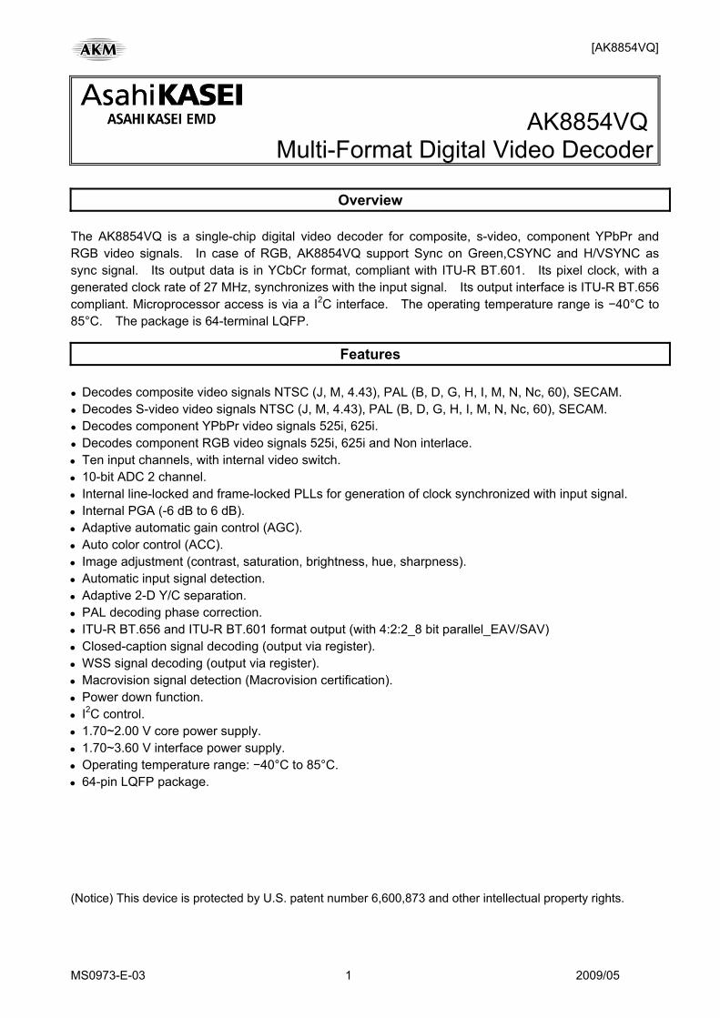
The AK8854VQ is a single-chip digital video decoder for composite, s-video, component YPbPr and RGB video signals. In case of RGB, AK8854VQ support Sync on Green,CSYNC and H/VSYNC as sync signal. Its output data is in YCbCr format, compliant with ITU-R BT.601. Its pixel clock, with a generated clock rate of 27 MHz, synchronizes with the input signal. Its output interface is ITU-R BT.656 compliant. Microprocessor access is via a I2C interface. The operating temperature range is −40°C to 85°C. The package is 64-terminal LQFP.
Features
Decodes composite video signals NTSC (J, M, 4.43), PAL (B, D, G, H, I, M, N, Nc, 60), SECAM. Decodes S-video video signals NTSC (J, M, 4.43), PAL (B, D, G, H, I, M, N, Nc, 60), SECAM. Decodes component YPbPr video signals 525i, 625i. Decodes component RGB video signals 525i, 625i and Non interlace. Ten input channels, with internal video switch. 10-bit ADC 2 channel. Internal line-locked and frame-locked PLLs for generation of clock synchronized with input signal. Internal PGA (-6 dB to 6 dB). Adaptive automatic gain control (AGC). Auto color control (ACC). Image adjustment (contrast, saturation, brightness, hue, sharpness). Automatic input signal detection. Adaptive 2-D Y/C separation. PAL decoding phase correction. ITU-R BT.656 and ITU-R BT.601 format output (with 4:2:2_8 bit parallel_EAV/SAV) Closed-caption signal decoding (output via register). WSS signal decoding (output via register). Macrovision signal detection (Macrovision certification). Power down function. I2C control. 1.70~2.00 V core power supply. 1.70~3.60 V interface power supply. Operating temperature range: −40°C to 85°C. 64-pin LQFP package.
(Notice) This device is protected by U.S. patent number 6,600,873 and other intellectual property rights.
[AK8854VQ]
MS0973-E-03 2 2009/05
1. Functional block diagram [General block diagram]
TEST LOGIC
Microprocessor Interface
PGA2
AAF
CLAMP
MUX
VREF
AVSSAVDD DVDD DVSS PVDD1 PVDD2 VCOM VRN IREFATIO VRP
AIN6
AIN5
AIN4
AIN3 CLAMP
CLAMP
MUX
PGA1
10-bit ADC
AAF
AAF
DecimationFilter
Sync Separation
LuminanceProcess
V Process
U Process
OutputBuffer
VBI Decoding
Clock Module
Timing ControllerDigital PLL
10-bit ADC
AIN10
AIN9
AIN8
AIN7
AIN2
AIN1 HD
VD_F
DVALID_F
NSIG
DTCLK
DATA[7:0]
RGB / YUV
Convert
TEST0 TEST1 VSYNC H_CSYNC SELA RSTNPDNSDA SCLXTI XTO CLKMD OE
[AK8854VQ]
MS0973-E-03 3 2009/05
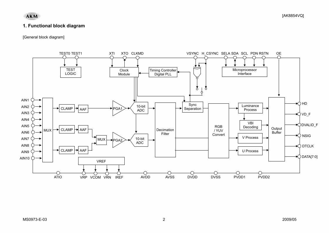
[CVBS decode block diagram]
TEST LOGIC
Microprocessor Interface
AAF
MUX
VREF
AVSSAVDD DVDD DVSS PVDD1 PVDD2VCOM VRN IREFATIO VRP
AIN
TEST0 TEST1
CLAMP PGA1
DecimationFilter
LuminanceProcess
V Process
U Process
OutputBuffer
VBI Decoding
Clock Module
Timing ControllerDigital PLL
10-bit ADC
CVBS
CVBS
C
Y
V
U
VSYNC H_CSYNC SELA RSTNPDNSDA SCLXTI XTO CLKMD
HD
VD_F
DVALID_F
NSIG
DTCLK
DATA[7:0]
OE
YC Separation
Sync Separation
Chrominance
Process
[AK8854VQ]
MS0973-E-03 4 2009/05
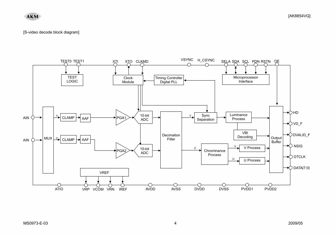
[S-video decode block diagram]
TEST LOGIC
Microprocessor Interface
PGA2
AAF
CLAMP
MUX
VREF
AVSSAVDD DVDD DVSS PVDD1 PVDD2VCOM VRN IREFATIO VRP
AIN
AIN
TEST0 TEST1
CLAMP PGA1
10-bit ADC
AAF
DecimationFilter
LuminanceProcess
V Process
U Process
OutputBuffer
VBI Decoding
Clock Module
Timing ControllerDigital PLL
10-bit ADC
Y
C
V
VSYNC H_CSYNC SELA RSTNPDNSDA SCLXTI XTO CLKMD
HD
VD_F
DVALID_F
NSIG
DTCLK
DATA[7:0]
OE
C
Y Sync Separation
Chrominance
Process U
[AK8854VQ]
MS0973-E-03 5 2009/05
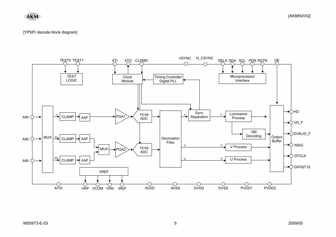
[YPbPr decode block diagram]
TEST LOGIC
Microprocessor Interface
PGA2
AAF
CLAMP
MUX
VREF
AVSSAVDD DVDD DVSS PVDD1 PVDD2VCOM VRN IREFATIO VRP
AIN
AIN
AIN
TEST0 TEST1
CLAMP
CLAMP
MUX
PGA1
10-bit ADC
AAF
AAF
DecimationFilter
Sync Separation
LuminanceProcess
V Process
U Process
OutputBuffer
VBI Decoding
Clock Module
Timing ControllerDigital PLL
10-bit ADC
Y
Pr
Pb
Y
V
U
Y
V
U
VSYNC H_CSYNCSELA RSTNPDNSDA SCLXTI XTO CLKMD
HD
VD_F
DVALID_F
NSIG
DTCLK
DATA[7:0]
OE
[AK8854VQ]
MS0973-E-03 6 2009/05
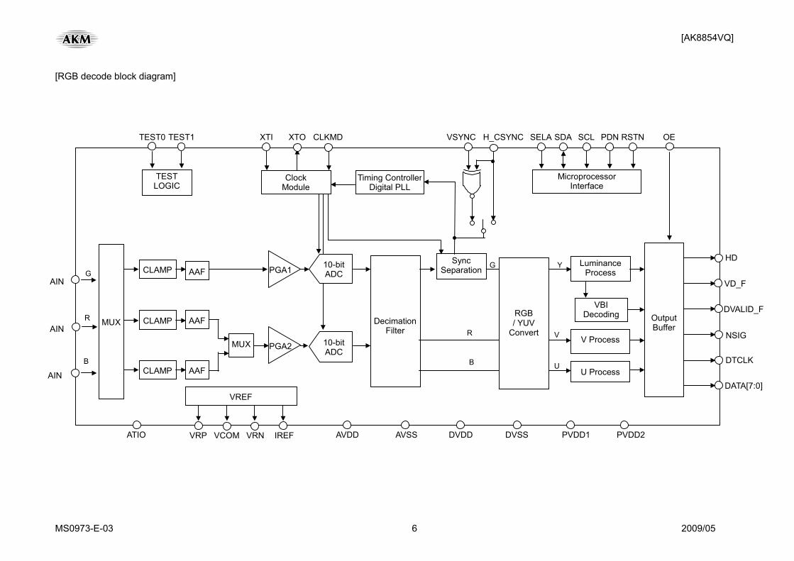
[RGB decode block diagram]
TEST LOGIC
Microprocessor Interface
PGA2
AAF
CLAMP
MUX
VREF
AVSSAVDD DVDD DVSS PVDD1 PVDD2VCOM VRN IREFATIO VRP
CLAMP
CLAMP
MUX
PGA1
10-bit ADC
AAF
AAF
DecimationFilter
Sync Separation
LuminanceProcess
V Process
U Process
OutputBuffer
VBI Decoding
Clock Module
Timing ControllerDigital PLL
10-bit ADC
AIN
AIN
AIN
HD
VD_F
DVALID_F
NSIG
DTCLK
DATA[7:0]
RGB / YUV
Convert
TEST0 TEST1 VSYNC H_CSYNC SELA RSTNPDNSDA SCLXTI XTO CLKMD OE
G
R
B
G
R
B
Y
V
U
[AK8854VQ]
MS0973-E-03 7 2009/05
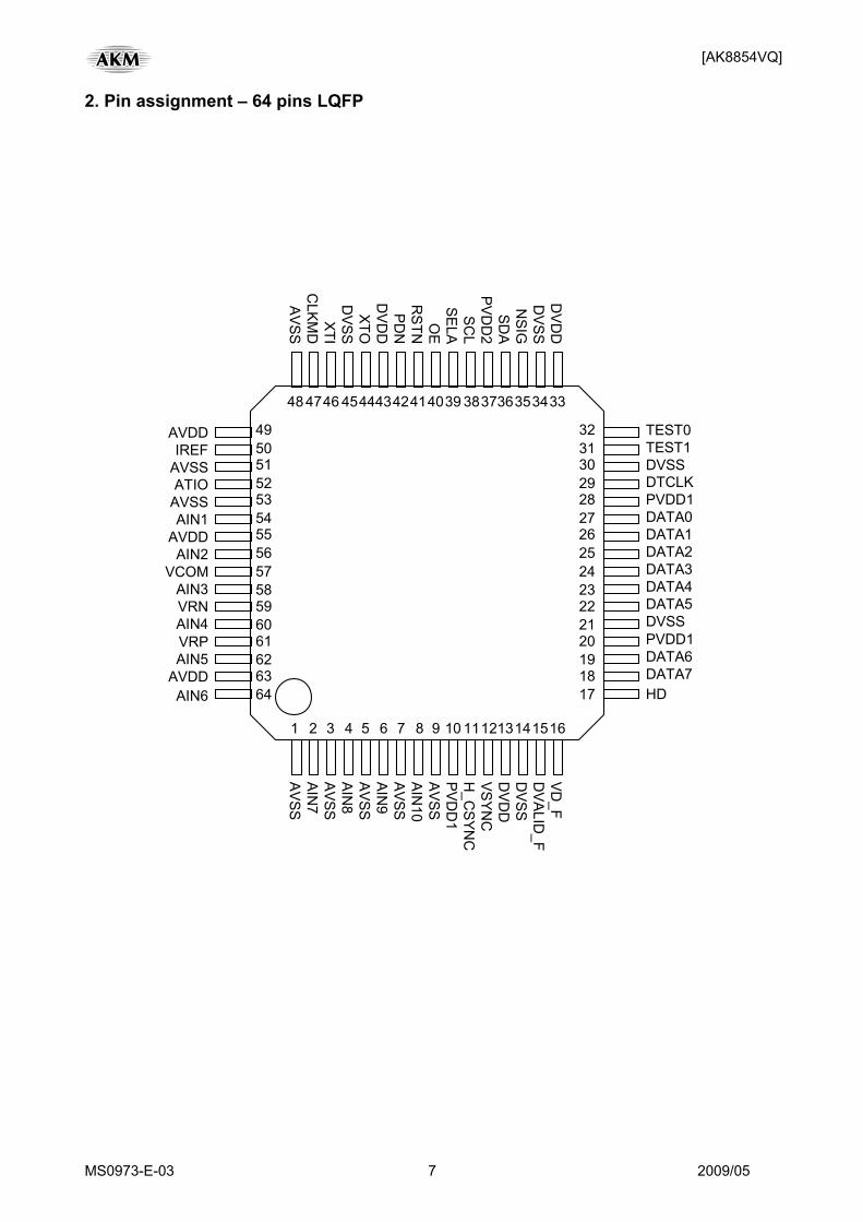
2. Pin assignment – 64 pins LQFP
1 2 3 4 5 6 7 8 9 10 111213141516
39 38373635343346 45444342414048 47
17181920212223242526272829303132
64 63 62 61 60 59 58 57 56 55 54 53 52 51 50 49
AIN2
AIN1AVDD
VCOMAIN3VRNAIN4VRP
AVDDAIN6
AIN5
AVSS
AVDD
AVSSIREF
ATIO
DATA2
DATA0 DATA1
DATA3 DATA4 DATA5 DVSS PVDD1
DATA7 HD
DATA6
PVDD1
TEST0
DVSS TEST1
DTCLK
DVSS
CLKM
DXTI
XTOD
VDD
PDN
RSTN
OE
SELASC
LPVD
D2
SDA
NSIG
DVSS
DVD
D
AVSS
AIN8
AIN7
AVSS
AVSS AIN
9 AVSS AIN
10 AVSS PVD
D1
H_C
SYNC
VSYNC
D
VDD
D
VSS D
VALID_F
VD_F
AVSS
[AK8854VQ]
MS0973-E-03 8 2009/05
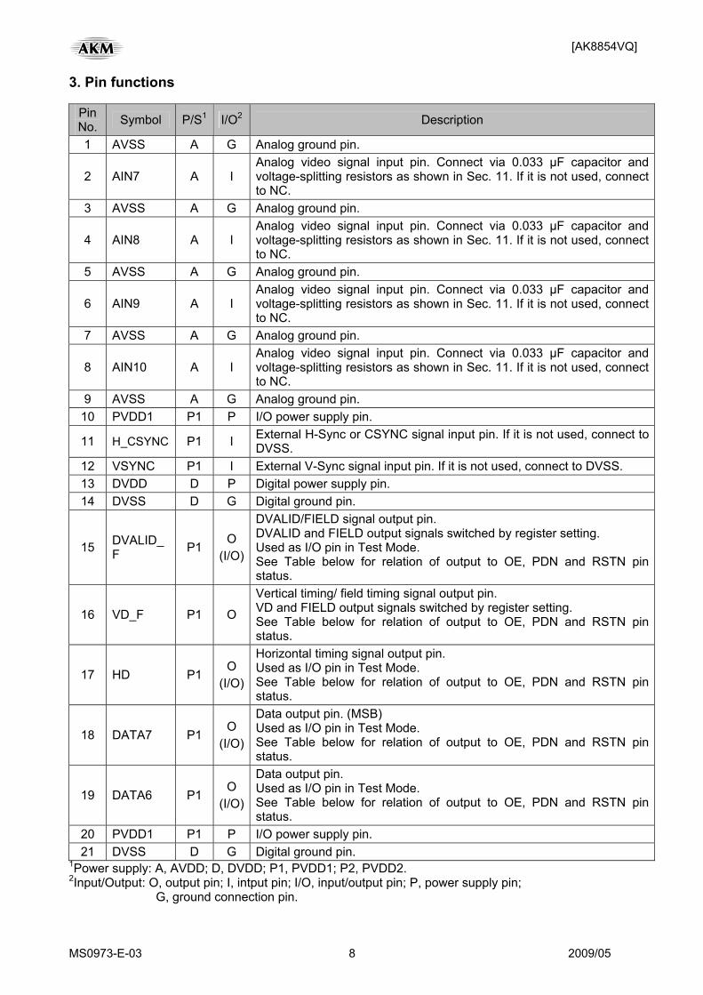
3. Pin functions
Pin No. Symbol P/S1 I/O2 Description
1 AVSS A G Analog ground pin.
2 AIN7 A I Analog video signal input pin. Connect via 0.033 µF capacitor and voltage-splitting resistors as shown in Sec. 11. If it is not used, connect to NC.
3 AVSS A G Analog ground pin.
4 AIN8 A I Analog video signal input pin. Connect via 0.033 µF capacitor and voltage-splitting resistors as shown in Sec. 11. If it is not used, connect to NC.
5 AVSS A G Analog ground pin.
6 AIN9 A I Analog video signal input pin. Connect via 0.033 µF capacitor and voltage-splitting resistors as shown in Sec. 11. If it is not used, connect to NC.
7 AVSS A G Analog ground pin.
8 AIN10 A I Analog video signal input pin. Connect via 0.033 µF capacitor and voltage-splitting resistors as shown in Sec. 11. If it is not used, connect to NC.
9 AVSS A G Analog ground pin. 10 PVDD1 P1 P I/O power supply pin.
11 H_CSYNC P1 I External H-Sync or CSYNC signal input pin. If it is not used, connect to DVSS.
12 VSYNC P1 I External V-Sync signal input pin. If it is not used, connect to DVSS. 13 DVDD D P Digital power supply pin. 14 DVSS D G Digital ground pin.
15 DVALID_F P1
O (I/O)
DVALID/FIELD signal output pin. DVALID and FIELD output signals switched by register setting. Used as I/O pin in Test Mode. See Table below for relation of output to OE, PDN and RSTN pin status.
16 VD_F P1 O
Vertical timing/ field timing signal output pin. VD and FIELD output signals switched by register setting. See Table below for relation of output to OE, PDN and RSTN pin status.
17 HD P1 O
(I/O)
Horizontal timing signal output pin. Used as I/O pin in Test Mode. See Table below for relation of output to OE, PDN and RSTN pin status.
18 DATA7 P1 O
(I/O)
Data output pin. (MSB) Used as I/O pin in Test Mode. See Table below for relation of output to OE, PDN and RSTN pin status.
19 DATA6 P1 O
(I/O)
Data output pin. Used as I/O pin in Test Mode. See Table below for relation of output to OE, PDN and RSTN pin status.
20 PVDD1 P1 P I/O power supply pin. 21 DVSS D G Digital ground pin.
1Power supply: A, AVDD; D, DVDD; P1, PVDD1; P2, PVDD2. 2Input/Output: O, output pin; I, intput pin; I/O, input/output pin; P, power supply pin;
G, ground connection pin.
[AK8854VQ]
MS0973-E-03 9 2009/05
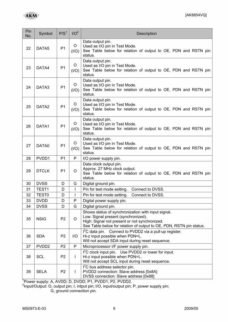
PinNo. Symbol P/S1 I/O2 Description
22 DATA5 P1 O
(I/O)
Data output pin. Used as I/O pin in Test Mode. See Table below for relation of output to OE, PDN and RSTN pin status.
23 DATA4 P1 O
(I/O)
Data output pin. Used as I/O pin in Test Mode. See Table below for relation of output to OE, PDN and RSTN pin status.
24 DATA3 P1 O
(I/O)
Data output pin. Used as I/O pin in Test Mode. See Table below for relation of output to OE, PDN and RSTN pin status.
25 DATA2 P1 O
(I/O)
Data output pin. Used as I/O pin in Test Mode. See Table below for relation of output to OE, PDN and RSTN pin status.
26 DATA1 P1 O
(I/O)
Data output pin. Used as I/O pin in Test Mode. See Table below for relation of output to OE, PDN and RSTN pin status.
27 DATA0 P1 O
(I/O)
Data output pin. Used as I/O pin in Test Mode. See Table below for relation of output to OE, PDN and RSTN pin status.
28 PVDD1 P1 P I/O power supply pin.
29 DTCLK P1 O
Data clock output pin. Approx. 27 MHz clock output. See Table below for relation of output to OE, PDN and RSTN pin status.
30 DVSS D G Digital ground pin. 31 TEST1 D I Pin for test mode setting. Connect to DVSS. 32 TEST0 D I Pin for test mode setting. Connect to DVSS. 33 DVDD D P Digital power supply pin. 34 DVSS D G Digital ground pin.
35 NSIG P2 O
Shows status of synchronization with input signal. Low: Signal present (synchronized). High: Signal not present or not synchronized. See Table below for relation of output to OE, PDN, RSTN pin status.
36 SDA P2 I/O I2C data pin. Connect to PVDD2 via a pull-up register. Hi-z input possible when PDN=L. Will not accept SDA input during reset sequence.
37 PVDD2 P2 P Microprocessor I/F power supply pin.
38 SCL P2 I I2C clock input pin. Use PVDD2 or lower for input. Hi-z input possible when PDN=L. Will not accept SCL input during reset sequence.
39 SELA P2 I I2C bus address selector pin. PVDD2 connection: Slave address [0x8A] DVSS connection: Slave address [0x88]
1Power supply: A, AVDD; D, DVDD; P1, PVDD1; P2, PVDD2. 2Input/Output: O, output pin; I, intput pin; I/O, input/output pin; P, power supply pin;
G, ground connection pin.
[AK8854VQ]
MS0973-E-03 10 2009/05
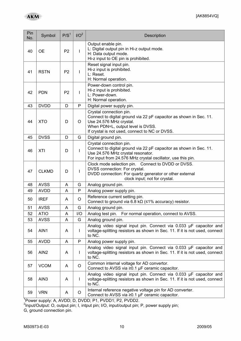
PinNo. Symbol P/S1 I/O2 Description
40 OE P2 I
Output enable pin. L: Digital output pin in Hi-z output mode. H: Data output mode. Hi-z input to OE pin is prohibited.
41 RSTN P2 I
Reset signal input pin. Hi-z input is prohibited. L: Reset. H: Normal operation.
42 PDN P2 I
Power-down control pin. Hi-z input is prohibited. L: Power-down. H: Normal operation.
43 DVDD D P Digital power supply pin.
44 XTO D O
Crystal connection pin. Connect to digital ground via 22 pF capacitor as shown in Sec. 11. Use 24.576 MHz crystal. When PDN=L, output level is DVSS. If crystal is not used, connect to NC or DVSS.
45 DVSS D G Digital ground pin.
46 XTI D I
Crystal connection pin. Connect to digital ground via 22 pF capacitor as shown in Sec. 11. Use 24.576 MHz crystal resonator. For input from 24.576 MHz crystal oscillator, use this pin.
47 CLKMD D I
Clock mode selection pin. Connect to DVDD or DVSS. DVSS connection: For crystal. DVDD connection: For quartz generator or other external clock input; not for crystal.
48 AVSS A G Analog ground pin. 49 AVDD A P Analog power supply pin.
50 IREF A O Reference current setting pin. Connect to ground via 6.8 kΩ (≤1% accuracy) resistor.
51 AVSS A G Analog ground pin. 52 ATIO A I/O Analog test pin. For normal operation, connect to AVSS. 53 AVSS A G Analog ground pin.
54 AIN1 A I Analog video signal input pin. Connect via 0.033 µF capacitor and voltage-splitting resistors as shown in Sec. 11. If it is not used, connect to NC.
55 AVDD A P Analog power supply pin.
56 AIN2 A I Analog video signal input pin. Connect via 0.033 µF capacitor and voltage-splitting resistors as shown in Sec. 11. If it is not used, connect to NC.
57 VCOM A O Common internal voltage for AD convertor. Connect to AVSS via ≥0.1 µF ceramic capacitor.
58 AIN3 A I Analog video signal input pin. Connect via 0.033 µF capacitor and voltage-splitting resistors as shown in Sec. 11. If it is not used, connect to NC.
59 VRN A O Internal reference negative voltage pin for AD converter. Connect to AVSS via ≥0.1 µF ceramic capacitor.
1Power supply: A, AVDD; D, DVDD; P1, PVDD1; P2, PVDD2. 2Input/Output: O, output pin; I, intput pin; I/O, input/output pin; P, power supply pin; G, ground connection pin.
[AK8854VQ]
MS0973-E-03 11 2009/05
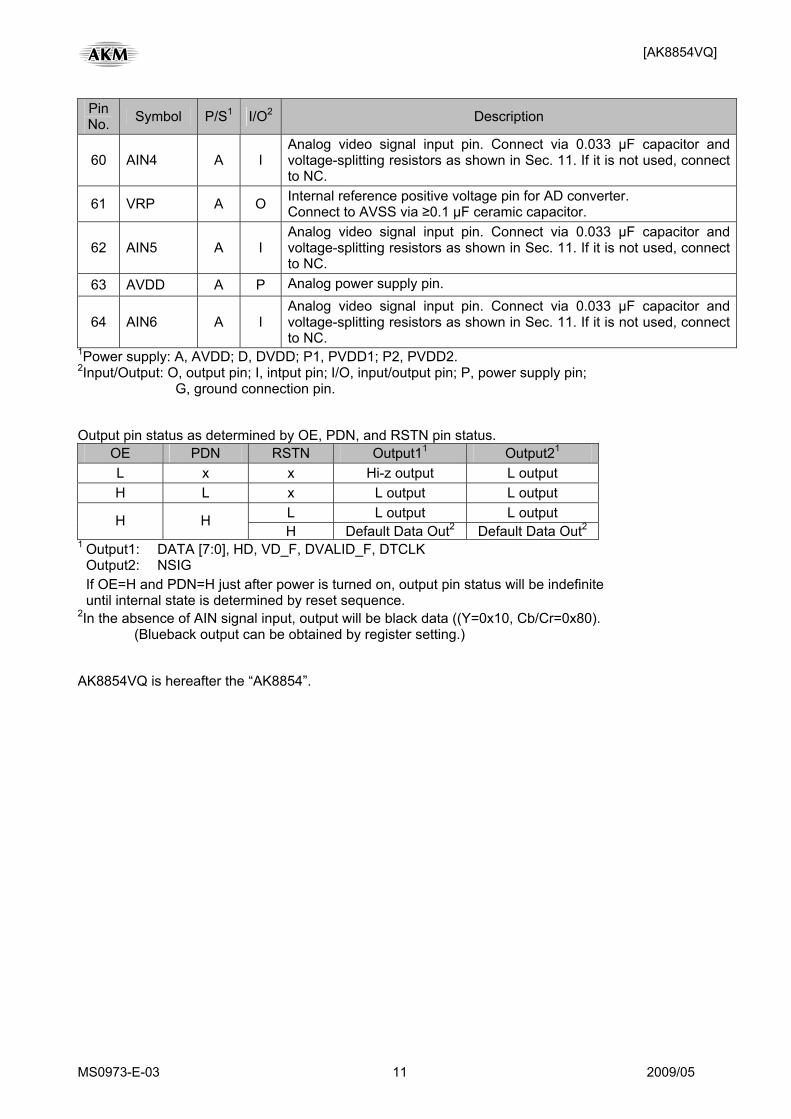
PinNo. Symbol P/S1 I/O2 Description
60 AIN4 A I Analog video signal input pin. Connect via 0.033 µF capacitor and voltage-splitting resistors as shown in Sec. 11. If it is not used, connect to NC.
61 VRP A O Internal reference positive voltage pin for AD converter. Connect to AVSS via ≥0.1 µF ceramic capacitor.
62 AIN5 A I Analog video signal input pin. Connect via 0.033 µF capacitor and voltage-splitting resistors as shown in Sec. 11. If it is not used, connect to NC.
63 AVDD A P Analog power supply pin.
64 AIN6 A I Analog video signal input pin. Connect via 0.033 µF capacitor and voltage-splitting resistors as shown in Sec. 11. If it is not used, connect to NC.
1Power supply: A, AVDD; D, DVDD; P1, PVDD1; P2, PVDD2. 2Input/Output: O, output pin; I, intput pin; I/O, input/output pin; P, power supply pin;
G, ground connection pin. Output pin status as determined by OE, PDN, and RSTN pin status.
OE PDN RSTN Output11 Output21 L x x Hi-z output L output H L x L output L output
L L output L output H H H Default Data Out2 Default Data Out2
1 Output1: DATA [7:0], HD, VD_F, DVALID_F, DTCLK Output2: NSIG If OE=H and PDN=H just after power is turned on, output pin status will be indefinite until internal state is determined by reset sequence. 2In the absence of AIN signal input, output will be black data ((Y=0x10, Cb/Cr=0x80). (Blueback output can be obtained by register setting.) AK8854VQ is hereafter the “AK8854”.
[AK8854VQ]
MS0973-E-03 12 2009/05
4. Electrical specifications 4.1 Absolute maximum ratings
Parameter Min Max Units Notes Supply voltage DVDD, AVDD
PVDD1 , PVDD2
−0.3 −0.3
2.2 4.2
V V
–
Analog input pin voltage A (VinA) −0.3 AVDD + 0.3 (≤2.2) V –
Digital input pin voltage D (VinD) −0.3 DVDD + 0.3 (≤2.2) V
XTI, XTO, CLKMD, TEST0, TEST1
Digital output pin voltage P1 (VoutP)
−0.3 PVDD1 + 0.3 (≤4.2) V DTCLK, DATA[7:0], HD,
VD_F, DVALID_F, H_CSYNC, VSYNC
Digital input pin current P2 (VinP) −0.3 PVDD2 + 0.3 (≤4.2) V
OE, SELA, PDN, RSTN,SDA, SCL, NSIG
Input pin current (Iin) (except for power supply pin) −10 10 mA –
Storage temperature −40 125 ˚C – The above supply voltages are referenced to ground pins (DVSS=AVSS) at 0 V (the Reference Voltage). All power supply grounds (AVSS, DVSS) should be at the same electric potential. If digital output pins are connected to data bus, the data bus operating voltage should be in the same range as shown above for the digital output pin. 4.2 Recommended operating conditions
Parameter Min Typ Max Units Condition Analog supply voltage (AVDD) Digital supply voltage (DVDD) 1.70 1.80 2.00 V AVDD=DVDD
I/O supply voltage (PVDD1) MPU I/F supply voltage (PVDD2) 1.70 1.80 3.60 V
PVDD1≥DVDD PVDD2≥DVDD
Operating temp. (Ta) −40 – 85 ˚C – The above supply voltages are referenced to ground pins (DVSS=AVSS) at 0 V (the Reference Voltage). All power supply grounds (AVSS, DVSS) should be at the same electric potential.
[AK8854VQ]
MS0973-E-03 13 2009/05
4.3 DC characteristics Where no specific condition is indicated in the following table, the supply voltage range is the same as that shown for the recommended operating conditions in 4-2 above.
Parameter Symbol Min Typ Max Units Condition
0.8PVDD2 – – V Case 1a Digital P2 input high
voltage VIH 0.7PVDD2 – – V Case 2b
– – 0.2PVDD2 V Case 1a Digital P2 input low
voltage VIL – – 0.3PVDD2 V Case 2b
Digital D input high voltage VDIH 0.8DVDD – – V –
Digital D input low voltage VDIL – – 0.2DVDD V –
0.8PVDD1 – – V Case 1a Digital input high voltage VIH
0.7PVDD1 – – V Case 2b
– – 0.2PVDD1 V Case 1a Digital input low voltage VIL
– – 0.3PVDD1 V Case 2b
Digital input leak current IL – – ±10 uA – Digital P1 output high
voltage VOH 0.7PVDD1 – – V IOH = −600uA
Digital P1 output low voltage VOL – – 0.3PVDD1 V IOL = 1mA
Digital P2 output high voltage VOH 0.7PVDD2 – – V IOH = −600uA
Digital P2 output low voltage VOL – – 0.3PVDD2 V IOL = 1mA
I2C (SDA)L output VOLC – –
0.4 0.2PVDD2
V IOLC = 3mA PVDD2≥2.0V PVDD2<2.0V
aDVDD = 1.70V~2.00V, 1.70V≤PVDD1<2.70V, 1.70V≤PVDD2<2.70V, Ta: −40~85˚C bDVDD = 1.70V~2.00V, 2.70V≤PVDD1≤3.60V, 2.70V≤PVDD2≤3.60V, Ta: −40~85˚C
Definition of above input/output terms Digital P2 input: Collective term for SDA, SCL, SELA, OE, PDN, RSTN pin inputs. Digital D input: Collective term for CLKMD, TEST0, TEST1 pin inputs.
Digital input: Collective term for H_CSYNC, VSYNC pin inputs. Digital P1 output: Collective term for DTCLK, DATA[7:0], HD, VD_F, DVALID_F pin outputs.
Digital P2 output: Collective term for NSIG pin outputs. SDA pin output: Not termed digital pin output unless otherwise specifically stated.
[AK8854VQ]
MS0973-E-03 14 2009/05
4.4 Analog characteristics (AVDD=1.8V, Temp.25˚C) Selector clamp
Parameter Symbol Min Typ Max Units Condition
Maximum input range VIMX 0 0.50 0.60 VPP
Max value at minimum PGA_GAIN setting.
Typical value at default PGA_GAIN setting.
PGA
Parameter Symbol Min Typ Max Units Resolution – 7 – bits
Minimum gain GMN – −6 – dB Maximum gain GMX – 6 – dB
Gain step GST – 0.094 0.235 dB AD converter
Parameter Symbol Min Typ Max Units Condition Resolution RES 10 bits –
Operating clock frequency FS – 27 – MHz –
Integral nonlinearity INL – 2.0 4.0 LSB FS = 27 MHz, PGA_GAIN default setting
Differential nonlinearity DNL – 1.0 2.0 LSB FS = 27 MHz, PGA_GAIN default setting
S/N SN – 53 – dB Fin = 1 MHz*, FS = 27 MHz,PGA_GAIN default setting
S/(N+D) SND – 51 – dB Fin=1MHz*, FS=27MHz PGA_GAIN default setting
Full scale Gain matching IFGM 5 PGA_GAIN default setting ADC internal common
voltage VCOM – 0.9 – V –
ADC internal positive VREF VRP – 1.1 – V –
ADC internal negative VREF VRN – 0.7 – V –
*Fin = AIN input signal frequency AAF (Anti-Aliasing Filter)
Parameter Symbol Min Typ Max Units Condition
Pass band ripple Gp −1 +1 dB 6 MHz Stop band blocking Gs 10 22 – dB 27 MHz
[AK8854VQ]
MS0973-E-03 15 2009/05
4.5 Current consumption (at DVDD = AVDD = PVDD1 = PVDD2 = 1.8V, Ta = −40 ~ 85˚C) Parameter Symbol Min Typ Max Units Condition
(Active mode) Total IDD 108 145 mA RGB/YPbPr: 3ch
82 mA RGB/YPbPr: 3ch (63) mA YC: 2ch(*1)
Analog block
AIDD
(34) mA CVBS: 1ch(*1)
Digital block DIDD 22 mA I/O block PIDD 4 mA
With crystal connected Load condition: CL=15pF(*2)
(Power down mode) Total SIDD ≤ 1 100 uA Analog block ASIDD ≤ 1 uA Digital block DSIDD ≤ 1 uA I/O block PSIDD ≤ 1 uA
PDN=L(DVSS)
(*1) Reference Value (*2) With NTSC-J 100% color bar input. 4.6 Crystal circuit block (Ta: −40~85˚C, CLKMD-pin is connected to DVSS.)
Parameter Symbol Min Typ Max Units Notes Frequency f0 – 24.576 – MHz –
Frequency tolerance Δf/f – ±100 ppm – Load capacitance CL – 15 – pF –
Effective equivalent resistance Re – – 100 Ω See note 1 Crystal parallel capacitance CO – 0.9 – pF –
XTI terminal external connection load capacitance CXI – 22 – pF If CL=15 pF
XTO terminal external connection load capacitance CXO – 22 – pF If CL=15 pF
(note1) Effective equivalent resistance generally may be taken as Re = R1 x (1+CO/CL)2, where R1 is the crystal series equivalent resistance.
Example connection
XTI pin XTO pin
Rf
Rd (note2)
CXI = 22pF CXO = 22pF
AK8854 internal circuit
External circuit
(note2) Determine need for and appropriate value of limiting resistance (Rd) in accordance with
the crystal specifications.
[AK8854VQ]
MS0973-E-03 16 2009/05
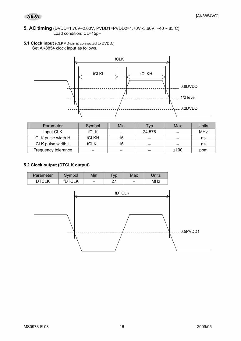
5. AC timing (DVDD=1.70V~2.00V, PVDD1=PVDD2=1.70V~3.60V, −40 ~ 85˚C) Load condition: CL=15pF
5.1 Clock input (CLKMD-pin is connected to DVDD.)
Set AK8854 clock input as follows.
fCLK
tCLKL tCLKH
0.8DVDD
1/2 level
0.2DVDD
Parameter Symbol Min Typ Max Units Input CLK fCLK – 24.576 – MHz
CLK pulse width H tCLKH 16 – – ns CLK pulse width L tCLKL 16 – – ns
Frequency tolerance – – – ±100 ppm 5.2 Clock output (DTCLK output)
Parameter Symbol Min Typ Max Units DTCLK fDTCLK – 27 – MHz
fDTCLK
0.5PVDD1
[AK8854VQ]
MS0973-E-03 17 2009/05
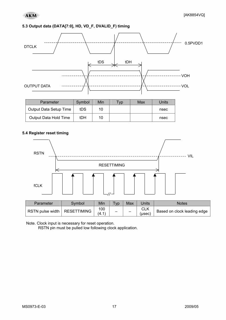
5.3 Output data (DATA[7:0], HD, VD_F, DVALID_F) timing
tDS
0.5PVDD1
tDH
VOH
VOL
DTCLK
OUTPUT DATA
Parameter Symbol Min Typ Max Units
Output Data Setup Time tDS 10 nsec
Output Data Hold Time tDH 10 nsec 5.4 Register reset timing
RESETTIMING
RSTN
fCLK
VIL
Parameter Symbol Min Typ Max Units Notes
RSTN pulse width RESETTIMING 100 (4.1) – – CLK
(µsec) Based on clock leading edge
Note. Clock input is necessary for reset operation.
RSTN pin must be pulled low following clock application.
[AK8854VQ]
MS0973-E-03 18 2009/05
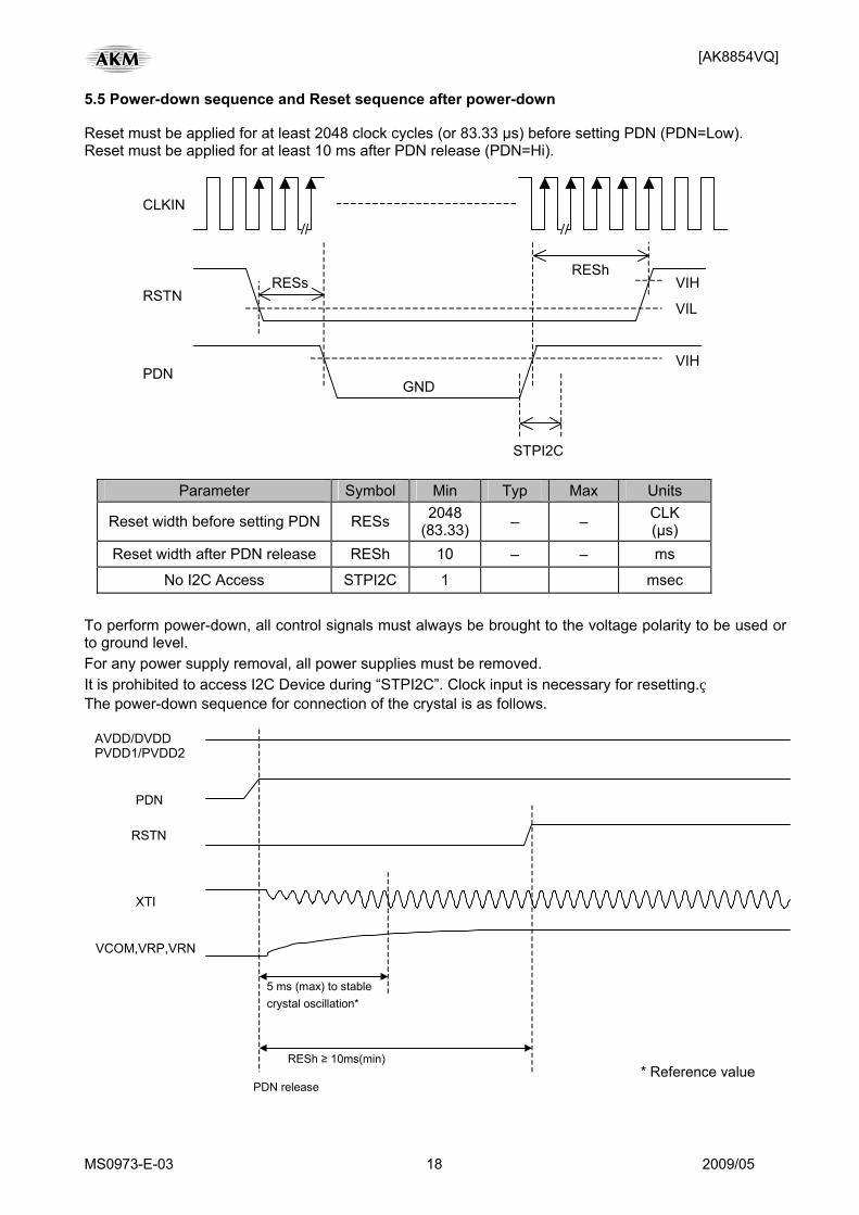
5.5 Power-down sequence and Reset sequence after power-down Reset must be applied for at least 2048 clock cycles (or 83.33 µs) before setting PDN (PDN=Low). Reset must be applied for at least 10 ms after PDN release (PDN=Hi).
VIH
VIL
VIH
CLKIN
RSTN
PDN
RESs RESh
GND
STPI2C
Parameter Symbol Min Typ Max Units
Reset width before setting PDN RESs 2048 (83.33) – – CLK
(µs) Reset width after PDN release RESh 10 – – ms
No I2C Access STPI2C 1 msec To perform power-down, all control signals must always be brought to the voltage polarity to be used or to ground level. For any power supply removal, all power supplies must be removed. It is prohibited to access I2C Device during “STPI2C”. Clock input is necessary for resetting. The power-down sequence for connection of the crystal is as follows. AVDD/DVDD
PVDD1/PVDD2
PDN
RSTN
5 ms (max) to stablecrystal oscillation*
XTI
VCOM,VRP,VRN
PDN release * Reference value
RESh ≥ 10ms(min)
[AK8854VQ]
MS0973-E-03 19 2009/05
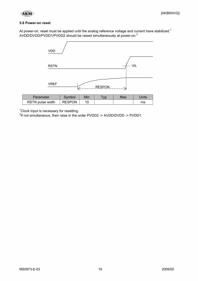
5.6 Power-on reset At power-on, reset must be applied until the analog reference voltage and current have stabilized.1 AVDD/DVDD/PVDD1/PVDD2 should be raised simultaneously at power-on.2
VIL
RESPON VREF
RSTN
VDD
Parameter Symbol Min Typ Max Units RSTN pulse width RESPON 10 ms
1Clock input is necessary for resetting. 2If not simultaneous, then raise in the order PVDD2 -> AVDD/DVDD -> PVDD1.
[AK8854VQ]
MS0973-E-03 20 2009/05
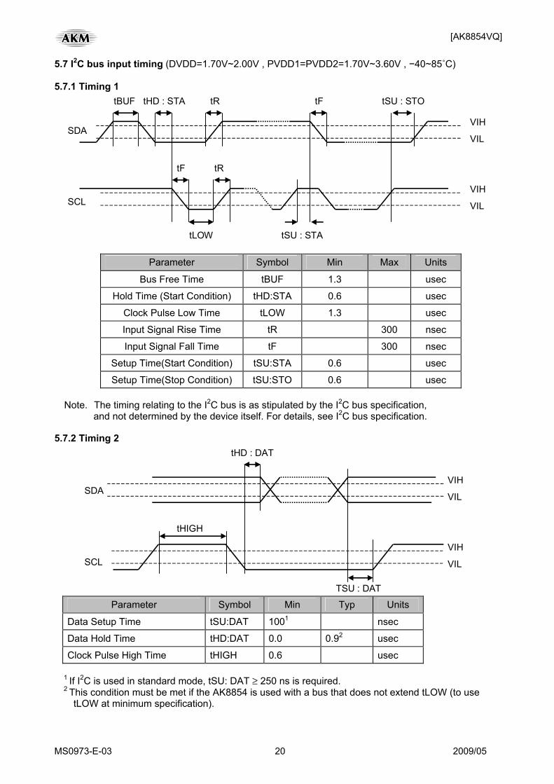
5.7 I2C bus input timing (DVDD=1.70V~2.00V , PVDD1=PVDD2=1.70V~3.60V , −40~85˚C) 5.7.1 Timing 1
tBUF tHD : STA tR tF tSU : STO
VIH
VIL SDA
tF tR
tSU : STAtLOW
VIH
VIL SCL
Parameter Symbol Min Max Units
Bus Free Time tBUF 1.3 usec
Hold Time (Start Condition) tHD:STA 0.6 usec
Clock Pulse Low Time tLOW 1.3 usec
Input Signal Rise Time tR 300 nsec
Input Signal Fall Time tF 300 nsec
Setup Time(Start Condition) tSU:STA 0.6 usec
Setup Time(Stop Condition) tSU:STO 0.6 usec
Note. The timing relating to the I2C bus is as stipulated by the I2C bus specification, and not determined by the device itself. For details, see I2C bus specification.
5.7.2 Timing 2
VIH
VIL SDA
VIH
VILSCL
tHIGH
tHD : DAT
TSU : DAT Parameter Symbol Min Typ Units
Data Setup Time tSU:DAT 1001 nsec
Data Hold Time tHD:DAT 0.0 0.92 usec
Clock Pulse High Time tHIGH 0.6 usec
1 If I2C is used in standard mode, tSU: DAT ≥ 250 ns is required. 2 This condition must be met if the AK8854 is used with a bus that does not extend tLOW (to use
tLOW at minimum specification).
[AK8854VQ]
MS0973-E-03 21 2009/05
6. Functional overview The following key functions are characteristic of the AK8854 and its operational performance.
(1) It accepts composite video signal (CVBS), S-video, component YPbPr and RGB input with 10 input pins available for this purpose. The decode signal is selected via the register.
(2) It contains an internal analog band limiting filter (anti-aliasing) in front of the AD converter input. (3) Its analog circuit clamps the input signal to the sync tip (analog sync tip clamp). Its digital circuit
clamps the digitized input data to the pedestal level (digital pedestal clamp). (4) It decodes NTSC-M, J; NTSC-4.43; PAL-B, D, G, H, I, N; PAL-Nc, PAL-M, PAL-60; and SECAM
video signals, as selected by register setting for input signal category. In auto detection mode, it automatically recognizes the input signal category.
(5) Its VBI data slicing function enables output of the slicing results as ITU-R BT.601 format digital data.
(6) Its adaptive AGC function enables measurement of the input signal size and determination of the input signal level.
(7) Its ACC function enables measurement of the input signal color burst size and determination of the appropriate color burst level.
(8) It performs adaptive two-dimensional Y/C separation, in which its phase detector selects the best correlation from among vertical, horizontal, and diagonal samples and the optimum Y/C separation mode.
(9) Its digital pixel spacing adjustor can align vertical positions by vertical pixel positioning. (10) It operates in line-locked, frame-locked, or fixed clock mode, with automatic transition and optimum
mode selection by automatic scanning. (11) In PAL-B, D, G, H, I, and N decoding, it can perform phase-difference correction for each line. (12) Its decoded data is ITU-R BT.656 compliant, except in certain cases of fixed-clock operation or
poor-quality input signal. (13) For connection of devices having no ITU-R BT.656 interface, it shows the active video region by
DVALID signal output. (14) Its input-stage embedded PGA can be adjusted in the range -6~+6dB by register setting, in gain
steps of approximately 0.1 dB/step. (15) It detects and separates the sync signal from the digitized input signal. The detected sync signal
provides the base timing for decode processing, and the separated sync signal as the basis for calculation of phase error signal and for sampling clock control.
(16) It judges the chroma signal quality from the color burst of the input signal, and can apply color kill if the signal quality is judged insufficient. It can also apply color kill if the color decode PLL lock is lost.
(17) Its image quality adjustment function includes contrast, brightness, hue, color saturation, and sharpness adjustment.
(18) Its luminance band limiting filter is adjustable via register setting. (19) It can provide sepia output of decoded results. (20) It can decode conflated closed caption data, closed caption extended data, VBID(CGMS), and
WSS signals, and write them separately to the storage register. (21) Its monitoring register enables monitoring of a number of internal functions. (22) It enables Macrovision signal type notification, in cases where the Macrovision signal is included in
the decoded data. (23) It enables U/V signal band adjustment, by switching the low pass filter after C signal demodulating. (24) It enables C filter band switching via the register, for Y/C separation.
[AK8854VQ]
MS0973-E-03 22 2009/05
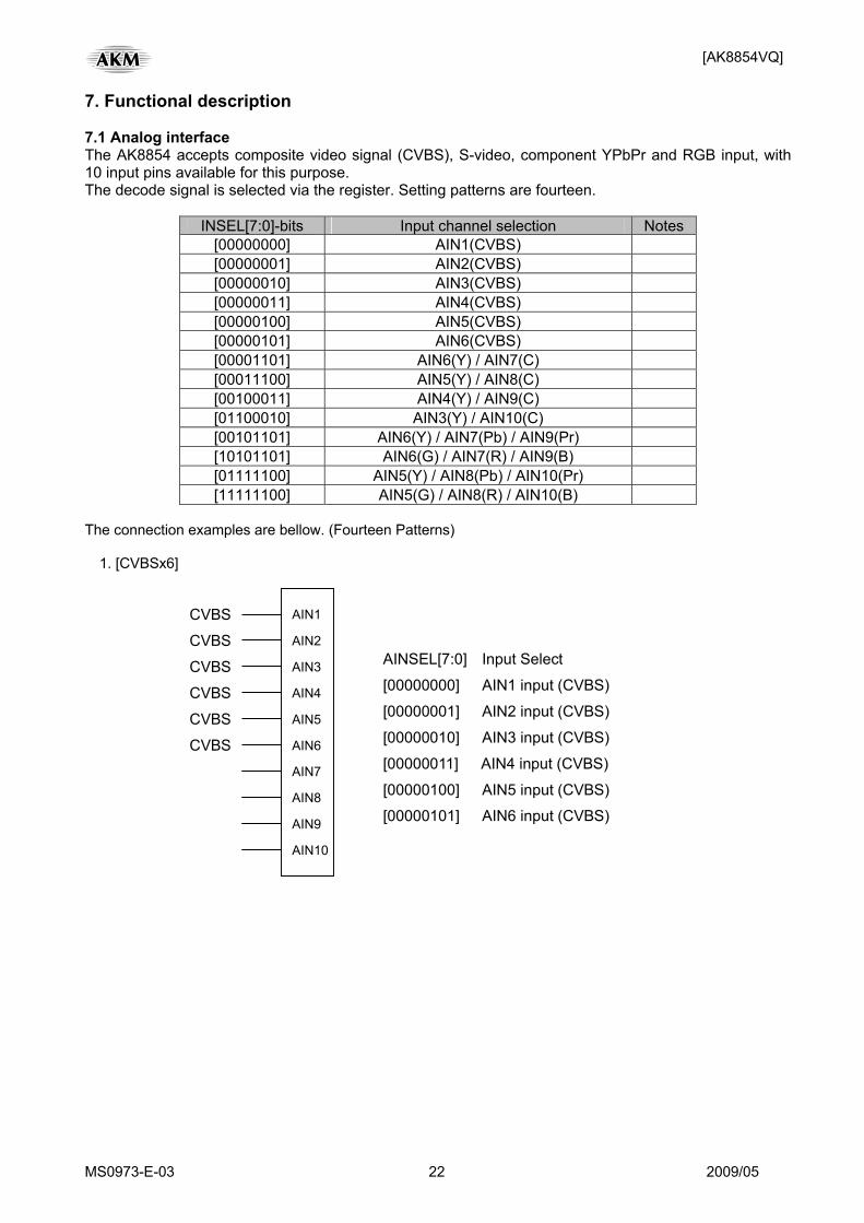
7. Functional description 7.1 Analog interface The AK8854 accepts composite video signal (CVBS), S-video, component YPbPr and RGB input, with 10 input pins available for this purpose. The decode signal is selected via the register. Setting patterns are fourteen.
INSEL[7:0]-bits Input channel selection Notes [00000000] AIN1(CVBS) [00000001] AIN2(CVBS) [00000010] AIN3(CVBS) [00000011] AIN4(CVBS) [00000100] AIN5(CVBS) [00000101] AIN6(CVBS) [00001101] AIN6(Y) / AIN7(C) [00011100] AIN5(Y) / AIN8(C) [00100011] AIN4(Y) / AIN9(C) [01100010] AIN3(Y) / AIN10(C) [00101101] AIN6(Y) / AIN7(Pb) / AIN9(Pr) [10101101] AIN6(G) / AIN7(R) / AIN9(B) [01111100] AIN5(Y) / AIN8(Pb) / AIN10(Pr) [11111100] AIN5(G) / AIN8(R) / AIN10(B)
The connection examples are bellow. (Fourteen Patterns)
1. [CVBSx6]
CVBS
CVBS
CVBS
CVBS
AIN1
AIN2
AIN3
AIN4
AIN5
AIN6
AIN7
AIN8
AIN9
AIN10
AINSEL[7:0] Input Select
[00000000] AIN1 input (CVBS)
[00000001] AIN2 input (CVBS)
[00000010] AIN3 input (CVBS)
[00000011] AIN4 input (CVBS)
[00000100] AIN5 input (CVBS)
[00000101] AIN6 input (CVBS)
CVBS
CVBS
[AK8854VQ]
MS0973-E-03 23 2009/05
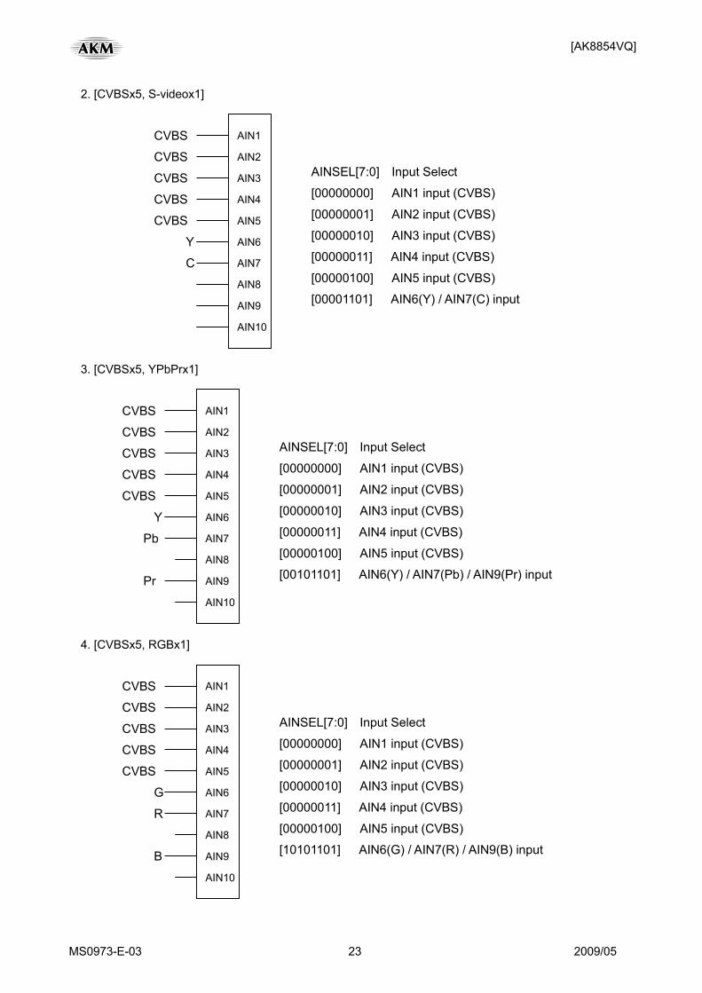
2. [CVBSx5, S-videox1]
Y
CVBS
CVBS
CVBS
CVBS
C
AIN1
AIN2
AIN3
AIN4
AIN5
AIN6
AIN7
AIN8
AIN9
AIN10
AINSEL[7:0] Input Select
[00000000] AIN1 input (CVBS)
[00000001] AIN2 input (CVBS)
[00000010] AIN3 input (CVBS)
[00000011] AIN4 input (CVBS)
[00000100] AIN5 input (CVBS)
[00001101] AIN6(Y) / AIN7(C) input
CVBS
3. [CVBSx5, YPbPrx1]
Y
CVBS
CVBS
CVBS
CVBS
Pb
AIN1
AIN2
AIN3
AIN4
AIN5
AIN6
AIN7
AIN8
AIN9
AIN10
AINSEL[7:0] Input Select
[00000000] AIN1 input (CVBS)
[00000001] AIN2 input (CVBS)
[00000010] AIN3 input (CVBS)
[00000011] AIN4 input (CVBS)
[00000100] AIN5 input (CVBS)
[00101101] AIN6(Y) / AIN7(Pb) / AIN9(Pr) input
CVBS
Pr
4. [CVBSx5, RGBx1]
G
CVBS
CVBS
CVBS
CVBS
R
AIN1
AIN2
AIN3
AIN4
AIN5
AIN6
AIN7
AIN8
AIN9
AIN10
AINSEL[7:0] Input Select
[00000000] AIN1 input (CVBS)
[00000001] AIN2 input (CVBS)
[00000010] AIN3 input (CVBS)
[00000011] AIN4 input (CVBS)
[00000100] AIN5 input (CVBS)
[10101101] AIN6(G) / AIN7(R) / AIN9(B) input
CVBS
B
[AK8854VQ]
MS0973-E-03 24 2009/05
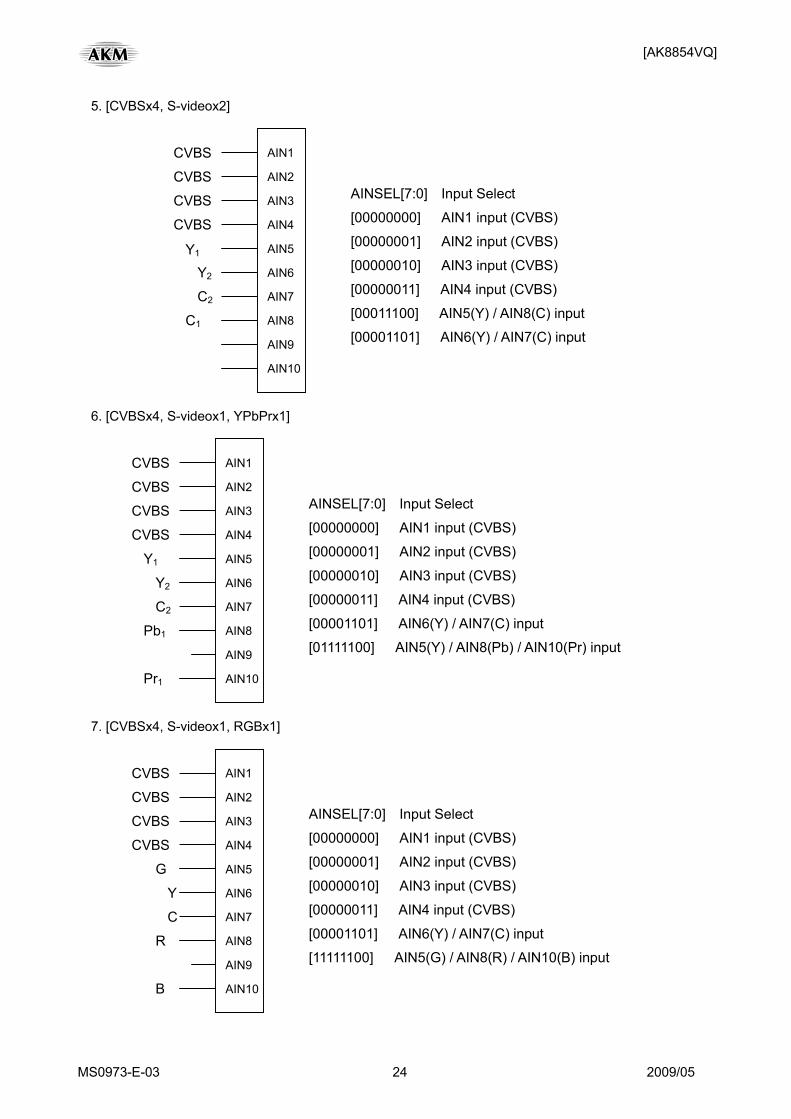
5. [CVBSx4, S-videox2]
Y2
CVBS
CVBS
CVBS
CVBS
C2
AIN1
AIN2
AIN3
AIN4
AIN5
AIN6
AIN7
AIN8
AIN9
AIN10
AINSEL[7:0] Input Select
[00000000] AIN1 input (CVBS)
[00000001] AIN2 input (CVBS)
[00000010] AIN3 input (CVBS)
[00000011] AIN4 input (CVBS)
[00011100] AIN5(Y) / AIN8(C) input
[00001101] AIN6(Y) / AIN7(C) input
Y1
C1
6. [CVBSx4, S-videox1, YPbPrx1]
Y2
CVBS
CVBS
CVBS
CVBS
C2
AIN1
AIN2
AIN3
AIN4
AIN5
AIN6
AIN7
AIN8
AIN9
AIN10
AINSEL[7:0] Input Select
[00000000] AIN1 input (CVBS)
[00000001] AIN2 input (CVBS)
[00000010] AIN3 input (CVBS)
[00000011] AIN4 input (CVBS)
[00001101] AIN6(Y) / AIN7(C) input
[01111100] AIN5(Y) / AIN8(Pb) / AIN10(Pr) input
Y1
Pb1
Pr1
7. [CVBSx4, S-videox1, RGBx1]
Y
CVBS
CVBS
CVBS
CVBS
C
AIN1
AIN2
AIN3
AIN4
AIN5
AIN6
AIN7
AIN8
AIN9
AIN10
AINSEL[7:0] Input Select
[00000000] AIN1 input (CVBS)
[00000001] AIN2 input (CVBS)
[00000010] AIN3 input (CVBS)
[00000011] AIN4 input (CVBS)
[00001101] AIN6(Y) / AIN7(C) input
[11111100] AIN5(G) / AIN8(R) / AIN10(B) input
G
R
B
[AK8854VQ]
MS0973-E-03 25 2009/05
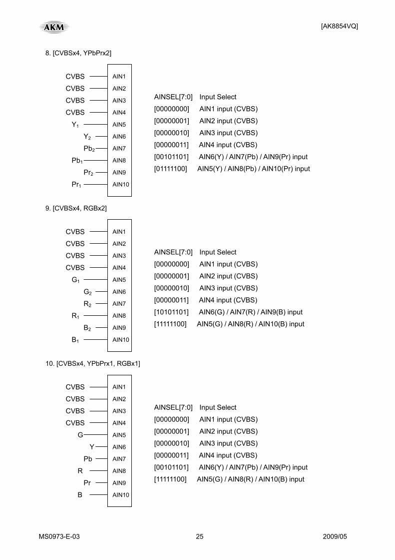
8. [CVBSx4, YPbPrx2]
Y2
CVBS
CVBS
CVBS
CVBS
Pb2
AIN1
AIN2
AIN3
AIN4
AIN5
AIN6
AIN7
AIN8
AIN9
AIN10
AINSEL[7:0] Input Select
[00000000] AIN1 input (CVBS)
[00000001] AIN2 input (CVBS)
[00000010] AIN3 input (CVBS)
[00000011] AIN4 input (CVBS)
[00101101] AIN6(Y) / AIN7(Pb) / AIN9(Pr) input
[01111100] AIN5(Y) / AIN8(Pb) / AIN10(Pr) input
Y1
Pb1
Pr1
Pr2
9. [CVBSx4, RGBx2]
G2
CVBS
CVBS
CVBS
CVBS
R2
AIN1
AIN2
AIN3
AIN4
AIN5
AIN6
AIN7
AIN8
AIN9
AIN10
AINSEL[7:0] Input Select
[00000000] AIN1 input (CVBS)
[00000001] AIN2 input (CVBS)
[00000010] AIN3 input (CVBS)
[00000011] AIN4 input (CVBS)
[10101101] AIN6(G) / AIN7(R) / AIN9(B) input
[11111100] AIN5(G) / AIN8(R) / AIN10(B) input
G1
R1
B1
B2
10. [CVBSx4, YPbPrx1, RGBx1]
Y
CVBS
CVBS
CVBS
CVBS
Pb
AIN1
AIN2
AIN3
AIN4
AIN5
AIN6
AIN7
AIN8
AIN9
AIN10
AINSEL[7:0] Input Select
[00000000] AIN1 input (CVBS)
[00000001] AIN2 input (CVBS)
[00000010] AIN3 input (CVBS)
[00000011] AIN4 input (CVBS)
[00101101] AIN6(Y) / AIN7(Pb) / AIN9(Pr) input
[11111100] AIN5(G) / AIN8(R) / AIN10(B) input
G
R
B
Pr
[AK8854VQ]
MS0973-E-03 26 2009/05
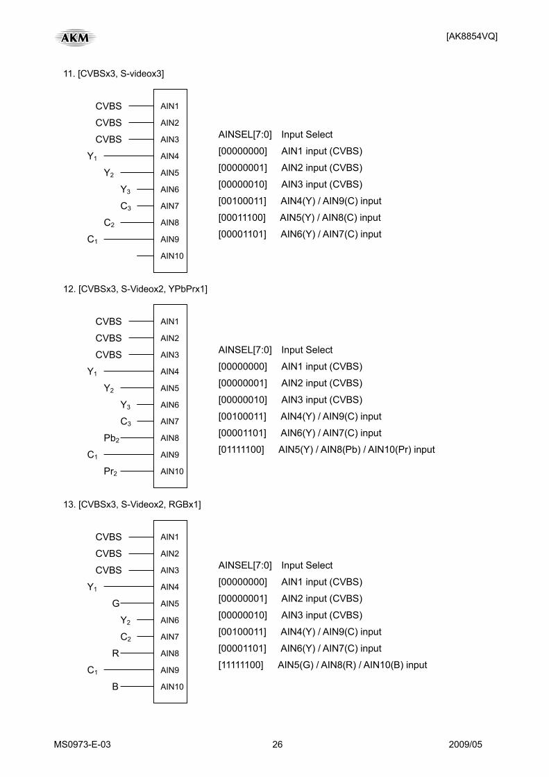
11. [CVBSx3, S-videox3]
Y3
CVBS
CVBS
CVBS
Y1
C3
AIN1
AIN2
AIN3
AIN4
AIN5
AIN6
AIN7
AIN8
AIN9
AIN10
AINSEL[7:0] Input Select
[00000000] AIN1 input (CVBS)
[00000001] AIN2 input (CVBS)
[00000010] AIN3 input (CVBS)
[00100011] AIN4(Y) / AIN9(C) input
[00011100] AIN5(Y) / AIN8(C) input
[00001101] AIN6(Y) / AIN7(C) input
Y2
C2
C1
12. [CVBSx3, S-Videox2, YPbPrx1]
Y3
CVBS
CVBS
CVBS
Y1
C3
AIN1
AIN2
AIN3
AIN4
AIN5
AIN6
AIN7
AIN8
AIN9
AIN10
AINSEL[7:0] Input Select
[00000000] AIN1 input (CVBS)
[00000001] AIN2 input (CVBS)
[00000010] AIN3 input (CVBS)
[00100011] AIN4(Y) / AIN9(C) input
[00001101] AIN6(Y) / AIN7(C) input
[01111100] AIN5(Y) / AIN8(Pb) / AIN10(Pr) input
Y2
Pb2
C1
Pr2
13. [CVBSx3, S-Videox2, RGBx1]
Y2
CVBS
CVBS
CVBS
Y1
C2
AIN1
AIN2
AIN3
AIN4
AIN5
AIN6
AIN7
AIN8
AIN9
AIN10
AINSEL[7:0] Input Select
[00000000] AIN1 input (CVBS)
[00000001] AIN2 input (CVBS)
[00000010] AIN3 input (CVBS)
[00100011] AIN4(Y) / AIN9(C) input
[00001101] AIN6(Y) / AIN7(C) input
[11111100] AIN5(G) / AIN8(R) / AIN10(B) input
G
R
C1
B
[AK8854VQ]
MS0973-E-03 27 2009/05
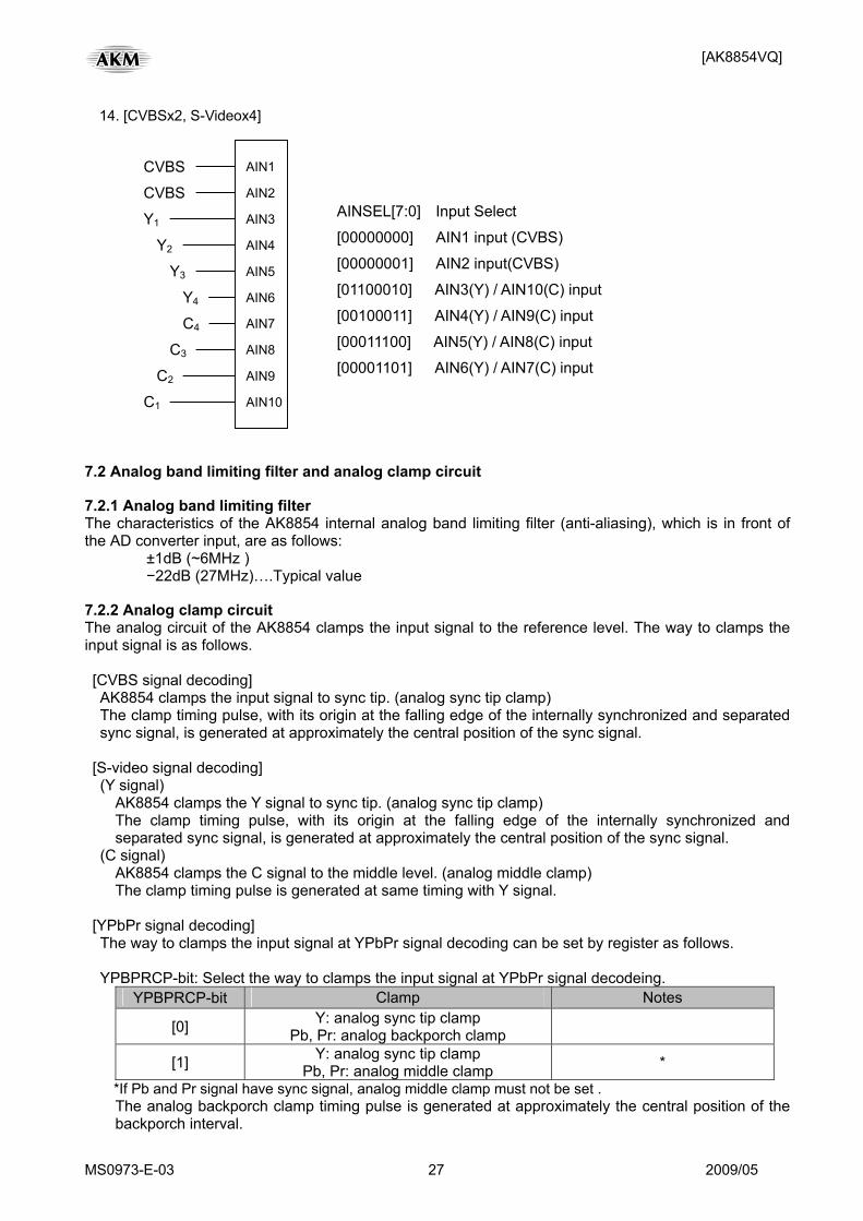
14. [CVBSx2, S-Videox4]
Y4
CVBS
CVBS
Y1
Y2
C4
AIN1
AIN2
AIN3
AIN4
AIN5
AIN6
AIN7
AIN8
AIN9
AIN10
AINSEL[7:0] Input Select
[00000000] AIN1 input (CVBS)
[00000001] AIN2 input(CVBS)
[01100010] AIN3(Y) / AIN10(C) input
[00100011] AIN4(Y) / AIN9(C) input
[00011100] AIN5(Y) / AIN8(C) input
[00001101] AIN6(Y) / AIN7(C) input
Y3
C3
C2
C1
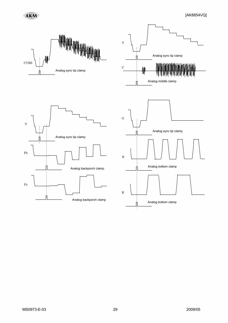
7.2 Analog band limiting filter and analog clamp circuit 7.2.1 Analog band limiting filter The characteristics of the AK8854 internal analog band limiting filter (anti-aliasing), which is in front of the AD converter input, are as follows: ±1dB (~6MHz ) −22dB (27MHz)….Typical value 7.2.2 Analog clamp circuit The analog circuit of the AK8854 clamps the input signal to the reference level. The way to clamps the input signal is as follows. [CVBS signal decoding] AK8854 clamps the input signal to sync tip. (analog sync tip clamp)
The clamp timing pulse, with its origin at the falling edge of the internally synchronized and separated sync signal, is generated at approximately the central position of the sync signal.
[S-video signal decoding] (Y signal) AK8854 clamps the Y signal to sync tip. (analog sync tip clamp)
The clamp timing pulse, with its origin at the falling edge of the internally synchronized and separated sync signal, is generated at approximately the central position of the sync signal.
(C signal) AK8854 clamps the C signal to the middle level. (analog middle clamp)
The clamp timing pulse is generated at same timing with Y signal. [YPbPr signal decoding] The way to clamps the input signal at YPbPr signal decoding can be set by register as follows.
YPBPRCP-bit: Select the way to clamps the input signal at YPbPr signal decodeing. YPBPRCP-bit Clamp Notes
[0] Y: analog sync tip clamp Pb, Pr: analog backporch clamp
[1] Y: analog sync tip clamp Pb, Pr: analog middle clamp *
*If Pb and Pr signal have sync signal, analog middle clamp must not be set . The analog backporch clamp timing pulse is generated at approximately the central position of the
backporch interval.
[AK8854VQ]
MS0973-E-03 28 2009/05
[RGB signal decoding] “Sync on Green” (G signal)
AK8854 clamps the G signal to sync tip. The clamp timing pulse, with its origin at the falling edge of the internally synchronized and
separated sync signal, is generated at approximately the central position of the sync signal. (B, R signal)
AK8854 clamps the B and R signal to the pedestal level. The clamp timing pulse is generated at same timing with G signal. (analog bottom clamp) But, if ALLSYNC is [1], AK8854 clamps all RGB signal to sync tip.
“H/VSYNC or CSYNC” AK8854 clamps all RGB signal to the pedestal level. The clamp timing pulse, with its origin at the
falling edge of the internally synchronized and separated sync signal, is generated at approximately the central position of the sync signal. (analog bottom clamp) But, if ALLSYNC is [1], AK8854 clamps all RGB signal to sync tip.
ALLSYNC-bit: Setting for sync signal of RGB input.
ALLSYNC-bit Sync signal of RGB Notes
[0] (SOG): R and B signals don’t contain sync signal. (C, H/V): All RGB signals don’t contain sync signal.
[1] (SOG): R and G signals also contain sync signal. (C, H/V): All RGB signals contain sync signal.
(SOG): Sync On Green (C,H/V): CSYNC or H/VSYNC
Pulse positions are bellow.
[AK8854VQ]
MS0973-E-03 29 2009/05
Analog middle clamp
Analog sync tip clamp
Y
CAnalog sync tip clamp
CVBS
Analog sync tip clamp
Y
Pb
Pr
Analog backporch clamp
Analog backporch clamp
Analog sync tip clamp
G
Analog bottom clamp
B
Analog bottom clamp
R
[AK8854VQ]
MS0973-E-03 30 2009/05
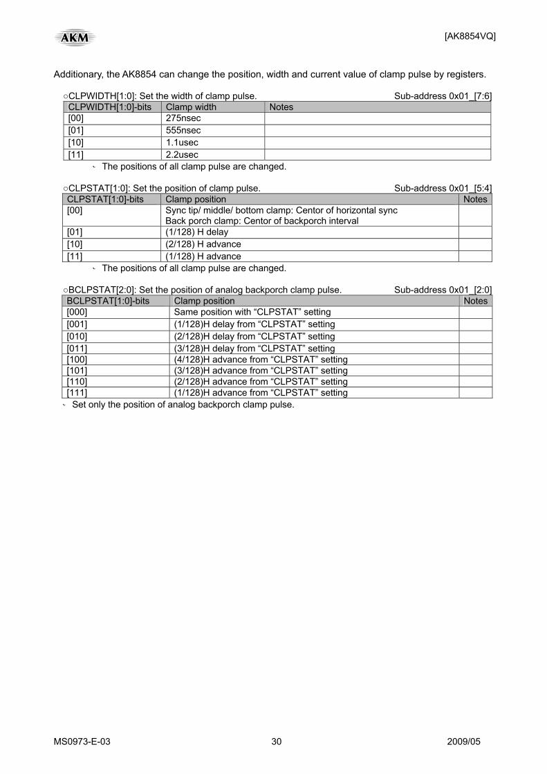
Additionary, the AK8854 can change the position, width and current value of clamp pulse by registers. CLPWIDTH[1:0]: Set the width of clamp pulse. Sub-address 0x01_[7:6]
CLPWIDTH[1:0]-bits Clamp width Notes [00] 275nsec [01] 555nsec [10] 1.1usec [11] 2.2usec
※The positions of all clamp pulse are changed. CLPSTAT[1:0]: Set the position of clamp pulse. Sub-address 0x01_[5:4] CLPSTAT[1:0]-bits Clamp position Notes[00] Sync tip/ middle/ bottom clamp: Centor of horizontal sync
Back porch clamp: Centor of backporch interval
[01] (1/128) H delay [10] (2/128) H advance [11] (1/128) H advance
※The positions of all clamp pulse are changed. BCLPSTAT[2:0]: Set the position of analog backporch clamp pulse. Sub-address 0x01_[2:0] BCLPSTAT[1:0]-bits Clamp position Notes[000] Same position with “CLPSTAT” setting [001] (1/128)H delay from “CLPSTAT” setting [010] (2/128)H delay from “CLPSTAT” setting [011] (3/128)H delay from “CLPSTAT” setting [100] (4/128)H advance from “CLPSTAT” setting [101] (3/128)H advance from “CLPSTAT” setting [110] (2/128)H advance from “CLPSTAT” setting [111] (1/128)H advance from “CLPSTAT” setting ※Set only the position of analog backporch clamp pulse.
[AK8854VQ]
MS0973-E-03 31 2009/05
CLPSTAT[1:0] = 00
CLPSTAT[1:0] = 01
CLPSTAT[1:0] = 11
CLPSTAT[1:0] = 10
Clamp Timing Pulse
CLPSTAT[1:0] = 00 BCLPSTAT[2:0] = 000
2/128H advance
CLPWIDTH[1:0]
CLPSTAT[1:0] =10 BCLPSTAT[2:0] = 000
3/128H advance CLPSTAT[1:0] =10 BCLPSTAT[2:0] = 111
2/128H advance CLPSTAT[1:0] =10 BCLPSTAT[2:0] = 000
2/128H advance
1/128H delay
1/128H advance
CLPWIDTH[1:0]
Sync tip/ middle/ bottom clamp
Back porch clamp
CLPG[1:0]: Set the current value of fine clamp in analog block. Sub-address 0x02_[1:0]
CLPG[1:0]-bit Clamp current value Notes [00] Min. [01] Middle 1 (Default) [10] Middle 2 [11] Max.
Middle 1 < Middle 2
UDG[1:0]:Set the current value of rough clamp in analog block. Sub-address 0x02_[3:2]
UDG[1:0]-bit Clamp current value Notes [00] Min. (Default) [01] Middle 1 [10] Middle 2 [11] Max.
Middle 1 < Middle 2
Its digital circuit clamps the digitized input data to the pedestal level (digital pedestal clamp), as described in Sec. 7.20 below.
[AK8854VQ]
MS0973-E-03 32 2009/05
7.3 Input video signal categorization [CVBS and S-video signal decoding] The AK8854 can decode the following video signals, in accordance with the register setting. NTSC-M,J NTSC-4.43 PAL-B,D,G,H,I,N PAL-Nc PAL-M PAL-60 SECAM In auto detection mode, it automatically recognizes the input signal category, from among the above. The register settings for the input signal characterization are essentially as follows. VSCF[1:0]-bits: Setting for subcarrier frequency of input signal.
VSCF[1:0]-bits Subcarrier frequency (MHz) Formats [00] 3.57954545 NTSC-M,J [01] 3.57561149 PAL-M [10] 3.58205625 PAL-Nc
[11] 4.43361875 PAL-B, D, G, H, I, N, NTSC-4.43, PAL-60, SECAM*
*For SECAM input signal, set VSCF[1:0] to [11]. VCEN[1:0]-bits: Setting for color encode format of input signal.
VCEN[1:0]-bits Color encode format Notes [00] NTSC [01] PAL [10] SECAM * [11] Reserved
*In case of YPbPr and RGB, SECAM is prohibited. VLF-bit: Setting for line frequency of each input frame.
VLF-bit Number of lines Notes [0] 525 NTSC-M, J, NTSC-4.43, PAL-M, PAL-60 [1] 625 PAL-B, D, G, H, I, N, Nc, SECAM
BW-bit: Setting for decoding of input signal as monochrome signal (monochrome mode)
BW-bit Signal type Notes [0] Not monochrome (monochrome mode OFF) [1] Decode as monochrome signal (monochrome mode ON)
In the monochrome mode at CVBS decoding, the input signal is treated as a monochrome signal, and all sampling data digitized the the AD converter passes through the luminance process and is processed as a luminance signal. Thus, with this bit ON, the signal input to the Y/C separation block is all output as luminance signal data to the luminance signal processing block. In the monochrome mode at S-video decoding, Y signal is only decoded. In the monochrome mode, the CbCr code is output as 0x80 (601 level data) regardless of the input.
[AK8854VQ]
MS0973-E-03 33 2009/05
SETUP-bit: Setting for presence or absence of input signal SETUP.
SETUP-bit SETUP presence/absence Notes [0] Setup absent – [1] Setup present 7.5IRE Setup
With the Setup present setting, the luminance and color signals are processed as follows: Luminance signal: Y=(Y-7.5)/0.925 Color signal: U=U/0.925, V=V/0.925 [YPbPr signal decoding] The AK8854 can decode the following video signals, in accordance with the register setting. 525i, 625i (EIA-770.1-A and EIA-770.2-A) VLF-bit: Setting for line frequency of each input frame.
VLF-bit Number of lines Notes [0] 525 [1] 625
BW-bit: Setting for decoding of input signal as monochrome signal (monochrome mode)
BW-bit Signal type Notes [0] Not monochrome (monochrome mode OFF) [1] Decode as monochrome signal (monochrome mode ON) *
*Y signal is only decoded. SETUP-bit: Setting for presence or absence of input signal SETUP.
SETUP-bit SETUP presence/absence Notes [0] Setup absent – [1] Setup present 7.5IRE Setup
With the Setup present setting, the luminance and color signals are processed as follows: Luminance signal: Y=(Y-7.5)/0.925 Color signal: U=U/0.925, V=V/0.925 CSSL-bit: Setting for sync level of Y signal.
CSSL-bit Sync level(mV) Notes [0] 300 EIA-770.2-A [1] 286 EIA-770.1-A
[RGB signal decoding] The AK8854 can decode the following video signals, in accordance with the register setting. 525i, 625i (SMPTE-253M) VLF-bit: Setting for line frequency of each input frame.
VLF-bit Number of lines Notes [0] 525 [1] 625
RGBSS[1:0]-bits: Selecting sync signal for RGB intput.
RGBSS-bits Sync signal Notes [00] Sync On Green [01] CSYNC [10] H/VSYNC [11] Reserved

[AK8854VQ]
MS0973-E-03 34 2009/05
BW-bit: Setting for decoding of input signal as monochrome signal (monochrome mode)
BW-bit Signal type Notes [0] Not monochrome (monochrome mode OFF) [1] Decode as monochrome signal (monochrome mode ON) *
*Y signal is only decoded. SETUP-bit: Setting for presence or absence of input signal SETUP.
SETUP-bit SETUP presence/absence Notes [0] Setup absent – [1] Setup present 7.5IRE Setup
With the Setup present setting, the luminance and color signals are processed as follows: Luminance signal: Y=(Y-7.5)/0.925 Color signal: U=U/0.925, V=V/0.925 ALLSYNC-bit: Setting for RGB signal with or without sync signal.]
ALLSYNC-bit Sync signal Notes
[0] (SOG): There is sync signal on Green only. (C. H/ V): There are not sync signals on all RGB.
[1] (SOG):There are sync signals on all RGB. (C. H/ V): There are sync signals on all RGB.
*
*(SOG): Sync On Green input (C, H/ V):CSYNC orH/VSYNC input CSSL-bit: Setting for sync level.
CSSL-bit Sync level(mV) Notes [0] 300 [1] 286
CSCL-bit: Setting for level of color transform.
CSCL-bit Transform level Notes [0] 700mV corresponding [1] 714mV corresponding
*There is relation between CSSL-bit and CSCL-bit.
CSSL-bit CSCL-bit [0] Input sync/ active signal is 300mV/ 700mV.
[0] [1] Input sync/ active signal is 300mV/ 700mV.
But, the active level of color transform is 714mV.
[0] Input sync/ active signal is 286mV/ 714mV. But, the active level of color transform is 700mV. [1]
[1] Input sync/ active signal is 286mV/ 714mV..
Ak8854 acceptH/VSYNC orCSYNC as external sync signal The register for H/VSYNC orCSYNC is as follows.
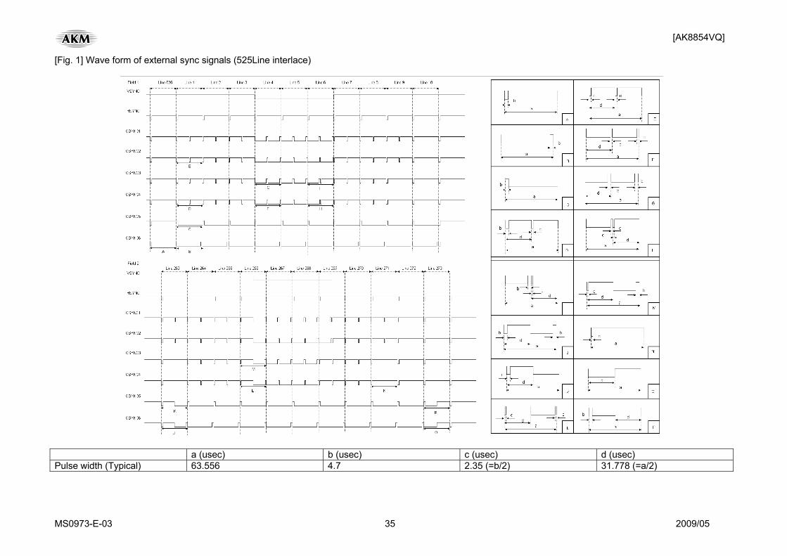
CSY[1:0]-bit: Setting for wave form of external sync signal.
CSY-bit Sync type Notes [00] CSYNC1 ~ 4 [01] CSYNC5H/VSYNC [10] CSYNC6 [11] Reserved
Refer to fig. 1 ~ 4.
[AK8854VQ]
MS0973-E-03 35 2009/05
[Fig. 1] Wave form of external sync signals (525Line interlace)
a (usec) b (usec) c (usec) d (usec) Pulse width (Typical) 63.556 4.7 2.35 (=b/2) 31.778 (=a/2)
[AK8854VQ]
MS0973-E-03 36 2009/05
[Fig. 2] Wave form of external sync signals (625Line interlace)
a (usec) b (usec) c (usec) d (usec) Pulse width (Typical) 64 4.7 2.35 (=b/2) 32 (=a/2)
[AK8854VQ]
MS0973-E-03 37 2009/05
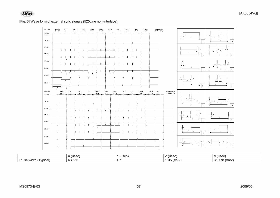
[Fig. 3] Wave form of external sync signals (525Line non-interlace)
a (usec) b (usec) c (usec) d (usec) Pulse width (Typical) 63.556 4.7 2.35 (=b/2) 31.778 (=a/2)
[AK8854VQ]
MS0973-E-03 38 2009/05
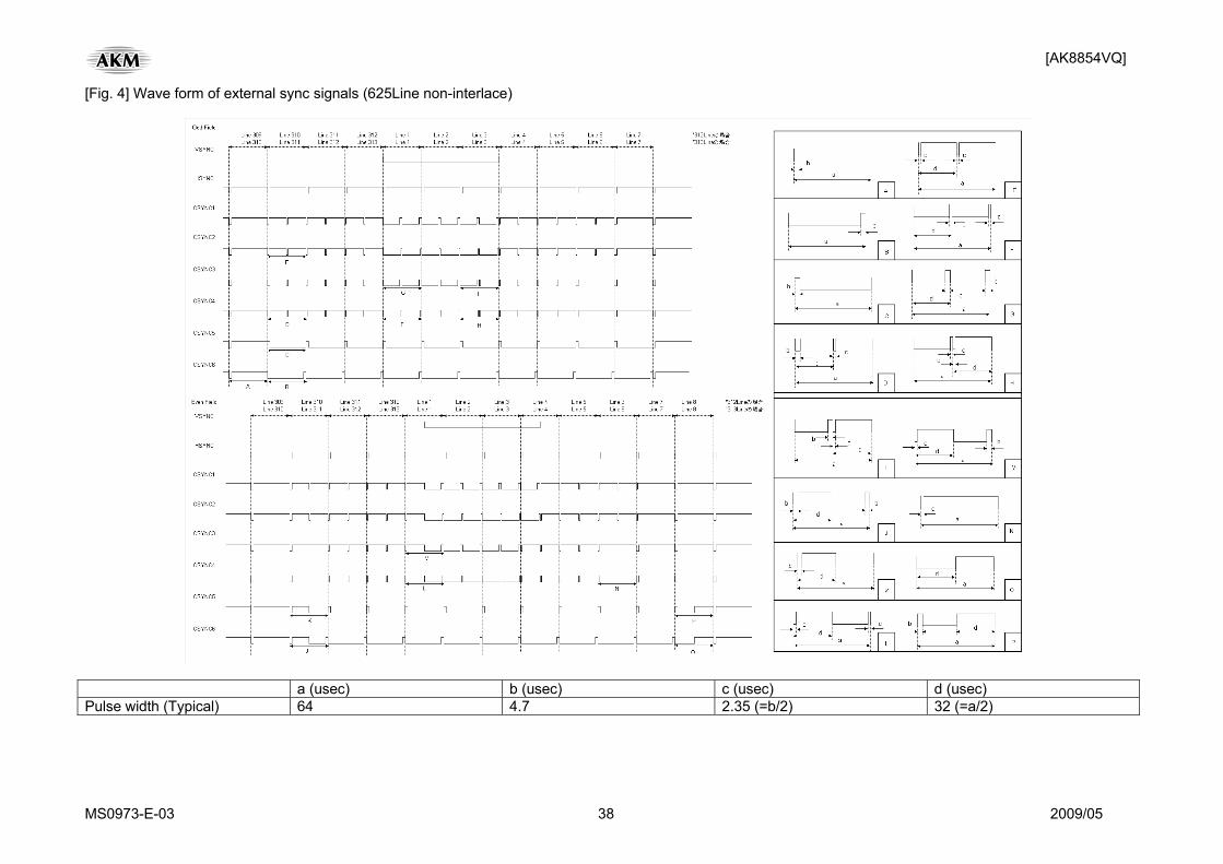
[Fig. 4] Wave form of external sync signals (625Line non-interlace)
a (usec) b (usec) c (usec) d (usec) Pulse width (Typical) 64 4.7 2.35 (=b/2) 32 (=a/2)
[AK8854VQ]
MS0973-E-03 39 2009/05
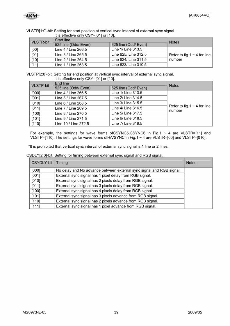
VLSTR[1:0]-bit: Setting for start position at vertical sync interval of external sync signal.
It is effective only CSY=[01] or [10]. Start line VLSTR-bit 525 line (Odd/ Even) 625 line (Odd/ Even) Notes
[00] Line 4 / Line 266.5 Line 1/ Line 313.5 [01] Line 3 / Line 265.5 Line 625/ Line 312.5 [10] Line 2 / Line 264.5 Line 624/ Line 311.5 [11] Line 1 / Line 263.5 Line 623/ Line 310.5
Refer to fig.1 ~ 4 for line number
VLSTP[2:0]-bit: Setting for end position at vertical sync interval of external sync signal.
It is effective only CSY=[01] or [10]. End line VLSTP-bit 525 line (Odd/ Even) 625 line (Odd/ Even) Notes
[000] Line 4 / Line 266.5 Line 1/ Line 313.5 [001] Line 5 / Line 267.5 Line 2/ Line 314.5 [010] Line 6 / Line 268.5 Line 3/ Line 315.5 [011] Line 7 / Line 269.5 Line 4/ Line 316.5 [100] Line 8 / Line 270.5 Line 5/ Line 317.5 [101] Line 9 / Line 271.5 Line 6/ Line 318.5 [110] Line 10 / Line 272.5 Line 7/ Line 319.5
Refer to fig.1 ~ 4 for line number
For example, the settings for wave forms ofCSYNC5,CSYNC6 in Fig.1 ~ 4 are VLSTR=[11] and
VLSTP=[110]. The settings for wave forms ofH/VSYNC in Fig.1 ~ 4 are VLSTR=[00] and VLSTP=[010]. *It is prohibited that vertical sync interval of external sync signal is 1 line or 2 lines.
CSDLY[2:0]-bit: Setting for timing between external sync signal and RGB signal.
CSYDLY-bit Timing Notes
[000] No delay and No advance between external sync signal and RGB signal [001] External sync signal has 1 pixel delay from RGB signal. [010] External sync signal has 2 pixels delay from RGB signal. [011] External sync signal has 3 pixels delay from RGB signal. [100] External sync signal has 4 pixels delay from RGB signal. [101] External sync signal has 3 pixels advance from RGB signal. [110] External sync signal has 2 pixels advance from RGB signal. [111] External sync signal has 1 pixel advance from RGB signal.
[AK8854VQ]
MS0973-E-03 40 2009/05
The register settings for auto detection are essentially as follows. AUTODET-bit: Settings for auto detection of input signal (auto detection mode)
AUTODET-bit Auto detection Notes [0] OFF Manual setting [1] ON –
The auto detection recognizes the following parameters. Number of lines per frame: 525/625 Carrier frequencies: 3.57954545 3.57561149 3.58205625 4.43361875 Color encoding formats: NTSC PAL SECAM Monochrome signal: Not monochrome/monochrome
Note: Automatic monochrome detection is active if the color kill setting is ON (COLKILL-bit = [1].) The AK8854 stores the detected parameter to the Input Video Status Register (thus, as an internal notice function). This enables the host to distinguish among the formats NTSC-M, J; NTSC-4.43; PAL-B, D, G, H, I, N; PAL-M; PAL-Nc; PAL-60; SECAM; and monochrome. It should be noted that it does not detect NTSC-M, NTSC-J, or PAL-B, D, G, H, I, N formats. And, AK8854 can detect only 525L/ 625L at YPbPr or RGB input. In auto detection, the candidates for detection can be limited as shown below. NDMODE Register: For limiting auto detection candidates
Bit Register Name R/W Definition
bit 0 NDPALM No Detect PAL-M bit R/W [0]: PAL-M candidate [1]: PAL-M non-candidate
bit 1 NDPALNC No Detect PAL-Nc bit R/W [0]: PAL-Nc candidate [1]: PAL-Nc non-candidate
bit 2 NDSECAM No Detect SECAM bit R/W [0]: SECAM candidate [1]: SECAM non-candidate
bit 3 Reserved Reserved R/W Reserved
bit 4 NDNTSC443 No Detect NTSC-4.43 bit R/W [0]: NTSC-4.43 candidate [1]: NTSC-4.43 non-candidate
bit 5 NDPAL60 No Detect PAL-60 bit R/W [0]: PAL-60 candidate [1]: PAL-60 non-candidate
bit 6 ND525L No Detect 525Line bit R/W [0]: 525 line candidate [1]: 525 line non-candidate
bit 7 ND625L No Detect 625Line bit R/W [0]: 625 line candidate [1]: 625 line non-candidate
[AK8854VQ]
MS0973-E-03 41 2009/05
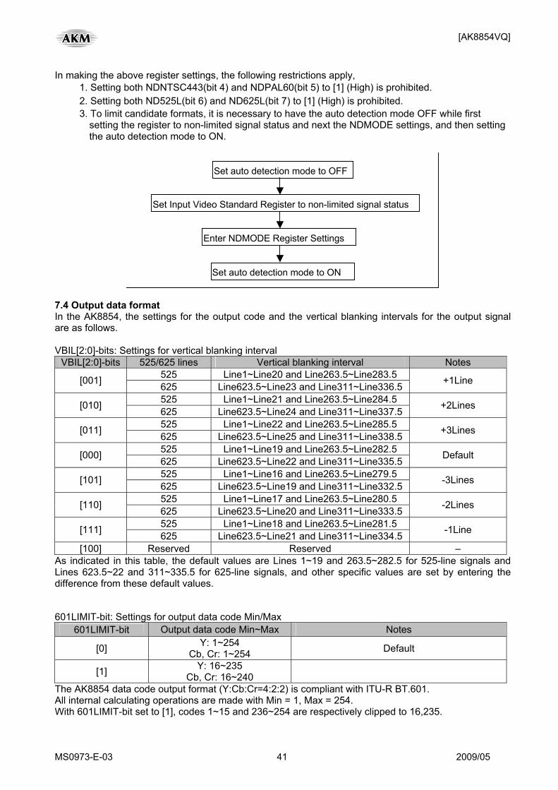
In making the above register settings, the following restrictions apply, 1. Setting both NDNTSC443(bit 4) and NDPAL60(bit 5) to [1] (High) is prohibited. 2. Setting both ND525L(bit 6) and ND625L(bit 7) to [1] (High) is prohibited. 3. To limit candidate formats, it is necessary to have the auto detection mode OFF while first setting the register to non-limited signal status and next the NDMODE settings, and then setting the auto detection mode to ON.
Set auto detection mode to OFF
Set Input Video Standard Register to non-limited signal status
Enter NDMODE Register Settings
Set auto detection mode to ON
7.4 Output data format In the AK8854, the settings for the output code and the vertical blanking intervals for the output signal are as follows. VBIL[2:0]-bits: Settings for vertical blanking interval
VBIL[2:0]-bits 525/625 lines Vertical blanking interval Notes 525 Line1~Line20 and Line263.5~Line283.5 [001] 625 Line623.5~Line23 and Line311~Line336.5 +1Line
525 Line1~Line21 and Line263.5~Line284.5 [010] 625 Line623.5~Line24 and Line311~Line337.5 +2Lines
525 Line1~Line22 and Line263.5~Line285.5 [011] 625 Line623.5~Line25 and Line311~Line338.5 +3Lines
525 Line1~Line19 and Line263.5~Line282.5 [000] 625 Line623.5~Line22 and Line311~Line335.5 Default
525 Line1~Line16 and Line263.5~Line279.5 [101] 625 Line623.5~Line19 and Line311~Line332.5 -3Lines
525 Line1~Line17 and Line263.5~Line280.5 [110] 625 Line623.5~Line20 and Line311~Line333.5 -2Lines
525 Line1~Line18 and Line263.5~Line281.5 [111] 625 Line623.5~Line21 and Line311~Line334.5 -1Line
[100] Reserved Reserved – As indicated in this table, the default values are Lines 1~19 and 263.5~282.5 for 525-line signals and Lines 623.5~22 and 311~335.5 for 625-line signals, and other specific values are set by entering the difference from these default values. 601LIMIT-bit: Settings for output data code Min/Max
601LIMIT-bit Output data code Min~Max Notes
[0] Y: 1~254 Cb, Cr: 1~254 Default
[1] Y: 16~235 Cb, Cr: 16~240
The AK8854 data code output format (Y:Cb:Cr=4:2:2) is compliant with ITU-R BT.601. All internal calculating operations are made with Min = 1, Max = 254. With 601LIMIT-bit set to [1], codes 1~15 and 236~254 are respectively clipped to 16,235.
[AK8854VQ]
MS0973-E-03 42 2009/05
TRSVSEL-bit: Settings for V-bit handling in ITU-R BT.656 format
525-line 625-line TRSVSEL-bit V-bit=0 V-bit=1 V-bit=0 V-bit=1
[0] ITU-R BT 656-3
compliant
Line10~Line263 Line273~Line525
Line1~Line9 Line264~Line272
[1] ITU-R BT 656-4 SMPTE125M
compliant
Line20~Line263 Line283~Line525
Line1~Line19 Line264~Line282
Line23~Line310 Line336~Line623
Line1~Line22 Line311~Line335Line624~Line625
These values are unaffected by the VBIL[2:0]-bits setting. SLLVL-bit: Settings for slice level SLLVL-bit Slice level [0] 25IRE [1] 50IRE
The results of VBI slicing by the AK8854 slicing function are output as ITU-R BT.601 digital data. The VBI interval is set via VBIL[2:0]-bits. VBI slicing is performed in the luminance signal processing path, so that the Cb/Cr value of the effective line 601 output code is output at the same level as the corresponding luminance signal. The slice level and the output code are set via the register. The output code value is set via the Hi/Low Slice Data Set Register, as follows.
Hi Slice Data Set Register*: Setting for higher of two values resulting from slicing. Default: 0xEB(235)
Low Slice Data Set Register*: Setting for lower of two values resulting from slicing. Default: 0x10(16)
*Note that a setting of 0x00 or 0xFF corresponds to a special 601 code. VBIDEC[1:0]-bits: Settings for decode data in the VBI period
VBIDEC[1:0]-bits Decode data Notes
[00] Black level output Y = 0x10 Cb/Cr = 0x80
[01] Monochrome mode Y = data converted to 601 level Cb/Cr = 0x80
[10] Sliced data output during VBI Y/Cb/Cr = value corresponding to slice level (Value set at Hi/Low Slice Data Set Register)
[11] Reserved Reserved Note that, with VBI period settings of Lines 1~9 and 263.5~272.5 in the 525 Line and Lines 623.5~6.5 and 311~318 in the 625 Line, the setting VBIDEC[1:0] will not be entered and the output will be in Black level code.
[AK8854VQ]
MS0973-E-03 43 2009/05
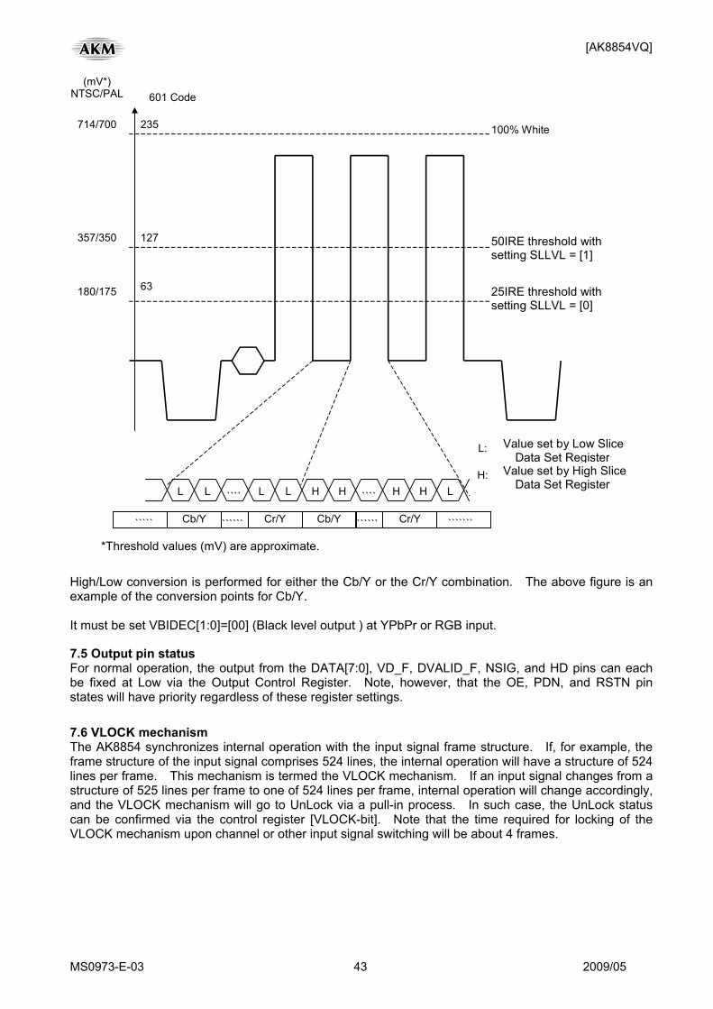
(mV*) NTSC/PAL 601 Code
714/700 235
357/350
180/175
*Threshold values (mV) are approximate.
127
63
100% White
50IRE threshold with setting SLLVL = [1]
25IRE threshold with setting SLLVL = [0]
```` LL L ```` L L H H H H
Cb/Y Cr/Y `````` Cb/Y `````` Cr/Y
L:
H: Value set by High Slice Data Set Register
Value set by Low Slice Data Set Register
````` ```````
High/Low conversion is performed for either the Cb/Y or the Cr/Y combination. The above figure is an example of the conversion points for Cb/Y. It must be set VBIDEC[1:0]=[00] (Black level output ) at YPbPr or RGB input. 7.5 Output pin status For normal operation, the output from the DATA[7:0], VD_F, DVALID_F, NSIG, and HD pins can each be fixed at Low via the Output Control Register. Note, however, that the OE, PDN, and RSTN pin states will have priority regardless of these register settings.
7.6 VLOCK mechanism The AK8854 synchronizes internal operation with the input signal frame structure. If, for example, the frame structure of the input signal comprises 524 lines, the internal operation will have a structure of 524 lines per frame. This mechanism is termed the VLOCK mechanism. If an input signal changes from a structure of 525 lines per frame to one of 524 lines per frame, internal operation will change accordingly, and the VLOCK mechanism will go to UnLock via a pull-in process. In such case, the UnLock status can be confirmed via the control register [VLOCK-bit]. Note that the time required for locking of the VLOCK mechanism upon channel or other input signal switching will be about 4 frames.
[AK8854VQ]
MS0973-E-03 44 2009/05
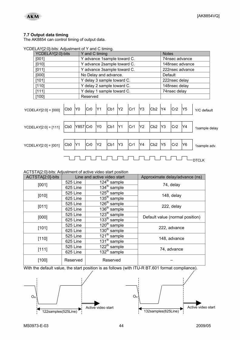
7.7 Output data timing The AK8854 can control timing of output data. YCDELAY[2:0]-bits: Adjustment of Y and C timing.
YCDELAY[2:0]-bits Y and C timing Notes [001] Y advance 1sample toward C. 74nsec advance [010] Y advance 2sample toward C. 148nsec advance [011] Y advance 3sample toward C. 222nsec advance [000] No Delay and advance. Default [101] Y delay 3 sample toward C. 222nsec delay [110] Y delay 2 sample toward C. 148nsec delay [111] Y delay 1 sample toward C. 74nsec delay [100] Reserved
DTCLK
Cb0 Y0 Cr0 Y1 Cb1 Y2 Cr1 Y3 Cb2 Y4 Cr2 Y5
Cb0 Y857 Cr0 Y0 Cb1 Y1 Cr1 Y2 Cb2 Y3 Cr2 Y4
Cb0 Y1 Cr0 Y2 Cb1 Y3 Cr1 Y4 Cb2 Y5 Cr2 Y6 YCDELAY[2:0] = [001]
YCDELAY[2:0] = [111]
Y/C default
1sample delay
1sample adv.
YCDELAY[2:0] = [000]
ACTSTA[2:0]-bits: Adjustment of active video start position
ACTSTA[2:0]-bits Line and active video start Approximate delay/advance (ns)525 Line 124th sample [001] 625 Line 134th sample
74, delay
525 Line 125th sample [010] 625 Line 135th sample
148, delay
525 Line 126th sample [011] 625 Line 136th sample 222, delay
525 Line 123th sample [000] 625 Line 133th sample Default value (normal position)
525 Line 120th sample [101] 625 Line 130th sample 222, advance
525 Line 121th sample [110] 625 Line 131th sample 148, advance
525 Line 122th sample [111] 625 Line 132th sample 74, advance
[100] Reserved Reserved –
With the default value, the start position is as follows (with ITU-R BT.601 format compliance).
122samples(525Line) Active video start
OH
132samples(625Line) Active video start
OH
[AK8854VQ]
MS0973-E-03 45 2009/05
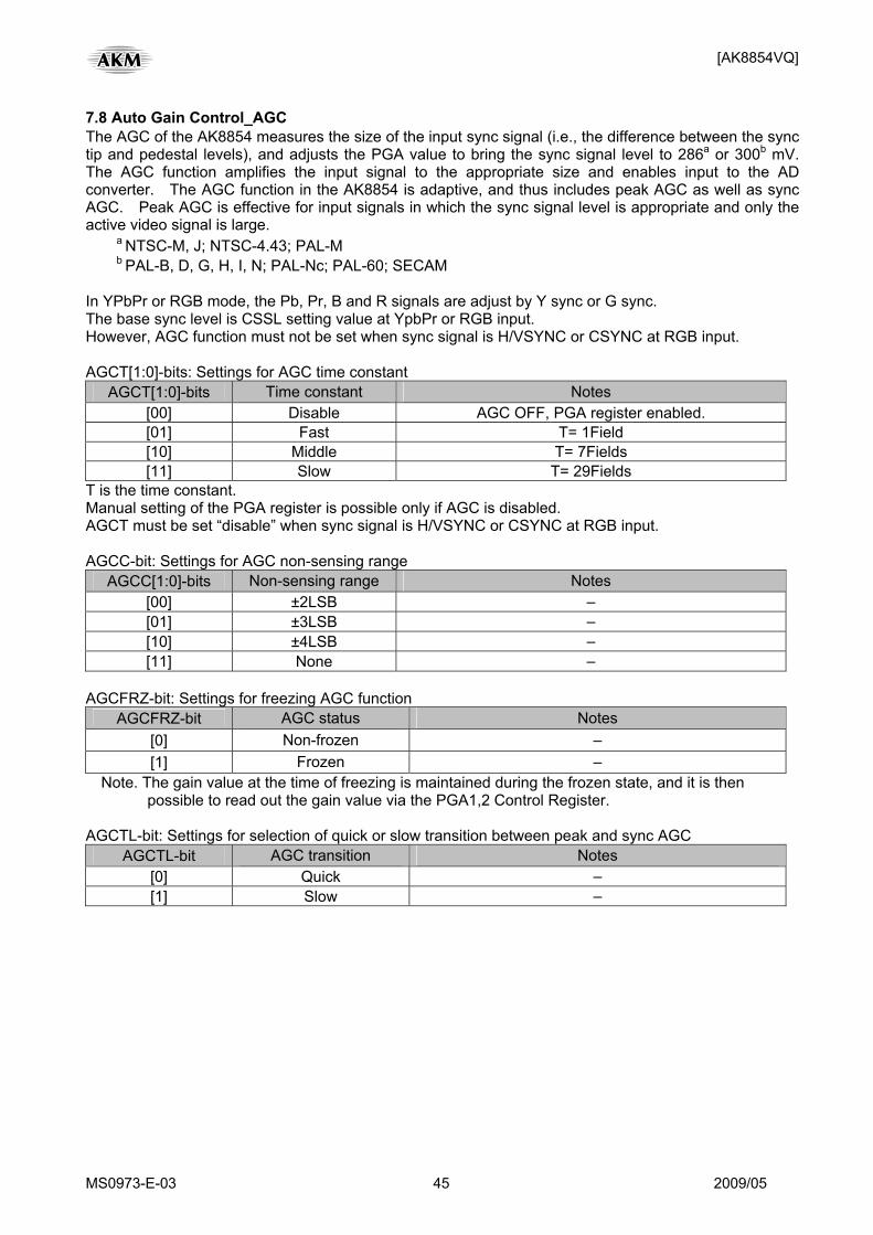
7.8 Auto Gain Control_AGC The AGC of the AK8854 measures the size of the input sync signal (i.e., the difference between the sync tip and pedestal levels), and adjusts the PGA value to bring the sync signal level to 286a or 300b mV. The AGC function amplifies the input signal to the appropriate size and enables input to the AD converter. The AGC function in the AK8854 is adaptive, and thus includes peak AGC as well as sync AGC. Peak AGC is effective for input signals in which the sync signal level is appropriate and only the active video signal is large.
a NTSC-M, J; NTSC-4.43; PAL-M b PAL-B, D, G, H, I, N; PAL-Nc; PAL-60; SECAM In YPbPr or RGB mode, the Pb, Pr, B and R signals are adjust by Y sync or G sync. The base sync level is CSSL setting value at YpbPr or RGB input. However, AGC function must not be set when sync signal is H/VSYNC or CSYNC at RGB input. AGCT[1:0]-bits: Settings for AGC time constant
AGCT[1:0]-bits Time constant Notes [00] Disable AGC OFF, PGA register enabled. [01] Fast T= 1Field [10] Middle T= 7Fields [11] Slow T= 29Fields
T is the time constant. Manual setting of the PGA register is possible only if AGC is disabled. AGCT must be set “disable” when sync signal is H/VSYNC or CSYNC at RGB input. AGCC-bit: Settings for AGC non-sensing range
AGCC[1:0]-bits Non-sensing range Notes [00] ±2LSB – [01] ±3LSB – [10] ±4LSB – [11] None –
AGCFRZ-bit: Settings for freezing AGC function
AGCFRZ-bit AGC status Notes [0] Non-frozen – [1] Frozen –
Note. The gain value at the time of freezing is maintained during the frozen state, and it is then possible to read out the gain value via the PGA1,2 Control Register.
AGCTL-bit: Settings for selection of quick or slow transition between peak and sync AGC
AGCTL-bit AGC transition Notes [0] Quick – [1] Slow –
[AK8854VQ]
MS0973-E-03 46 2009/05
7.9 Auto Color Control_ACC The ACC of the AK8854 measures the level of the input signal color burst, and adjusts the level to 286a or 300b mV, as appropriate. The ACC is not applicable to SECAM, YPbPr and RGB input. As in AGC, both ACC time constant and ACC freeze settings can be entered. a NTSC-M,J, NTSC-4.43, PAL-M b PAL-B, D, G, H, I, N, PAL-Nc, PAL-60 ACCT[1:0]-bits: Settings for ACC time constant
ACCT[1:0]-bits Time constant Notes [00] Disable ACC OFF [01] Fast T= 2Fields [10] Middle T= 8Fields [11] Slow T= 30Fields
ACCFRZ-bit: Settings for freezing ACC function
ACCFRZ-bit ACC status Notes [0] Non-frozen – [1] Frozen –
Note. The burst-level setting at the time of freezing is maintained during the frozen state. The ACC and Color saturation functions operate independently. If ACC is enabled, the color saturation adjustment is applied to the signal that has been adjusted to the appropriate level by the ACC. 7.10 Y/C separation The adaptive two-dimensional Y/C separation of the AK8854 utilizes a correlation detector to select the best-correlated direction from among vertical, horizontal, and diagonal samples, and selects the optimum Y/C separation mode. For NTSC-4.43, PAL-60, and SECAM inputs, the Y/C separation is one-dimensional only, regardless of the setting. YCSEP[1:0]-bits: Settings for Y/C separation method
YCSEP[1:0]-bits Y/C separation mode Notes [00] Adaptive Selects [01] or [10] setting, as appropriate [01] 1-D 1D (BPF)
[10] 2-D NTSC-M, J, PAL-M: 3 Line 2-D PAL-B, D, G, H, I, N, Nc: 5 Line 2-D
[11] Reserved — For NTSC-4.43, PAL-60, and SECAM inputs, Y/C separation is 1-D only, regardless of the setting. 7.11 C filter The bandwidth of the C filter can be set via the register, as follows. C358FIL[1:0]: Settings for C filter bandwidth, for input signal with 3.58 MHz subcarrier wave
C358FIL[1:0] -bits Notes Notes [00] Narrow [01] Medium [10] Wide [11] Reserved
NTSC-M, J, PAL-M, PAL-Nc
C443FIL[1:0]: Settings for C filter bandwidth, for input signal with 4.43 MHz subcarrier wave
C443FIL[1:0] -bits Notes Notes [00] Narrow [01] Medium [10] Wide [11] Reserved
PAL-B, D, G, H, I, N, NTSC-4.43, PAL-60
Note. No bandwidth selection is possible for SECAM input.
[AK8854VQ]
MS0973-E-03 47 2009/05
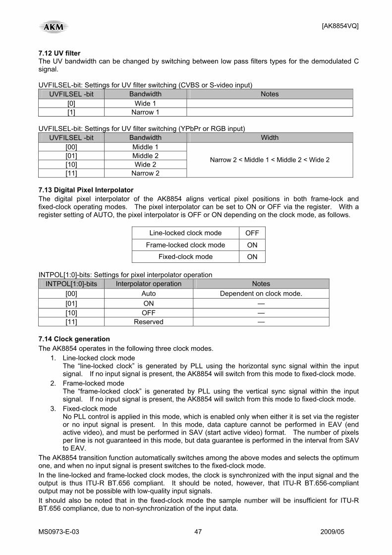
7.12 UV filter The UV bandwidth can be changed by switching between low pass filters types for the demodulated C signal. UVFILSEL-bit: Settings for UV filter switching (CVBS or S-video input)
UVFILSEL -bit Bandwidth Notes [0] Wide 1 [1] Narrow 1
UVFILSEL-bit: Settings for UV filter switching (YPbPr or RGB input)
UVFILSEL -bit Bandwidth Width [00] Middle 1 [01] Middle 2 [10] Wide 2 [11] Narrow 2
Narrow 2 < Middle 1 < Middle 2 < Wide 2
7.13 Digital Pixel Interpolator The digital pixel interpolator of the AK8854 aligns vertical pixel positions in both frame-lock and fixed-clock operating modes. The pixel interpolator can be set to ON or OFF via the register. With a register setting of AUTO, the pixel interpolator is OFF or ON depending on the clock mode, as follows.
Line-locked clock mode OFF
Frame-locked clock mode ON Fixed-clock mode ON
INTPOL[1:0]-bits: Settings for pixel interpolator operation
INTPOL[1:0]-bits Interpolator operation Notes [00] Auto Dependent on clock mode. [01] ON — [10] OFF — [11] Reserved —
7.14 Clock generation The AK8854 operates in the following three clock modes.
1. Line-locked clock mode The “line-locked clock” is generated by PLL using the horizontal sync signal within the input signal. If no input signal is present, the AK8854 will switch from this mode to fixed-clock mode.
2. Frame-locked mode The “frame-locked clock” is generated by PLL using the vertical sync signal within the input signal. If no input signal is present, the AK8854 will switch from this mode to fixed-clock mode.
3. Fixed-clock mode No PLL control is applied in this mode, which is enabled only when either it is set via the register or no input signal is present. In this mode, data capture cannot be performed in EAV (end active video), and must be performed in SAV (start active video) format. The number of pixels per line is not guaranteed in this mode, but data guarantee is performed in the interval from SAV to EAV.
The AK8854 transition function automatically switches among the above modes and selects the optimum one, and when no input signal is present switches to the fixed-clock mode. In the line-locked and frame-locked clock modes, the clock is synchronized with the input signal and the output is thus ITU-R BT.656 compliant. It should be noted, however, that ITU-R BT.656-compliant output may not be possible with low-quality input signals. It should also be noted that in the fixed-clock mode the sample number will be insufficient for ITU-R BT.656 compliance, due to non-synchronization of the input data.
[AK8854VQ]
MS0973-E-03 48 2009/05
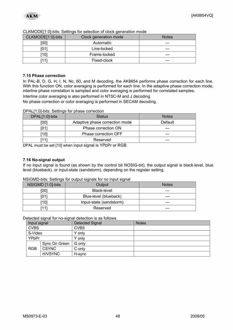
CLKMODE[1:0]-bits: Settings for selection of clock generation mode
CLKMODE[1:0]-bits Clock generation mode Notes [00] Automatic — [01] Line-locked — [10] Frame-locked — [11] Fixed-clock —
7.15 Phase correction In PAL-B, D, G, H, I, N, Nc, 60, and M decoding, the AK8854 performs phase correction for each line. With this function ON, color averaging is performed for each line. In the adaptive phase correction mode, interline phase correlation is sampled and color averaging is performed for correlated samples. Interline color averaging is also performed in NTSC-M and J decoding. No phase correction or color averaging is performed in SECAM decoding. DPAL[1:0]-bits: Settings for phase correction
DPAL[1:0]-bits Status Notes [00] Adaptive phase correction mode Default [01] Phase correction ON — [10] Phase correction OFF — [11] Reserved —
DPAL must be set [10] when input signal is YPbPr or RGB. 7.16 No-signal output If no input signal is found (as shown by the control bit NOSIG-bit), the output signal is black-level, blue level (blueback), or input-state (sandstorm), depending on the register setting. NSIGMD-bits: Settings for output signals for no input signal
NSIGMD [1:0]-bits Output Notes [00] Black-level — [01] Blue-level (blueback) — [10] Input-state (sandstorm) — [11] Reserved —
Detected signal for no-signal detection is as follows.
Input signal Detected Signal Notes CVBS CVBS S-Video Y only YPbPr Y only
Sync On Green G only CSYNC C only RGB H/VSYNC H-sync
[AK8854VQ]
MS0973-E-03 49 2009/05
7.17 Output interface 7.17.1 656 interface 7.17.1.1 Line-locked and frame-locked clock modes In both of these modes, the decoded data output is compliant with ITU-R BT.656, which requires the following sample and line numbers. Samples per line: 858 (525 line) or 864 (625 line) Lines per frame: 525 or 625 It may not be possible, however, to meet these requirements if the input signal quality is poor. In the AK8854, PLL is locked to the input signal and output-stage buffers absorb input signal jitter, but if the jitter is excessive PLL tracking may be impracticable and ITU-R BT.656 compliance may thus be lost. In such cases, the following processing can be applied via the indicated register settings.
(a) Line drop/repeat processing A line drop or line repeat will result in output signals with 524/624 or 526/626 lines per frame, respectively. Line drop/repeat processing may be performed at any line in the frame.
(b) Pixel drop/repeat processing A pixel drop or pixel repeat will result in output signals less or more than the required 858/864 samples in the last line of the frameor field, respectively. Note: In the event of output-stage buffer failure, line drop/repeat processing will be performed even if the register setting is for pixel drop/repeat processing.
ERRHND-bits: Settings for line and pixel drop/repeat processing
ERRHND-bits Processing mode Notes [00] Line Drop / Line Repeat Default [01] Pixel Drop / Pixel Repeat by Field — [10] Pixel Drop / Pixel Repeat by Frame — [11] Reserved —
[AK8854VQ]
MS0973-E-03 50 2009/05
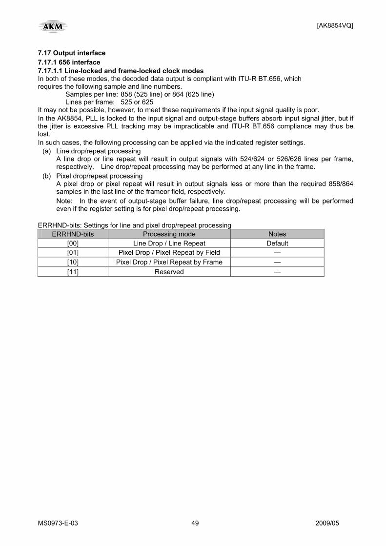
7.17.1.2 Fixed-clock mode In fixed-clock mode, operation is at an internally generated 27 MHz clock, from a 24.576 MHz input clock. The output signal is therefore not synchronized with the input signal, and thus not ITU- BT.656 compliant. Data is output in SAV format. As shown in the following figure, EAV is guaranteed for 720 pixels from SAV, but the sample number from EAV to SAV is not.
858 / 864 ( NTSC / PAL ) pixels ± α
SAV EAV
720 pixels
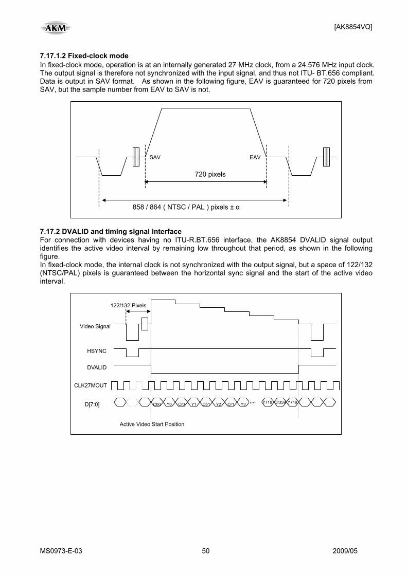
7.17.2 DVALID and timing signal interface For connection with devices having no ITU-R.BT.656 interface, the AK8854 DVALID signal output identifies the active video interval by remaining low throughout that period, as shown in the following figure. In fixed-clock mode, the internal clock is not synchronized with the output signal, but a space of 122/132 (NTSC/PAL) pixels is guaranteed between the horizontal sync signal and the start of the active video interval.
Video Signal
HSYNC
DVALID
CLK27MOUT
Cb0 Cr0Y0 Y1 Cb1 Y2 Cr1 Y3 Y719 Cr359Y718D[7:0]
Active Video Start Position
( 通 常 点 か ら
‘’’’
122/132 Pixels
[AK8854VQ]
MS0973-E-03 51 2009/05
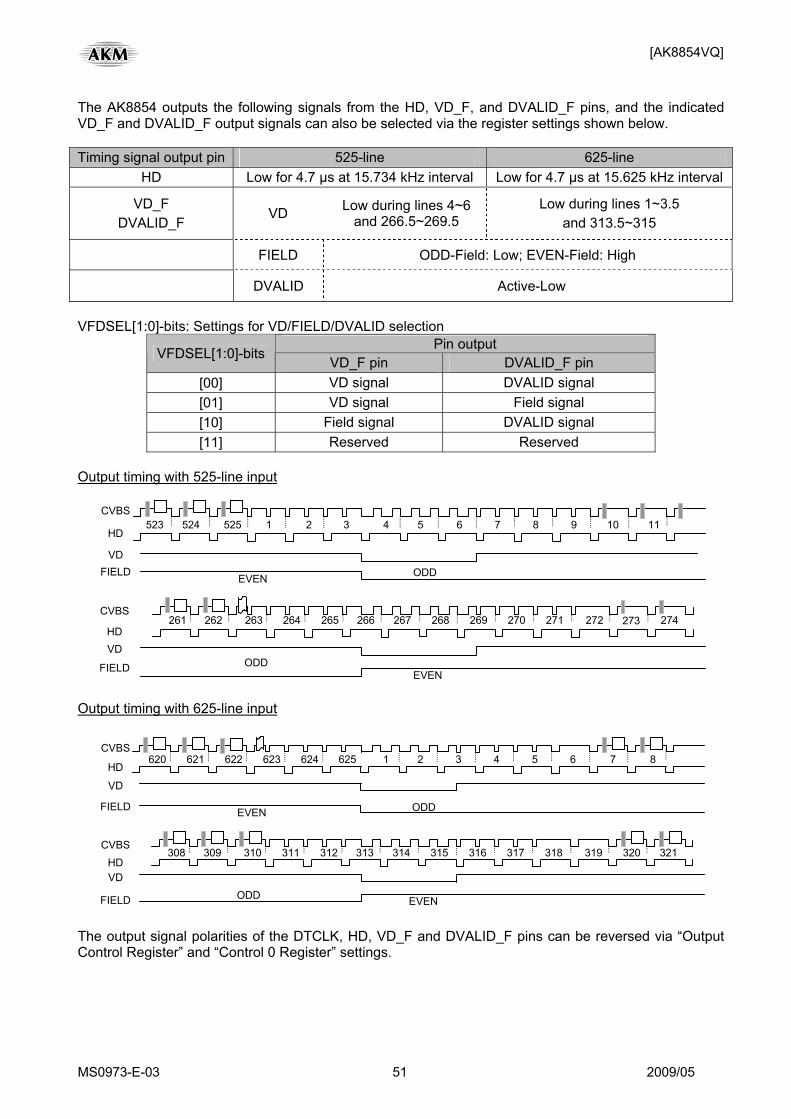
The AK8854 outputs the following signals from the HD, VD_F, and DVALID_F pins, and the indicated VD_F and DVALID_F output signals can also be selected via the register settings shown below. Timing signal output pin 525-line 625-line
HD Low for 4.7 µs at 15.734 kHz interval Low for 4.7 µs at 15.625 kHz interval
VD_F DVALID_F
VD Low during lines 4~6 and 266.5~269.5
Low during lines 1~3.5 and 313.5~315
FIELD ODD-Field: Low; EVEN-Field: High
DVALID Active-Low
VFDSEL[1:0]-bits: Settings for VD/FIELD/DVALID selection
Pin output VFDSEL[1:0]-bits VD_F pin DVALID_F pin
[00] VD signal DVALID signal [01] VD signal Field signal [10] Field signal DVALID signal [11] Reserved Reserved
Output timing with 525-line input
EVEN ODD
523 524 525 1 2 3 4 5 6 7 8 9 10 11
VD FIELD
HD
CVBS
EVENODD
264 265 266 267 268 269 270 271 263 262 272 273 274261
FIELD
VD
CVBS
HD
Output timing with 625-line input
HD
VD
FIELD EVEN ODD
CVBS 620 621 622 623 624 625 1 2 3 4 5 6 87
HD VD
EVENODD FIELD
CVBS 311 312 313 314 315 316 317 318 310 309 319 321308 320
The output signal polarities of the DTCLK, HD, VD_F and DVALID_F pins can be reversed via “Output Control Register” and “Control 0 Register” settings.
[AK8854VQ]
MS0973-E-03 52 2009/05
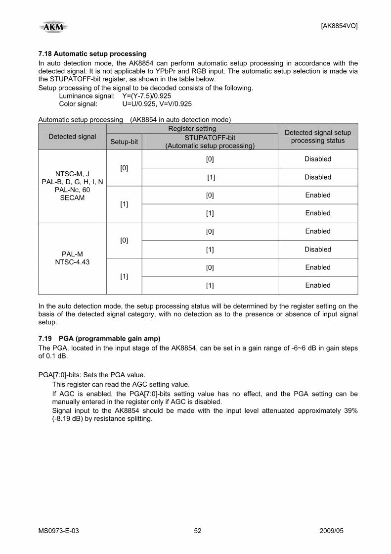
7.18 Automatic setup processing In auto detection mode, the AK8854 can perform automatic setup processing in accordance with the detected signal. It is not applicable to YPbPr and RGB input. The automatic setup selection is made via the STUPATOFF-bit register, as shown in the table below. Setup processing of the signal to be decoded consists of the following.
Luminance signal: Y=(Y-7.5)/0.925 Color signal: U=U/0.925, V=V/0.925
Automatic setup processing (AK8854 in auto detection mode)
Register setting Detected signal
Setup-bit STUPATOFF-bit (Automatic setup processing)
Detected signal setup processing status
[0] Disabled [0]
[1] Disabled
[0] Enabled
NTSC-M, J PAL-B, D, G, H, I, N
PAL-Nc, 60 SECAM
[1] [1] Enabled
[0] Enabled [0]
[1] Disabled
[0] Enabled
PAL-M NTSC-4.43
[1] [1] Enabled
In the auto detection mode, the setup processing status will be determined by the register setting on the basis of the detected signal category, with no detection as to the presence or absence of input signal setup. 7.19 PGA (programmable gain amp) The PGA, located in the input stage of the AK8854, can be set in a gain range of -6~6 dB in gain steps of 0.1 dB. PGA[7:0]-bits: Sets the PGA value. This register can read the AGC setting value. If AGC is enabled, the PGA[7:0]-bits setting value has no effect, and the PGA setting can be
manually entered in the register only if AGC is disabled. Signal input to the AK8854 should be made with the input level attenuated approximately 39%
(-8.19 dB) by resistance splitting.
[AK8854VQ]
MS0973-E-03 53 2009/05
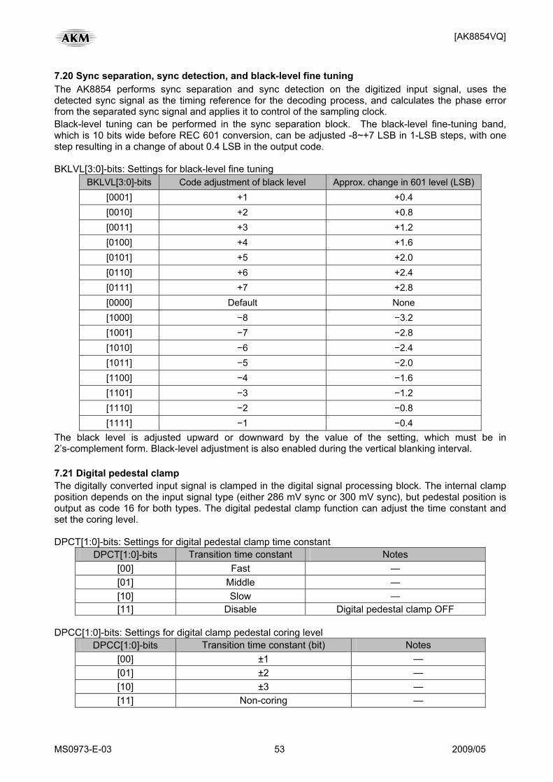
7.20 Sync separation, sync detection, and black-level fine tuning The AK8854 performs sync separation and sync detection on the digitized input signal, uses the detected sync signal as the timing reference for the decoding process, and calculates the phase error from the separated sync signal and applies it to control of the sampling clock. Black-level tuning can be performed in the sync separation block. The black-level fine-tuning band, which is 10 bits wide before REC 601 conversion, can be adjusted -8~+7 LSB in 1-LSB steps, with one step resulting in a change of about 0.4 LSB in the output code. BKLVL[3:0]-bits: Settings for black-level fine tuning
BKLVL[3:0]-bits Code adjustment of black level Approx. change in 601 level (LSB)[0001] +1 +0.4 [0010] +2 +0.8 [0011] +3 +1.2 [0100] +4 +1.6 [0101] +5 +2.0 [0110] +6 +2.4 [0111] +7 +2.8 [0000] Default None [1000] −8 −3.2 [1001] −7 −2.8 [1010] −6 −2.4 [1011] −5 −2.0 [1100] −4 −1.6 [1101] −3 −1.2 [1110] −2 −0.8 [1111] −1 −0.4
The black level is adjusted upward or downward by the value of the setting, which must be in 2’s-complement form. Black-level adjustment is also enabled during the vertical blanking interval. 7.21 Digital pedestal clamp The digitally converted input signal is clamped in the digital signal processing block. The internal clamp position depends on the input signal type (either 286 mV sync or 300 mV sync), but pedestal position is output as code 16 for both types. The digital pedestal clamp function can adjust the time constant and set the coring level. DPCT[1:0]-bits: Settings for digital pedestal clamp time constant
DPCT[1:0]-bits Transition time constant Notes [00] Fast — [01] Middle — [10] Slow — [11] Disable Digital pedestal clamp OFF
DPCC[1:0]-bits: Settings for digital clamp pedestal coring level
DPCC[1:0]-bits Transition time constant (bit) Notes [00] ±1 — [01] ±2 — [10] ±3 — [11] Non-coring —
[AK8854VQ]
MS0973-E-03 54 2009/05
7.22 Color killer In CVBS or S-video input, the chroma signal quality of the input signal is determined by comparison of its color burst level against the threshold setting in the color killer control register. If the level is below the threshold, the color killer is activated, resulting in processing of the input as a monochrome signal and thus with CbCr data fixed at 0x80. Depending on the register setting, the color killer may also be activated by failure of the color decode PLL lock. COLKILL-bit: Settings for color killer ON and OFF
COLKILL-bit Notes [0] Enable — [1] Disable —
CKLVL[3:0]-bits: For threshold setting; default setting [1000] = −23dB. CKSCM[1:0]-bits: Used for threshold setting with SECAM input; expands 2-bit for CKLVL[3:0]-bit CKILSEL: Settings for color killer activation
CKILSEL-bit Condition for activation Notes[0] Burst level below threshold setting in CKLVL[3:0]-bits —
[1] Burst level below threshold setting in CKLVL[3:0]-bits, or Failure of color decode PLL lock —
7.23 Image quality adjustments Image quality adjustments consist of contrast, brightness, sharpness, color saturation, and hue adjustment. All image quality adjustments are disabled during the vertical blanking interval, but contrast and brightness adjustment can be enabled by the register setting. 7.23.1 Contrast adjustment CONT[7:0]-bits: For contrast adjustment; default value 0x80 (no adjustment) Contrast adjustment involves multiplication by the gain factor setting in this register. The equation
of the multiplication can be modified by register setting as follows. If CONTSEL = [0], then YOUT = (CONT/128) x (YIN – 128) + 128 If CONTSEL = [1], then YOUT = (CONT/128) x YIN YOUT: Contrast obtained by the calculation YIN: Contrast before the calculation CONT: Contrast gain factor (register setting value) The gain factor can be set in the range 0~255. If the calculated value is outside the specified
contrast range, it is clipped to the upper ‘254’ or lower ‘1’ limit. With a control bit 601LIMIT setting of [1], the output will be in the range 16~235.
CONTSEL-bit: Settings for contrast adjustment Inclination
CONTSEL -bit Inclination Notes [0] Toward luminance of 128 — [1] Toward luminance of 0 —
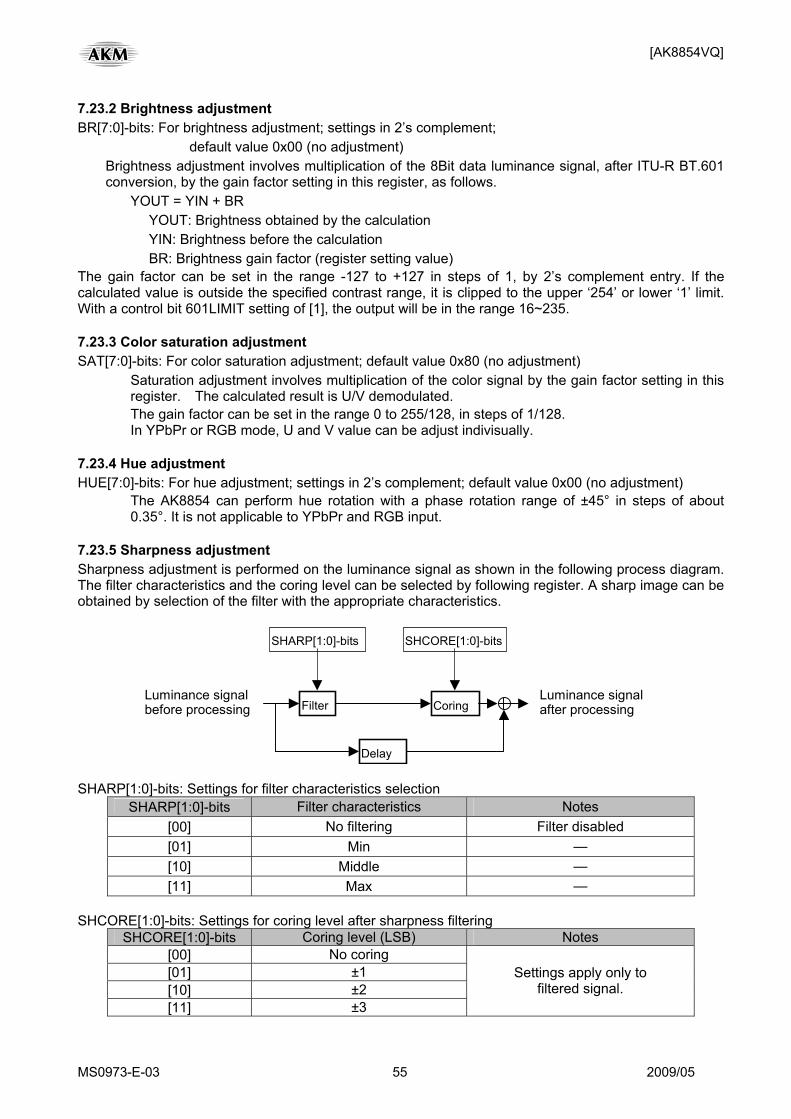
[AK8854VQ]
MS0973-E-03 55 2009/05
7.23.2 Brightness adjustment BR[7:0]-bits: For brightness adjustment; settings in 2’s complement; default value 0x00 (no adjustment) Brightness adjustment involves multiplication of the 8Bit data luminance signal, after ITU-R BT.601
conversion, by the gain factor setting in this register, as follows. YOUT = YIN + BR YOUT: Brightness obtained by the calculation YIN: Brightness before the calculation BR: Brightness gain factor (register setting value) The gain factor can be set in the range -127 to +127 in steps of 1, by 2’s complement entry. If the calculated value is outside the specified contrast range, it is clipped to the upper ‘254’ or lower ‘1’ limit. With a control bit 601LIMIT setting of [1], the output will be in the range 16~235. 7.23.3 Color saturation adjustment SAT[7:0]-bits: For color saturation adjustment; default value 0x80 (no adjustment) Saturation adjustment involves multiplication of the color signal by the gain factor setting in this
register. The calculated result is U/V demodulated. The gain factor can be set in the range 0 to 255/128, in steps of 1/128. In YPbPr or RGB mode, U and V value can be adjust indivisually. 7.23.4 Hue adjustment HUE[7:0]-bits: For hue adjustment; settings in 2’s complement; default value 0x00 (no adjustment) The AK8854 can perform hue rotation with a phase rotation range of ±45° in steps of about
0.35°. It is not applicable to YPbPr and RGB input. 7.23.5 Sharpness adjustment Sharpness adjustment is performed on the luminance signal as shown in the following process diagram. The filter characteristics and the coring level can be selected by following register. A sharp image can be obtained by selection of the filter with the appropriate characteristics.
Filter Coring
Delay
Luminance signal before processing
SHARP[1:0]-bits SHCORE[1:0]-bits
Luminance signal after processing
SHARP[1:0]-bits: Settings for filter characteristics selection
SHARP[1:0]-bits Filter characteristics Notes [00] No filtering Filter disabled [01] Min — [10] Middle — [11] Max —
SHCORE[1:0]-bits: Settings for coring level after sharpness filtering
SHCORE[1:0]-bits Coring level (LSB) Notes [00] No coring [01] ±1 [10] ±2 [11] ±3
Settings apply only to filtered signal.
[AK8854VQ]
MS0973-E-03 56 2009/05
VBIIMGCTL-bit: Settings for brightness and contrast adjustment status (ON/OFF) during VBI
VBIIMGCTL -bit Status during VBI Notes [0] Disabled — [1] Enabled —
VBIIMGCTL-bit must be set [1] when input signal is YPbPr or RGB. 7.24 Luminance bandwidth adjustment Luminance bandwidth adjustment can be performed for MPEG compression etc. The band-limiting filters for pre-compression limiting can be selected by the following register settings. Without these filters, the frequency response of the luminance signal is determined by the decimation filter. LUMFIL[1:0]-bits: Settings for luminance bandwidth filter
LUMFIL[1:0]-bits Filter characteristic Notes [00] No filter -3 dB at 6.29 MHz [01] Narrow -3dB at 2.94MHz [10] Mid -3dB at 3.30MHz [11] Wide -3dB at 4.00MHz
7.25 Sepia output Sepia-colored output of the decoded signal can be obtained by the following register setting. SEPIA-bit: Settings for sepia output of decoded signal
SEPIA –bit Output Notes [0] Normal — [1] Sepia —
7.26 VBI information decoding The AK8854 decodes closed-caption, closed-caption-extended, VBID(CGMS), and WSS signals on the vertical blanking signal, and writes the decoded data into a storage register. The AK8854 reads each data bit in Request VBI Information Register(R/W)-[3:0] as a decoding request and thereupon enters a data wait state. Data detection and decoding to the storage register are then performed which indicates the presence or absence of data at STATUS 2 Register-[3:0] for host. The host can therefore determine the stored values by reading the respective storage registers. The value in each storage register is retained until a new value is written in by data renewal. For VBID data (CGMS-A), the CRCC code is decoded and only the arithmetic result is stored in the register.
Signal type Superimposed line line Closed Caption Line21 (NTSC-M, J, NTSC-4.43, PAL-M, 60) 525
Closed Caption Extended Data Line284 (NTSC-M, J, NTSC-4.43, PAL-M, 60) 525
VBID Line20 / 283 (NTSC-M, J, NTSC-4.43, PAL-M, 60) Line20 / 333 (PAL-B, D, G, H, I, N, Nc, SECAM)
525 625
WSS Line23 (PAL-B, D, G, H, I, N, Nc, SECAM) 625 The storage registers for each of the signal types are as follows. For storage bit allocations, please refer to the respective register setting descriptions. Closed Caption 1 Register, Closed Caption 2 Register WSS 1 Register, WSS 2 Register Extended Data 1 Register, Extended Data 2 Register VBID 1 Register, VBID 2 Register
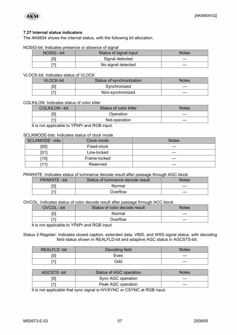
[AK8854VQ]
MS0973-E-03 57 2009/05
7.27 Internal status indicators The AK8854 shows the internal status, with the following bit allocation. NOSIG-bit: Indicates presence or absence of signal
NOSIG –bit Status of signal input Notes [0] Signal detected — [1] No signal detected —
VLOCK-bit: Indicates status of VLOCK
VLOCK-bit Status of synchronization Notes [0] Synchronized — [1] Non-synchronized —
COLKILON: Indicates status of color killer
COLKILON –bit Status of color killer Notes [0] Operation — [1] Not-operation —
It is not applicable to YPbPr and RGB input. SCLKMODE-bits: Indicates status of clock mode
SCLKMODE –bits Clock mode Notes [00] Fixed-clock — [01] Line-locked — [10] Frame-locked — [11] Reserved —
PKWHITE: Indicates status of luminance decode result after passage through AGC block
PKWHITE –bit Status of luminance decode result Notes [0] Normal — [1] Overflow —
OVCOL: Indicates status of color decode result after passage through ACC block
OVCOL –bit Status of color decode result Notes [0] Normal — [1] Overflow —
It is not applicable to YPbPr and RGB input. Status 2-Ragister: Indicates closed caption, extended data, VBID, and WSS signal status, with decoding
field status shown in REALFLD-bit and adaptive AGC status in AGCSTS-bit.
REALFLD -bit Decoding field Notes [0] Even — [1] Odd —
AGCSTS -bit Status of AGC operation Notes
[0] Sync AGC operation — [1] Peak AGC operation —
It is not applicable that sync signal is H/VSYNC or CSYNC at RGB input.
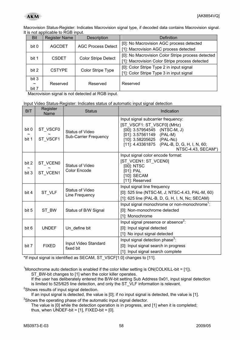
[AK8854VQ]
MS0973-E-03 58 2009/05
Macrovision Status-Register: Indicates Macrovision signal type, if decoded data contains Macrovision signal. It is not applicable to RGB input.
Bit Register Name Description Definition
bit 0 AGCDET AGC Process Detect[0]: No Macrovision AGC process detected [1]: Macrovision AGC process detected
bit 1 CSDET Color Stripe Detect [0]: No Macrovision Color Stripe process detected[1]: Macrovision Color Stripe process detected
bit 2 CSTYPE Color Stripe Type [0]: Color Stripe Type 2 in input signal [1]: Color Stripe Type 3 in input signal
bit 3 ~
bit 7 Reserved Reserved Reserved
Macrovision signal is not detected at RGB input. Input Video Status-Register: Indicates status of automatic input signal detection
BIT Register Name Status Indication
bit 0 ~
bit 1
ST_VSCF0 ~
ST_VSCF1
Status of Video Sub-Carrier Frequency
Input signal subcarrier frequency: [ST_VSCF1: ST_VSCF0] (MHz) [00]: 3.57954545 (NTSC-M, J) [01]: 3.57561149 (PAL-M) [10]: 3.58205625 (PAL-Nc) [11]: 4.43361875 (PAL-B, D, G, H, I, N, 60; NTSC-4.43, SECAM*)
bit 2 ~
bit 3
ST_VCEN0 ~
ST_VCEN1
Status of Video Color Encode
Input signal color encode format: [ST_VCEN1: ST_VCEN0] [00]: NTSC [01]: PAL [10]: SECAM [11]: Reserved
bit 4 ST_VLF Status of Video Line Frequency
Input signal line frequency [0]: 525 line (NTSC-M, J; NTSC-4.43, PAL-M, 60) [1]: 625 line (PAL-B, D, G, H, I, N, Nc; SECAM)
bit 5 ST_BW Status of B/W Signal Input signal monochrome or non-monochrome1: [0]: Non-monochrome detected [1]: Monochrome
bit 6 UNDEF Un_define bit Input signal presence or absence2: [0]: Input signal detected [1]: No input signal detected
bit 7 FIXED Input Video Standard fixed bit
Input signal detection phase3: [0]: Input signal search in progress [1]: Input signal search complete
*If input signal is identified as SECAM, ST_VSCF[1:0] changes to [11]. 1Monochrome auto detection is enabled if the color killer setting is ON(COLKILL-bit = [1]). ST_BW-bit changes to [1] when the color killer operates. If the user has deliberately entered the B/W-bit setting Sub Address 0x01, input signal detection is limited to 525/625 line detection, and only the ST_VLF information is relevant. 2Shows results of input signal detection. If an input signal is detected, the value is [0]; if no input signal is detected, the value is [1]. 3Shows the operating phase of the automatic input signal detector. The value is [0] while the detection operation is in progress, and [1] when it is completed; thus, when UNDEF-bit = [1], FIXED-bit = [0].
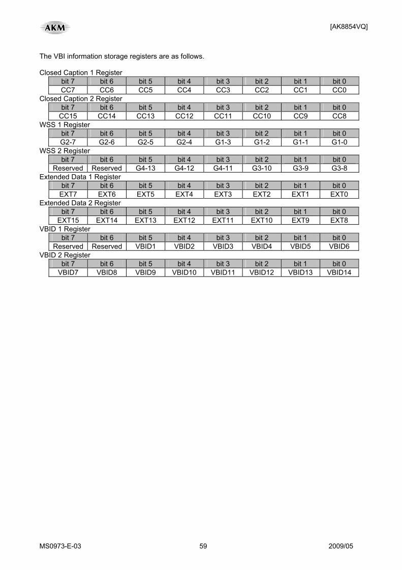
[AK8854VQ]
MS0973-E-03 59 2009/05
The VBI information storage registers are as follows. Closed Caption 1 Register
bit 7 bit 6 bit 5 bit 4 bit 3 bit 2 bit 1 bit 0 CC7 CC6 CC5 CC4 CC3 CC2 CC1 CC0
Closed Caption 2 Register bit 7 bit 6 bit 5 bit 4 bit 3 bit 2 bit 1 bit 0
CC15 CC14 CC13 CC12 CC11 CC10 CC9 CC8 WSS 1 Register
bit 7 bit 6 bit 5 bit 4 bit 3 bit 2 bit 1 bit 0 G2-7 G2-6 G2-5 G2-4 G1-3 G1-2 G1-1 G1-0
WSS 2 Register bit 7 bit 6 bit 5 bit 4 bit 3 bit 2 bit 1 bit 0
Reserved Reserved G4-13 G4-12 G4-11 G3-10 G3-9 G3-8 Extended Data 1 Register
bit 7 bit 6 bit 5 bit 4 bit 3 bit 2 bit 1 bit 0 EXT7 EXT6 EXT5 EXT4 EXT3 EXT2 EXT1 EXT0
Extended Data 2 Register bit 7 bit 6 bit 5 bit 4 bit 3 bit 2 bit 1 bit 0
EXT15 EXT14 EXT13 EXT12 EXT11 EXT10 EXT9 EXT8 VBID 1 Register
bit 7 bit 6 bit 5 bit 4 bit 3 bit 2 bit 1 bit 0 Reserved Reserved VBID1 VBID2 VBID3 VBID4 VBID5 VBID6
VBID 2 Register bit 7 bit 6 bit 5 bit 4 bit 3 bit 2 bit 1 bit 0
VBID7 VBID8 VBID9 VBID10 VBID11 VBID12 VBID13 VBID14
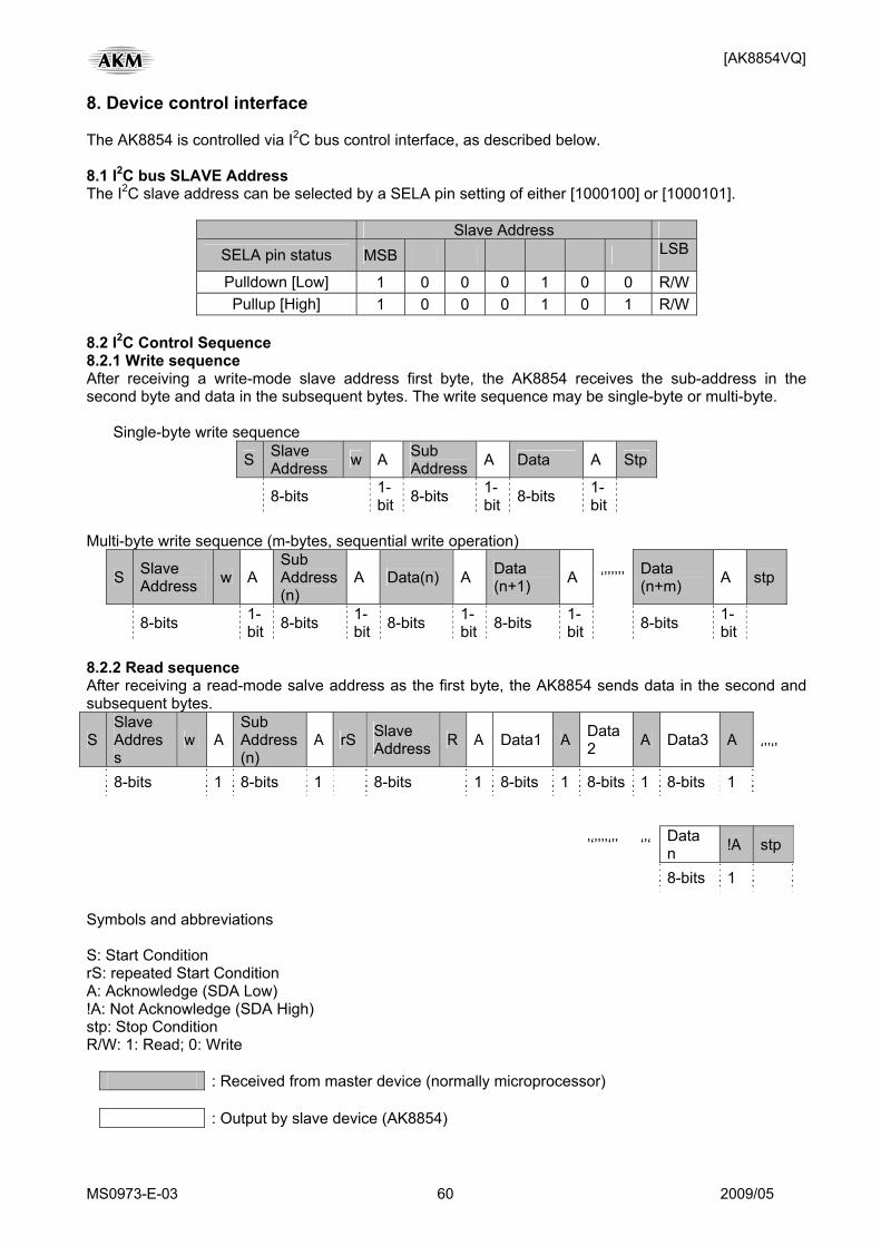
[AK8854VQ]
MS0973-E-03 60 2009/05
8. Device control interface The AK8854 is controlled via I2C bus control interface, as described below. 8.1 I2C bus SLAVE Address The I2C slave address can be selected by a SELA pin setting of either [1000100] or [1000101].
Slave Address SELA pin status MSB LSB
Pulldown [Low] 1 0 0 0 1 0 0 R/W Pullup [High] 1 0 0 0 1 0 1 R/W
8.2 I2C Control Sequence 8.2.1 Write sequence After receiving a write-mode slave address first byte, the AK8854 receives the sub-address in the second byte and data in the subsequent bytes. The write sequence may be single-byte or multi-byte. Single-byte write sequence
S Slave Address w A Sub
Address A Data A Stp
8-bits 1-bit 8-bits 1-
bit 8-bits 1-bit
Multi-byte write sequence (m-bytes, sequential write operation)
S Slave Address w A
Sub Address(n)
A Data(n) A Data (n+1) A Data
(n+m) A stp
8-bits 1-bit 8-bits 1-
bit 8-bits 1-bit 8-bits 1-
bit
‘’’’’’’
8-bits 1-bit
8.2.2 Read sequence After receiving a read-mode salve address as the first byte, the AK8854 sends data in the second and subsequent bytes.
S Slave Address
w A Sub Address(n)
A rS Slave Address R A Data1 A Data
2 A Data3 A ‘’’‘’
8-bits 1 8-bits 1 8-bits 1 8-bits 1 8-bits 1 8-bits 1
’‘’’’’‘’’ ‘’‘ Data n !A stp
8-bits 1 Symbols and abbreviations S: Start Condition rS: repeated Start Condition A: Acknowledge (SDA Low) !A: Not Acknowledge (SDA High) stp: Stop Condition R/W: 1: Read; 0: Write
: Received from master device (normally microprocessor) : Output by slave device (AK8854)
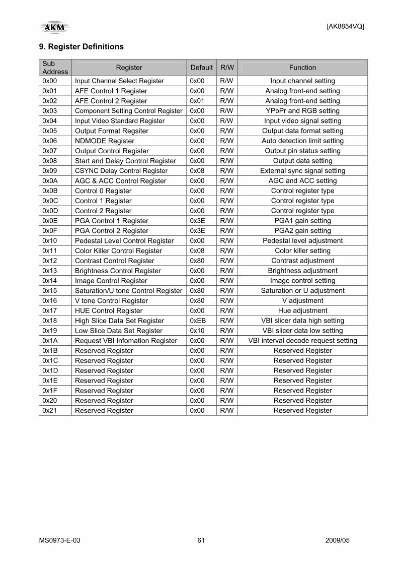
[AK8854VQ]
MS0973-E-03 61 2009/05
9. Register Definitions Sub Address Register Default R/W Function
0x00 Input Channel Select Register 0x00 R/W Input channel setting 0x01 AFE Control 1 Register 0x00 R/W Analog front-end setting 0x02 AFE Control 2 Register 0x01 R/W Analog front-end setting 0x03 Component Setting Control Register 0x00 R/W YPbPr and RGB setting 0x04 Input Video Standard Register 0x00 R/W Input video signal setting 0x05 Output Format Regsiter 0x00 R/W Output data format setting 0x06 NDMODE Register 0x00 R/W Auto detection limit setting 0x07 Output Control Register 0x00 R/W Output pin status setting 0x08 Start and Delay Control Register 0x00 R/W Output data setting 0x09 CSYNC Delay Control Register 0x08 R/W External sync signal setting 0x0A AGC & ACC Control Register 0x00 R/W AGC and ACC setting 0x0B Control 0 Register 0x00 R/W Control register type 0x0C Control 1 Register 0x00 R/W Control register type 0x0D Control 2 Register 0x00 R/W Control register type 0x0E PGA Control 1 Register 0x3E R/W PGA1 gain setting 0x0F PGA Control 2 Register 0x3E R/W PGA2 gain setting 0x10 Pedestal Level Control Register 0x00 R/W Pedestal level adjustment 0x11 Color Killer Control Register 0x08 R/W Color killer setting 0x12 Contrast Control Register 0x80 R/W Contrast adjustment 0x13 Brightness Control Register 0x00 R/W Brightness adjustment 0x14 Image Control Register 0x00 R/W Image control setting 0x15 Saturation/U tone Control Register 0x80 R/W Saturation or U adjustment 0x16 V tone Control Register 0x80 R/W V adjustment 0x17 HUE Control Register 0x00 R/W Hue adjustment 0x18 High Slice Data Set Register 0xEB R/W VBI slicer data high setting 0x19 Low Slice Data Set Register 0x10 R/W VBI slicer data low setting 0x1A Request VBI Infomation Register 0x00 R/W VBI interval decode request setting 0x1B Reserved Register 0x00 R/W Reserved Register 0x1C Reserved Register 0x00 R/W Reserved Register 0x1D Reserved Register 0x00 R/W Reserved Register 0x1E Reserved Register 0x00 R/W Reserved Register 0x1F Reserved Register 0x00 R/W Reserved Register 0x20 Reserved Register 0x00 R/W Reserved Register 0x21 Reserved Register 0x00 R/W Reserved Register
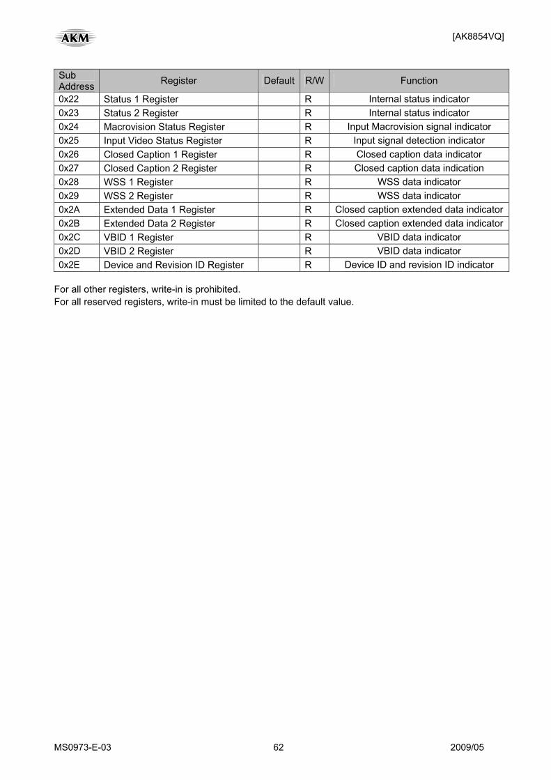
[AK8854VQ]
MS0973-E-03 62 2009/05
Sub Address Register Default R/W Function
0x22 Status 1 Register R Internal status indicator 0x23 Status 2 Register R Internal status indicator 0x24 Macrovision Status Register R Input Macrovision signal indicator 0x25 Input Video Status Register R Input signal detection indicator 0x26 Closed Caption 1 Register R Closed caption data indicator 0x27 Closed Caption 2 Register R Closed caption data indication 0x28 WSS 1 Register R WSS data indicator 0x29 WSS 2 Register R WSS data indicator 0x2A Extended Data 1 Register R Closed caption extended data indicator0x2B Extended Data 2 Register R Closed caption extended data indicator0x2C VBID 1 Register R VBID data indicator 0x2D VBID 2 Register R VBID data indicator 0x2E Device and Revision ID Register R Device ID and revision ID indicator
For all other registers, write-in is prohibited. For all reserved registers, write-in must be limited to the default value.
[AK8854VQ]
MS0973-E-03 63 2009/05
10. Register settings overview Input Channel Select Register (R/W) [Sub Address 0x00], for input signal selection Sub Address 0x00 Default Value: 0x00
bit 7 bit 6 bit 5 bit 4 bit 3 bit 2 bit 1 bit 0 AINSEL7 AINSEL6 AINSEL5 AINSEL4 AINSEL3 AINSEL2 AINSEL1 AINSEL0 Default Value 0 0 0 0 0 0 0 0 Input Channel Select Register Definition
Bit Register Name R / W Definition
bit 0 ~ bit 7
AINSEL0 ~ AINSEL7
Analog Input Select R / W
Input video signal selection: [00000000]: AIN1 (CVBS) [00000001]: AIN2 (CVBS) [00000010]: AIN3(CVBS) [00000011]: AIN4 (CVBS) [00000100]: AIN5 (CVBS) [00000101]: AIN6 (CVBS) [00001101]: AIN6(Y) / AIN7(C) [00011100]: AIN5(Y) / AIN8(C) [00100011]: AIN4(Y) / AIN9(C) [01100010]: AIN3(Y) / AIN10(C) [00101101]: AIN6(Y) / AIN7(Pb) / AIN9(Pr) [10101101]: AIN6(G) / AIN7(R) / AIN9(B) [01111100]: AIN5(Y) / AIN8(Pb) / AIN10(Pr) [11111100]: AIN5 (G)/ AIN8(R) / AIN10(B)
[AK8854VQ]
MS0973-E-03 64 2009/05
AFE Control Register 1 (R/W) [Sub Address 0x01], for analog front end Sub Address 0x01 Default Value : 0x00
bit 7 bit 6 bit 5 bit 4 bit 3 bit 2 bit 1 bit 0 CLPWIDTH1 CLPWIDTH0 CLPSTAT1 CLPSTAT0 Reserved BCLPSTAT2 BCLPSTAT1 BCLPSTAT0Default Value 0 0 0 0 0 0 0 0 AFE Control Register 1 Definition
Bit Register Name R / W Definition
bit 0 ~ bit 2
BCLPSTAT0 ~ BCLPSTAT2
Back Porch Clamp Start R / W
Set the position of analog backporch clamp pulse.[ BCLPSTAT2 : BCLPSTAT0 ] [000]: Same position with “CLPSTAT” setting [001]: (1/128)H delay from “CLPSTAT” setting [010]: (2/128)H delay from “CLPSTAT” setting [011]: (3/128)H delay from “CLPSTAT” setting [100]: (4/128)H advance from “CLPSTAT” setting [101]: (3/128)H advance from “CLPSTAT” setting [110]: (2/128)H advance from “CLPSTAT” setting [111]: (1/128)H advance from “CLPSTAT” setting
bit 3 Reserved Reserved R Reserved
bit 4 ~ bit 5
CLPSTAT0 ~ CLPSTAT1
Clamp Start R / W
Set the position of clamp pulse [ CLPSTAT1 : CLPSTAT0 ] [00] : Sync tip/ middle/ bottom clamp:
Centor of horizontal sync Back porch clamp:
Centor of backporch interval [01] : (1/128) H delay [10] : (2/128) H advance [11] : (1/128) H advance
bit 6 ~ bit 7
CLPWIDTH0 ~ CLPWIDTH1
Clamp Pulse Width R / W
Set the width of clamp pulse. [ CLPWIDTH1 : CLPWIDTH0 ] [00] : 275nsec [01] : 555nsec [10] : 1.1usec [11] : 2.2usec
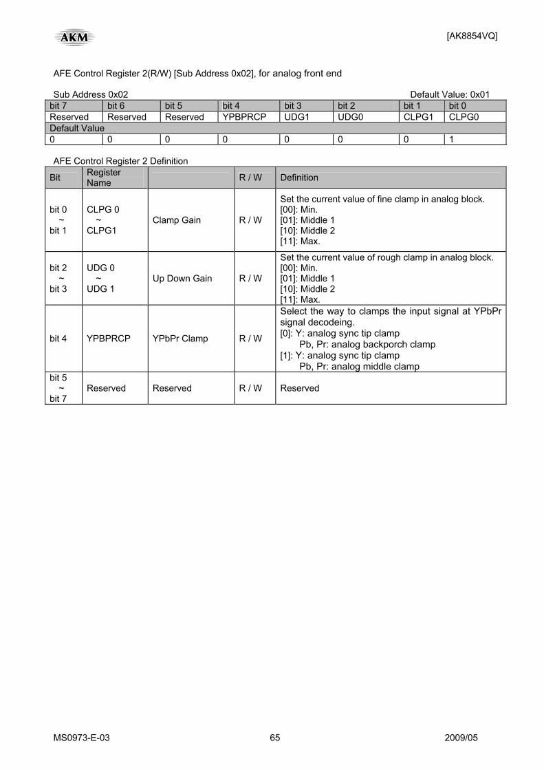
[AK8854VQ]
MS0973-E-03 65 2009/05
AFE Control Register 2(R/W) [Sub Address 0x02], for analog front end Sub Address 0x02 Default Value: 0x01
bit 7 bit 6 bit 5 bit 4 bit 3 bit 2 bit 1 bit 0 Reserved Reserved Reserved YPBPRCP UDG1 UDG0 CLPG1 CLPG0 Default Value 0 0 0 0 0 0 0 1 AFE Control Register 2 Definition
Bit Register Name R / W Definition
bit 0 ~
bit 1
CLPG 0 ~
CLPG1 Clamp Gain R / W
Set the current value of fine clamp in analog block. [00]: Min. [01]: Middle 1 [10]: Middle 2 [11]: Max.
bit 2 ~
bit 3
UDG 0 ~
UDG 1 Up Down Gain R / W
Set the current value of rough clamp in analog block. [00]: Min. [01]: Middle 1 [10]: Middle 2 [11]: Max.
bit 4 YPBPRCP YPbPr Clamp R / W
Select the way to clamps the input signal at YPbPr signal decodeing. [0]: Y: analog sync tip clamp
Pb, Pr: analog backporch clamp [1]: Y: analog sync tip clamp
Pb, Pr: analog middle clamp bit 5
~ bit 7
Reserved Reserved R / W Reserved
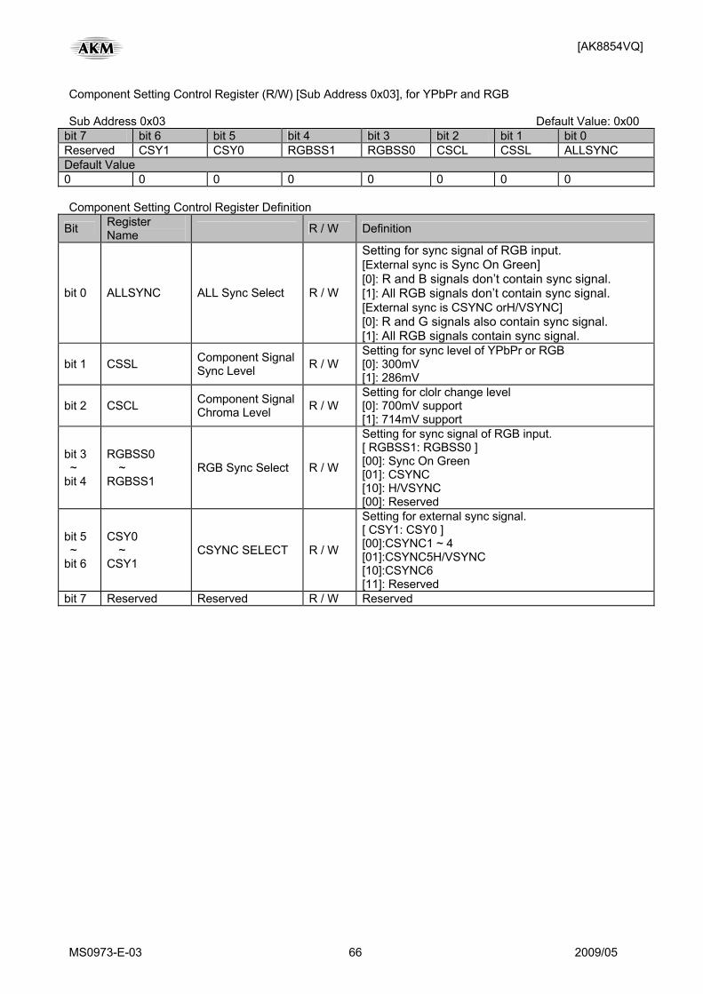
[AK8854VQ]
MS0973-E-03 66 2009/05
Component Setting Control Register (R/W) [Sub Address 0x03], for YPbPr and RGB Sub Address 0x03 Default Value: 0x00
bit 7 bit 6 bit 5 bit 4 bit 3 bit 2 bit 1 bit 0 Reserved CSY1 CSY0 RGBSS1 RGBSS0 CSCL CSSL ALLSYNC Default Value 0 0 0 0 0 0 0 0 Component Setting Control Register Definition
Bit Register Name R / W Definition
bit 0 ALLSYNC ALL Sync Select R / W
Setting for sync signal of RGB input. [External sync is Sync On Green] [0]: R and B signals don’t contain sync signal. [1]: All RGB signals don’t contain sync signal. [External sync is CSYNC orH/VSYNC] [0]: R and G signals also contain sync signal. [1]: All RGB signals contain sync signal.
bit 1 CSSL Component SignalSync Level R / W
Setting for sync level of YPbPr or RGB [0]: 300mV [1]: 286mV
bit 2 CSCL Component SignalChroma Level R / W
Setting for clolr change level [0]: 700mV support [1]: 714mV support
bit 3 ~ bit 4
RGBSS0 ~
RGBSS1 RGB Sync Select R / W
Setting for sync signal of RGB input. [ RGBSS1: RGBSS0 ] [00]: Sync On Green [01]: CSYNC [10]: H/VSYNC [00]: Reserved
bit 5 ~ bit 6
CSY0 ~
CSY1 CSYNC SELECT R / W
Setting for external sync signal. [ CSY1: CSY0 ] [00]:CSYNC1 ~ 4 [01]:CSYNC5H/VSYNC [10]:CSYNC6 [11]: Reserved
bit 7 Reserved Reserved R / W Reserved
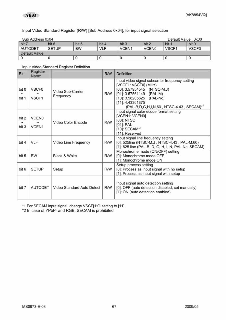
[AK8854VQ]
MS0973-E-03 67 2009/05
Input Video Standard Register (R/W) [Sub Address 0x04], for input signal selection Sub Address 0x04 Default Value : 0x00
bit 7 bit 6 bit 5 bit 4 bit 3 bit 2 bit 1 bit 0 AUTODET SETUP BW VLF VCEN1 VCEN0 VSCF1 VSCF0 Default Value 0 0 0 0 0 0 0 0 Input Video Standard Register Definition
Bit Register Name R/W Definition
bit 0 ~ bit 1
VSCF0 ~ VSCF1
Video Sub-Carrier Frequency R/W
Input video signal subcarrier frequency setting [VSCF1: VSCF0] (MHz) [00]: 3.57954545 (NTSC-M,J) [01]: 3.57561149 (PAL-M) [10]: 3.58205625 (PAL-Nc) [11]: 4.43361875 (PAL-B,D,G,H,I,N,60 , NTSC-4.43 , SECAM)*1
bit 2 ~ bit 3
VCEN0 ~ VCEN1
Video Color Encode R/W
Input signal color ecode format setting [VCEN1: VCEN0] [00]: NTSC [01]: PAL [10]: SECAM*2 [11]: Reserved
bit 4 VLF Video Line Frequency R/WInput signal line frequency setting [0]: 525line (NTSC-M,J , NTSC-4.43 , PAL-M,60) [1]: 625 line (PAL-B, D, G, H, I, N, PAL-Nc, SECAM)
bit 5 BW Black & White R/WMonochrome mode (ON/OFF) setting [0]: Monochrome mode OFF [1]: Monochrome mode ON
bit 6 SETUP Setup R/WSetup process setting [0]: Process as input signal with no setup [1]: Process as input signal with setup
bit 7 AUTODET Video Standard Auto Detect R/WInput signal auto detection setting [0]: OFF (auto detection disabled; set manually) [1]: ON (auto detection enabled)
*1 For SECAM input signal, change VSCF[1:0] setting to [11]. *2 In case of YPbPr and RGB, SECAM is prohibited.
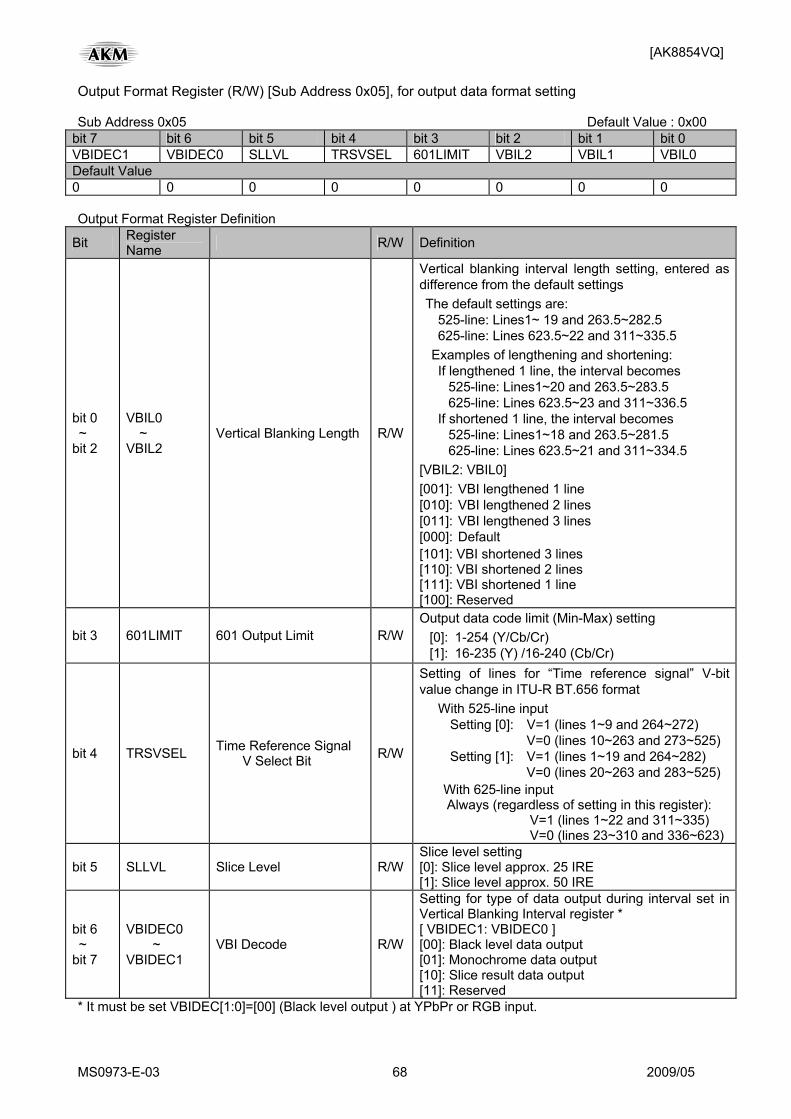
[AK8854VQ]
MS0973-E-03 68 2009/05
Output Format Register (R/W) [Sub Address 0x05], for output data format setting Sub Address 0x05 Default Value : 0x00
bit 7 bit 6 bit 5 bit 4 bit 3 bit 2 bit 1 bit 0 VBIDEC1 VBIDEC0 SLLVL TRSVSEL 601LIMIT VBIL2 VBIL1 VBIL0 Default Value 0 0 0 0 0 0 0 0 Output Format Register Definition
Bit Register Name R/W Definition
bit 0 ~ bit 2
VBIL0 ~ VBIL2
Vertical Blanking Length R/W
Vertical blanking interval length setting, entered as difference from the default settings The default settings are: 525-line: Lines1~ 19 and 263.5~282.5 625-line: Lines 623.5~22 and 311~335.5 Examples of lengthening and shortening: If lengthened 1 line, the interval becomes 525-line: Lines1~20 and 263.5~283.5 625-line: Lines 623.5~23 and 311~336.5 If shortened 1 line, the interval becomes 525-line: Lines1~18 and 263.5~281.5 625-line: Lines 623.5~21 and 311~334.5 [VBIL2: VBIL0] [001]: VBI lengthened 1 line [010]: VBI lengthened 2 lines [011]: VBI lengthened 3 lines [000]: Default [101]: VBI shortened 3 lines [110]: VBI shortened 2 lines [111]: VBI shortened 1 line [100]: Reserved
bit 3 601LIMIT 601 Output Limit R/WOutput data code limit (Min-Max) setting [0]: 1-254 (Y/Cb/Cr) [1]: 16-235 (Y) /16-240 (Cb/Cr)
bit 4 TRSVSEL Time Reference Signal V Select Bit R/W
Setting of lines for “Time reference signal” V-bit value change in ITU-R BT.656 format With 525-line input
Setting [0]: V=1 (lines 1~9 and 264~272) V=0 (lines 10~263 and 273~525) Setting [1]: V=1 (lines 1~19 and 264~282) V=0 (lines 20~263 and 283~525) With 625-line input
Always (regardless of setting in this register): V=1 (lines 1~22 and 311~335) V=0 (lines 23~310 and 336~623)
bit 5 SLLVL Slice Level R/WSlice level setting [0]: Slice level approx. 25 IRE [1]: Slice level approx. 50 IRE
bit 6 ~ bit 7
VBIDEC0 ~ VBIDEC1
VBI Decode R/W
Setting for type of data output during interval set in Vertical Blanking Interval register * [ VBIDEC1: VBIDEC0 ] [00]: Black level data output [01]: Monochrome data output [10]: Slice result data output [11]: Reserved
* It must be set VBIDEC[1:0]=[00] (Black level output ) at YPbPr or RGB input.
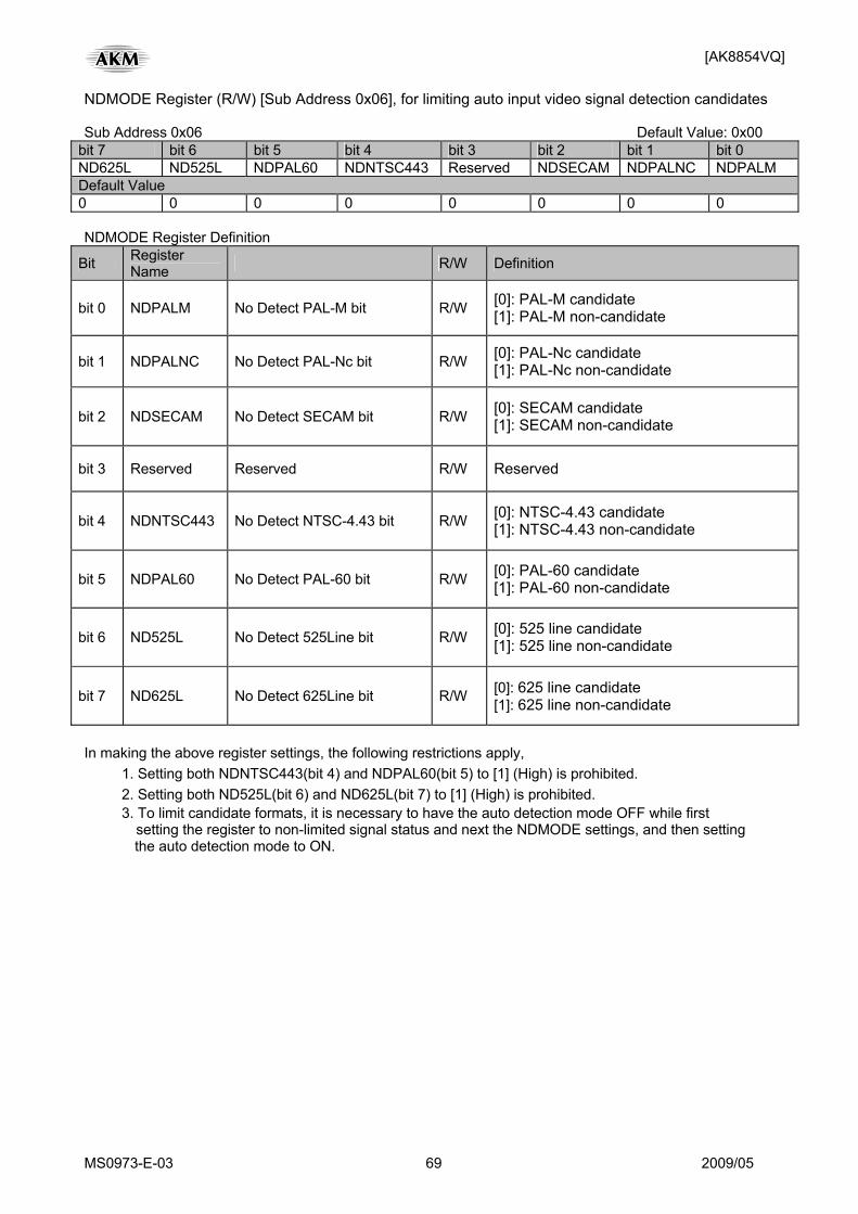
[AK8854VQ]
MS0973-E-03 69 2009/05
NDMODE Register (R/W) [Sub Address 0x06], for limiting auto input video signal detection candidates Sub Address 0x06 Default Value: 0x00
bit 7 bit 6 bit 5 bit 4 bit 3 bit 2 bit 1 bit 0 ND625L ND525L NDPAL60 NDNTSC443 Reserved NDSECAM NDPALNC NDPALM Default Value 0 0 0 0 0 0 0 0 NDMODE Register Definition
Bit Register Name R/W Definition
bit 0 NDPALM No Detect PAL-M bit R/W [0]: PAL-M candidate [1]: PAL-M non-candidate
bit 1 NDPALNC No Detect PAL-Nc bit R/W [0]: PAL-Nc candidate [1]: PAL-Nc non-candidate
bit 2 NDSECAM No Detect SECAM bit R/W [0]: SECAM candidate [1]: SECAM non-candidate
bit 3 Reserved Reserved R/W Reserved
bit 4 NDNTSC443 No Detect NTSC-4.43 bit R/W [0]: NTSC-4.43 candidate [1]: NTSC-4.43 non-candidate
bit 5 NDPAL60 No Detect PAL-60 bit R/W [0]: PAL-60 candidate [1]: PAL-60 non-candidate
bit 6 ND525L No Detect 525Line bit R/W [0]: 525 line candidate [1]: 525 line non-candidate
bit 7 ND625L No Detect 625Line bit R/W [0]: 625 line candidate [1]: 625 line non-candidate
In making the above register settings, the following restrictions apply, 1. Setting both NDNTSC443(bit 4) and NDPAL60(bit 5) to [1] (High) is prohibited. 2. Setting both ND525L(bit 6) and ND625L(bit 7) to [1] (High) is prohibited. 3. To limit candidate formats, it is necessary to have the auto detection mode OFF while first setting the register to non-limited signal status and next the NDMODE settings, and then setting the auto detection mode to ON.
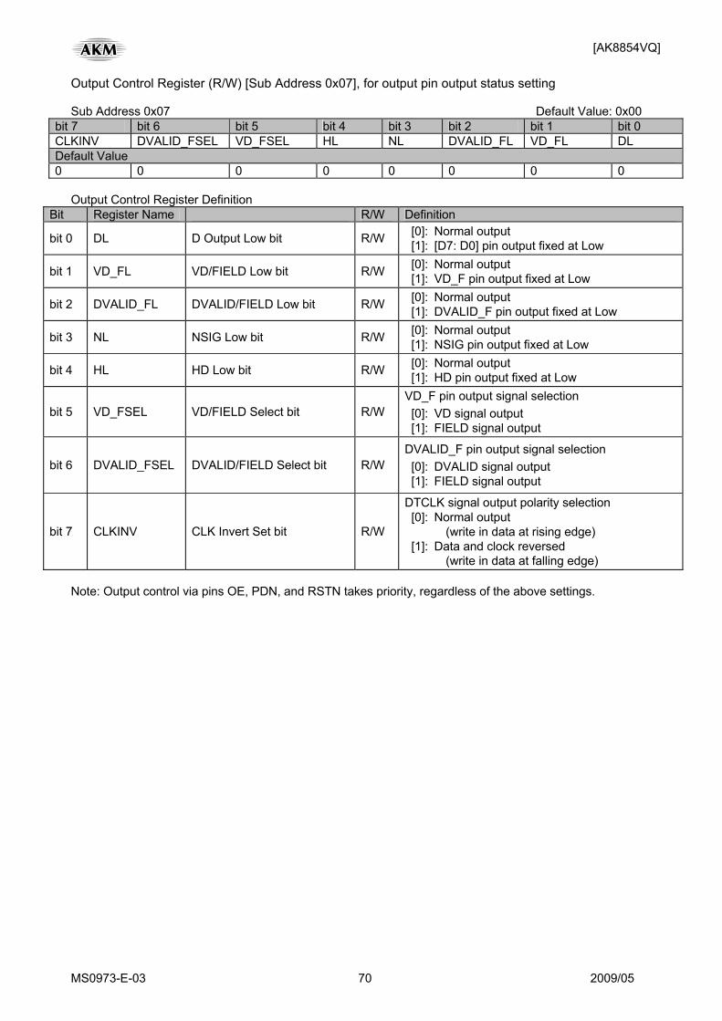
[AK8854VQ]
MS0973-E-03 70 2009/05
Output Control Register (R/W) [Sub Address 0x07], for output pin output status setting Sub Address 0x07 Default Value: 0x00
bit 7 bit 6 bit 5 bit 4 bit 3 bit 2 bit 1 bit 0 CLKINV DVALID_FSEL VD_FSEL HL NL DVALID_FL VD_FL DL Default Value 0 0 0 0 0 0 0 0
Output Control Register Definition
Bit Register Name R/W Definition
bit 0 DL D Output Low bit R/W [0]: Normal output [1]: [D7: D0] pin output fixed at Low
bit 1 VD_FL VD/FIELD Low bit R/W [0]: Normal output [1]: VD_F pin output fixed at Low
bit 2 DVALID_FL DVALID/FIELD Low bit R/W [0]: Normal output [1]: DVALID_F pin output fixed at Low
bit 3 NL NSIG Low bit R/W [0]: Normal output [1]: NSIG pin output fixed at Low
bit 4 HL HD Low bit R/W [0]: Normal output [1]: HD pin output fixed at Low
bit 5 VD_FSEL VD/FIELD Select bit R/W VD_F pin output signal selection [0]: VD signal output [1]: FIELD signal output
bit 6 DVALID_FSEL DVALID/FIELD Select bit R/W DVALID_F pin output signal selection [0]: DVALID signal output [1]: FIELD signal output
bit 7 CLKINV CLK Invert Set bit R/W
DTCLK signal output polarity selection [0]: Normal output (write in data at rising edge) [1]: Data and clock reversed (write in data at falling edge)
Note: Output control via pins OE, PDN, and RSTN takes priority, regardless of the above settings.
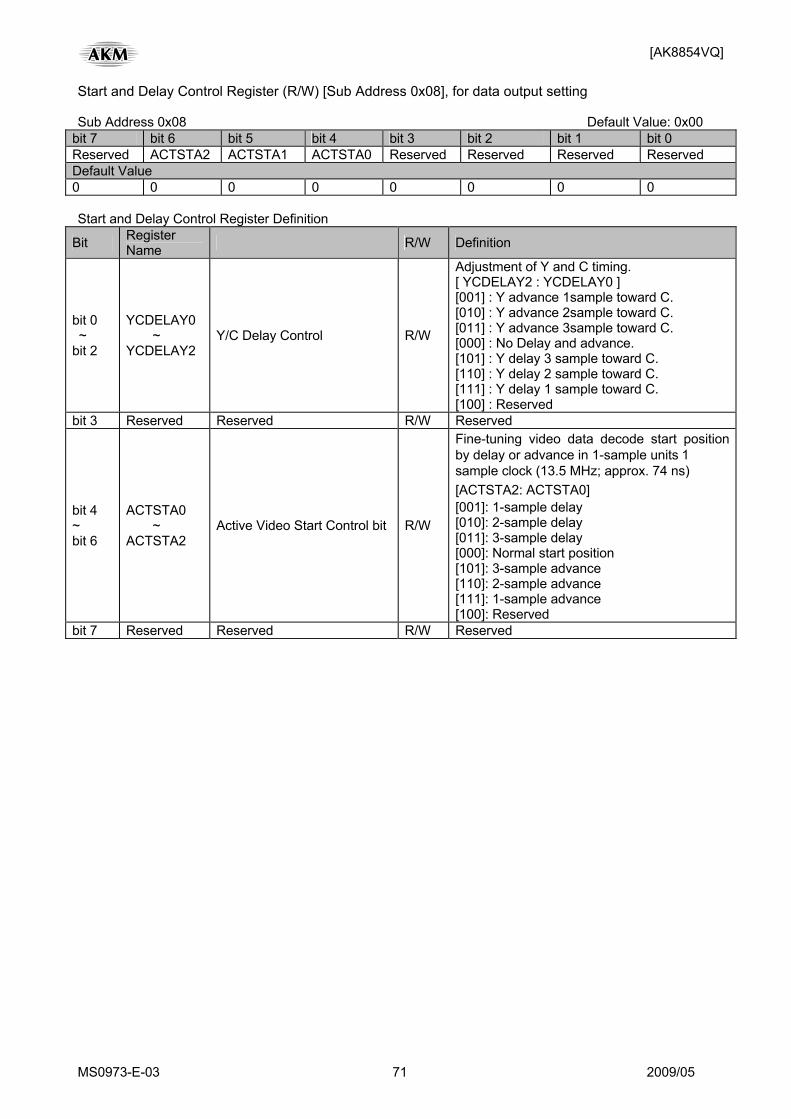
[AK8854VQ]
MS0973-E-03 71 2009/05
Start and Delay Control Register (R/W) [Sub Address 0x08], for data output setting Sub Address 0x08 Default Value: 0x00
bit 7 bit 6 bit 5 bit 4 bit 3 bit 2 bit 1 bit 0 Reserved ACTSTA2 ACTSTA1 ACTSTA0 Reserved Reserved Reserved Reserved Default Value 0 0 0 0 0 0 0 0 Start and Delay Control Register Definition
Bit Register Name R/W Definition
bit 0 ~ bit 2
YCDELAY0 ~ YCDELAY2
Y/C Delay Control R/W
Adjustment of Y and C timing. [ YCDELAY2 : YCDELAY0 ] [001] : Y advance 1sample toward C. [010] : Y advance 2sample toward C. [011] : Y advance 3sample toward C. [000] : No Delay and advance. [101] : Y delay 3 sample toward C. [110] : Y delay 2 sample toward C. [111] : Y delay 1 sample toward C. [100] : Reserved
bit 3 Reserved Reserved R/W Reserved
bit 4 ~ bit 6
ACTSTA0 ~ ACTSTA2
Active Video Start Control bit R/W
Fine-tuning video data decode start position by delay or advance in 1-sample units 1 sample clock (13.5 MHz; approx. 74 ns) [ACTSTA2: ACTSTA0] [001]: 1-sample delay [010]: 2-sample delay [011]: 3-sample delay [000]: Normal start position [101]: 3-sample advance [110]: 2-sample advance [111]: 1-sample advance [100]: Reserved
bit 7 Reserved Reserved R/W Reserved
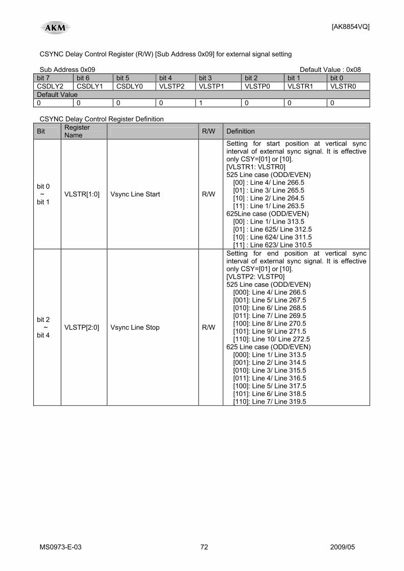
[AK8854VQ]
MS0973-E-03 72 2009/05
CSYNC Delay Control Register (R/W) [Sub Address 0x09] for external signal setting Sub Address 0x09 Default Value : 0x08
bit 7 bit 6 bit 5 bit 4 bit 3 bit 2 bit 1 bit 0 CSDLY2 CSDLY1 CSDLY0 VLSTP2 VLSTP1 VLSTP0 VLSTR1 VLSTR0 Default Value 0 0 0 0 1 0 0 0 CSYNC Delay Control Register Definition
Bit Register Name R/W Definition
bit 0 ~ bit 1
VLSTR[1:0] Vsync Line Start R/W
Setting for start position at vertical sync interval of external sync signal. It is effective only CSY=[01] or [10]. [VLSTR1: VLSTR0] 525 Line case (ODD/EVEN)
[00] : Line 4/ Line 266.5 [01] : Line 3/ Line 265.5 [10] : Line 2/ Line 264.5 [11] : Line 1/ Line 263.5
625Line case (ODD/EVEN) [00] : Line 1/ Line 313.5 [01] : Line 625/ Line 312.5 [10] : Line 624/ Line 311.5 [11] : Line 623/ Line 310.5
bit 2 ~
bit 4 VLSTP[2:0] Vsync Line Stop R/W
Setting for end position at vertical sync interval of external sync signal. It is effective only CSY=[01] or [10]. [VLSTP2: VLSTP0] 525 Line case (ODD/EVEN)
[000]: Line 4/ Line 266.5 [001]: Line 5/ Line 267.5 [010]: Line 6/ Line 268.5 [011]: Line 7/ Line 269.5 [100]: Line 8/ Line 270.5 [101]: Line 9/ Line 271.5 [110]: Line 10/ Line 272.5
625 Line case (ODD/EVEN) [000]: Line 1/ Line 313.5 [001]: Line 2/ Line 314.5 [010]: Line 3/ Line 315.5 [011]: Line 4/ Line 316.5 [100]: Line 5/ Line 317.5 [101]: Line 6/ Line 318.5 [110]: Line 7/ Line 319.5
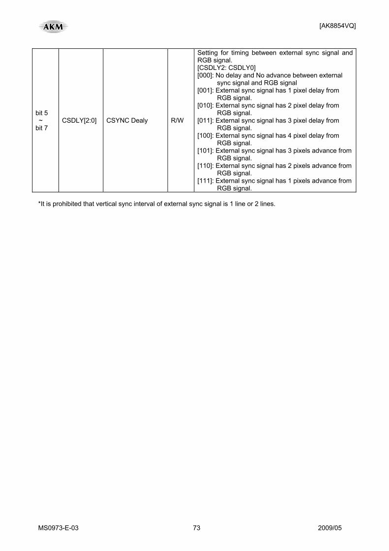
[AK8854VQ]
MS0973-E-03 73 2009/05
bit 5 ~ bit 7
CSDLY[2:0] CSYNC Dealy R/W
Setting for timing between external sync signal and RGB signal. [CSDLY2: CSDLY0] [000]: No delay and No advance between external
sync signal and RGB signal [001]: External sync signal has 1 pixel delay from
RGB signal. [010]: External sync signal has 2 pixel delay from
RGB signal. [011]: External sync signal has 3 pixel delay from
RGB signal. [100]: External sync signal has 4 pixel delay from
RGB signal. [101]: External sync signal has 3 pixels advance from
RGB signal. [110]: External sync signal has 2 pixels advance from
RGB signal. [111]: External sync signal has 1 pixels advance from
RGB signal. *It is prohibited that vertical sync interval of external sync signal is 1 line or 2 lines.

[AK8854VQ]
MS0973-E-03 74 2009/05
AGC & ACC Control Register (R/W) [Sub Address 0x0A], for AGC and ACC setting Sub Address 0x0A Default Value: 0x00
bit 7 bit 6 bit 5 bit 4 bit 3 bit 2 bit 1 bit 0 ACCFRZ ACC1 ACC0 AGCFRZ AGCC1 AGCC0 AGCT1 AGCT0 Default Value 0 0 0 0 0 0 0 0 AGC & ACC Control Register Definition
Bit Register Name R/W Definition
bit 0 ~ bit 1
AGCT0 ~ AGCT1
AGC Time Constant R/W
AGC time constant (T) setting* (if disabled, PGA can be set manually) [AGCT1: AGCT0] [00]: Disable [01]: Fast [T = 1 field] [10]: Middle [T = 7 fields] [11]: Slow [T = 29 fields ]
bit 2 ~ bit 3
AGCC0 ~ AGCC1
AGC Coring Control R/W
AGC non-sensing bandwidth (LSB) setting [AGCC1: AGCC0] [00]: ±2 LSB [01]: ±3 LSB [10]: ±4 LSB [11]: No non-sensing band
bit 4 AGCFRZ AGC Freeze R/W
AGC freeze function (ON/OFF) setting (AGC set values are saved during freeze) [0]: Non-frozen [1]: Frozen
bit 5 ~ bit 6
ACC0 ~ ACC1
ACC Time Constant R/W
ACC time constant (T) setting [ACCT1: ACCT0] [00]: Disable [01]: Fast [T = 2Fields] [10]: Middle [T =8Fields] [11]: Slow [T = 30Fields]
bit 7 ACCFRZ ACC Freeze R/W
ACC freeze function (ON/OFF) setting (ACC set values are saved during freeze) [0] : Non-frozen [1] : Frozen
AGCT must be set “disable” when sync signal is H/VSYNC or CSYNC at RGB input.
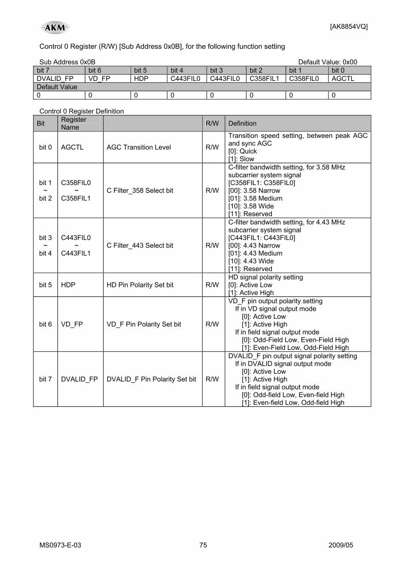
[AK8854VQ]
MS0973-E-03 75 2009/05
Control 0 Register (R/W) [Sub Address 0x0B], for the following function setting Sub Address 0x0B Default Value: 0x00
bit 7 bit 6 bit 5 bit 4 bit 3 bit 2 bit 1 bit 0 DVALID_FP VD_FP HDP C443FIL0 C443FIL0 C358FIL1 C358FIL0 AGCTL Default Value 0 0 0 0 0 0 0 0 Control 0 Register Definition
Bit Register Name R/W Definition
bit 0 AGCTL AGC Transition Level R/W
Transition speed setting, between peak AGC and sync AGC [0]: Quick [1]: Slow
bit 1 ~
bit 2
C358FIL0 ~
C358FIL1 C Filter_358 Select bit R/W
C-filter bandwidth setting, for 3.58 MHz subcarrier system signal [C358FIL1: C358FIL0] [00]: 3.58 Narrow [01]: 3.58 Medium [10]: 3.58 Wide [11]: Reserved
bit 3 ~
bit 4
C443FIL0 ~
C443FIL1 C Filter_443 Select bit R/W
C-filter bandwidth setting, for 4.43 MHz subcarrier system signal [C443FIL1: C443FIL0] [00]: 4.43 Narrow [01]: 4.43 Medium [10]: 4.43 Wide [11]: Reserved
bit 5 HDP HD Pin Polarity Set bit R/WHD signal polarity setting [0]: Active Low [1]: Active High
bit 6 VD_FP VD_F Pin Polarity Set bit R/W
VD_F pin output polarity setting If in VD signal output mode
[0]: Active Low [1]: Active High
If in field signal output mode [0]: Odd-Field Low, Even-Field High [1]: Even-Field Low, Odd-Field High
bit 7 DVALID_FP DVALID_F Pin Polarity Set bit R/W
DVALID_F pin output signal polarity setting If in DVALID signal output mode [0]: Active Low [1]: Active High If in field signal output mode [0]: Odd-field Low, Even-field High [1]: Even-field Low, Odd-field High
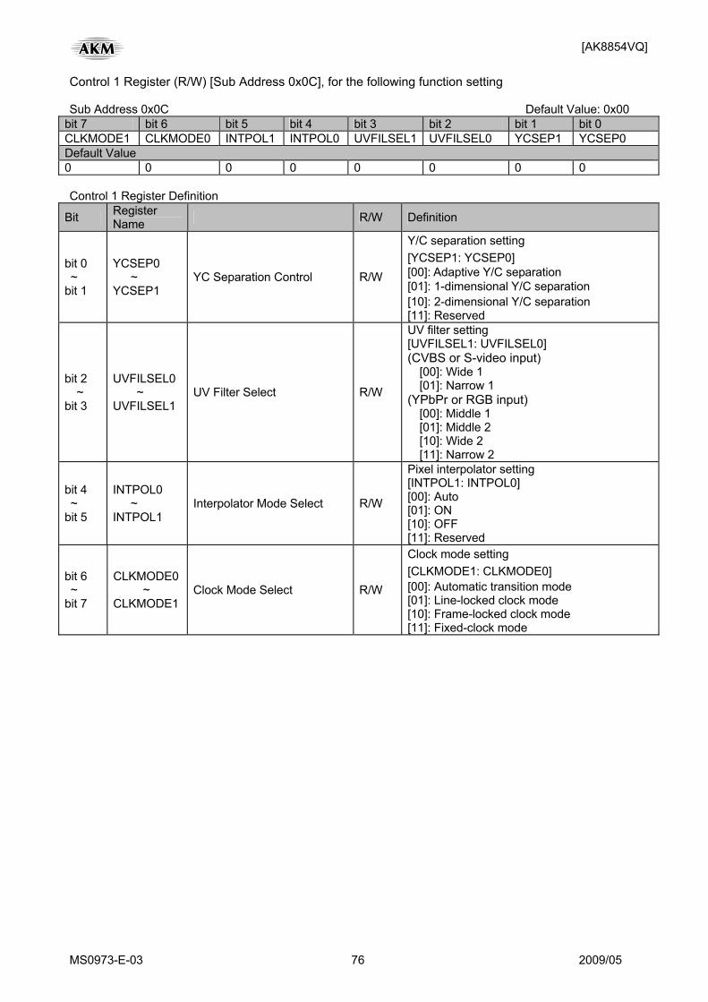
[AK8854VQ]
MS0973-E-03 76 2009/05
Control 1 Register (R/W) [Sub Address 0x0C], for the following function setting Sub Address 0x0C Default Value: 0x00
bit 7 bit 6 bit 5 bit 4 bit 3 bit 2 bit 1 bit 0 CLKMODE1 CLKMODE0 INTPOL1 INTPOL0 UVFILSEL1 UVFILSEL0 YCSEP1 YCSEP0 Default Value 0 0 0 0 0 0 0 0 Control 1 Register Definition
Bit Register Name R/W Definition
bit 0 ~ bit 1
YCSEP0 ~ YCSEP1
YC Separation Control R/W
Y/C separation setting [YCSEP1: YCSEP0] [00]: Adaptive Y/C separation [01]: 1-dimensional Y/C separation [10]: 2-dimensional Y/C separation [11]: Reserved
bit 2 ~
bit 3
UVFILSEL0 ~
UVFILSEL1 UV Filter Select R/W
UV filter setting [UVFILSEL1: UVFILSEL0] (CVBS or S-video input)
[00]: Wide 1 [01]: Narrow 1
(YPbPr or RGB input) [00]: Middle 1 [01]: Middle 2 [10]: Wide 2 [11]: Narrow 2
bit 4 ~ bit 5
INTPOL0 ~ INTPOL1
Interpolator Mode Select R/W
Pixel interpolator setting [INTPOL1: INTPOL0] [00]: Auto [01]: ON [10]: OFF [11]: Reserved
bit 6 ~ bit 7
CLKMODE0 ~ CLKMODE1
Clock Mode Select R/W
Clock mode setting [CLKMODE1: CLKMODE0] [00]: Automatic transition mode [01]: Line-locked clock mode [10]: Frame-locked clock mode [11]: Fixed-clock mode
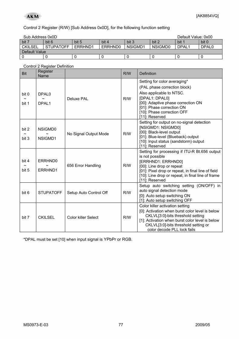
[AK8854VQ]
MS0973-E-03 77 2009/05
Control 2 Register (R/W) [Sub Address 0x0D], for the following function setting Sub Address 0x0D Default Value: 0x00
bit 7 bit 6 bit 5 bit 4 bit 3 bit 2 bit 1 bit 0 CKILSEL STUPATOFF ERRHND1 ERRHND0 NSIGMD1 NSIGMD0 DPAL1 DPAL0 Default Value 0 0 0 0 0 0 0 0 Control 2 Register Definition
Bit Register Name R/W Definition
bit 0 ~ bit 1
DPAL0 ~ DPAL1
Deluxe PAL R/W
Setting for color averaging* (PAL phase correction block) Also applicable to NTSC. [DPAL1: DPAL0] [00]: Adaptive phase correction ON [01]: Phase correction ON [10]: Phase correction OFF [11]: Reserved
bit 2 ~ bit 3
NSIGMD0 ~ NSIGMD1
No Signal Output Mode R/W
Setting for output on no-signal detection [NSIGMD1: NSIGMD0] [00]: Black-level output [01]: Blue-level (Blueback) output [10]: Input status (sandstorm) output [11]: Reserved
bit 4 ~ bit 5
ERRHND0 ~ ERRHND1
656 Error Handling R/W
Setting for processing if ITU-R Bt.656 output is not possible [ERRHND1: ERRHND0] [00]: Line drop or repeat [01]: Pixel drop or repeat, in final line of field [10]: Line drop or repeat, in final line of frame[11]: Reserved
bit 6 STUPATOFF Setup Auto Control Off R/W
Setup auto switching setting (ON/OFF) in auto signal detection mode [0]: Auto setup switching ON [1]: Auto setup switching OFF
bit 7 CKILSEL Color killer Select R/W
Color killer activation setting [0]: Activation when burst color level is below CKLVL[3:0]-bits threshold setting [1]: Activation when burst color level is below CKLVL[3:0]-bits threshold setting or
color decode PLL lock fails *DPAL must be set [10] when input signal is YPbPr or RGB.
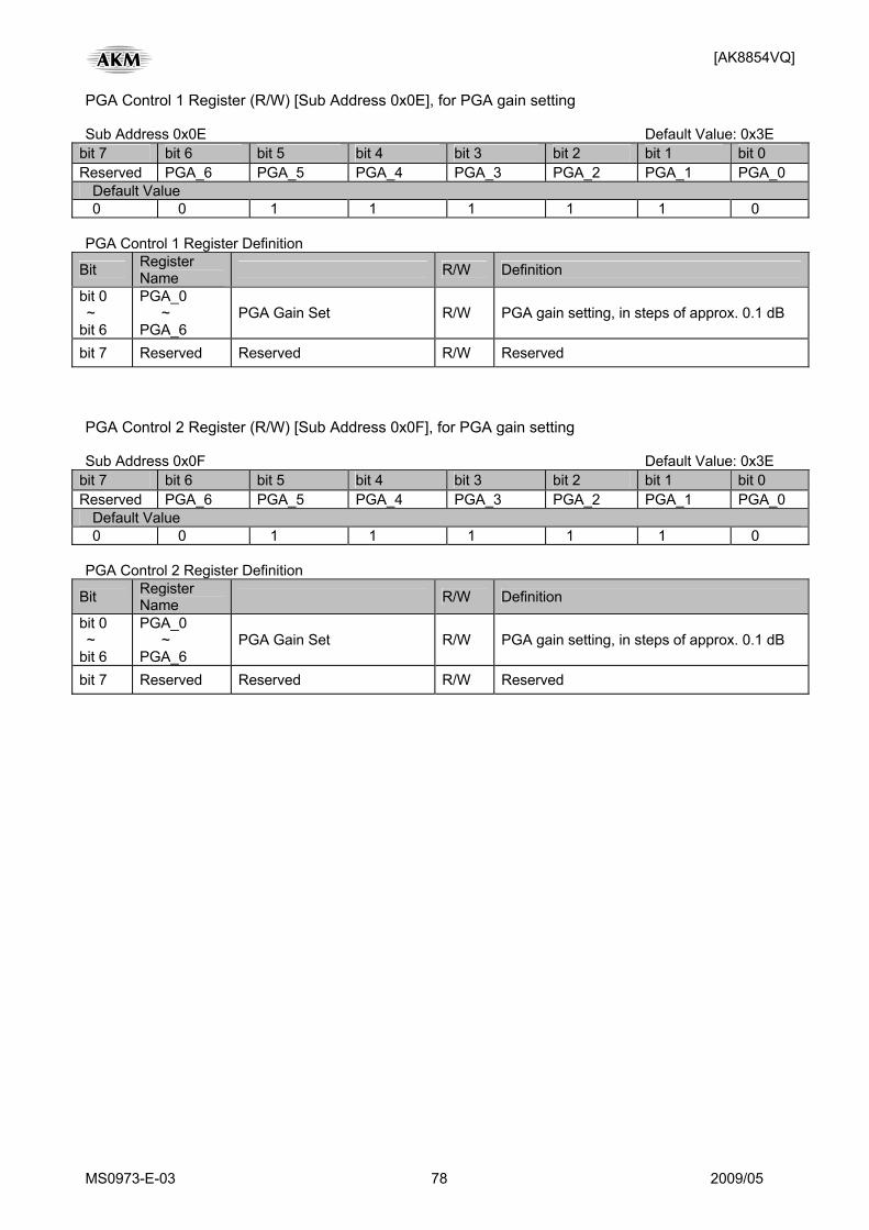
[AK8854VQ]
MS0973-E-03 78 2009/05
PGA Control 1 Register (R/W) [Sub Address 0x0E], for PGA gain setting Sub Address 0x0E Default Value: 0x3E
bit 7 bit 6 bit 5 bit 4 bit 3 bit 2 bit 1 bit 0 Reserved PGA_6 PGA_5 PGA_4 PGA_3 PGA_2 PGA_1 PGA_0
Default Value 0 0 1 1 1 1 1 0
PGA Control 1 Register Definition
Bit Register Name R/W Definition
bit 0 ~ bit 6
PGA_0 ~ PGA_6
PGA Gain Set R/W PGA gain setting, in steps of approx. 0.1 dB
bit 7 Reserved Reserved R/W Reserved PGA Control 2 Register (R/W) [Sub Address 0x0F], for PGA gain setting Sub Address 0x0F Default Value: 0x3E
bit 7 bit 6 bit 5 bit 4 bit 3 bit 2 bit 1 bit 0 Reserved PGA_6 PGA_5 PGA_4 PGA_3 PGA_2 PGA_1 PGA_0
Default Value 0 0 1 1 1 1 1 0
PGA Control 2 Register Definition
Bit Register Name R/W Definition
bit 0 ~ bit 6
PGA_0 ~ PGA_6
PGA Gain Set R/W PGA gain setting, in steps of approx. 0.1 dB
bit 7 Reserved Reserved R/W Reserved
[AK8854VQ]
MS0973-E-03 79 2009/05
Pedestal Level Control Register (R/W) [Sub Address 0x10], for pedestal level adjustment setting Sub Address 0x10 Default Value: 0x00
bit 7 bit 6 bit 5 bit 4 bit 3 bit 2 bit 1 bit 0 DPCC1 DPCC0 DPCT1 DPCT0 BKLVL3 BKLVL2 BKLVL1 BKLVL0 Default Value 0 0 0 0 0 0 0 0 Pedestal Level Control Register Definition
Bit Register Name R/W Definition
bit 0 ~ bit 3
BKLVL0 ~ BKLVL3
Black Level R/W
Setting for change from current pedestal level by adding to or subtracting from black level [BKLVL3: BKLVL0] [0001]: Add 1 [0010]: Add 2 [0011]: Add 3 [0100]: Add 4 [0101]: Add 5 [0110]: Add 6 [0111]: Add 7 [0000]: Default [1000]: Subtract 8 [1001]: Subtract 7 [1010]: Subtract 6 [1011]: Subtract 5 [1100]: Subtract 4 [1101]: Subtract 3 [1110]: Subtract 2 [1111]: Subtract 1
bit 4 ~ bit 5
DPCT0 ~ DPCT1
Digital Pedestal Clamp Control R/W
Time-constant setting for digital pedestal clamp [DPCT1: DPCT0] [00]: Fast [01]: Middle [10]: Slow [11]: Disable
bit 6 ~ bit 7
DPCC0 ~ DPCC1
Digital Pedestal Clamp Coring Control R/W
Non-sensing bandwidth setting for digital pedestal clamp [DPCC1: DPCC0] [00]: ±1bit [01]: ±2bits [10]: ±3bits [11]: No non-sensing band
[AK8854VQ]
MS0973-E-03 80 2009/05
Color Killer Control Register (R/W) [Sub Address 0x11], for color killer setting Sub Address 0x11 Default Value: 0x08
bit 7 bit 6 bit 5 bit 4 bit 3 bit 2 bit 1 bit 0 COLKILL CONTSEL CKSCM1 CKSCM0 CKLVL3 CKLVL2 CKLVL1 CKLVL0 Default Value 0 0 0 0 1 0 0 0 Color Killer Control Register Definition
Bit Register Name R/W Definition
bit 0 ~ bit 3
CKLVL0 ~ CKLVL3
Color Killer Level Control R/W Burst level setting for color killer activation Default value, approx. −23 dB
bit 4 ~ bit 5
CKSCM0 ~ CKSCM1
Color Killer Level for SECAM R/W Burst level setting for color killer activation in SECAM mode Adds 2 bits to CKLVL[3:0]
bit 6 CONTSEL Contrast Select bit R/W Contrast selector [0]: toward luminance of 128 [1]: toward luminance of 0
bit 7 COLKILL Color killer Set R/W Color killer ON/OFF setting [0]: Enable [1]: Disable
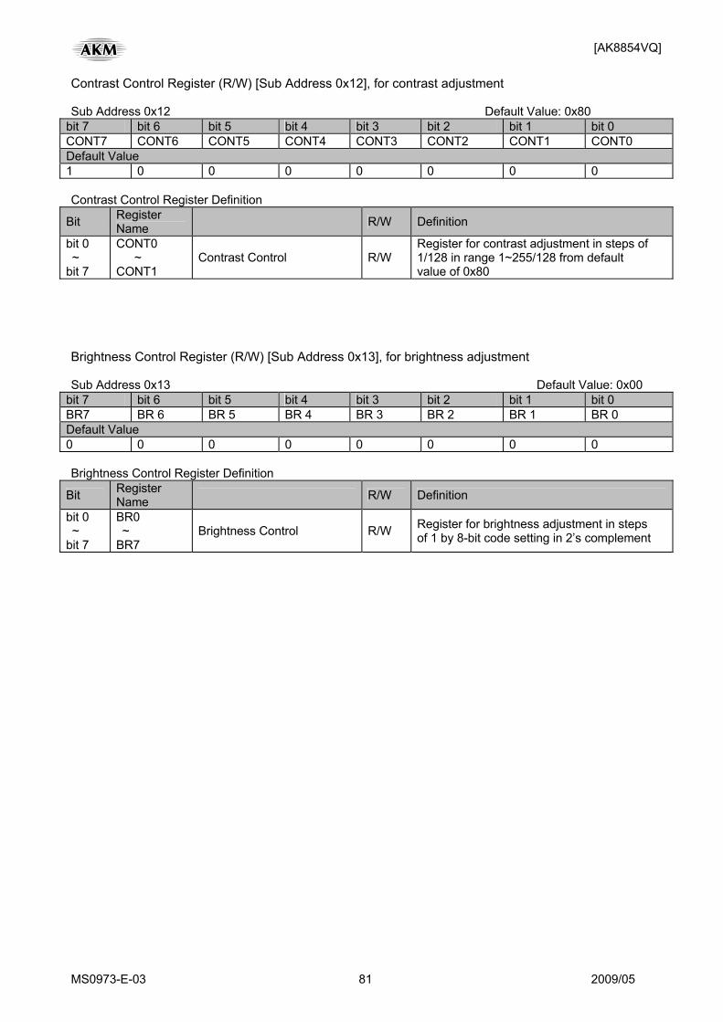
[AK8854VQ]
MS0973-E-03 81 2009/05
Contrast Control Register (R/W) [Sub Address 0x12], for contrast adjustment Sub Address 0x12 Default Value: 0x80
bit 7 bit 6 bit 5 bit 4 bit 3 bit 2 bit 1 bit 0 CONT7 CONT6 CONT5 CONT4 CONT3 CONT2 CONT1 CONT0 Default Value 1 0 0 0 0 0 0 0 Contrast Control Register Definition
Bit Register Name R/W Definition
bit 0 ~ bit 7
CONT0 ~ CONT1
Contrast Control R/W Register for contrast adjustment in steps of 1/128 in range 1~255/128 from default value of 0x80
Brightness Control Register (R/W) [Sub Address 0x13], for brightness adjustment Sub Address 0x13 Default Value: 0x00
bit 7 bit 6 bit 5 bit 4 bit 3 bit 2 bit 1 bit 0 BR7 BR 6 BR 5 BR 4 BR 3 BR 2 BR 1 BR 0 Default Value 0 0 0 0 0 0 0 0 Brightness Control Register Definition
Bit Register Name R/W Definition
bit 0 ~ bit 7
BR0 ~ BR7
Brightness Control R/W Register for brightness adjustment in steps of 1 by 8-bit code setting in 2’s complement
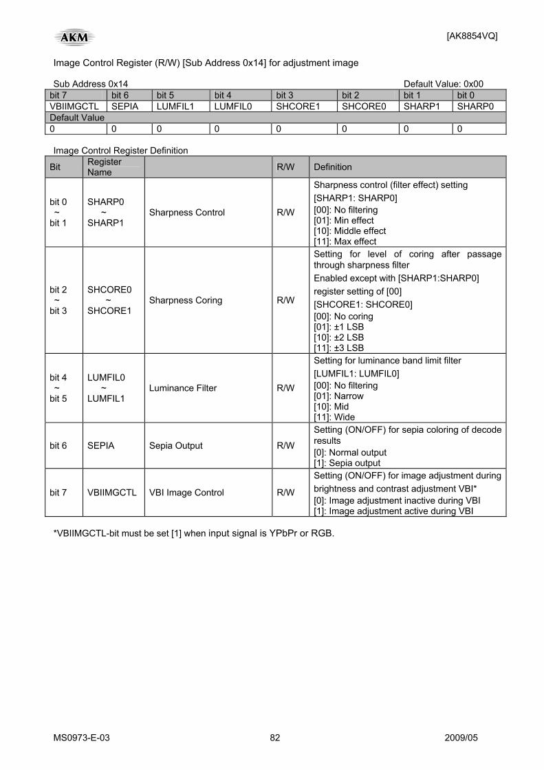
[AK8854VQ]
MS0973-E-03 82 2009/05
Image Control Register (R/W) [Sub Address 0x14] for adjustment image Sub Address 0x14 Default Value: 0x00
bit 7 bit 6 bit 5 bit 4 bit 3 bit 2 bit 1 bit 0 VBIIMGCTL SEPIA LUMFIL1 LUMFIL0 SHCORE1 SHCORE0 SHARP1 SHARP0 Default Value 0 0 0 0 0 0 0 0 Image Control Register Definition
Bit Register Name R/W Definition
bit 0 ~ bit 1
SHARP0 ~ SHARP1
Sharpness Control R/W
Sharpness control (filter effect) setting [SHARP1: SHARP0] [00]: No filtering [01]: Min effect [10]: Middle effect [11]: Max effect
bit 2 ~ bit 3
SHCORE0 ~ SHCORE1
Sharpness Coring R/W
Setting for level of coring after passage through sharpness filter Enabled except with [SHARP1:SHARP0] register setting of [00] [SHCORE1: SHCORE0] [00]: No coring [01]: ±1 LSB [10]: ±2 LSB [11]: ±3 LSB
bit 4 ~ bit 5
LUMFIL0 ~ LUMFIL1
Luminance Filter R/W
Setting for luminance band limit filter [LUMFIL1: LUMFIL0] [00]: No filtering [01]: Narrow [10]: Mid [11]: Wide
bit 6 SEPIA Sepia Output R/W
Setting (ON/OFF) for sepia coloring of decode results [0]: Normal output [1]: Sepia output
bit 7 VBIIMGCTL VBI Image Control R/W
Setting (ON/OFF) for image adjustment duringbrightness and contrast adjustment VBI* [0]: Image adjustment inactive during VBI [1]: Image adjustment active during VBI
*VBIIMGCTL-bit must be set [1] when input signal is YPbPr or RGB.

[AK8854VQ]
MS0973-E-03 83 2009/05
Saturation Control Register (R/W) [Sub Address 0x15], for saturation or U tone level adjustment Sub Address 0x15 Default Value: 0x80
bit 7 bit 6 bit 5 bit 4 bit 3 bit 2 bit 1 bit 0 SAT 7 SAT 6 SAT 5 SAT 4 SAT 3 SAT 2 SAT 1 SAT 0 UTONE7 UTONE6 UTONE5 UTONE4 UTONE3 UTONE2 UTONE1 UTONE0 Default Value 1 0 0 0 0 0 0 0 Saturation Control Register Definition
Bit Register Name R/W Definition
SAT0 ~ SAT7
Saturation Control R/W Register for saturation level adjustment in steps of 1/128 in range 1~255/128 from default value of 0x80 (CVBS or S-video input)bit 0
~ bit 7 UTONE0
~ UTONE7
U Tone Control R/W Register for U tone level adjustment in steps of 1/128 in range 1~255/128 from default value of 0x80 (YPbPr or RGB input)
V Tone Control Register (R/W) [Sub Address 0x16] for V tone level adjustment Sub Address 0x16 Default Value : 0x80
bit 7 bit 6 bit 5 bit 4 bit 3 bit 2 bit 1 bit 0 VTONE7 VTONE6 VTONE5 VTONE4 VTONE3 VTONE2 VTONE1 VTONE0 Default Value 1 0 0 0 0 0 0 0 Saturation Control Register Definition
Bit Register Name R/W Definition
bit 0 ~ bit 7
VTONE0 ~
VTONE7 V Tone Control R/W
Register for V tone level adjustment in steps of 1/128 in range 1~255/128 from default value of 0x80 (YPbPr or RGB input)
HUE Control Register (R/W) [Sub Address 0x17], for hue adjustment Sub Address 0x17 Default Value: 0x00
bit 7 bit 6 bit 5 bit 4 bit 3 bit 2 bit 1 bit 0 HUE 7 HUE 6 HUE 5 HUE 4 HUE 3 HUE 2 HUE 1 HUE 0 Default Value 0 0 0 0 0 0 0 0 HUE Control Register Definition
Bit Register Name R/W Definition
bit 0 ~ bit 7
HUE0 ~ HUE7
HUE Control R/W Register for hue adjustment in steps of 1/128 in range ±45° in 2’s complement
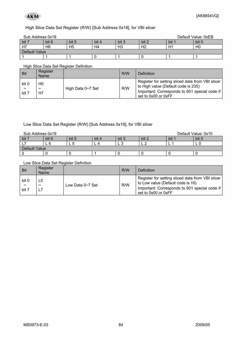
[AK8854VQ]
MS0973-E-03 84 2009/05
High Slice Data Set Register (R/W) [Sub Address 0x18], for VBI slicer Sub Address 0x18 Default Value: 0xEB
bit 7 bit 6 bit 5 bit 4 bit 3 bit 2 bit 1 bit 0 H7 H6 H5 H4 H3 H2 H1 H0 Default Value 1 1 1 0 1 0 1 1 High Slice Data Set Register Definition
Bit Register Name R/W Definition
bit 0 ~ bit 7
H0 ~ H7
High Data 0~7 Set R/W
Register for setting sliced data from VBI slicer to High value (Default code is 235) Important: Corresponds to 601 special code if set to 0x00 or 0xFF
Low Slice Data Set Register (R/W) [Sub Address 0x19], for VBI slicer Sub Address 0x19 Default Value: 0x10
bit 7 bit 6 bit 5 bit 4 bit 3 bit 2 bit 1 bit 0 L7 L 6 L 5 L 4 L 3 L 2 L 1 L 0 Default Value 0 0 0 1 0 0 0 0 Low Slice Data Set Register Definition
Bit Register Name R/W Definition
bit 0 ~ bit 7
L0 ~ L7
Low Data 0~7 Set R/W
Register for setting sliced data from VBI slicer to Low value (Default code is 16) Important: Corresponds to 601 special code if set to 0x00 or 0xFF
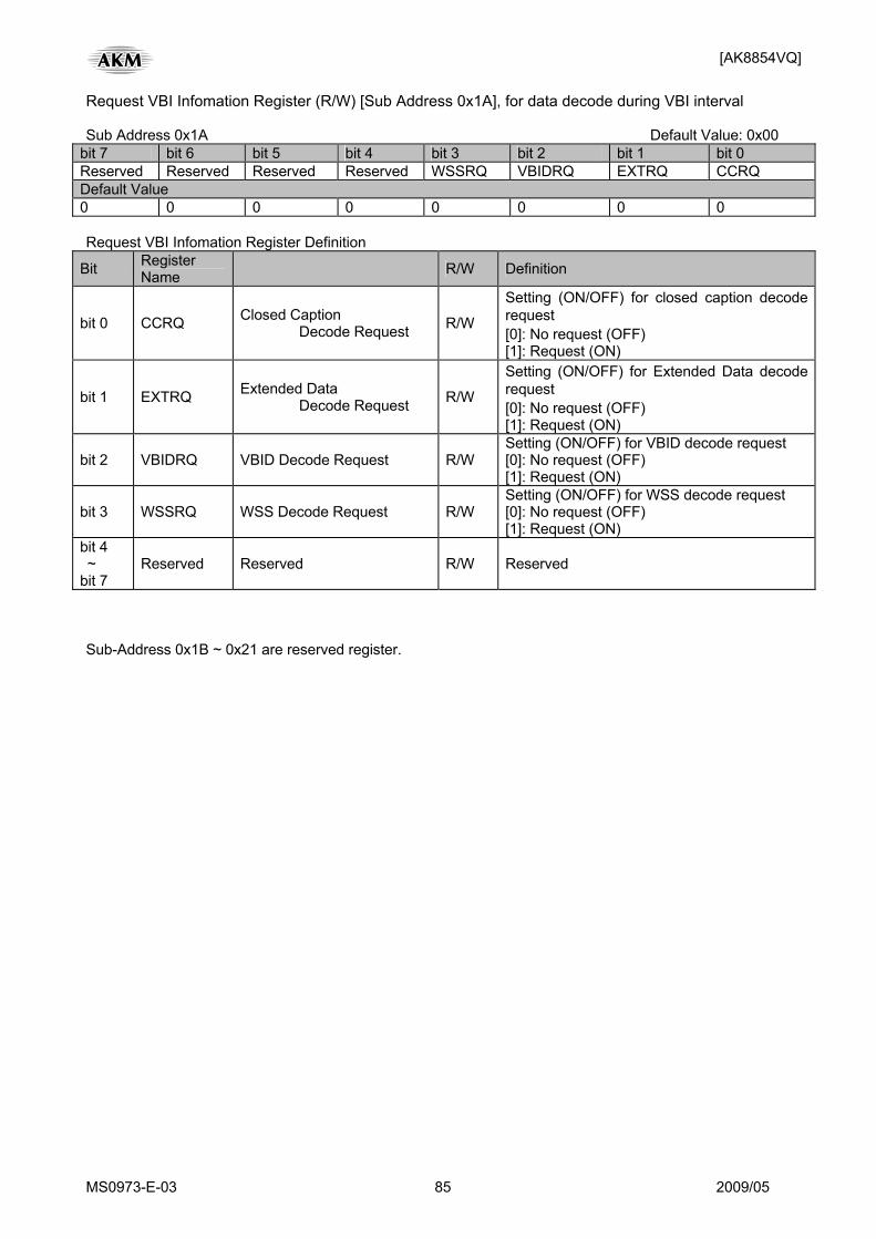
[AK8854VQ]
MS0973-E-03 85 2009/05
Request VBI Infomation Register (R/W) [Sub Address 0x1A], for data decode during VBI interval Sub Address 0x1A Default Value: 0x00
bit 7 bit 6 bit 5 bit 4 bit 3 bit 2 bit 1 bit 0 Reserved Reserved Reserved Reserved WSSRQ VBIDRQ EXTRQ CCRQ Default Value 0 0 0 0 0 0 0 0 Request VBI Infomation Register Definition
Bit Register Name R/W Definition
bit 0 CCRQ Closed Caption Decode Request R/W
Setting (ON/OFF) for closed caption decode request [0]: No request (OFF) [1]: Request (ON)
bit 1 EXTRQ Extended Data Decode Request R/W
Setting (ON/OFF) for Extended Data decode request [0]: No request (OFF) [1]: Request (ON)
bit 2 VBIDRQ VBID Decode Request R/W Setting (ON/OFF) for VBID decode request [0]: No request (OFF) [1]: Request (ON)
bit 3 WSSRQ WSS Decode Request R/W Setting (ON/OFF) for WSS decode request [0]: No request (OFF) [1]: Request (ON)
bit 4 ~ bit 7
Reserved Reserved R/W Reserved
Sub-Address 0x1B ~ 0x21 are reserved register.
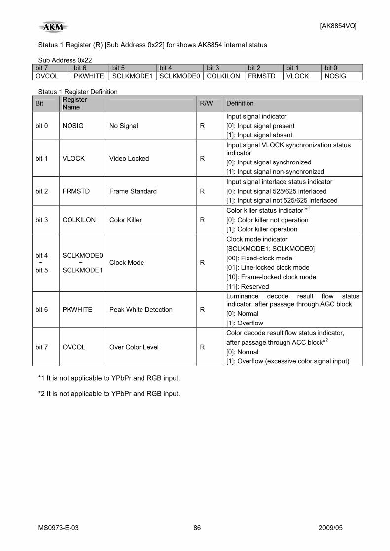
[AK8854VQ]
MS0973-E-03 86 2009/05
Status 1 Register (R) [Sub Address 0x22] for shows AK8854 internal status Sub Address 0x22
bit 7 bit 6 bit 5 bit 4 bit 3 bit 2 bit 1 bit 0 OVCOL PKWHITE SCLKMODE1 SCLKMODE0 COLKILON FRMSTD VLOCK NOSIG Status 1 Register Definition
Bit Register Name R/W Definition
bit 0 NOSIG No Signal R Input signal indicator [0]: Input signal present [1]: Input signal absent
bit 1 VLOCK Video Locked R
Input signal VLOCK synchronization status indicator [0]: Input signal synchronized [1]: Input signal non-synchronized
bit 2 FRMSTD Frame Standard R Input signal interlace status indicator [0]: Input signal 525/625 interlaced [1]: Input signal not 525/625 interlaced
bit 3 COLKILON Color Killer R Color killer status indicator *1 [0]: Color killer not operation [1]: Color killer operation
bit 4 ~ bit 5
SCLKMODE0 ~ SCLKMODE1
Clock Mode R
Clock mode indicator [SCLKMODE1: SCLKMODE0] [00]: Fixed-clock mode [01]: Line-locked clock mode [10]: Frame-locked clock mode [11]: Reserved
bit 6 PKWHITE Peak White Detection R
Luminance decode result flow status indicator, after passage through AGC block [0]: Normal [1]: Overflow
bit 7 OVCOL Over Color Level R
Color decode result flow status indicator, after passage through ACC block*2 [0]: Normal [1]: Overflow (excessive color signal input)
*1 It is not applicable to YPbPr and RGB input. *2 It is not applicable to YPbPr and RGB input.
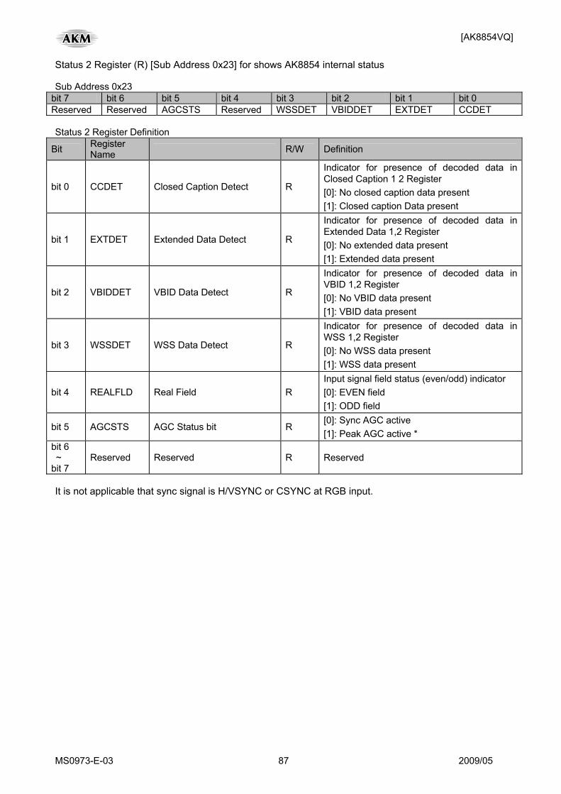
[AK8854VQ]
MS0973-E-03 87 2009/05
Status 2 Register (R) [Sub Address 0x23] for shows AK8854 internal status Sub Address 0x23
bit 7 bit 6 bit 5 bit 4 bit 3 bit 2 bit 1 bit 0 Reserved Reserved AGCSTS Reserved WSSDET VBIDDET EXTDET CCDET Status 2 Register Definition
Bit Register Name R/W Definition
bit 0 CCDET Closed Caption Detect R
Indicator for presence of decoded data in Closed Caption 1 2 Register [0]: No closed caption data present [1]: Closed caption Data present
bit 1 EXTDET Extended Data Detect R
Indicator for presence of decoded data in Extended Data 1,2 Register [0]: No extended data present [1]: Extended data present
bit 2 VBIDDET VBID Data Detect R
Indicator for presence of decoded data in VBID 1,2 Register [0]: No VBID data present [1]: VBID data present
bit 3 WSSDET WSS Data Detect R
Indicator for presence of decoded data in WSS 1,2 Register [0]: No WSS data present [1]: WSS data present
bit 4 REALFLD Real Field R Input signal field status (even/odd) indicator [0]: EVEN field [1]: ODD field
bit 5 AGCSTS AGC Status bit R [0]: Sync AGC active [1]: Peak AGC active *
bit 6 ~ bit 7
Reserved Reserved R Reserved
It is not applicable that sync signal is H/VSYNC or CSYNC at RGB input.
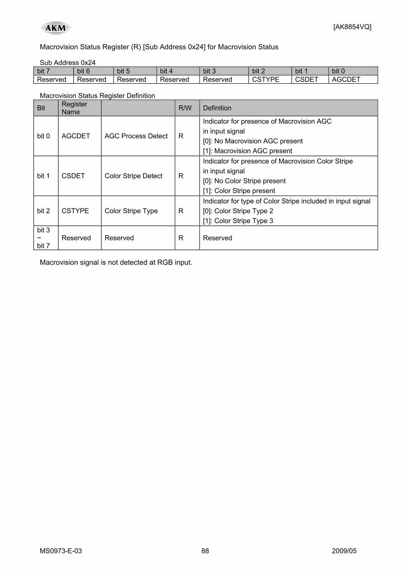
[AK8854VQ]
MS0973-E-03 88 2009/05
Macrovision Status Register (R) [Sub Address 0x24] for Macrovision Status Sub Address 0x24
bit 7 bit 6 bit 5 bit 4 bit 3 bit 2 bit 1 bit 0 Reserved Reserved Reserved Reserved Reserved CSTYPE CSDET AGCDET Macrovision Status Register Definition
Bit Register Name R/W Definition
bit 0 AGCDET AGC Process Detect R
Indicator for presence of Macrovision AGC in input signal [0]: No Macrovision AGC present [1]: Macrovision AGC present
bit 1 CSDET Color Stripe Detect R
Indicator for presence of Macrovision Color Stripe in input signal [0]: No Color Stripe present [1]: Color Stripe present
bit 2 CSTYPE Color Stripe Type R Indicator for type of Color Stripe included in input signal [0]: Color Stripe Type 2 [1]: Color Stripe Type 3
bit 3 ~ bit 7
Reserved Reserved R Reserved
Macrovision signal is not detected at RGB input.
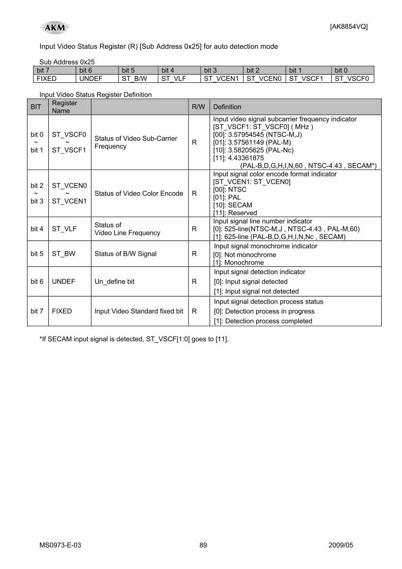
[AK8854VQ]
MS0973-E-03 89 2009/05
Input Video Status Register (R) [Sub Address 0x25] for auto detection mode Sub Address 0x25
bit 7 bit 6 bit 5 bit 4 bit 3 bit 2 bit 1 bit 0 FIXED UNDEF ST_B/W ST_VLF ST_VCEN1 ST_VCEN0 ST_VSCF1 ST_VSCF0 Input Video Status Register Definition
BIT Register Name R/W Definition
bit 0 ~ bit 1
ST_VSCF0 ~ ST_VSCF1
Status of Video Sub-Carrier Frequency R
Input video signal subcarrier frequency indicator [ST_VSCF1: ST_VSCF0] ( MHz ) [00]: 3.57954545 (NTSC-M,J) [01]: 3.57561149 (PAL-M) [10]: 3.58205625 (PAL-Nc) [11]: 4.43361875
(PAL-B,D,G,H,I,N,60 , NTSC-4.43 , SECAM*)
bit 2 ~ bit 3
ST_VCEN0 ~ ST_VCEN1
Status of Video Color Encode R
Input signal color encode format indicator [ST_VCEN1: ST_VCEN0] [00]: NTSC [01]: PAL [10]: SECAM [11]: Reserved
bit 4 ST_VLF Status of Video Line Frequency R
Input signal line number indicator [0]: 525-line(NTSC-M,J , NTSC-4.43 , PAL-M,60) [1]: 625-line (PAL-B,D,G,H,I,N,Nc , SECAM)
bit 5 ST_BW Status of B/W Signal R Input signal monochrome indicator [0]: Not monochrome [1]: Monochrome
bit 6 UNDEF Un_define bit R Input signal detection indicator [0]: Input signal detected [1]: Input signal not detected
bit 7 FIXED Input Video Standard fixed bit R Input signal detection process status [0]: Detection process in progress [1]: Detection process completed
*If SECAM input signal is detected, ST_VSCF[1:0] goes to [11].
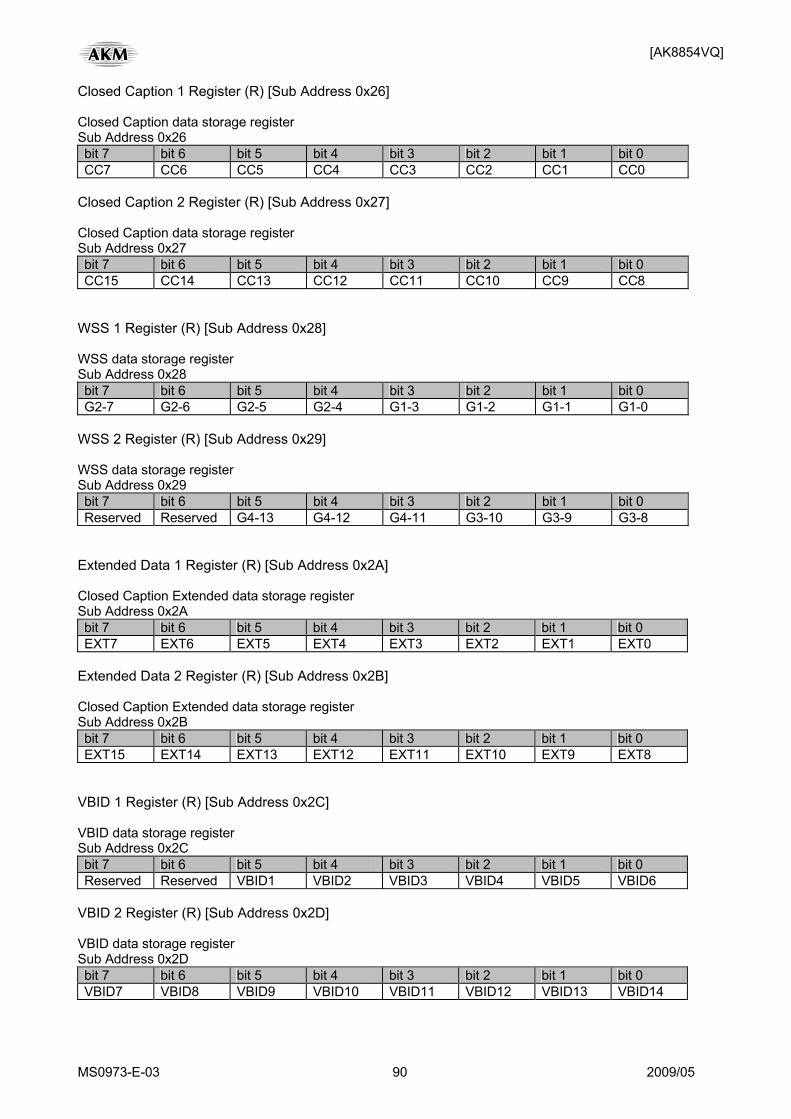
[AK8854VQ]
MS0973-E-03 90 2009/05
Closed Caption 1 Register (R) [Sub Address 0x26] Closed Caption data storage register Sub Address 0x26 bit 7 bit 6 bit 5 bit 4 bit 3 bit 2 bit 1 bit 0 CC7 CC6 CC5 CC4 CC3 CC2 CC1 CC0
Closed Caption 2 Register (R) [Sub Address 0x27] Closed Caption data storage register Sub Address 0x27 bit 7 bit 6 bit 5 bit 4 bit 3 bit 2 bit 1 bit 0 CC15 CC14 CC13 CC12 CC11 CC10 CC9 CC8
WSS 1 Register (R) [Sub Address 0x28] WSS data storage register Sub Address 0x28 bit 7 bit 6 bit 5 bit 4 bit 3 bit 2 bit 1 bit 0 G2-7 G2-6 G2-5 G2-4 G1-3 G1-2 G1-1 G1-0
WSS 2 Register (R) [Sub Address 0x29] WSS data storage register Sub Address 0x29 bit 7 bit 6 bit 5 bit 4 bit 3 bit 2 bit 1 bit 0 Reserved Reserved G4-13 G4-12 G4-11 G3-10 G3-9 G3-8
Extended Data 1 Register (R) [Sub Address 0x2A] Closed Caption Extended data storage register Sub Address 0x2A bit 7 bit 6 bit 5 bit 4 bit 3 bit 2 bit 1 bit 0 EXT7 EXT6 EXT5 EXT4 EXT3 EXT2 EXT1 EXT0
Extended Data 2 Register (R) [Sub Address 0x2B] Closed Caption Extended data storage register Sub Address 0x2B bit 7 bit 6 bit 5 bit 4 bit 3 bit 2 bit 1 bit 0 EXT15 EXT14 EXT13 EXT12 EXT11 EXT10 EXT9 EXT8
VBID 1 Register (R) [Sub Address 0x2C] VBID data storage register Sub Address 0x2C bit 7 bit 6 bit 5 bit 4 bit 3 bit 2 bit 1 bit 0 Reserved Reserved VBID1 VBID2 VBID3 VBID4 VBID5 VBID6
VBID 2 Register (R) [Sub Address 0x2D] VBID data storage register Sub Address 0x2D bit 7 bit 6 bit 5 bit 4 bit 3 bit 2 bit 1 bit 0 VBID7 VBID8 VBID9 VBID10 VBID11 VBID12 VBID13 VBID14
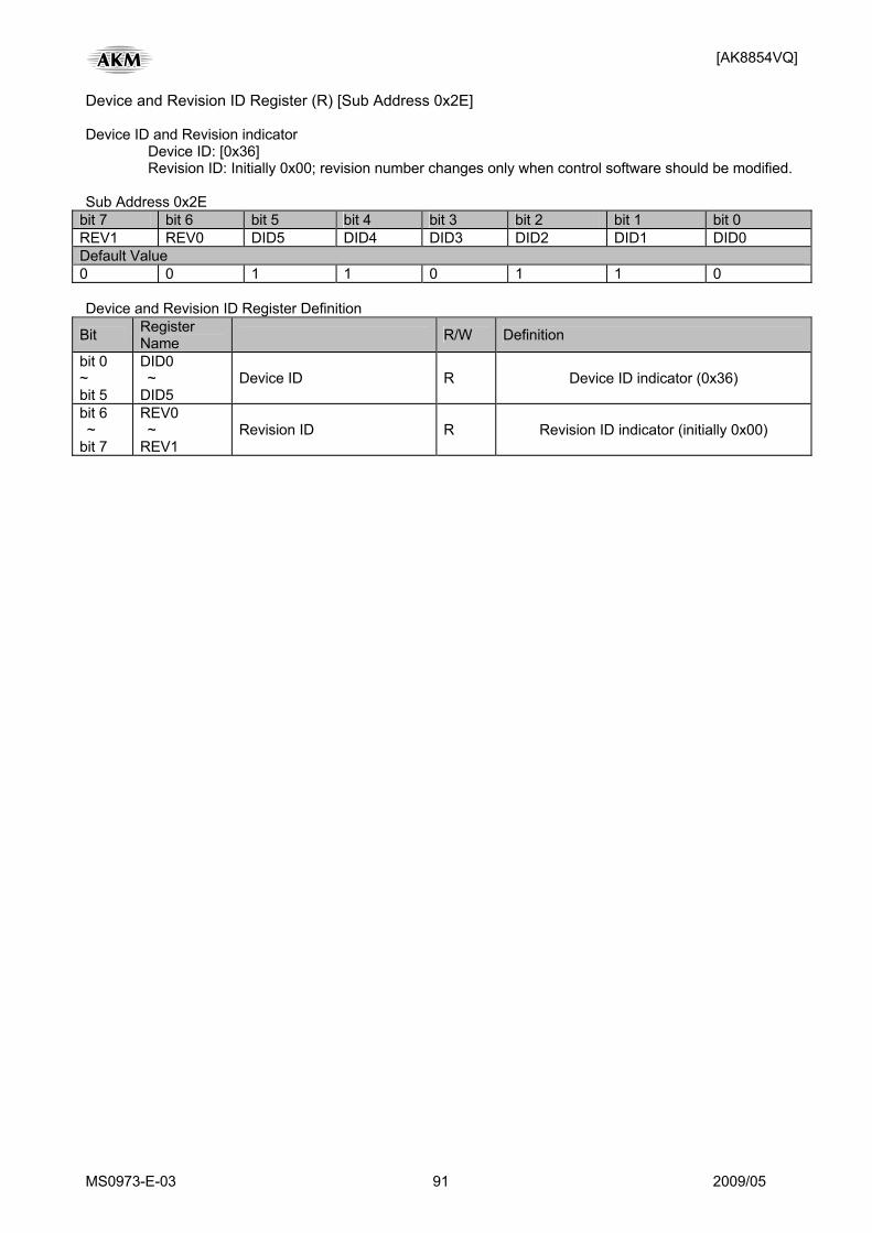
[AK8854VQ]
MS0973-E-03 91 2009/05
Device and Revision ID Register (R) [Sub Address 0x2E] Device ID and Revision indicator Device ID: [0x36] Revision ID: Initially 0x00; revision number changes only when control software should be modified. Sub Address 0x2E
bit 7 bit 6 bit 5 bit 4 bit 3 bit 2 bit 1 bit 0 REV1 REV0 DID5 DID4 DID3 DID2 DID1 DID0 Default Value 0 0 1 1 0 1 1 0 Device and Revision ID Register Definition
Bit Register Name R/W Definition
bit 0 ~ bit 5
DID0 ~ DID5
Device ID R Device ID indicator (0x36)
bit 6 ~ bit 7
REV0 ~ REV1
Revision ID R Revision ID indicator (initially 0x00)
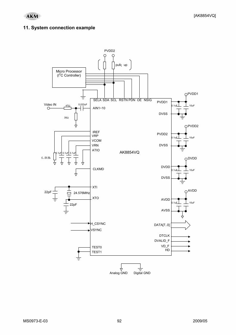
[AK8854VQ]
MS0973-E-03 92 2009/05
11. System connection example
47Ω
30Ω
AIN1~100.033uF
0.1uF 0.1uF
VRPVCOMVRN
SDA SCL RSTN PDN
Micro Processor (I2C Controller)
OE
DATA[7..0]
DTCLKDVALID_F
VD_F HD
Analog GND Digital GND
TEST0
AK8854VQ
IREF
Video IN
PVDD1
PVDD1
TEST1
CLKMD
6.8kΩ
0.1uF 10uF
PVDD2
pull up
0.1uF
XTI
24.576MHz XTO
22pF
22pF
SELA
PVDD2
PVDD2 0.1uF 10uF
DVDD
DVDD 0.1uF 10uF
DVSS
DVSS
ATIODVSS
AVDD
AVDD 0.1uF 10uF
AVSS
H_CSYNC
VSYNC
NSIG
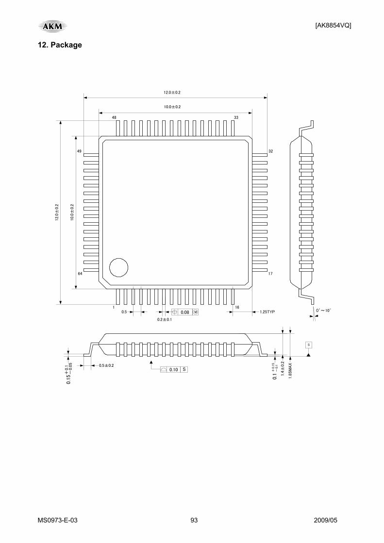
[AK8854VQ]
MS0973-E-03 93 2009/05
12. Package
1 16
17
32
3348
49
64
0.2±0.1
10.0±0.2
12.0±0.2
12.
0±0.
2
10.
0±0.
2
0.5 M0.08 1.25TYP
0.100.5±0.2
1.4±
0.2
1.8
5M
AX
0.1
+ 0.1
5-
0.1
0 ~゜ 10゜
0.15
+ 0.
1-
0.0
5
S
S
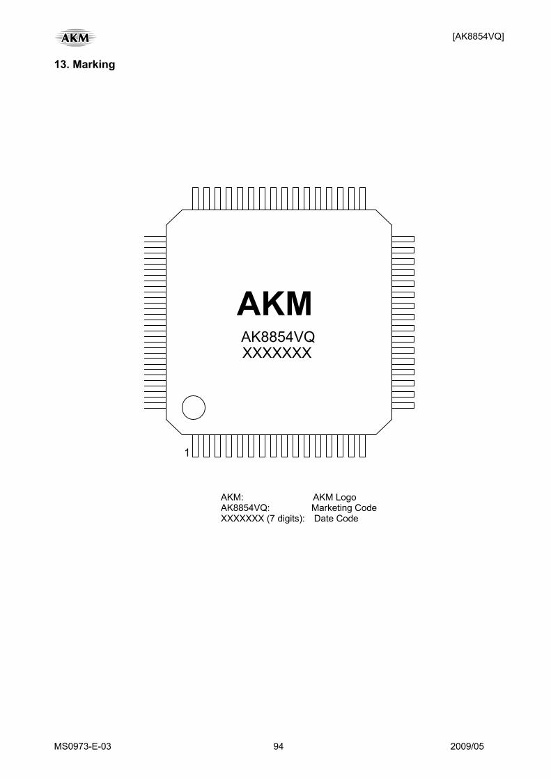
[AK8854VQ]
MS0973-E-03 94 2009/05
13. Marking
1
AKMAK8854VQ XXXXXXX
AKM: AKM Logo AK8854VQ: Marketing Code XXXXXXX (7 digits): Date Code
[AK8854VQ]
MS0973-E-03 95 2009/05
Revision history MS0973-E-00 MS0973-E-01 Page1: Writing mistake "105°C " -- > "85°C " MS0973-E-02 Page18: Parameter Addition "No I2C access" MS0973-E-03 Page1: Addition Notice
[AK8854VQ]
MS0973-E-03 96 2009/05
These products and their specifications are subject to change without notice. Before considering any use or application, consult the Asahi Kasei Microsystems Co., Ltd. (AKM) sales office or authorized distributor concerning their current status. AKM assumes no liability for infringement of any patent, intellectual property, or other
right in the application or use of any information contained herein. Any export of these products, or devices or systems containing them, may require an
export license or other official approval under the law and regulations of the country of export pertaining to customs and tariffs, currency exchange, or strategic materials. AKM products are neither intended nor authorized for use as critical components in any
safety, life support, or other hazard related device or system, and AKM assumes no responsibility relating to any such use, except with the express written consent of the Representative Director of AKM. As used here: (a) A hazard related device or system is one designed or intended for life support or maintenance of safety or for applications in medicine, aerospace, nuclear energy, or other fields, in which its failure to function or perform may reasonably be expected to result in loss of life or in significant injury or damage to person or property. (b) A critical component is one whose failure to function or perform may reasonably be expected to result, whether directly or indirectly, in the loss of the safety or effectiveness of the device or system containing it, and which must therefore meet very high standards of performance and reliability. It is the responsibility of the buyer or distributor of an AKM product who distributes,
disposes of, or otherwise places the product with a third party to notify that party in advance of the above content and conditions, and the buyer or distributor agrees to assume any and all responsibility and liability for and hold AKM harmless from any and all claims arising from the use of said product in the absence of such notification.
IMPORTANT NOTICE