Embed Size (px)
Citation preview

[AK2401]
017003093-E-00 2017/3 1
1. General Description
The AK2401 is a direct conversion transceiver that provides high performance narrow-band radio communication. The receiver block of the AK2401 integrates a LNA, I/Q demodulator, PGA and 24-bit delta-sigma ADC, and realizes both performances of high sensitivity and high tolerance to adjacent channel interference, intermodulation and blocking. Digital filter that is able to support channel selection for multiple radio systems, enabling simple system designing for a radio platform. The AK2401 also integrates a delta-sigma Fractional-N synthesizer that composes a high performance PLL with an external VCO. The transmission block has a DAC and a driver amplifier. The AK2401 is housed in a small QFN package (7mm x 7mm), realizing to downsize wire-less applications.
2. Features
Operating Frequency: 30MHz ~ 1200MHz Power Supply: 2.7 ~ 3.3V (CPVDD, DACVDD: 2.7 ~ 5.5V) Operational Temperature: -40 ~ +85ºC LNA: Gain 15dB, NF 1.2dB, IIP3 +7dBm High Linearity Direct Conversion I/Q Demodulator 24-bit ΔΣ A/D Converter: up to 150kHz Output Sampling Frequency (TCXO=19.2MHz) Band Changeable Digital Filter (Bandwidth can be set arbitrarily) Automatic Gain Control (AGC) function for LNA and PGA Real-time DC Offset Canceller (RDOC) Function RSSI Function: Data read by SPI communication 18-bit ΔΣ Fractional-N PLL Synthesizer Digital Frequency Modulation (FM/FSK) by Frequency Offset Function Fast Lock Function reduces Lock-up Time 12-bit DAC: 200kHz Max. Sampling Frequency, S/N 72dB Transmission Driver Amplifier: −6 ~ +6 dBm Output Local Signal Dividing Circuit (divide by 2 or more is recommended) TCXO Frequency: 18.432MHz / 19.2MHz are recommended Frequency: 52-pin QFN (7×7×0.85mm 0.4 mm pitch)
3. Application
• Narrow Band Radio Communication: 6.25kHz/7.5kHz/12.5kHz/15kHz/20kHz/25kHz/ 50kHz/100kHz/150kHz / etc.
• Modulation Method: FM/2FSK/4FSK/QPSK//4 DQPSK /16QAM/64QAM (Modulation / demodulation needs to be done externally. Modem function is not installed.)
• Analog/Digital Dual Mode Transceiver • Digital Radio System for Industrial Use • Public safety and Community/Emergency Radio System • Convenience Transceiver • Marine/Mobile Communication System • Low power / Telemeter Transmitter • Amateur Radio System
AK2401 Direct Conversion Transceiver

[AK2401]
017003093-E-00 2017/3 2
4. Table of Contents
1. General Description ......................................................................................................................... 1 2. Features........................................................................................................................................... 1 3. Application ....................................................................................................................................... 1 4. Table of Contents ............................................................................................................................ 2 5. Block Diagram and Functions ......................................................................................................... 5
5.1. Block Diagram .............................................................................................................................. 5 5.2. Functions ..................................................................................................................................... 5
6. Pin Configurations and Functions ................................................................................................... 7 6.1. Pin Configurations ....................................................................................................................... 7 6.2. Pin Functions ............................................................................................................................... 8 6.3. Handling of Unused Pins ........................................................................................................... 10
7. Absolute Maximum Ratings........................................................................................................... 11 8. Recommended Operating Conditions ........................................................................................... 11 9. Digital Characteristics .................................................................................................................... 12
9.1. DC Characteristics ..................................................................................................................... 12 9.2. System Reset ............................................................................................................................. 12 9.3. Serial Interface Timing for Register Access .............................................................................. 13 9.4. Serial Interface Timing for Programmable FIR Filter Coefficient Setting .................................. 14 9.5. Serial Interface Timing for ADC Data Readout ......................................................................... 14 9.6. Serial Interface Timing for DAC Data Write ............................................................................... 15
10. Analog Characteristics .................................................................................................................. 16 10.1. Receiving Characteristics ...................................................................................................... 16
10.1.1. LNA ................................................................................................................................. 16 10.1.2. MIXER+PGA+AAF+ADC ................................................................................................ 16 10.1.3. LOCAL BUFFER+LOCAL DIVIDER (RX) ...................................................................... 18 10.1.4. PLL SYNTHESIZER ....................................................................................................... 18 10.1.5. RSSI ................................................................................................................................ 19
10.2. Transmission Characteristics ................................................................................................. 20 10.2.1. DAC+SMF ....................................................................................................................... 20 10.2.2. LOCAL BUFFER+LOCAL DIVIDER(TX)+DRIVER AMP ............................................... 20
10.3. Current Consumption ............................................................................................................. 21 11. Typical Performance Characteristics ............................................................................................ 22 12. Operation Sequence ..................................................................................................................... 22
12.1. Power-up Sequence ............................................................................................................... 22 12.2. Power-up Sequence of PLL Synthesizer ............................................................................... 23 12.3. DC Offset Calibration Sequence ............................................................................................ 24
13. Functional Descriptions ................................................................................................................. 25 13.1. Power Management ............................................................................................................... 25 13.2. Operation Mode Setting ......................................................................................................... 27 13.3. Level Diagram ........................................................................................................................ 28
13.3.1. Level Diagram of Analog Receiving Circuit .................................................................... 28 13.3.2. Level Diagram of Digital Receiving Circuit ..................................................................... 29
13.4. Analog Receiving Circuit (LNA) ............................................................................................. 30 13.5. Analog Receiving Circuit (MIXER, PGA, AAF) ...................................................................... 32
13.5.1. MIXER ............................................................................................................................. 32 13.5.2. Analog Filter Frequency Characteristics......................................................................... 33 13.5.3. Output Path Selection of Analog Baseband Signal ........................................................ 34
13.6. LOCAL BUFFER, LOCAL DIVIDER ...................................................................................... 35 13.6.1. LOCAL BUFFER ............................................................................................................. 35 13.6.2. LOCAL DIVIDER ............................................................................................................. 35 13.6.3. Phase Calibration............................................................................................................ 35
13.7. PLL SYNTHESIZER ............................................................................................................... 38 13.7.1. CHARGE PUMP, LOOP FILTER ................................................................................... 38 13.7.2. Frequency Setting ........................................................................................................... 39 13.7.3. Frequency Offset Adjustment ......................................................................................... 39

[AK2401]
017003093-E-00 2017/3 3
13.7.4. Fast Lock Function.......................................................................................................... 42 13.7.5. Lock Detection ................................................................................................................ 43
13.8. Digital Receiving Circuit (ADC, DIGITAL FILTER, RSSI, AGC, ADC P/S IF) ....................... 45 13.8.1. ADC ................................................................................................................................. 45 13.8.2. Digital Filter Frequency Characteristics .......................................................................... 45 13.8.3. Programmable FIR Filter ................................................................................................ 48 13.8.4. High-Pass Filter .............................................................................................................. 53 13.8.5. Fast Track Mode ............................................................................................................. 55 13.8.6. DC Offset Calibration ...................................................................................................... 57 13.8.7. RDOC Function ............................................................................................................... 59 13.8.8. AGC Function ................................................................................................................. 60 13.8.9. AGC_KEEP Function ...................................................................................................... 64 13.8.10. RSSI Function ................................................................................................................. 66 13.8.11. Output Sampling Rate .................................................................................................... 68 13.8.12. ADC P/S IF ..................................................................................................................... 69
14. Register Map ................................................................................................................................. 70 15. Register Definitions ....................................................................................................................... 73
15.1. <0x01~0x03>FRAC ............................................................................................................... 73 15.2. <0x04~0x06>MOD ................................................................................................................. 73 15.3. <0x07~0x08>INT.................................................................................................................... 73 15.4. <0x09>RDIV ........................................................................................................................... 73 15.5. <0x0A~0x0B>CP.................................................................................................................... 74 15.6. <0x0C>SYNTH ...................................................................................................................... 75 15.7. <0x0D~0x0E>FAST TIME ..................................................................................................... 75 15.8. <0x0F~0x11>FREQ OFFSET1 .............................................................................................. 76 15.9. <0x12>LOCAL ....................................................................................................................... 76 15.10. <0x13>TX ............................................................................................................................... 76 15.11. <0x14>RX .............................................................................................................................. 77 15.12. <0x15~0x16>PGA GAIN ........................................................................................................ 78 15.13. <0x17~0x18>CAL START ..................................................................................................... 79 15.14. <0x19~0x1E>CH_DC OFST .................................................................................................. 80 15.15. <0x1F~0x21, 0x47~048>AGC ............................................................................................... 80 15.16. <0x22>CH FILTER ................................................................................................................. 84 15.17. <0x23>PROG FILTER ........................................................................................................... 84 15.18. <0x24~0x25>HPF .................................................................................................................. 85 15.19. <0x26~0x28, 0x44~0x46>RDOC ........................................................................................... 86 15.20. <0x29~0x2B>FREQ OFFSET2 ............................................................................................. 88 15.21. <0x2C>RSSI .......................................................................................................................... 88 15.22. <0x2D>FIR COEF .................................................................................................................. 89 15.23. <0x2E>PD .............................................................................................................................. 90 15.24. <0x2F~0x30>READ PGA ...................................................................................................... 90 15.25. <0x31~0x36>READ OFST ..................................................................................................... 90 15.26. <0x37~0x39>READ COEF .................................................................................................... 91 15.27. <0x3A>READ RSSI ............................................................................................................... 91 15.28. <0x3B~0x3E>ANA DC OFST ................................................................................................ 91 15.29. <0x3F~0x40>LDCNT ............................................................................................................. 92 15.30. <0x41~0x43>PHASE CAL ..................................................................................................... 92 15.31. <0x49>PRE TESTEN ............................................................................................................. 93 15.32. <0x4A>CH FILTER2 .............................................................................................................. 94 15.33. <0x4B>STATUS ..................................................................................................................... 94 15.34. <0x5F>SOFT RESET ............................................................................................................ 94
16. Recommended External Circuits ................................................................................................... 95 16.1. Recommended External Circuits ........................................................................................... 95 16.2. List of Parts ............................................................................................................................ 95 16.3. Power Supply/Ground Pin ...................................................................................................... 96 16.4. PCB Design ............................................................................................................................ 97 16.5. PCB Layout ............................................................................................................................ 98

[AK2401]
017003093-E-00 2017/3 4
17. LSI Interface Circuit ....................................................................................................................... 99 18. Package ....................................................................................................................................... 101
18.1. Outline Dimensions .............................................................................................................. 101 18.2. Marking ................................................................................................................................. 101
19. Ordering Guide ............................................................................................................................ 102 20. Revision History ........................................................................................................................... 102

[AK2401]
017003093-E-00 2017/3 5
5. Block Diagram and Functions
5.1. Block Diagram
Figure 1. AK2401 Block Diagram
5.2. Functions The AK2401 consists of the Analog Receiving Circuit 1 (LNA), the Analog Receiving Circuit 2 (MIXER, PGA and AAF), the Digital Receiving Circuit (ADC, DIGITAL FILTER, RSSI, AGC and ADC P/S IF), the Local Oscillation Circuit (PLL SYNTHESIZER, LOCAL BUFFER, LOCAL DIVIDER and CLOCK BUFFER), the Transmitting Data Generation Circuit (DAC S/P IF, DAC and SMOOTHING FILTER), the Transmitting Pre-amplifier Circuit (DRIVER AMP), the Reference Voltage Generation Circuit (VREF), the Internal Low Voltage Generation Circuit (LDO) and the Digital Control Circuit (DGITAL CONTROL). Analog Receiving Circuit 1 (LNA: Low Noise Linear Amplifier)
Amplify received RF signal in low noise. An automatic gain controlling (AGC) function that automatically switches operation mode according to the input signal level is implemented to prevent degradation of distortion characteristics in strong input environment. An external matching circuit is needed at input/output of the LNA. An external filter can be added between the LNA and the MIXER blocks depending on the Image suppression characteristic demands.
Analog Receiving Circuit 2 (MIXER, PGA, AAF) The direct conversion type MIXER down coverts RF signal that is amplified by LNA. The MIXER is operated by two local signals with 90 degrees phase difference, and it generates Ich/Qch baseband signal. A matching circuit is necessary at the MIXER input. The PGA (programmable gain amplifier) is composed by a first-order low-pass filter that is able to change the gain by register settings. It amplifies the dynamic range by keeping the input level of the ADC after this block. The PGA has an AGC function that changes PGA gain automatically according to input signal level. The AAF is composed by a third-order low-pass filter (Fc=100kHz). It is an anti-aliasing filter that prevents aliasing at the ADC after this block. An analog filter is composed by the PGA and the AAF reducing blocking signals on ADC input.
AO
UT
_P
AO
UT
_N
LOCALDIVIDER1/(1,2,4,8)
LNA
LNACONT
LN
AO
UT
DE
MIN
MIXER PGA AAF
DIGITAL CONTROL
DC OFFSETCAL
DC OFFSETCAL
VC
OM
_A
D
1/4
LNAIN
DRIVER AMP
RFOUT_N
RFOUT_P
BALUN
BIAS1
BIAS2
VREF2
VREF1
TEST2
+90 0
LO
IN
FRACTIONAL-NPLL SYNTHESIZER
ΔΣMODULATOR
R COUNTER
CP
SW
IN
CP
Z
TC
XO
IN
PHASEFREQUENCYDETECTOR
CHARGEPUMP
N DIVIDER
LOOPFILTER
VCOLPF
VREF
LDO
to power amplifier
from antenna and/or top filter
matching circuit and/or optional BPF
TX
_D
PN
RX
_P
DN
RS
TN
SD
AT
AO
SD
AT
AI
CS
N
SC
LK
LD
AG
C_K
EE
P
AGC(LNA & PGA)
I+
Q+
I-
Q-
RSSI
MCU/DSP
24-bitΔΣ ADC
24-bitΔΣ ADC
LOCALBUFFER
CLOCKBUFFER
DIGITAL FILTER
AD_SDO
AD_SCLK
AD_FS
DA_SDI
DA_SCLK
DA_FS
SMFOUT
TEST1
MCU/DSP
to VCO modulation
ADCP/S IF
DACS/P IF
12-bitDAC
SMF

[AK2401]
017003093-E-00 2017/3 6
Digital Receiving Circuit (ADC, DIGITAL FILTER, RSSI, AGC, ADC P/S IF) The 24-bit delta-sigma A/D converter converts an analog baseband signal that is generated at the analog receiving circuit to a digital baseband signal. The digital filter is composed by a decimation filter and a channel filter for removing adjacent channel interference and blocking. The channel filter is selected from 10 types standard channel filters that have different frequency characteristics and FIR filter that can be set the coefficient arbitrary. The narrowest pass band of the standard channel filters is 2 kHz and the widest is 60 kHz. The output sampling frequency differs depending on the type of selected channel filter, and it will be 150 kHz at maximum when using a 19.2 MHz reference clock. A DC OFFSET CAL block is composed of a real-time DC offset canceller (RDOC) and a DC offset calibrator. It cancels DC offset that is superimposed to a baseband signal. The RSSI outputs a signal-strength level of the DC OFFSET CAL output. It can be confirmed by register read on SPI. The parallel interface for ADC outputs digital baseband signals.
Local Generation Circuit (PLL SYNTHESIZER, LOCAL BUFFER, LOCAL DIVIDER, CLOCK BUFFER) The FRACTIONAL-N PLL is composed by a PLL SYNTHESIZER, external LOOP FILTER and VCO. It generates a local frequency signal by multiplying the reference clock from the TCXOIN pin by “N”, and converts to a local frequency by dividing the signal by “N” (N=1, 2, 4, 8) at LOVAL DIVIDER. At the same time, two local signals that have 90 degree phase difference are generated.
Transmitting Data Generation Circuit (DAC S/P IF, DAC, SMF) The 12-bit DA converter converts a digital baseband signal that is input to a serial/parallel interface for DAC to an analog baseband signal. The SMF (SMOOTHING FILTER) is a low-pass filter (fc=20kHz) that smoothing the DAC output. These circuits are used for generating an audio signal of transmission and connected to voltage control pin of an external VCO. In other case, it is able to be used as a general purpose 12-bit DAC.
Transmitting Pre-amplifier Circuit (DRIVER AMP) This circuit amplifies a signal that is divided by “N” by the LOCAL DIVIDER and outputs. It is assumed to use as a transmitting signal output when modulating the signal directly by an external VCO.
Reference Voltage Generation Circuit (VREF) Generate reference voltage for each block.
Internal Low Voltage Generation Circuit (LDO) Generate a 1.9V power from external 3V power (SYNVDD). This internal power supply is supplied to the digital receiving circuit, the digital control circuit and a part of local oscillation circuit.
Digital Control Circuit (DIGITAL CONTROL) • Register Write/Read by 4-wire Serial Interface
(CSN, SCLK, SDATAI, SDATAO pins) • Hardware Reset Signal Input (RSTN pin) • AGC Function Control Signal Input (AGC_KEEP pin) • PLL Status Output (LD pin) • Power Management by Pins (RX_PDN, TX_PDN pins)

[AK2401]
017003093-E-00 2017/3 7
6. Pin Configurations and Functions
6.1. Pin Configurations
RS
TN
VC
OM
_A
D
AD
VD
D
AD
VS
S
TE
ST
2
AO
UT
_N
AO
UT
_P
RX
VD
D
BIA
S1
LN
AV
DD
LN
AC
ON
T
LN
AIN
VS
S
39
38
37
36
35
33
32
31
30
29
28
27
34
42
40
41
43
44
45
46
47
48
49
50
51
52
26
25
24
23
22
21
20
19
18
17
16
15
14
1
2
3
4
5
6
7
8
9
10
11
12
13
DA
_S
CLK
DV
SS
DA
_S
DI
TE
ST
1
BIA
S2
SM
FO
UT
DA
CV
DD
VR
EF
1
TC
XO
IN
VR
EF
2
SY
NV
SS
SY
NV
DD
CP
VD
D
DEMVDD
VSS
LNAOUT
DEMIN
VSS
LOVDD
RFOUT_N
RFOUT_P
LOIN
LODVDD
CPZ
SWIN
CP
Back Side: Exposed PAD
RX_PDN
TX_PDN
AGC_KEEP
CSN
SDATAI
SCLK
SDATAO
LD
DVDD
AD_SCLK
AD_SDO
AD_FS
DA_FS
Figure 2. Pin Configurations (52-pin QFN0707)

[AK2401]
017003093-E-00 2017/3 8
6.2. Pin Functions AI: Analog Input Pin, AO: Analog Output Pin, DI: Digital Input Pin, DO: Digital Output Pin, P: Power Supply Pin, G: Ground Pin All digital input pins must not be allowed to float.
No. Pin Name Type PD Status Function
1 DA_SCLK DI Hi-Z Serial Data Clock Input for D/A Converter
2 DVSS G - Digital Ground for Interface Circuit.
3 DA_SDI DI Hi-Z D/A Converter Serial Data Input
4 TEST1 DI 100kΩ
Pull down Test Pin. Connect to VSS.
5 BIAS2 AI - Resistance Pin for setting charge pump output current
6 SMFOUT AO Hi-Z Smoothing Filter Output
7 DACVDD P - Analog Power Supply for D/A Converter
8 VREF1 AO - LDO Reference
Connect a capacitor to stabilize LDO reference voltage
9 TCXOIN AI 27kΩ
Pull down Reference Clock Input
10 VREF2 AO - Reference Voltage Pin
Connect a capacitor to stabilize reference voltage.
11 SYNVSS G - Analog Ground for Synthesizer
12 SYNVDD P - Analog Power Supply for Synthesizer
13 CPVDD P - Analog Power Supply for Charge Pump
14 CP AO Hi-Z Charge Pump Output
15 SWIN AI * 1 Connect a resistor for Fast Lock
16 CPZ AI * 1 Connect a capacitor for Loop Filter
17 LODVDD P - Analog Power Supply for Local Divider and Local Buffer
18 LOIN AI 50Ω
Pull down Local Input
19 RFOUT_P AO Hi-Z * 2 Driver Amplifier Positive Output
20 RFOUT_N AO Hi-Z * 2 Driver Amplifier Negative Output
21 LOVDD P - Analog Power Supply for Local Amplifier and Driver Amplifier
22 VSS G * 3 Ground
23 DEMIN AI H-Z MIXER Input
24 DEMVDD P - Analog Power Supply for MIXER
25 LNAOUT AO Hi-Z * 2 LNA Output
26 VSS G * 3 Ground
27 VSS G * 3 Ground
28 LNAIN AI 100kΩ
Pull down LNA Input
29 LNACONT AI Hi-Z LNA Matching Adjustment Pin
30 LNAVDD P - Analog Power Supply for LNA
31 BIAS1 AI Hi-Z Connect a resistor for current adjustment
32 RXVDD P - Analog Power Supply for PGA, AAF and VREF
33 AOUT_P AO Hi-Z RX Positive Analog Output
34 AOUT_N AO Hi-Z RX Negative Analog Output
35 TEST2 DI 100kΩ
Pull down Test Pin. Connect to VSS.
36 ADVSS G - Ground for A/D converter
37 ADVDD P - Analog Power Supply for A/D converter
38 VCOM_AD AO VSS Connect a capacitor to stabilize reference voltage for A/D converter

[AK2401]
017003093-E-00 2017/3 9
39 RSTN DI Hi-Z Hardware Reset Pin
40 RX_PDN DI Hi-Z Power Down Pin for Receiving Block
Refer to 13.1. Power Management section for details.
41 TX_PDN DI Hi-Z Power Down Pin for Transmitting Block
Refer to 13.1. Power Management section for details.
42 AGC_KEEP DI Hi-Z AGC ON/OFF Control Pin
Refer to 13.8.9 AGC_KEEP section for details.
43 CSN DI Hi-Z Register Serial Data Chip Select Pin
44 SDATAI DI Hi-Z Register Serial Data Input
45 SCLK DI Hi-Z Register Serial Data Clock Input
46 SDATAO DO Low Register Serial Data Output
47 LD DO Low Lock Detection Output Pin
48 DVDD P - Digital Power Supply for Interface Circuit
49 AD_SCLK DO Low Clock Output for A/D converter Serial Data
50 AD_SDO DO Low Serial Data Output for A/D Converter
51 AD_FS DO Low Frame Synchronized Output for A/D Converter Serial Data
52 DA_FS DI Hi-Z Frame Synchronized Input for D/A Converter Serial Data
- TAB G - Exposed pad on the bottom surface of the package should be connected to VSS.
Notes: * 1. When PD_SYNTH_N bit = “0”, the switch of loop filter selector is OFF. Refer to 13.7.1 CHARGE
PUMP, LOOP FILTER. * 2. Power supply must be supplied via an inductor since this pin is open drain/corrector pin. * 3. Internally connected to the TAB.

[AK2401]
017003093-E-00 2017/3 10
6.3. Handling of Unused Pins Unused I/O pins must be connected appropriately. In the case of that PLL SYNTHESIZER is not used
No. Pin Name Type Handling Note
5 BIAS2 AI Open
11 SYNVSS G Connect to VSS
12 SYNVDD P Supply Voltage
13 CPVDD P Supply Voltage
14 CP AO Open
15 SWIN AI Including the case of not using fast lock function Refer to “13.7.5 Lock Detection”
16 CPZ AI Open Including the case of not using fast lock function
47 LD DO Open Including the case of not using lock detection function
* The power must be supplied to the SYNVDD/CPVDD pin even when not using the PLL SYNTHESIZER. * In the case of not using PLL SYNTHESIZER, RDOC can not be used. Use of an external PLL is not
recommended. In the case of that DAC is not used
No. Pin Name Type Handling Note
1 DA_SCLK DI Connect to VSS
3 DA_SDI DI Connect to VSS
6 SMFOUT AO Open
7 DACVDD P Supply Voltage
52 DA_FS DI Connect to VSS
* The power must be supplied to the DACVDD pin even when not using the DAC. In the case of that DRIVER AMP is not used
No. Pin Name Type Handling Note
19 RFOUT_P AO Open In the case of single-ended output, connect unused pin to VDD. 20 RFOUT_N AO Open
21 LOVDD P Supply Voltage
* The power must be supplied to the LOVDD pin even when not using the DRIVER AMP. In the case of that the corresponding function is not used
No. Pin Name Type Handling Note
33 AOUT_P AO Open
34 AOUT_N AO Open
42 AGC_KEEP DI “L” fixed

[AK2401]
017003093-E-00 2017/3 11
7. Absolute Maximum Ratings
Parameter Symbol Min. Max. Unit
Supply Voltage
LNAVDD pin,
DEMVDD pin,
ADVDD pin ,
SYNVDD pin,
LODVDD pin,
LOVDD pin,
RXVDD pin
VDD1 -0.3 +6.5 V
DACVDD pin DACVDD -0.3 +6.5 V
CPVDD pin CPVDD -0.3 +6.5 V
DVDD pin DVDD -0.3 +6.5 V
Ground Level * 4 VSS 0 0 V
Applied Analog Input Voltage VAIN -0.3
VDD1+0.3
DACVDD+0.3
CPVDD+0.3
V
Applied Digital Input Voltage VDIN -0.3 DVDD+0.3 V
Applied Input Current
(except Power Supply pins) IIN -10 +10 mA
Maximum LNAIN Input Level * 5 VLNAIN 2.4 Vpp
Maximum DEMIN Input Level
DEMIN Input < 100MHz DEMPOW1 +15 dBm
DEMIN Input ≥ 100MHz DEMPOW2 +10 dBm
Maximum LOIN Input Level LOPOW +14 dBm
Storage Temperature Range Tstg -55 125 ºC
Note: * 4. VSS, SYNVSS, DVSS and ADVSS pins. All voltages are with respect to ground (VSS). * 5. AC level that does not include DC bias in LNAIN pin. * Operation at or beyond these limits may result in permanent damage to the device. Normal operation is
not guaranteed at these extremes.
8. Recommended Operating Conditions
Parameter Symbol Min. Typ. Max. Unit
Operating Temperature Range Ta -40 85 ºC
Power Supply Voltage
VDD1 2.7 3.0 3.3 V
DACVDD 2.7 5.0 5.5 V
CPVDD 2.7 5.0 5.5 V
DVDD 2.7 3.0 3.3 V

[AK2401]
017003093-E-00 2017/3 12
9. Digital Characteristics
9.1. DC Characteristics
Parameter Symbol Min. Typ. Max. Unit
High Level Input Voltage * 6 VIH 0.8DVDD V
Low Level Input Voltage * 6 VIL 0.2DVDD V
High Level Input Current VIH=DVDD, * 6 IIH1 10 µA
VIH=DVDD, * 7 IIH2 16 33 66 µA
Low Level Input Current VIL=0V, * 6 IIL1 -10 µA
VIL=0V, * 7 IIL2 -10 µA
High Level Output Voltage * 8 VOH DVDD-0.4 DVDD V
Low Level Output Voltage * 8 VOL 0.0 0.4 V
Notes: * 6. RSTN, CSN, SDATAI, SCLK, DA_SCLK, DA_SDI, DA_FS, AGC_KEEP, RX_PDN and TX_PDN pins * 7. TEST1 and TEST2 pins * 8. SDATAO, LD, AD_SCLK, AD_SDO and AD_FS pins
9.2. System Reset Hardware Reset
Parameter Symbol Min. Typ. Max. Unit
Hardware Reset Signal Input Width RSTN pin tRSTN 1 μsec
Figure 3. Hardware Reset
Hardware reset is executed by inputting “L” for 1μsec or longer to the RSTN pin. All internal statuses are initialized by the hardware reset. Therefore all operational settings should be made after this reset. For a certain reset of the device, inputs of the SCLK, the SDATAIN and the CSN pins should be fixed to “L” or “H” during reset and reset release timings. (Recommend) SCLK pin: “L”, SDATAIN pin: “L”, CSN pin: “H”. Software Reset Software reset is executed by writing <Address:0x5F> SRST[7:0] bits = “10101010”. All internal statuses except the load data of phase calibration value when shipping that can be read by PFUSE_RDST bit <Address0x41> are initialized by this reset. Therefore all operational settings should be made after this reset. SRST[7:0] bits will be set to “00000000” automatically after software reset is completed.
VIL
VIH
tRSTN
Reset operation
RSTN pin

[AK2401]
017003093-E-00 2017/3 13
9.3. Serial Interface Timing for Register Access Register write and read are executed via serial interface pins (CSN, SCLK, SDATAI and SDATAO pins). A serial data input to the SDATAI pin consists of 1 bit Read/Write instruction, 7 bits address (MSB first, A6~A0) and 8 bits data (MSB first, D7 ~ D0) in one frame (16 bits). Write Access (Write Command)
Figure 4. Interface Timing for Serial Register Write
Read Access (Read Command)
Figure 5. Interface Timing for Serial Register Read
R/W: Instruction bit controls the operation that writes data to the AK2401 or reads out data from
the AK2401. When this bit is “0”, a write operation is executed. When this bit is “1”, a read operation is executed.
A6 ~ A0: Register address to be accessed D7 ~ D0: Write or Read data
(1) The CSN pin should be set to “H” when not accessing to the registers. The serial interfaces will
be activated by setting the CSN pin to “L”.
(2) During the CSN pin = “L”, register write is executed in synchronization to a rising edge of the SCLK clock that is 16 cycles. A serial data is input to the SDATAI pin in the order of address and data. The input data is latched on the 16th rising edge of the SCLK. The CSN pin must be set to “H” every time data write is finished (note that input data will be invalid if the CSN pin becomes “H” before 16th SCLK crock count).
(3) In read operation, instruction and address bits are received in synchronization to rising edges of
first 8 SCLK clocks and the data is read out in synchronization to falling edge of the last 8 SCLK clocks. The CSN pin must be set to “H” every time data read is finished since a consecutive reading is not supported.
SCLK(Input)
SDATAI(Input)
CSN(Input)
A6R/W A5 A1 A0 D7 D6 D1 D0
tCSS
tCSLH
tDS tDH
tWH tWL
tCSHH
SCLK(Input)
SDATAI(Input)
CSN(Input)
A6R/W A5 A1 A0
tCSS
tCSLHtWH tWL
tCSHH
SDATAO(Output)
D7 D6 D1 D0
tDD

[AK2401]
017003093-E-00 2017/3 14
Parameter Symbol Min. Typ. Max. Unit
CSN setup time tCSS 40 nsec
SDATAIN setup time tDS 20 nsec
SDATAIN hold time tDH 20 nsec
SCLK high time tWH 40 nsec
SCLK low time tWL 40 nsec
CSN low hold time tCSLH 20 nsec
CSN high hold time tCSHH 40 nsec
SCLK to SDATA output delay time. 20pF load tDD 40 nsec
* Digital Input and output timings refer to a rising/falling signal of 0.5 VDD.
9.4. Serial Interface Timing for Programmable FIR Filter Coefficient Setting By setting COEF_ST bit = “1” <Address 0x2D>, the AK2401 will enter coefficient setting mode for programmable FIR filter from register writing mode. Write 16 bits coefficient data sequentially according to the [CSN], [SCLK] and [SDATAI] timings shown below. Refer to “13.8.3. Programmable FIR Filter” for details. AC timings such as clock speed and setup/hold timings are the same as the serial interface for register access.
Figure 6. Interface Timing for Programmable FIR Digital Filter Coefficient
9.5. Serial Interface Timing for ADC Data Readout ADC data is readout via serial interface that is configured with the AD_FS, AD_SCLK and AD_SDO pins. A 64-bit serial data is output from the AD_SDO pin in synchronization with a falling edge of the AD_SCLK pin. The I channel serial data is output when the AD_FS pin = “H” and the Q channel serial data is output when the AD_FS pin = “L” as 32-bit data for each channel. SDATAI signal does not include data and output “0” on the first rising edge of the AD_SCLK. Following the “0” output, 24-bit receiving data after ADC and digital filter processes is output in 2's complement format (MSB data will be fixed on the second rising edge of AD_SCLK pin). The AD_SDO pin outputs internal status bits for 7clocks after the last data of “D[0]”. Refer to “13.8.12 ADC P/S IF” for details. The maximum clock frequency of the AD_SCLK output is 9.6MHz (when TCXO = 19.2MHZ). The AD_SCLK signal frequency can be switched by setting the channel filter (DFIL_SEL[3:0] bits) <Address 0x22> and the sampling frequency (DFIL_SR[1:0] bits) <Address 0x22>. Refer to “13.8.11 Output Sampling Rate” for details.
SDATAI(Input)
SCLK(Input)
CSN(Input)
D14D15 D13 D4 D3 D1 D0
tCSS
tCSLH
tDS tDH
tWH tWL
tCSHH
D12 D11 D2

[AK2401]
017003093-E-00 2017/3 15
Figure 7. Interface Timing for ADC Data Read
Parameter Symbol Min. Typ. Max. Unit
AD_SCLK Frequency tCLK * 9 MHz
AD_SCLK High Pulse Width 20pF load tHI 0.4 / tCLK µsec
AD_SCLK Low Pulse Width 20pF load tLO 0.4 / tCLK µsec
Note: * Digital output timings refer to a rising/falling signal of 0.5 VDD. * 9. AD_SCLK frequency will be different according to the channel filter setting <Address 0x22>
DFIL_SEL[3:0] bits. Refer to “13.8.11 Output Sampling Rate” for details.
9.6. Serial Interface Timing for DAC Data Write Data write to the DAC is executed via serial interface that is configured with the DA_FS, DA_SCLK and DA_SDI pins. The D/A converter interface has shift register, and the data is written to the DA_SDI pin (MSB first) in a synchronization with a DA_SLCK rising edge. Parallel converted data is send to the D/A converter on a rising edge of the DA_FS pin and analog converted data is output to the SMFOUT pin. The maximum operational frequency of the D/A converter is 200kHz. The D/A data consists of 12 bits. Data input format is MSB first, 2’s complement. Input a 12-cycle clock during a period from a rising edge of the DA_FS pin to a next rising edge of the DA_FS pin according the timing chart below. First 12 bits data is valid when 12 bits or more clock and data are input.
Figure 8. Interface Timing for DAC Data Write
Parameter Symbol Min. Typ. Max. Unit
DAC_FS Cycle Time tDACFS 5 µsec
DA_FS High Pulse Width tFSHW 100 nsec
DA_SCLK High Pulse Width tHI 100 nsec
DA_SCLK Low Pulse Width tLO 100 nsec
DA_SDI Setup Time tDH 50 nsec
DA_SDI Hold Time tDS 50 nsec
DA_SCLK Low Hold Time tSCLH 100 nsec
DA_SCLK Setup Time tSCS 100 nsec
1 2 3 24 25 26 27 32 1 2 3 23 24 25 26 32
D23 D22 D1 D0 S13 D23 D22 D1 D0 S0
Ich Data Output Qch Data Output
AD_SCLK(Output)
AD_SDO(Output)
AD_FS(Output)
S12 S7 S6 S5
DA_SCLK(Input)
DA_SDI(Input)
DA_FS(Input)
D11 D10 D9 D8 D7 D6 D5 D4 D3 D2 D1 D0
tHI tLO
tDS tDH
tSCLH tSCS
tFSHW
tDACFS

[AK2401]
017003093-E-00 2017/3 16
10. Analog Characteristics
Refer to “13.2 Operation Mode Setting” for settings of each operation mode (xxx Mode). Specifications that are guaranteed by design are not tested.
10.1. Receiving Characteristics (VDD1= 2.7 ~ 3.3V, DACVDD= CPVDD= 2.7 ~ 5.5V, DVDD= 2.7 ~ 3.3V, Ta= -40 ~ 85ºC, LNA Input=MIXER RF Input=450MHz, LOIN Input=900MHz, <Address0x12>DIVSEL[1:0] bit=“01” (Divide by 2), Normal Gain Mode; Unless otherwise specified)
10.1.1. LNA
Parameter Min. Typ. Max. Unit Description
Operating Frequency Range 30 1200 MHz
Gain
Normal Power Mode 12 15 18 dB Normal Gain Mode
Low Power Mode 12 15 18 dB
Normal Power Mode 3 6 9 dB Low Gain Mode LNA Input=-10dBm Low Power Mode 3 6 9 dB
Noise Figure Normal Power Mode 1.2 1.8 dB
Guaranteed by Design Low Power Mode 1.2 1.8 dB
IIP3 Normal Power Mode 2 7 dBm 450.025MHz &
450.047MHz Input Observed 450.003MHz Low Power Mode -7 -2 dBm
10.1.2. MIXER+PGA+AAF+ADC I channel and Q channel are specified independently. Maximum PGA Gain:
I Channel: <Address0x15>PGAGAIN_I[5:0] bit=“000000”(+28dB) Q Channel: <Address0x16>PGAGAIN_Q[5:0] bit=“000000”(+28dB)
Middle PGA Gain: I Channel: <Address0x15>PGAGAIN_I[5:0] bit= “011100”(0dB) Q Channel: <Address0x16>PGAGAIN_Q[5:0] bit= “011100”(0dB)
Minimum PGA Gain: I Channel: <Address0x15>PGAGAIN_I[5:0] bit=“110000”(-20dB) Q Channel: <Address0x16>PGAGAIN_Q[5:0] bit=“110000”(-20dB)
Parameter Min. Typ. Max. Unit Description
Operating Frequency Range 30 1200 MHz
Max. Gain Normal Power Mode 42 dB
Low Power Mode 41 dB
Min. Gain Normal Power Mode -6 dB
Low Power Mode -7 dB
Gain Control Range 48 dB
Gain Control Step 0.7 1 1.3 dB
Noise Figure Normal Power Mode 16 20 dB Maximum PGA Gain
* 10 Low Power Mode 17 21 dB

[AK2401]
017003093-E-00 2017/3 17
IIP3 Normal Power Mode 15 19 dBm Middle PGA Gain
25kHz & 47kHz offset Observed 3kHz Low Power Mode 7 11 dBm
IIP2 (In-band)
Normal Power Mode 55 76 dBm Middle PGA Gain 5.25kHz & 7.25kHz offset Observed 2kHz Low Power Mode 55 76 dBm
IIP2 (Out-band)
Normal Power Mode 53 72 dBm Maximum PGA Gain 1MHz & 1.002MHz offset Observed 2kHz Low Power Mode 53 72 dBm
Input P1dB Normal Power Mode -28 -22 dBm
Maximum PGA Gain Low Power Mode -28 -22 dBm
Local Leak@DEMIN pin -90 dBm LOIN Input=0dBm
I/Q Gain Imbalance 0.5 dB
I/Q Phase Imbalance 1 deg LOIN Input=0dBm
Frequency Attenuation Characteristics (Normalized at 1kHz) Low Cutoff Mode * 11
10kHz -1 0 +1 dB
Maximum PGA Gain 100kHz -18 -9 -3 dB
1MHz -97 -86 -75 dB
10kHz -1 0 +1 dB
Middle PGA Gain 100kHz -9 -2 -1 dB
1MHz -72 -62 -52 dB
10kHz -1 0 +1 dB
Minimum PGA Gain 100kHz -9 -2 +1 dB
1MHz -68 -60 -50 dB
Frequency Attenuation Characteristics (Normalized at 1kHz) High Cutoff Mode * 11
10kHz -1 0 +1 dB
Maximum PGA Gain 100kHz -14 -5 0 dB
1MHz -91 -81 -69 dB
10kHz -1 0 +1 dB
Middle PGA Gain 100kHz -9 -1.6 +1 dB
1MHz -69 -60 -50 dB
10kHz -1 0 +1 dB
Minimum PGA Gain 100kHz -9 -2 +1 dB
1MHz -68 -59 -50 dB
Notes: * 10. Calculated from an integration value of 300Hz~4kHz output noise. * 11. Frequency Attenuation Characteristics means MIXER+PGA+AAF. It does not include ADC
characteristics.

[AK2401]
017003093-E-00 2017/3 18
10.1.3. LOCAL BUFFER+LOCAL DIVIDER (RX)
Parameter Min. Typ. Max. Unit Description
LOIN Input Sensitivity -5 0 5 dBm
Output Frequency Range
no div 300 600 MHz
4 levels by <Address0x12> DIVSEL[1:0] bit
2 div 50 1200 MHz
4 div 30 600 MHz
8 div 30 300 MHz
10.1.4. PLL SYNTHESIZER BIAS2 pin=27kΩ
Parameter Min. Typ. Max. Unit Description
N DIVIDER
Operating Frequency Range 100 2400 MHz High Frequency Mode
100 1200 MHz Low Frequency Mode
CLOCK BUFFER
TCXOIN Input Sensitivity 0.4 2 Vpp * 12
Operating Frequency Range 10 19.2 or 18.432
25 MHz
PHASE FREQUENCY DETECTOR(PFD)
Phase Detector Frequency(FPFD) 25 MHz
CHARGE PUMP(CP)
CP Current Adjust 22 27 33 kΩ Connect to BIAS2 pin
Maximum CP Current 2400 μA 32 levels by <Address0x0A, 0x0B> Minimum CP Current 75 μA
ICP TRI-STATE Leak Current 1 nA 0.6 ≤ VCPO ≤ (CPVDD - 0.7) (VCPO:CP pin Voltage)
Sink/Source Current Mismatch * 13 10 % VCPO = CPVDD/2 Ta = 25ºC
ICP vs VCPO * 14 15 % 0.5 ≤ VCPO ≤ (CPVDD - 0.5) Ta = 25ºC
NOISE CHARACTERISTICS
Normalized Phase Noise -210 dBc/Hz * 15
Notes: * 12. In the case of using a TCXO other than 18.432MHz/19.2MHz, the cutoff frequency of the standard
channel filter change. Also note that the output sampling rate of the ADC is related to the TCXO frequency. Refer to 13.8.2 Digital Filter Frequency Characteristics and 13.8.11 Output Sampling Rate for datails.
* 13. Sink/Source Current Mismatch: [(|ISINK|-|ISOURCE|)/(|ISINK|+|ISOURCE|)/2]×100 [%] * 14. ICP vs VCPO: [1/2*(|I1|-|I2|)/1/2*(|I1|+|I2|)]×100 [%] * 15. It is calculated by the following formula with measuring in-band phase noise when PLL loop is locked.
TCXOIN=19.2MHz, FPFD=19.2MHz (PNTOTAL = PNSYNTH – 10 Log FPFD – 20 Log N) PNTOTAL: Normalized Phase Noise, PNSYNTH: In-band Phase Noise

[AK2401]
017003093-E-00 2017/3 19
ISINK
ISOURCE
VCPO
ICP
CPVDD-0.5 CPVDD/2 0.5
I1
I1 I2
I2
Figure 9. Charge Pump Characteristics - Voltage vs. Current
10.1.5. RSSI
Parameter Min. Typ. Max. Unit Description
RSSI Output code <Address0x3A> RSSI[7:0] bit Read Back
LNA Input=-120dBm 0 14 28 Dec Normal Gain Mode <Address0x1F> AGCOFF bit= “0” <Address0x2C> RSSI_LOW bit= “00”
LNA Input=-50dBm 140 154 168 Dec

[AK2401]
017003093-E-00 2017/3 20
10.2. Transmission Characteristics (VDD1=2.7 ~ 3.3V, DACVDD= CPVDD=2.7 ~ 5.5V, DVDD= 2.7 ~3.3V, Ta = -40 ~ 85ºC, LOIN Input = 0dBm; Unless otherwise specified)
10.2.1. DAC+SMF
Parameter Min. Typ. Max. Unit Description
Resolution 12 bit
Sampling Frequency 200 kHz
Load Resistance (RL) 10 100 kΩ
Load Capacitance (CL) 50 100 pF
Output Level Low Level Mode 1.1 1.3 1.5 Vpp
High Level Mode:4.5 ~ 5.5V Low Level Mode:2.7 ~ 5.5V RL= 100kΩ,CL= 50pF Integrated Noise BW : 300Hz ~ 48kHz, fs= 96kHz,fout= 1kHz sine Observed SMFOUT pin
High Level Mode 2.9 3.1 3.3 Vpp
Reference Level Low Level Mode 1.3 1.4 1.5 V
High Level Mode 2.3 2.4 2.5 V
S/N Low Level Mode 72 dB
High Level Mode 72 dB
SINAD Low Level Mode 65 dB
High Level Mode 65 dB
SMF Frequency Characteristics
@1kHz 0 dB
@20kHz -4 dB
@100kHz -44 dB
10.2.2. LOCAL BUFFER+LOCAL DIVIDER(TX)+DRIVER AMP
Parameter Min. Typ. Max. Unit Description
LOIN Input Sensitivity -5 0 5 dBm
Output Frequency Range
no div 100 1200 MHz
4 levels by <Address0x12> DIVSEL[1:0] bit
2 div 100 1200 MHz
4 div 100 600 MHz
8 div 100 300 MHz
Output Power@450MHz
+6 dBm
4 levels by <Address0x13> TXOLV[1:0] bit
+3 dBm
0 dBm
-6 dBm

[AK2401]
017003093-E-00 2017/3 21
10.3. Current Consumption (VDD1= 2.7 ~ 3.3V, DACVDD= 2.7 ~ 5.5V, CPVDD= 2.7 ~ 5.5V, DVDD= 2.7 ~ 3.3V, Ta=-40 ~ 85ºC; Unless otherwise specified) Refer to “13.1. Power Management” for block numbers shown in Description columns. Current Consumption includes the drive current of the digital output pin. Current Consumption of Each Function
Parameter Min. Typ. Max. Unit Description
BIAS CIRCUIT 1.7 2.2 mA [10], [11]
PLL SYNTHESIZER
High Frequency Mode 15 20 mA [5], [6]
Low Frequency Mode 11 16 mA
RX TOTAL (2 div)
Normal Power Mode 76 99 mA [1], [2], [3], [5], [7], [8]
Low Power Mode 58 76 mA
TX TOTAL (2 div, 0dBm)
24 31 mA [4], [7], [8], [9]
Current Consumption of Each Block (Guaranteed by Design)
Parameter Min. Typ. Max. Unit Description
LNA Normal Power Mode 14 mA
[1] Low Power Mode 4 mA
MIXER+PGA+AAF Normal Power Mode 41 mA
[2] Low Power Mode 33 mA
ADC+DIGITAL 13 mA [3]
CLOCK BUFFER 1 mA [5]
LOCAL BUFFER 2.5 mA [7]
LOCAL DIVIDER(RX)
No div 0.5 mA
[8] 2 div 4.5 mA
4 div 5.5 mA
8 div 6.5 mA
VREF 0.8 mA [11]
DAC 5 mA [4]
LOCAL DIVIDER(TX)
No div 2 mA
[7] 2 div 3 mA
4 div 4 mA
8 div 5 mA
DRIVER AMP
+6dBm 28 mA
[9] +3dBm 19 mA
0dBm 13.5 mA
-6dBm 7 mA

[AK2401]
017003093-E-00 2017/3 22
11. Typical Performance Characteristics
Evaluation data assuming various wireless communication standards is prepared as an application note. Contact us separately.
12. Operation Sequence
12.1. Power-up Sequence The AK2401 needs to be initialized by hardware reset (RSTN pin = “L”) upon power-up. The RSTN pin must be held to “L” until VREF1 pin output is stabilized after power up each power supply (VDD1, DACVDD, CPVDD and DVDD). The stabilization time of VREF1 pin depends on external capacitance of the VREF1 pin and VREF2 pin. The maximum VREF1 pin stabilization time is 10msec when connecting a 100pF and 10μF capacitors in parallel to the VREF1 pin and 0.47μF capacitors to the VREF2 pin. (VDD1: LNAVDD, DEMVDD, ADVDD, SYNVDD, LODVDD, LOVDD, RXVDD pins) *AKM assumes no responsibility for the usage with a power-up sequence other than in this datasheet.
Figure 10. AK2401 Power-up Sequence 1. Set the RSTN pin to “L” and power up the power supplies (VDD1, DACVDD, CPVDD and DVDD).
DVDD must be powered up before or at the same time with SYNVDD. Except DVDD and SYNVDD, power-up sequences between those power supplies are not critical. In addition, it is recommended to start all the power supplies at the same time. Supply voltage to unused blocks and use registers for powering down. The internal LOD will be powered up when SYNVDD is powered up.
2. The internal node (VREF1) will be risen with 10msec (max.) interval after power up the power supplies (VDD1, DACVDD, CPVDD and DVDD).
3. Register write is enabled by bringing the RSTN pin = “H”.
4. Write Desired Register Values. According to 13.1 Power Management, PD_REF_N bit must be
started before PD_RXR_N bit. In addition, it is necessary to set phase calibration. Refer to 13.6.3 Phase Calibration.
The polarity of the TX_PDN and RX_PDN pins at power-up is not critical.
VREF1 pin
VDD1DACVDD
CPVDDDVDD
10msec
RSTN pin
SPI
RSTN pin can set "H"
Register accesible
Registeraccess

[AK2401]
017003093-E-00 2017/3 23
12.2. Power-up Sequence of PLL Synthesizer
Figure 11. Power-up Sequence of PLL Synthesizer Write data to the registers in <Address 0x01 ~ 0x08>, synthesizer frequency settings will be valid when writing to the last address “0x08” of the setting. The synthesizer, clock buffer and reference circuits should be powered up when writing to the <Address 0x08>. Set PD_SYNTH_N, PD_CLKBUF_N and PD_REF_N bits = “1” in <Address 0x2E> to power on these circuits with a stable TCXO input before setting synthesizer frequency. (Refer to “13.1. Power Management” for details) Wait 500µsec to stabilize the internal circuit after power on these circuits and execute register write to the <Address 0x08> to set synthesizer frequency. Writing to the <Address 0x08> will be a trigger of frequency change of the synthesizer. Fast Lock-up mode is enabled when the <Address 0x0C> FASTEN bit = “1”. Refer to “13.7.4. Fast Lock Function” for details of the mode.
PLL SynthesizerBias circuit
<Address0x2E>PD_SYNTH_N bit
PD_CLKBUF_N bitPD_REF_N bit
<Address0x01~0x08>INT, FARC, MOD bits
PLL SynthesizerOperation
Do not careTCXOIN pin
Stable
PD_SYNTH_N, PD_CLKBUF_N, PD_REF_N bits can set "1"
Unstable StablePower Down
500μsec
Unlock
<0x08> accesible
<0x08>Registeraccess
Registeraccess
(Fast)Lockup
Lock
Registeraccess
<0x01~0x07> can be accesss beforePLL Synthesizer Bias circuit is stable

[AK2401]
017003093-E-00 2017/3 24
12.3. DC Offset Calibration Sequence DC offset calibration starts by writing “1” to <Address 0x17> OFSCAL1 and OFSCAL2 bits (or OFSCAL3 and OFSCAL4 bits). When executing the calibration separately, it should be applied to the analog bock (OFSCAL1) first and to the digital block (OFSCAL2) second. To stabilize the internal circuits, wait 1.5 msec before starting digital calibration after analog calibration. If OFSCAL1 and OFSCAL2 bits are set to “1” simultaneously, analog calibration is executed first ant the digital calibration is executed next automatically. Figure 12 shows the operation sequence of the DC offset calibration. Refer to 13.8.6 DC Offset Calibration for details about CAL time(2).
Figure 12. DC Offset Calibration Sequence
RX_PDN pin<Address0x2E>PD_RXR_N bitPD_ADC_N bit
Unlock LockPLL Synthesizer
Operation
OFSCAL1(Analog CAL)
OFSCAL2(or 3, 4)(Digital CAL)
1.5msec
500μsec
PLL is locked or PD pin/bit ON, whichever comes later
OFSCAL1 accesible
OFSCAL2 accesible
CAL time (1) =40μsec
CAL time (2)

[AK2401]
017003093-E-00 2017/3 25
13. Functional Descriptions
13.1. Power Management Power management of the AK2401 is controlled by the RX_PDN and the TX_PDN pins and <Address 0x2E> power down register. Figure 13 shows 11 blocks that are controlled by these settings.
Figure 13. Power Management Block
No. Management Blocks
[1] LNA
[2] MIXER, PGA, AAF
[3] ADC, DIGITAL FILTER, RSSI, AGC, ADC P/S IF
[4] DAC S/P IF, DAC, SMF
[5] CLOCK BUFFER
[6] PLL SYNTHESIZER
[7] LOCAL BUFFER
[8] LOCAL DIVIDER
[9] DRIVER AMP
[10] LDO
[11] VREF
AO
UT
_P
AO
UT
_N
LOCALDIVIDER1/(1,2,4,8)
LNA
LNACONT
LN
AO
UT
DE
MIN
MIXER PGA AAF
DIGITAL CONTROL
DC OFFSETCAL
DC OFFSETCAL
VC
OM
_A
D
1/4
LNAIN
DRIVER AMP
RFOUT_N
RFOUT_P
BIAS1
BIAS2
VREF2
VREF1
TEST2
+90 0
LO
IN
FRACTIONAL-NPLL SYNTHESIZER
ΔΣMODULATOR
R COUNTER
CP
SW
IN
CP
Z
TC
XO
IN
PHASEFREQUENCYDETECTOR
CHARGEPUMP
N DIVIDER
VREF
LDO
TX
_D
PN
RX
_P
DN
RS
TN
SD
AT
AO
SD
AT
AI
CS
N
SC
LK
LD
AG
C_K
EE
AGC(LNA & PGA)
I+
Q+
I-
Q-
RSSI
24-bitΔΣ ADC
24-bitΔΣ ADC
[1]
[3]
[6]
[5][7]
[10]
[11]
[9] [8]
LOCALBUFFER
CLOCKBUFFER
DIGITAL FILTER
ADCP/SIF
AD_SDO
AD_SCL
AD_FS
DACS/PIF
DA_SDI
DA_SCLK
DA_FS
SMFOUT
12-bitDAC
[4]
TEST1
[2]
SMF

[AK2401]
017003093-E-00 2017/3 26
Table 1 shows blocks that are powered on by the power management pins and register. The power
management pins is powered on by setting to “H” and the power management register is powered on by
setting “1”. Table 1. Power-ON Management Block
Control
Method Name
Power Management Block
Note [1] [2] [3] [4] [5] [6] [7] [8] [9] [10] [11]
Power Up Pin SYNVDD pin
Receiving
Pin RX_PDN pin * 16
Register
PD_LNA_N bit
PD_RXR_N bit
PD_ADC_N bit
Transmitting
Pin TX_PDN pin * 17
Register PD_TXR_N bit
PD_DAC_N bit
Other Register
PD_SYNTH_N bit
PD_CLKBUF_N bit
PD_REF_N bit * 18
Note: * 16. There are no power control limitations for the TX_PDN pin polarity while the receiving block is in
operation. However, in order to enable OFST2 bit, it is necessary to control the TX_PDN pin. Refer to “13.7.3. Frequency Offset Adjustment” for details.
* 17. The DAC block [4] can be excluded from TX_PDN pin powered down by setting <Address 0x13> DACCNT bit = “0” (the default value is “1”). Then, control is performed only with PD_DAC_N bit.
* 18. The power management block [2] (MIXER, PGA, AAF) should be powered up when the power management block [11] is powered up. In the same manner, the power management block [11] must be powered down when the power management block [2] is powered down.
* , and indicate blocks that are powered on.
Power management of receiving block is controlled by the RX_PDN pin, PD_LNA_N bit, PD_RXR_N bit and PD_ADC_N bit. The register settings are ANDed. (e.g. It is necessary to set the RX_PDN pin = “H” and PD_LNA_N bit = “1” to power up the LNA block [1].) In the same manner, the settings of the TX_PDN pin, PD_TXR_N bit and PD_DAC_N bit are ANDed.
Power Management Sequence of Transmitting/Receiving Block is shown below.
Power Management with The RX_PDN and The TX_PDN Pins
1. Power up the AK2401 according to “12.1 Power-up Sequence” section and put the device in the
state that register setting is available.
2. Fix the RX_PDN and TX_PDN pins to “L” and set power management registers of desired blocks
to “1”.
3. Set the RX_PDN or/and TX_PDN pins to “H” to start transmitting and receiving.
Power Management with Registers
1. Power up the AK2401 according to “12.1 Power-up Sequence” section and put the device in the
state that register setting is available.
2. Fix the RX_PDN and TX_PDN pins to “H”. (It does not matter even if “H” at power-up.)
3. Set power management registers of desired blocks to “1” to start transmitting and receiving.
* The power management block [7] (LOCAL BUFFER) is controlled by ORed result of transmitting and receiving blocks and PD_SYNTH_N bit.
[7] Power ON: (RX_PDN pin AND PD_RXR_N bit) OR (TX_PDN pin AND PD_TXR_N bit) OR PD_SYNTH_N bit
* [8] LOCAL DIVIDER is controlled by ORed result of transmitting and receiving blocks. It will be in operation by power up either transmitting or receiving block.
[8] Power ON: (RX_PDN pin AND PD_RXR_N bit) OR (TX_PDN pin AND PD_TXR_N bit)

[AK2401]
017003093-E-00 2017/3 27
13.2. Operation Mode Setting Operation modes and control registers of the AK2401 are shown in Table 2.
Table 2. Operation Mode and Control Register
Operation Mode Control Register Polarity Controlled Block
Normal Power Mode <Address0x14> LPMODE bit
0 [1]LNA, [2]MIXER
Low Power Mode 1
Normal Gain Mode <Address0x20> LNA_LGMODE bit
0 [1]LNA
Low Gain Mode 1
Low Cutoff Mode <Address0x14> RXLPF_FC bit
0 [2]PGA
High Cutoff Mode 1
High Frequency Mode <Address0x0C> LFMODE bit
0 [6]PLL SYNTHESIZER
Low Frequency Mode 1
Low Level Mode <Address0x13> DACLV bit
0 [4]DAC
High Level Mode 1

[AK2401]
017003093-E-00 2017/3 28
13.3. Level Diagram
13.3.1. Level Diagram of Analog Receiving Circuit Level diagram of analog receiving circuit when <Address 0x1F>AGC_OFF bit="0"(during AGC operation) is shown in Figure 14. AGC operates so that the ADC input level becomes the set value of <Address 0x20> AGCTGT bit, and the dynamic range of the overall system is widened by changing the PGA gain. The value of PGA Gain with respect to the LNA input level varies depending on the setting value of AGCTGT bit, here, the level diagram at the time of AGCTGT bit ="011"(+6dBm) setting is stated. The Low Gain Mode of LNA improves the distortion characteristics of the overall system by reducing the input level to MIXER at the time of strong input. In the Low Gain Mode of LNA that is expected to be used in exceeding IP1dB, the linearity of LNA self-confidence deteriorates compared to Normal Gain Mode. Therefore, when LNA is switched from Normal Gain Mode to Low Gain Mode at strong input, the distortion of the LNA output increases and the distortion of the MIXER output decreases. We expect that the distortion component of 3 * RF frequency output from LNA by exceeding IP1dB of LNA will be attenuated by external BPF between LNA and MIXER. For simplicity, it is assumed that there is no insertion loss of the external BPF between LNA and MIXER.
Figure 14. Level Diagram of Analog Receiving Circuit
LNAFrom ANT/LPF
MIXER+PGA+AAF
-120
AGCTGT bit="+6dBm"
-100
-80
-60
-40
-20
0
20
Ich/Qch Positive
Ich/Qch Negative
-121 -106@PGA Gain=28dB
-64
-51 -36@PGA Gain=28dB
6
to ADC
-3
12@PGA Gain=20dB
dB
m
3@PGA Gain=11dBLNA Low Gain Mode
OPTIONAL BPF
LNA Normal Gain Mode

[AK2401]
017003093-E-00 2017/3 29
13.3.2. Level Diagram of Digital Receiving Circuit Level diagram of digital receiving circuit is shown in Figure 15. The maximum input level of delta-sigma block is 18dBm (=1.7 × VDD1[Vpp]), and -7dBFS at 24-bit full scale delta-sigma modulator. It will be clipped if the input level exceeds this maximum level. Received signal is attenuated 6dB in the decimation filter block. It will be output increasing by 6dB if using F0 ~ F9 filter for channel filter. Therefore the total gain of the digital filter will be 0dB. When using the programmable filter for channel filter, coefficient and bit adjustment should be executed in consideration of 6dB attenuation by the decimation filter. Refer to “13.8.3. Programmable FIR Filter” for details. RDOC (Real-time DC Offset Canceller) is optimized for a condition that the total gain of the digital filter is 0dB. It is recommended to design the DC gain of a programmable FIR filter to 6dB when using RDOC and a programmable FIR filter for a channel filter.
Figure 15. Level Diagram of Digital Receiving Circuit
24-bitΔΣ ADC
Ich/Qch Positive
AD_SDO pinQch D[23:0]
DecimationFilter Part
ChannelFilter Part
DC OffsetCancel
PartADC P/S IF
Ich/Qch Negative
24-bit Full Scale(FS)(25dBm@VDD1=3V)
-7dB FS(18dBm@VDD1=3V)
-13dB FS(12dBm@VDD1=3V)
AD_SDO pinIch D[23:0]
Maximum Input
1.7×VDD1 differential

[AK2401]
017003093-E-00 2017/3 30
13.4. Analog Receiving Circuit (LNA) This is a Low Noise Amplifier (LNA) that gains receiving RF signal while keeping noise low. An impedance matching circuit is necessary for the input/output of the LNA. The LNA has two operation modes that have different analog characteristics and power consumptions. Normal power mode and low power mode are selected by LPMODE bit in <Address0x14>. In low power mode, power consumption can be kept low although linearity will be degraded. It also has normal gain mode and low gain mode to prevent characteristics degradation in high input environment. These modes are selected by LNA_LGMODE bit <Address0x20>. In low gain mode, although linearity and noise will be degraded, gain level can be kept low. In addition, the LNA has automatic gain control (AGC) function that switches operation mode automatically according to input signal level. Refer to “13.8.8. AGC” for details of the AGC function. An equivalent circuit at the LNA Input is shown in Figure 16. An AC coupling capacitor (C1) is needed since the LNAIN pin is DC biased internally. The LNACONT pin should be connected to the ground via a source inductor (LS). C2 and LG are matching elements for impedance conversion. Constant of the matching elements can be changed according to the following sequence and expressions if using the AK2401 in a different frequency condition that is shown in “16. Recommended External Circuits”.
Zin = sLS + sLG + 1
sC2
+ LSg
m
C2
∴Re : LSg
m
C2
= 50[Ω] ⋯(1)
∴Im : ω0LS + ω0LG
- 1
ω0C2
= 0[Ω] ⋯(2)
ω0: Central Angle Frequency by (1)
C2 = LSg
m
50 ⋯(3)
by (2)
LG = 1
ω02C2
- LS ⋯(4)
Determine the source inductor (LS) value first. If the value of LS increases, gain will be decreased. If the value of LS decreases, gain will be increased. Refer to constants written in “16. Recommended External Circuits” for the default value. C2 value can be calculated by determining LS value by expression (3). Adjust C2 value by measuring S11 to have real part as 50Ω. LG value can be calculated by determining LS and C2 by expression (4). Adjust LG value by measuring S11 to have the imaginary part as 0Ω. These values should be determined on a sufficient evaluation since there are some influences by stray capacitances of the printing board and components. gm indicates transfer conductance of the internal transistor. The gm value will be decreased when changing the operation mode to low power mode from normal power mode. Use a protection diode to limit input amplitude as written in “7. Absolute Maximum Ratings” if the input amplitude at the LNAIN pin exceeds 2.4 Vpp. Connect a LD as needed. It is an inductor that cancels the difference of input impedance caused by a stray capacity of the diode.

[AK2401]
017003093-E-00 2017/3 31
Figure 16. Equivalent Circuit for LNA Input Block An equivalent circuit at the LNA output is shown in Figure 17. The LNAOUT pin is an open drain pin. Connect the LNAOUT pin to VDD1 via an L1 inductor to supply DC voltage. A load resistance RL should also be connected to the LNAOUT pin in parallel with the L1. The load resistance value can be changed if necessary. Normally, electric characteristics of the AK2401 are assuming to connect a 200Ω load resistance. The C4 is an AC coupling capacitor. The L1 and C4 also work as matching elements for impedance conversion.
Figure 17. Equivalent Circuit for LNA Output Block An external filter can be connected between the LNA and MIXER pins according to a desired image rejection characteristic.
VBIAS1
28. LNAIN
29. LNACONT
C1LG
LS
C2
DiodeLimiter
LD
25. LNAOUT
RLL1
C4
VBIAS2

[AK2401]
017003093-E-00 2017/3 32
13.5. Analog Receiving Circuit (MIXER, PGA, AAF) RF signal that is gained by LNA is down converted to a baseband signal by the MIXER with direct conversion method. The MIXER is operated by two local signals that have a 90 degree phase difference and generates Ich/Qch baseband signals. A PGA consists of a first order low-pass filter (Fc= 45 kHz or 90 kHz) that gain is changeable by register settings. It gains the dynamic range by keeping input level constant for the ADC that is disposed in the output stage of the PGA. The AK2401 has the AGC function that changes PGA gain automatically according to the input signal level. Refer to “13.8.8 AGC” for details of AGC function. An AAF consists of a third order low-pass filter (Fc=100kHz). It is an anti-aliasing filter of the following ADC. An analog filter is composed by the PGA and AAF attenuating blocking signal that is over 100kHz into the ADC.
13.5.1. MIXER The polarity of I/Q demodulator is shown below (Figure 18). It is designed to have 90 degrees phase difference between the Ich and Qch.
Figure 18. I/Q Demodulator Polarity The LNA has two operation modes that have different analog characteristics and power consumptions. Normal power mode and low power mode are selected by LPMODE bit in <Address0x14>. In low power mode, power consumption can be kept low although gain and linearity will be degraded.
0°
90°
s(t)=cos(ωLO+ωs)t
cosωst
sinωst
-sinωLOt
cosωLOt
I(t)
Q(t)

[AK2401]
017003093-E-00 2017/3 33
An equivalent circuit is needed at the input of the MIXER (Figure 19). The DEMIN pin must be connected to the ground via L2 choke inductor to settle the DC voltage. C5 and L3 are matching elements for impedance conversion.
Figure 19. Equivalent Circuit for MIXER Input Block
13.5.2. Analog Filter Frequency Characteristics Analog block frequency characteristics are shown in Figure 20. The low-pass filter of the analog block is composed by a PGA (programmable gain amplifier) and an AAF (anti-aliasing filter). The cutoff frequency (Fc) of the PGA can be switched byRXLPF_FC bit <Address 0x14>. FC = 45 kHz when RXLPF_FC bit = “0”, and Fc = 90 kHz when RXLPF_FC bit = “1”. The cutoff frequency (Fc) of the AAF is Fc = 100 kHz. RXLPF_FC bit should be set according to digital channel filter settings. Refer to “13.8.2. Digital Filter Frequency Characteristics” for details.
Figure 20. Analog Filter Frequency Characteristics (Maximum PGA Gain Setting)
23. DEMIN
C5
L2L3
-140
-120
-100
-80
-60
-40
-20
0
20
1000 10k 100k 1M 10M
Ga
in(n
orm
aliz
ed
@1
kH
z)
[dB
]
Frequency [Hz]
RXLPF_FC bit="0"
RXLPF_FC bit="1"

[AK2401]
017003093-E-00 2017/3 34
13.5.3. Output Path Selection of Analog Baseband Signal The signal path of the AAF output is controlled with IQ_SEL, ANA_PATH and MAIN_PATH bits <Address0x14>. Normally, the path between AAF and ADC is shorten by setting MAIN PATH bit = “1” and the paths between AAF and the AOUT_P pin, and AAF and the AOUT_N pin are open by setting ANA_PATH bit = “0”. In this case, the AOUT_P pin and the AOUT_N pin must be opened. Receiving analog baseband signal can be output in differential format by setting ANA_PATH bit = “1” shortening the paths between AAF and the AOUT_P pin, and AAF and the AOUT_N pin. In this case, IQ_SEL bit selects the output channel from Ich and Qch. Connect AC coupling capacitors to the AOUT_P and AOUT_N pins since these pins are internally DC biased. Connect them to an external device and they will output Hi-z signals.
Figure 21. Output Path Selection of Analog Baseband Signal
34. AOUT_N
AAF
I+
Q+
I-
Q-
24-bitΔΣ ADC
24-bitΔΣ ADC
AAF
IQ_SEL bit
33. AOUT_P
ExternalDevice
Hi-Z
Hi-Z
MAIN_PATH bit
ANA_PATH bit

[AK2401]
017003093-E-00 2017/3 35
13.6. LOCAL BUFFER, LOCAL DIVIDER
13.6.1. LOCAL BUFFER It is a buffer amplifier that amplifies the frequency of external local signal by multiplying by N (N=1, 2, 4, 8). The LOIN pin is internally matched to 50Ω. Input a signal to this pin via an AC coupling capacitor since it is DC biased internally.
13.6.2. LOCAL DIVIDER LOCAL DIVIDER consists of a local divider and a 90 degrees phase shifter. It converts a local signal that is multiplied by the LOCAL BUFFER to a local frequency by dividing the signal by N (N=1, 2, 4, 8). It also generates two local signals that have 90 degrees phase difference. Operation frequency of the LOCAL DIVIDER will be different in receiving and transmitting modes. Refer to “10.1.3 LOCAL BUFFER+LOCAL DIVIDER (RX)” and “10.2.2 LOCAL BUFFER+LOCAL DIVIDER(TX)+DRIVER AMP” for details. Analog characteristics of LOCAL DIVIDER such as orthogonality of I/Q phases, IIP2, LO leak and DC offset are very different when N=1 comparing with other values (N=2, 4, 8). It is recommended to use N=2, 4, 8 value for better characteristics of the LOCAL DIVIDER.
13.6.3. Phase Calibration The AK2401 has a calibration function that corrects orthogonal difference of 90 degrees phase shifter. There are two methods for this calibration. The one is using a calibration result of the factory default and the other is using a value by register setting. It is controlled by TRIMREG_PH bit <Address0x14>. Normally, TRIMREG_PH bit should be set to “0” and uses calibration result of the factory default. Using Calibration Result of the Factory Default Set TRI0MREG_PH bit= “0”. The calibration result of the factory default is loaded by setting PFUSE_RDST bit to “1” <Address0x41>. The factory default calibration result is measured in the condition that is LOIN Input = 900MHz, 0dBm and DIVDEL [1:0] bit = “01” <Address0x12> (divide by 2). Using A Calibration Value by Register Settings The orthogonality of the 90 degree phase shifter changes depending on local input frequency, Local signal level, and Local HD2. A phase unbalance may be improved by using a value by register setting if the local input signal condition is different from the factory default condition. Set TRIMREG_PH bit to “1” and adjust PH_ADJ[4:0] bits for a register setting calibration value. Figure 22 shows the effect of the second harmonic of the local signal on the orthogonality. (a) is a graph showing the phase imbalance for the local second harmonic when using the factory calibration result. (b) shows the output S/N ratio (Hum & Noise Ratio) after FM demodulation for phase imbalance. If the IQ phase orthogonality is not sufficient, the S/N ratio will degrade. Therefore, it is recommended to keep the phase imbalance to 1 degree or less. (c) and (d) are graphs comparing the phase imbalance for the input signal power of the local signal between the case where the second harmonic of the local signal is -50 dBc and the case of -20 dBc. (e) and (f) are graphs comparing the phase imbalance for the input frequency of local signal between the case where the second harmonic of the local signal is -50 dBc and the case of -20 dBc. As shown in the graph, by minimizing the second harmonic of the local signal, the variation in phase imbalance for various parameters is reduced.

[AK2401]
017003093-E-00 2017/3 36
How to determine the calibration value set by the register 1. At first, insert a LPF that attenuates the second harmonic between VCO and the LOIN pin. It is
recommended to suppress HD2 to -40dBc or less. 2. Set the LOIN input level and LOIN input frequency to the usage conditions and determine the
calibration value. One way to measure the phase imbalance is to set AK2401 to output CW and measure it. Measure the phase difference of the I/Q output while inputting the CW signal of LO+1kHz to RF and decide the calibration value closet to 90 degrees.

[AK2401]
017003093-E-00 2017/3 37
(a) LOIN=900MHz, 0dBm (b) LOIN=900MHz, 0dBm
(c) LOIN=900MHz, HD2=-50dBc (d) LOIN=900MHz, HD2=-20dBc
(e) LOIN=0dBm, HD2=-50dBc (f) LOIN=0dBm, HD2=-20dBc
Figure 22. Measurement example of the orthogonality
of the I/Q phases and various parameters (Divide by 2)
0
1
2
3
4
5
6
7
-60 -50 -40 -30 -20 -10 0
Ph
ase E
rror
[deg]
HD2 [dBc]
0
10
20
30
40
50
60
0 1 2 3 4 5
Dem
odula
ted S
/N R
atio
(Hum
& N
ois
e R
atio)
[dB
]
Phase Error [deg]
-4
-3
-2
-1
0
1
2
3
4
-10 -5 0 5 10
Phase E
rror
[deg]
Norm
aliz
ed@
0dB
m Input
LOIN Input Power [dBm]
-4
-3
-2
-1
0
1
2
3
4
-10 -5 0 5 10
Phase E
rror
[deg]
Norm
aliz
ed@
0dB
m Input
LOIN Input Power [dBm]
-4
-3
-2
-1
0
1
2
3
4
200 400 600 800 1000 1200 1400 1600 1800
Phase E
rror
[deg]
Norm
aliz
ed@
900M
Hz I
nput
LOIN Input Frequency [MHz]
-4
-3
-2
-1
0
1
2
3
4
200 400 600 800 1000 1200 1400 1600 1800
Ph
ase E
rror
[deg]
Norm
aliz
ed@
900M
Hz I
nput
LOIN Input Frequency [MHz]

[AK2401]
017003093-E-00 2017/3 38
13.7. PLL SYNTHESIZER The delta-sigma fractional-N PLL synthesizer block integrates an 18-bit delta-sigma modulator, a divider for reference clock, a phase frequency detector, a charge pump and an N-divider, composing a PLL with an external loop filter and VCO. The PLL synthesizer has high frequency mode and low frequency mode that define limits of operational frequency. LFMODE bit <Address0x0C> selects these modes. Power consumption of the PLL synthesizer can be suppressed low by using low frequency mode.
13.7.1. CHARGE PUMP, LOOP FILTER Two levels of charge pump current can be set to the AK2401. CPFINE[4:0] bits <Address 0x0A> set the current for normal operation and CPFAST[4:0] bits <Address 0x0B> set the current for fast lock-up mode. The PLL Fast Lockup mode is realized by switching these charge pump current by a timer for external loop filter. The AK2401 integrates a switch for loop filter changing and operates the switch by the internal timer. Figure 23 shows the charge pump circuit and loop filter configuration example. The external loop filter must be connected to the CP, SWIN and CPZ pins. The CPZ pin must be connected to the intermediate node of the R2 resistor and the C2 capacitor even when not using the fast lock-up mode. In this case, the R2 resistor should be connected to the CP pin and the C2 capacitor should be connected to the ground. In fast lock-up mode, The R2 and R’2 resistors are connected in parallel internally by the internal switch. The loop band and phase margin of fast lock-up mode should be calculated from the capacitances of R2 and R’2.
C2
PHASE FREQUENCY DETECTOR
UP
DOWN
Timer
LOOP FILTER
C1 C3 R2 R2'
the switch of loop filter selector
On resistance : 150Ω
R3 CP
CPZ
SWIN
VCO
Figure 23. Charge Pump and External Loop Filter Circuit Example

[AK2401]
017003093-E-00 2017/3 39
13.7.2. Frequency Setting The frequency of the AK2401 is calculated as shown below.
Frequency Setting= PFD Frequency× (INT+FRAC
MOD)
PFD Frequency: Phase Comparison Frequency INT: Settign for Integer Dividing Number (<Address0x07~0x08> Refer to “15.3 <0x07~0x08>INT”) FRAC: Setting for Numerator of Fractional Divider (<Address0x01~0x03> Refer to “15.1 <0x01~0x03>FRAC”) MOD: Setting for Denominator of Fractional Divider (<Address0x04~0x06> Refer to “15.2 <0x04~0x06>MOD”) INT[11:0] bits must be set in the range of 35 ≤ INT ≤ 4091. FRAC[17:0] bits must be set in the range of 0 ≤ FRAC ≤ (MOD-1). MOD[17:0] bits must be set in the range of 2 ≤ MOD ≤ 262143 (dec). Since it is possible to set a fine frequency with a larger value, normally set it to the maximum value 262143 (dec). Calculation Example of Setting Value To achieve 910.0375MHz setting frequency with PFD Frequency = 4.8MHz, Set values as below.
INT = 189 FRAC = 154965 MOD = 262143
Frequency Setting = 4.8 × (189 + 154965 / 262143) = 910.037504… [MHz]
13.7.3. Frequency Offset Adjustment The AK2401 has an offset adjustable register that can tune the carrier frequency. The frequency is recalculated by the timing mentioned later after setting OFST1[17:0] bits in <Address 0x0F~0x11> and OFST2[17:0] bits in <Address 0x29~0x2B>. The recalculated frequency is used at the delta-sigma modulator and N-Divider. When using the frequency offset function, be sure to set <Address 0x0C> DSMON bit = "1". OFST1 is assumed to use for AFC (Auto Frequency Control) and DFM (Digital Frequency Modulation). OFST2 is necessary when using the real-time DC offset canceller (RDOC). Refer to “13.8.7 RDOC” for the relationship between OFST2 and RDOC. OFST1[17:0] bits or OFST2[17:0] bits are selected by RDOC_FM bit <Address 0x28> and the TX_PDN pin settings as shown below.
RDOC_FM bit TX_PDN pin Offset Frequency
0 0 OFST1
0 1 OFST1
1 0 OFST2
1 1 OFST1
Selected offset frequency setting will be valid and the recalculation timings of the PLL synthesizer frequency of each case are described below.

[AK2401]
017003093-E-00 2017/3 40
OFST1 When OFST1[7:0] bits <Address 0x11> are written while OFST1 is valid.
(<Address 0x0F, 0x10> become valid when <Address 0x11> is written.) When the offset frequency setting is changed to OFST1 from OFST2 by changing RDOC_FM bit
or the TX_PDN pin. OFST2 When OFST[7:0] bits <Address 0x11> are written while OFST2 is valid. (Note that OFST2 is not
valid when writing to the register <Address0x2B> although frequency offset setting register of OFST2 are <Address 0x29~2B>.)
When the offset frequency setting is changed to OFST2 from OFST1 by changing RDOC_FM bit or the TX_PDN pin.
PLL synthesizer frequency that considers offset frequency is calculated as shown below. Setting values of OFST1 and OFST2 are in 2’s complement fromat and the MSB will be the sign bit. On the other hand, FRAC and MOD are in straight binary code. In the expression below, OFST means either OFST1 or OFST2.
Frequency Setting + Offset Frequency = PFD Frequency × (INT+FRAC+OFST
MOD)
When (FRAC+OFST)/MOD ≥ 1, (FRAC+OFST-MOD)/MOD will be a fraction since the integer number of frequency dividing INT is added and becomes (INT+1) by internal processing. When (FRAC+OFST)/MOD < 0, (FRAC+OFST+MOD)/MOD will be a fraction since the integer number of frequency dividing INT is subtracted and becomes (INT-1) by internal processing. The expression to calculate the OFST register setting value from desired offset frequency is as below.
OFST = Offset Frequency
PFD Frequency × MOD
It will be closer to the desired offset frequency when the OFST value is near to an integer and the MOD value is higher. Example 1 and Example 2 are expressing the same setting frequency but it is able to obtain closer value of desired offset frequency with Example 2.
Calculation Examples Example 1) When offset frequency is positive value (1):
If Frequency Setting= 490.0375MHz, PFD Frequency = 2.4MHz INT =204, FRAC=8015 and MOD= 43968, Frequency Setting = 2.4 × (204 + 8015 / 43968) = 490.037500000… [MHz]
To obtain 100Hz Offset Frequency,
OFST = 100 / 2400000 × 43968 = 1.832 The setting value will be 2(dec) by rounding off OFST.
Therefore, the actual Offset Frequency is as follows Offset Frequency = 2400000 × 2 / 43968 = 109.2 [Hz]
In this case, offset error is 9.2Hz.

[AK2401]
017003093-E-00 2017/3 41
Example2) When offset frequency is positive value (2):
If Frequency Setting = 490.0375MHz, PFD Frequency = 2.4MHz INT=204, FRAC= 47775 and MOD= 262080, Frequency Setting = 2.4 × (204 + 47775 / 262080) = 490.037500000… [MHz]
To obtain 100Hz Offset Frequency,
OFST = 100 / 2400000 × 262080 = 10.92 The setting value will be 11(dec) = 0x0000B(hex) by rounding off OFST
Therefore, the actual Offset Frequency is as follows Offset Frequency = 2400000 × 11 / 262080 = 100.7 [Hz]
In this case, offset error is 0.7Hz.
Example3) When offset frequency is negative value: If Frequency Setting = 490.0375MHz, PFD Frequency = 2.4MHz INT=204, FRAC= 47775 and MOD= 262080, Frequency Setting = 2.4 × (204 + 47775 / 262080) = 490.037500000… [MHz]
To obtain 100Hz Offset Frequency,
OFST = -100 / 2400000 × 262080 = -10.92 The setting value will be -11(dec) = 0x3FFF5(hex) by rounding off OFST
Therefore, the actual Offset Frequency is as follows Offset Frequency = 2400000 × (-11) / 262080 = -100.7 [Hz]
In this case, offset error is 0.7Hz.
Figure 24. Frequency Recalculation Flow Chart with OFST Register Setting
FRACX < 0
FRACX = FRAC+OFST
FRAC_recal = FRACX+MODINT_recal = INT-1
FRAC
yes
no
FRAC_recal=FRACXINT_recal = INT
noFRACX > MOD
FRAC_recal = FRACX-MODINT_recal = INT+1
yes
OFST
FRAC_recal :Recalculated Fractional Setting
INT_recal :Recalculated Integer Setting

[AK2401]
017003093-E-00 2017/3 42
13.7.4. Fast Lock Function Fast lock function of the AK2401 is enabled by setting FASTEN bit = “1” <Address 0x0C>. The timer of fast lock operation will start when accessing to the <Address 0x08> for changing the frequency. The loop filter switch is on for the timer period set by FAST_TIME[12:0] bits <Address 0x0D, 0x0E> and the charge pump current for fast lock function set by CPFAST[4:0] bits <Address 0x0B> is supplied. After the timer period is finished the loop filter switch is turned off and the normal charge pump current set by CPFINE[4:0] bits <Address 0x0A> is enabled. The timing chart of the fast lock function is shown Figure 25. The following formula is used to calculate the period of fast lock function.
Timer Period = Phase Frequency Detector Frequency Cycle x FAST_TIME[12:0] bits The charge pump current is variable in 32 steps for both normal and fast lock operations. The charge pump current is determined by the resistance connected to the BIAS2 pin, CPFINE[4:0] bits <Address 0x0A> setting and CPFAST[4:0] bits <Address 0x0B> setting for normal and fast lock operations, respectively. The followings show the relationships between resistance, register settings and current.
Minimum Current of Charge Pump (ICP_MIN) = 2.025 / resistor value [kΩ] of the BIAS2 pin
Charge Pump Current [μA] = ICP_MIN × (CPFINE[4:0] bit or CPFAST[4:0] bit + 1)
The external resistor of the BIAS pin should be selected in the range of 22 ~ 33 kΩ. Refer to the CP in “15.5 <0x0A~0x0B>CP” for details of the setting.
Fast Lockup Mode
CPFAST
ON
Normal Operation Normal Operation
CPFINE
OFF
CPFINE
OFF
Timer Period
Normal Mode
Charge Pump
Loop Filter
ON/OFF Switch
Charge Pump current is changed on the timing writing to <Address0x08> if FSTEN bit is set to “1” <Address 0x0C>.
Figure 25. Fast Lock Function Sequence

[AK2401]
017003093-E-00 2017/3 43
13.7.5. Lock Detection The AK2401 has a lock detection function to determine PLL lock/unlock state. The lock detection function is enabled by setting LD bit = “0” <Address0x0C> and PLL lock detection signal is output from the LD pin according to the internal logic. It is called digital lock detection. The followings show the digital lock detection method. The LD pin outputs Low while the AK2401 is unlock status after executing system reset. If the phase error that is lower than reference clock cycles is detected “N” times continuously during unlock status, the AK2401 detects lock status and “H” signal is output from the LD pin. The lock detection counter “N” is set by LD_LOCKCNT[7:0] bits <Address 0x3F>. If the phase error that is more than “T” is detected for “N” times continuously during lock status, the AK2401 detects unlock status and “L” signal is output from the LD pin. The unlock detection counter “N” is set by LD_UNLOCKCNT[7:0] bits <Address 0x40>. Setting values of LD_LOCKCNT[7:0] bits and LD_UNLOCKCNT[7:0] bits will be the count number “N” for phase lock and unlock detection, respectively. Do not set LD_LOCKCNT bits = “00000000” nor LD_UNLOCKCNT bits = “00000000”. Timing chart of lock detection is shown in Figure 26. Lock detection algorithm is shown in Figure 27.
Reference Clock
Ignored since it cannot be sampled Valid
Phase Comparison Frequency
Dividing Clock of Oscillation Frequency
Phase Frequency Detector Output
Valid Ignored
LD Output LD becomes “H” when sampling is
ignored (less or equal to T/2) for N times.
Ignored Ignored
T/2
When R=1
Reference Clock
Ignored since it cannot be sampled Valid
Phase Comparison Frequency
Dividing Clock of Oscillation Frequency
Phase Frequency Detector Output
Ignored since it cannot be sampled Valid
Ignored
LD Output LD becomes “H” when sampling is ignored (less or equal to T) for N times.
T
When R > 1
Figure 26 Digital Lock Detect Operations

[AK2401]
017003093-E-00 2017/3 44
Phase Error < T/2
Flag=Flag+1
Lock(LD pin=”H”)
Unlock(LD pin=”L”)
Yes
No
Flag>N
Flag=0
Yes
No
Unlock -> Lock
Phase Error > T/2
Yes
Flag=0
Flag=Flag+1
Flag>N No
Yes
Unlock(LD pin=”L”)
No
Lock -> Unlock
Lock(LD pin=”H”)
When R=1
Phase Error < T
Flag=Flag+1
Lock(LD pin=”H”)
Unlock(LD pin=”L”)
Yes
No
Flag>N
Flag=0
Yes
No
Unlock -> Lock
Phase Error > T
Yes
Flag=0
Flag=Flag+1
Flag>N No
Yes
Unlock(LD pin=”L”)
No
Lock -> Unlock
Lock(LD pin=”H”)
When R > 1
Figure 27. Flow Chart of PLL Lock Detection Function

[AK2401]
017003093-E-00 2017/3 45
13.8. Digital Receiving Circuit (ADC, DIGITAL FILTER, RSSI, AGC, ADC P/S IF) A block diagram of digital receiving circuit is shown in Figure 28. An analog baseband signal that is generated in the analog receiving circuit is over sampled by delta-sigma modulator by 64 times and converted to digital data. Then the digital data is decimated with attenuating delta-sigma noise and input to the cannel filter. Signal level setting after the channel filter is stored to registers by RSSI function. It can be confirmed by register readback function on SPI. A parallel-serial interface for the ADC outputs digital baseband signals. The output sampling rate differs depending on a selected channel filter type. Select either set of “High-pass Filter + Fast Track” or “DC Offset Calibration + RDOC” functions to cancel DC offset that is superimposed to the baseband signals. “DC offset + RDOC” functions should be selected normally. However, the RDOC function is not effective when receiving a signal that is modulated by a method with amplitude variations like QPSK, π/4-shift DQPSK and QAM. Select “High-pass Filter + Fast Track” functions for DC offset cancellation when receiving such signals.
Figure 28. Digital Receiving Circuit
13.8.1. ADC The ADC is a 24-bit delta-sigma A/D converter. ADC operation clock is generated by dividing a reference clock that is input to the TCXOIN pin by four.
13.8.2. Digital Filter Frequency Characteristics The channel filter characteristics can be selected from F0 to F9, or select a FIR filter that can be programmed coefficient freely according to user preference. DFIL_SEL[3:0] bits in <Address 0x22> select the filter. The programmable FIR filter can be selected by setting DFIL_PROG bit = “1”. Two types of TCXO: 19.2 MHz and 18.432 MHz are recommended as standards characteristics for the AK2401. Set DFIL_CLK bit = “0” <Address 0x22> when using 19.2MHz clock, and set DFIL_CLK bit = “1” <Address 0x22> when using 18.432 MHz clock. FIR filter coefficients are adjusted to obtain same attenuation characteristics at F0 ~ F9 filters with these two types of clocks. The filter characteristics are shown in Table 3. The frequency characteristics are shown in Figure 29.
Channel Filter
FIR1Decimation
↓8
FIR2Decimation
↓2
F0↓2
F1/F2/F3
ProgrammableFIR Filter
F9
F4/F5/F6/F7/F8
FIR4Decimation
↓2
FIR5Decimation
↓2
fromΔΣ ADC
Decimation Filter Part Channel Filter Part DC Offset Cancel Part
RDOC bit
HPF
HPFSEL bit
To AGC Control
FIR3Decimation
↓2
Real-time DC OffsetCanceller To ADC
P/S IF
InitialDC OffsetCalibration
To RSSI

[AK2401]
017003093-E-00 2017/3 46
It is recommended to use a FIR filter that can change coefficients freely when using a reference clock with a frequency except 19.2MHz and 18.432MHz since the cut-off frequency varies. * None of channel filters of the AK2401 have root-raised cosine characteristics. Therefore an external root-raised cosine filter should be connected when demodulating the data. Insufficient attenuation amount for ACS (Adjacent Channel Selectivity) should be compensated by a root-raised cosine filter if using a F3 channel filter for a TETRA (Terrestrial Trunked Radio) system since the attenuation amount of adjoining channels is only 50dB.
Table 3. Standard Channel Filter Frequency Characteristics
Filter Name DFIL_ PROG
DFIL_SEL [3:0](hex)
Pass Band [kHz]
Stop Band [kHz]
Pass Band Ripple [kHz]
Recommended Applications
RXLPF_FC Recommended
Setting
F0 0 0 60 74 ±0.7 TETRA 150kHz channel
1
F1 0 1 39 53 ±0.5 TETRA 100kHz channel
1
F2 0 2 19.2 25.2 ±0.2 TETRA 50kHz channel
1
F3 0 3 11 16.3 ±0.1 TETRA 25kHz channel
1
F4 0 4 10 14 ±0.2 Wide 25kHz channel (D)
0
F5 0 5 7.5 11.5 ±0.2 Wide 25kHz channel (E)
0
F6 0 6 6 10 ±0.2 Wide 25kHz channel (F)
0
F7 0 7 4.5 8.5 ±0.2 Narrow 12.5kHz channel (G)
0
F8 0 8 3 7 ±0.2 Narrow 12.5kHz channel (H)
0
F9 0 9~F 2 4 ±0.2 Very Narrow 6.25kHz channel (J)
0
Programmable FIR Filter
1 X - - - - -
(X: Do not care)
-140
-120
-100
-80
-60
-40
-20
0
20
0 50 100 150 200 250 300
Ga
in [d
B]
Frequency [kHz]
BPF F0 (Pass Band=60kHz)
TCXO=19.2MHz
TCXO=18.432MHz
-140
-120
-100
-80
-60
-40
-20
0
20
0 50 100 150 200 250 300
Ga
in [d
B]
Frequency [kHz]
BPF F1 (Pass Band=39kHz)
TCXO=19.2MHz
TCXO=18.432MHz

[AK2401]
017003093-E-00 2017/3 47
Figure 29. Digital Filter Frequency Characteristics
-140
-120
-100
-80
-60
-40
-20
0
20
0 50 100 150
Ga
in [d
B]
Frequency [kHz]
BPF F2 (Pass Band=19.2kHz)
TCXO=19.2MHz
TCXO=18.432MHz
-140
-120
-100
-80
-60
-40
-20
0
20
0 50 100 150
Ga
in [d
B]
Frequency [kHz]
BPF F3 (Pass Band=11kHz)
TCXO=19.2MHz
TCXO=18.432MHz
-140
-120
-100
-80
-60
-40
-20
0
20
0 10 20 30 40 50 60 70 80
Ga
in [d
B]
Frequency [kHz]
BPF F4 (Pass Band=10kHz)
TCXO=19.2MHz
TCXO=18.432MHz
-140
-120
-100
-80
-60
-40
-20
0
20
0 10 20 30 40 50 60 70 80
Ga
in [d
B]
Frequency [kHz]
BPF F5 (Pass Band=7.5kHz)
TCXO=19.2MHz
TCXO=18.432MHz
-140
-120
-100
-80
-60
-40
-20
0
20
0 10 20 30 40 50 60 70 80
Ga
in [d
B]
Frequency [kHz]
BPF F6 (Pass Band=6kHz)
TCXO=19.2MHz
TCXO=18.432MHz
-140
-120
-100
-80
-60
-40
-20
0
20
0 10 20 30 40
Ga
in [d
B]
Frequency [kHz]
BPF F7 (Pass Band=4.5kHz)
TCXO=19.2MHz
TCXO=18.432MHz
-140
-120
-100
-80
-60
-40
-20
0
20
0 10 20 30 40
Ga
in [d
B]
Frequency [kHz]
BPF F8 (Pass Band=3kHz)
TCXO=19.2MHz
TCXO=18.432MHz
-140
-120
-100
-80
-60
-40
-20
0
20
0 10 20 30 40
Ga
in [d
B]
Frequency [kHz]
BPF F9 (Pass Band=2kHz)
TCXO=19.2MHz
TCXO=18.432MHz

[AK2401]
017003093-E-00 2017/3 48
13.8.3. Programmable FIR Filter The AK2401 has a programmable FIR filter that can be set a coefficient arbitrary. This FIR filter is disposed in channel filter block (Figure 30), and enabled by setting DFIL_PROG bit to “1” <Address 0x22> instead of F0~F9 fixed channel filters that are set by DFIL_SEL[3:0] bits.
Figure 30 shows a block diagram of the programmable FIR filter block. This filter is composed by delay block, coefficient selection block, MAC (Multiplier & Accumulator) block and bit adjustment blocks. The table in Figure 30 shows bit length of each numbered point in the diagram. For example, bit length (1.21) indicates 1 bit to left and 21 bits to the right, in total 22 bits configuration. All internal calculations are executed by 2’s complement expression.
Figure 30. Programmable FIR Filter Block Coefficient Limits Coefficient limits are shown here.
Bit Number Bit 16
Input Range Dec +32767 ~ -32767
Hex 7FFFh ~ 8001h (* 19)
Maximum Total Coefficient Value Dec 524288
Absolute Maximum Total Coefficient Value Dec 1048576
Note: * 19. Do not set “8000” (hex). It is a prohibited setting.
The input maximum tap number is controlled by DFIL_SEL[3:0] bits <Address 0x22> as below.
DFIL_SEL[3:0] Maximum Tap Number
0h ~ 1h 64 (TAP0 ~ TAP63)
4h ~ Fh 75 (TAP0 ~ TAP74)
If the coefficient accuracy is less than 16 bits, input “0” to the LSB side to make the input data 16-bit. It is necessary to keep the accuracy when rounding the data as shown in Figure 30. Setting examples are shown in the next page.
・・・
Z-1
Z-1
Z-1
Z-1
CoefficientRegister
CO
EF
0
・ ・ ・
Multiplier
Accumulator
ROUND 15bit
Saturation
Bit Shift
CO
EF
1
CO
EF
2
CO
EF
74
Input
Output
Delay Part
Coefficient Select Part
MAC Part
Adjust Part
①
③ ④ ⑤
②
⑥
Location Bit LengthNo.
Input①
②
③
④
⑤
⑥ Output
Coefficient
Multiplier Output
Accumulator Output
Rounding Output
(1.21)
(1.15)
(1.36)
(1.21)
(6.21)
(1.23)

[AK2401]
017003093-E-00 2017/3 49
e.g.) When Input 12-bit 10TAP Coefficient
Coefficient Accuracy 12-bit Input Value 16-bit
Dec Bin Bin Hex
-37 1111 1101 1011 1111 1101 1011 0000 FDB0
20 0000 0001 0100 0000 0001 0100 0000 0140
351 0001 0101 1111 0001 0101 1111 0000 15F0
948 0011 1011 0100 0011 1011 0100 0000 3B40
1449 0101 1010 1001 0101 1010 1001 0000 5A90
1449 0101 1010 1001 0101 1010 1001 0000 5A90
948 0011 1011 0100 0011 1011 0100 0000 3B40
351 0001 0101 1111 0001 0101 1111 0000 15F0
20 0000 0001 0100 0000 0001 0100 0000 0140
-37 1111 1101 1011 1111 1101 1011 0000 FDB0
Bit Adjustment Block After the accumulator, calculations for saturation process and bit shift can be applied by the programmable FIR filter. PFIL_SAT[2:0] bits <Address0x23> control saturation process and PFIL_SIFT[2:0] bits control bit shift operation. The output bit length is adjusted to 24-bit by saturation process. Data process is executed in the order of saturation process and bit shifting.
Saturation Process PFIL_SAT[2:0] bits <Address0x23> control the saturation process. The saturation process is applied the accumulator 27-bit output (6.21). The output data will be adjusted to 24-bit since bit length is changed after saturation process. If the bit length is over 24 bits, excess bits are rounded. If the bit length is less than 24 bits, “0” data is added to the LSB to make data 24-bit.
PFIL_SAT Saturation Process
Output Bit Length [2] [1] [0]
0 0 0 0-bit (6.21) 27-bit
0 0 1 1-bit (5.21) 26-bit
0 1 0 2-bit (4.21) 25-bit
0 1 1 3-bit (3.21) 24-bit
1 0 0 4-bit (2.21) 23-bit
1 0 1 5-bit (1.21) 22-bit
1 1 0 6-bit (0.21) 21-bit
1 1 1 7-bit (0.19) 20-bit
* 0-bit setting (PFIL_SEL[2:0] bits = “000”) indicates there is no change in output bit length. Even in this case, the saturation process is executed.
Bit Shit Bit shift setting is made by PFIL_SIFT[2:0] bits <Address0x23>. Bit shift is executed after the saturation process and 24-bit adjustment. The bit length will not be changed after bit shift operation. “0” data is added to the LSB for left shift, and “0” data is added to the MSB for right shift.
PFIL_SIFT Bit Shift
[2] [1] [0]
0 1 1 Left 3-bit Shift
0 1 0 Left 2-bit Shift
0 0 1 Left 1-bit Shift
0 0 0 No Shift
1 1 1 Right 1-bit Shift
1 1 0 Right 2-bit Shift
1 0 1 Right 3-bit Shift
1 0 0 Do Not Set

[AK2401]
017003093-E-00 2017/3 50
Calculation Sequence The following is a calculation sequence example with an actual setting.
Calculation Example 1) F9 Filter Characteristics
[Coefficient Limits]
Bit Number Bit 16
DC Gain Times 3.9529
Max Coefficient Dec 19113
Total Coefficient Dec 129529
Absolute Maximum Total Coefficient
Dec 204505
PFIL_SAT[2:0] Bin 100 (4-bit)
PFIL_SIFT[2:0] Bin 000 (No Shift)
Location 6 5 4 3 2 1 -1 -2 -3 -4 -5 -6 -7 -8 -9 -10 -11 -12 -13 -14 -15 -16 -17 -18 -19 -20 -21 -22 -23 -24 -25 -26 -27 -28 -29 -30 -31 -32 -33 -34 -35 -36
(1) Input S D D D D D D D D D D D D D D D D D D D D D
↓ (2) Coefficient S D D D D D D D D D D D D D D D
↓ (3) Multiplier Output S D D D D D D D D D D D D D D D D D D D D D D D D D D D D D D D D D D D D
↓ (4) Rounding Output S D D D D D D D D D D D D D D D D D D D D D
↓ (5) Accumulator Output S R R D D D D D D D D D D D D D D D D D D D D D D D D
↓ (6) Adjust Part SA SA SA SA S D D D D D D D D D D D D D D D D D D D D D D 0
↓ (7) Output S D D D D D D D D D D D D D D D D D D D D D D 0
S ••• Sign Bit D ••• Data Bit E ••• Excess Bit SA ••• Saturation Bit 0 ••• “0” Addition Bit
Integer bit Fractional bit ••• Bit with Max Signal Level
15bits Extension for Multiplication
5bit Extension for Accumulation
4bit Saturation
“0” addition for 24-bit adjustment
Process
Figure 31. Programmable FIR Filter Calculation Example 1
An example of the F9 filter of the AK2401 is shown here. In this example, a bit adjustment is executed on the last step to make the total gain of digital filter -0dB (-7dBFS).
(1) Input bit length is (1.21). The maximum input signal level of programmable FIR filter is -13dBFS at full scale range (Figure 15). Therefore, the maximum signal is at -3 Fractional bit () in Figure 31.
(2) Coefficient written by register setting. It has (1.15) bit length. (3) Multiplication result of (1) and (2). Input signal is extended 15 bits for the bit length of the maximum
coefficient. (4) Round the data off to 21 bits to reduce the circuit size. (5) Higher 5 bits are extended for accumulation. In this case, there are 2 excess bits although it is
extended 5 bits according to the absolute maximum total coefficient. Since the filter DC gain is 4 times larger (+12dB), the maximum signal bit is shifted 2 bits to the left.
(6) Execute saturation process. In this case, 4-bit saturation process is executed to make the maximum signal level bit is higher second bit as total gain of the digital filter should be 0dB (-7dBFS). Bit length becomes 23-bit by executing 4-bit saturation process. Therefore, add “0” data to the LSB for 1 bit to make the data 24 bits.
(7) At final output, the decimal point is shifted 1-bit to the left and the data becomes (1.23). It expresses that the input signal is increased by 6dB, and the digital filter total gain is 0dB (-7dBFS).

[AK2401]
017003093-E-00 2017/3 51
Calculation Example 2) Maximum Coefficient Setting [Coefficient Limits]
Bit Number Bit 16
DC Gain Times 16
Max Coefficient Dec 32767
Total Coefficient Dec 524288
Absolute Maximum Total Coefficient
Dec 1048576
PFIL_SAT[2:0] Bin 001 (1-bit)
PFIL_SIFT[2:0] Bin 111 (1-bit Shift to Right)
S ••• Additional Sign Bit
Location 6 5 4 3 2 1 -1 -2 -3 -4 -5 -6 -7 -8 -9 -10 -11 -12 -13 -14 -15 -16 -17 -18 -19 -20 -21 -22 -23 -24 -25 -26 -27 -28 -29 -30 -31 -32 -33 -34 -35 -36
(1) Input S D D D D D D D D D D D D D D D D D D D D D ↓
(2) Coefficient S D D D D D D D D D D D D D D D ↓
(3) Multiplier Output S D D D D D D D D D D D D D D D D D D D D D D D D D D D D D D D D D D D D ↓
(4) Rounding Output S D D D D D D D D D D D D D D D D D D D D D ↓
(5) Accumulator Output S D D D D D D D D D D D D D D D D D D D D D D D D D D ↓
(6) Adjust Part SA S S D D D D D D D D D D D D D D D D D D D D D D D D ↓
(7) Output S S D D D D D D D D D D D D D D D D D D D D D D
S ••• Sign Bit D ••• Data Bit SA ••• Saturation Bit D ••• Delete Bit 0 ••• “0” Addition Bit
Integer bit Fractional bit ••• Bit with Max Signal Level
1bit Right Shift
5bit Extension for Accumulation
1bit Saturation Process
15bits Extension for Multiplication
2 bits Deleted for 24-bit adjustment
Figure 32. Programmable FIR Filter Calculation Example 2
A calculation example when input the maximum coefficient is shown here. In this example, a bit adjustment is executed on the last step to make the total gain of digital filter -12dB (-19dBFS).
(1) Input bit length is (1.21). As shown in Figure 15, level diagram, the maximum input signal level of programmable FIR filter is -13dBFS at full scale range. Therefore, the maximum signal is at -3 Fractional bit () in Figure 32.
(2) Coefficient written by register setting. It has (1.15) bit length. (3) Multiplication result of (1) and (2). Input signal is extended 15 bits according to the bit length of the
maximum coefficient. (4) Round the data off to 21 bits to reduce the circuit size. (5) Higher 5 bits are extended for accumulation. In this case, there is no excess bit since the maximum
value of the absolute total coefficient is input. The maximum signal bit is shifted 2 bits to the left because the filter DC gain is 16 times larger (+24dB).
(6) Execute saturation process. In this example, 1-bit saturation process is executed. LSB 2 bits are deleted to make the bit length to 26-bits after the saturation process. The data is shifted 1 bit to the right and added “0” to the MSB as PFIL_SIFT[2:0] bits are set to “111”.
(7) At final output, the decimal point is shifted 1-bit to the left and the data becomes (1.23). It expresses that the input signal is decreased by 6dB, and the digital filter total gain is -12dB (-19dBFS).

[AK2401]
017003093-E-00 2017/3 52
Coefficient Write A coefficient is written to the programmable FIR filter via the CSN, SCLK and SDATAI pins. COEF_ST bit = “1” <Address 0x2D> sets these three pins to programmable FIR filter coefficient write mode. During the coefficient write mode, COEF_ST bit is kept to “1” and 16-bit coefficient data is written sequentially for the number of time set by COEF_NUM[6:0] bits. COEF_ST bit returns to “0” automatically and coefficient write mode is finished after writing the coefficient for designated number of times. Normal register access will be available when the coefficient write mode is finished. If the setting value of COEF_NUM[6:0] bits is smaller than the maximum tap number, rest of the tap coefficient will be filled by “0”. If the setting value of COEF_NUM[6:0] bits is larger than the maximum tap number, internal limit process is executed automatically. Therefore, coefficient write cannot be executed more than the maximum tap number. When COEF_NUM[6:0] bits are set to “0000000”, the AK2401 will not enter coefficient write mode even if COEF_ST bit is set to “1”. Programmable FIR filter setting example and write sequence are shown below (Figure 33).
(1) Write a start register of the coefficient write. The following shows the setting of this example. W/R, Address, COEF_NUM[6:0], COEF_ST = 0010 0100 1000 0011 TAP0 ~ TAP64, coefficient will be written 65 taps in total since COEF_NUM[6:0] bits are set to 65(dec).
(2) Register interface becomes coefficient write mode after writing the start bit (1). In this example, 65 coefficients are written sequentially. From a coefficient only register TAP0 until TAP64, 16-bit data are written sequentially and the coefficient write mode will be finished. COEF_ST bit will returns to “0” automatically when the coefficient write mode is finished.
(3) It is recommended to set COEF_NUM[6:0] bits “0000000” after writing coefficient to prevent unintended change of the setting.
(4) After the coefficient write mode, the AK2401 enters normal register write mode. A written coefficient can be readback in normal register access. Access to <Address 0x38 ~ 0x39> to readback the register values. First, coefficient TAP that is desired to readback must be set to TAP_NUM[6:0] bits <Address 0x37>. In this case, TAP_NUM[6:0] bits = “1000000”= 64(dec), therefore the coefficient of TAP64 is readout. Higher 8-bit of the assigned TAP coefficient is readback to R_COEF[15:8] bits <Address 0x38> and lower 8-bit is readback to R_COEF[7:0] bits <Address 0x39>.
Figure 33. Programmable FIR Filter Write Example
COEF_ST
CSN
SCLK
SDATAI 0 0x2D 0x41 TAP0 COEF0[15:0]
TAP1 COEF1[15:0]
TAP64 COEF64[15:0]
・・・
・・・
TAP0
TAP1
TAP64
TAP65
TAP74
COEF0[15:0]
COEF1[15:0]
COEF64[15:0]
0x0000
0x0000
0 0x37 0x40 1 0x38
SDATAO
1 0x39
COEF64 [15:8] COEF64
[7:0]
Register for Coefficient Upper 8bit
Lower 8bit
(1) Start (2) Write Coefficient (3) Read Coefficient
All TAPs exceeds COEF_NUM[6:0] bits setting will be filled by “0” (In this figure, TAP65-74 are filled by “0” since COEF_NUM[6:0] bits =65(dec))

[AK2401]
017003093-E-00 2017/3 53
13.8.4. High-Pass Filter A high-pass filter will be enabled after FIR1 by setting HPFSEL bit to “1” <Address0x24>. This high-pass filter cannot be used with the Real-time DC Offset Canceller (RDOC). Set DYOFSC[0] bit to “0” <Address 0x26> when using the high-pass filter. The high-pass filter consists of first order IIR filter. HPF_FC[3:0] bits <Address 0x24> control the cutoff frequency of the filter. The characteristics of the high-pass filter are shown in Table 4. The frequency characteristics of the high-pass filter when using 19.2 MHz clock are shown in Figure 34.
Table 4. High-Pass Filter Frequency Characteristics
HPF_FC Gain [dB]
Cutoff Frequency
[3] [2] [1] [0] TCXO=19.2MHz TCXO=18.432MHz Unit
0 0 0 0 0.0 2.9 (default) 2.8 (default)
Hz
0 0 0 1 0.0 5.8 5.6
0 0 1 0 0.0 11.7 11.2
0 0 1 1 0.0 23.3 22.4
0 1 0 0 0.0 46.6 44.8
0 1 0 1 0.0 93.3 89.6
0 1 1 0 0.0 187 179
0 1 1 1 0.0 374 359
1 0 0 0 0.0 748 718
1 0 0 1 0.1 1504 1444
1 0 1 0 0.1 3031 2910
1 0 1 1 0.3 6159 5912
1 1 X X 0.6 12714 12205
(X: Do not care)

[AK2401]
017003093-E-00 2017/3 54
Figure 34. High-Pass Filter Frequency Characteristics (TCXOIN Input=19.2MHz)
-50
-40
-30
-20
-10
0
10
1 10 100 1k 10k 100k 1M
Ga
in [d
B]
Frequency [Hz]

[AK2401]
017003093-E-00 2017/3 55
13.8.5. Fast Track Mode Fast track mode of HPF is enabled by setting HPF_FAST bit to “1” <Address 0x24>. The cutoff frequency of the high-pass filter is temporary raised for a quick convergence of DC offset change that occurs when the PGA gain is changed during AGC operation or when power-down is released. Set the register in <Address 0x25> for Fast Track mode settings. FAST_GAIN[1:0]: PGA gain change amount that is the trigger of cutoff frequency change HPF_FTIM[2:0]: Cutoff Frequency Changing Time FAST_FC[1:0]: Cutoff Frequency after Switching (Table 7)
Table 5. Gain Change Amount
FAST_GAIN Gain Change Amount Unit
[1] [0]
0 0 1 (default)
dB 0 1 4
1 0 6
1 1 8
Table 6. Cutoff Frequency Changing Time
HPF_FTIM Switching Time Unit
[2] [1] [0]
0 0 0 30 (default)
µsec
0 0 1 60
0 1 0 120
0 1 1 240
1 0 0 480
1 0 1 960
1 1 0 1300
1 1 1 1600
Table 7. Cutoff Frequency after Switching
FAST_FC Cutoff Frequency Note
[2] [1] TCXO=19.2MHz TCXO=18.432MHz Unit
0 0 12714 (default) 12205 (default)
Hz
The same frequency as HPF_FC=11xx
0 1 6159 5912 The same frequency as HPF_FC=1011
1 0 3031 2910 The same frequency as HPF_FC=1010
1 1 1504 1444 The same frequency as HPF_FC=1001

[AK2401]
017003093-E-00 2017/3 56
Table 8 compares convergence times in Fast Track mode and in normal mode. [Condition] - FAST_FC[1:0] bits = “00”
- The time until DC convergence reaches 95% (3) when STEP response is input to HPF.
Table 8. Comparison of Convergence Time
HPF_FC Convergence Time Unit
[3] [2] [1] [0] HPF_FAST=0 HPF_FAST=1
0 0 0 0 163487 38
µsec
0 0 0 1 81864 38
0 0 1 0 40954 38
0 0 1 1 20477 38
0 1 0 0 10237 38
0 1 0 1 5118 38
0 1 1 0 2558 38
0 1 1 1 1278 38
1 0 0 0 639 38
1 0 0 1 318 38
1 0 1 0 158 38
1 0 1 1 78 38
1 1 X X 38 38
(X: Do not care)

[AK2401]
017003093-E-00 2017/3 57
13.8.6. DC Offset Calibration A DC offset calibration is performed in the analog and the digital receiving circuits independently. The DC offset calibration for the analog receiving circuit is executed by the MIXER. In the digital receiving circuit, DC offset calibrations are executed in the channel filter and the AGC that where the signal path is bifurcated before the channel filter. Normally these calibrations are executed at the same time. However, it is possible to execute these calibrations independently. Refer to “12.3 DC Offset Calibration Sequence” for DC offset calibration sequence. Analog Block (MIXER) DC Offset Calibration DC offset calibration of the analog block is executed by the MIXER. The calibration starts by setting OFSCAL1 bit to “1” <Address 0x17> and ends after 40µsec (CAL Time (1)). OFSCAL1 bit automatically returns to “0” after the calibration is finished. The calibration result will be initialized by hardware or software reset. Digital Block (Channel Filter and AGC) DC Offset Calibration DC calibrations for digital block are executed by the channel filter block and the AGC block. The calibration starts by setting OFSCAL2 bit to “1” <Address 0x17>. In the calibration, moving averages of the channel filter output and the AGC input are calculated and the calibration result is reduced from the receiving data. The calibration time is shown in Table 9 and Table 10 (CAL Time (2)). OFSCAL2 bit automatically returns to “0” after the calibration is finished. The calibration result of the channel filter block can be readout from R_OFST_I[23:0] bits <Address 0x31 ~ 0x33> and R_OFST_Q[23:0] bits <Address 0x34 ~ 0x36> when OFST_RSEL[1:0] bits are set to “00” <Address 0x28>. And the calibration result of the AGC block can be readout from the same registers when OFST_RSEL[1:0] bits are set to “11” <Address 0x28>. The calibration is calculated against each PGA gain. Therefore the readback result will be the value for the setting gain at the time. The calibration result will be initialized by hardware or software reset. Digital Block (Channel Filter block only) DC Offset Calibration A DC offset calibration for digital block is executed only at the cannel filter block by setting OFSCAL3 bit to “1” <Address 0x17>. OFSCAL3 bit automatically returns to “0” after the calibration is finished. Digital Block (AGC block only) DC Offset Calibration DC offset calibrations are executed only at the AGC block by setting OFSCAL4 bit to “1” <Address 0x17>. OFSCAL4 bit automatically returns to “0” after the calibration is finished. OFSCAL3 bit and OFSCAL4 bit should be written independently when executing calibrations with these bits. It is prohibited to set “1” to OFSCAL1 bit and OFSCAN2 bit simultaneously. Normally, use OFSCAL1 and OFSCAL2 bits.

[AK2401]
017003093-E-00 2017/3 58
DC Offset Calibration Time for Digital Block (CAL Time(2)) A DC offset calibration is executed at the channel filter and the AGC blocks at the same time in digital block. In this case, the calibration time (CAL Time (2)) will be longer period if only the channel filter block is calibrated (OFSCAL3 bit) or both channel filter and AGC blocks (OFSCAL2 or OFSCAL3 bit and OFSCAL4 bit) are calibrated. When only the AGC block is calibrated (OFSCAL4 bit), the calibration time (CAL Time (2)) will be the AGC calibration time. Calibration Time for Digital Block (Channel Filter) The calibration time of channel filter block will be different according to the filter that is selected by DFIL_SEL[2:0] bits <Address 0x22>. The calibration times (CAL Time(2)) when using 18.432MHz or 19.2MHz reference clock are shown below.
Table 9. Calibration Time for Digital Block (Channel Filter)
Filter Selected by DFIL_SEL[3:0] bits
CHOFS_AVE CAL Time(2)
[1] [0] 18.432MHz 19.2MHz Unit
F0 ~ F3
0 0 1.9 (default) 1.9 (default)
msec
0 1 2.4 2.4
1 0 3.3 3.2
1 1 5.1 4.9
F4 ~ F8
0 0 2.4 (default) 2.4 (default)
0 1 3.3 3.2
1 0 5.1 4.9
1 1 8.6 8.3
F9
0 0 3.3 (default) 3.2 (default)
0 1 5.1 4.9
1 0 8.6 8.3
1 1 15.7 15.2
Calibration Time for Digital Block (AGC) The calibration times (CAL Time(2)) of AGC block when using 18.432MHz or 19.2MHz reference clock are shown below.
Table 10. Calibration Time for Digital Block (AGC)
AGCOFS_AVE CAL Time(2)
[1] [0] 18.432MHz 19.2MHz Unit
0 0 131 (default) 127 (default)
µsec 0 1 242 233
1 0 464 447
1 1 909 873

[AK2401]
017003093-E-00 2017/3 59
13.8.7. RDOC Function The AK2401 has a real-time DC offset cancellation (RDOC) function that follows real-time DC offset fluctuation and executes DC offset cancellation consistently. RDOC is enabled by setting RDOC bit = “1” <Address0x26>. RDOC is effective for receiving a signal without amplitude fluctuation such as FM and FSK. RDOC Setting Following registers are RDOC operation registers. These registers excluding RDOC_7[1:0], RDOC_8[1:0] bits must be in the default setting. RDOC_7[1:0], RDOC_8[1:0] bits must be set to “11”
Register Address Initial Value Recommended
RDOC_1 0x26 D7 “0” “0”
RDOC_2 0x26 D6 “1” “1”
RDOC_3 0x26 D4-D3 “10” “10”
RDOC_4 0x26 D2-D1 “01” “01”
RDOC_5 0x27 D6-D4 “010” “010”
RDOC_6 0x27 D3-D2 “00” “00”
RDOC_7 0x27 D1-D0 “01” “11”
RDOC_8 0x28 D6-D5 “00” “11”
RDOC_9 0x28 D1-D0 “00” “00”
RDOC_10 0x44 D6-D5 “00” “00”
RDOC_11 0x44 D4-D3 “00” “00”
RDOC_12 0x44 D2-D0 “101” “101”
RDOC_13 0x45 D7-D0 “00000001” “00000001”
RDOC_14 0x46 D7-D6 “11” “11”
RDOC_15 0x46 D5-D4 “00” “00”
RDOC_16 0x46 D3-D2 “00” “00”
RDOC_17 0x46 D1-D0 “00” “00”
Local frequency offset (OFST2) control function Set <Address0x28>RDOC_FM bit = ”1” when receiving non-modulated signal (CW) such as an FM radio. It is automatically controlled so that frequency offset is added to the local signal. It is recommended to set the frequency offset (OFST2 bits) to become 150Hz after divided by the local divider. It is necessary to enable OFST2 during receiving, and the polarity of TX_PDN pin is related to the condition that enables OFST2. Refer to 13.7.3 Frequency Offset Adjustment. The operation status of this function can be output from LD pin or R_RDOC bit, but it is not normally used. Here, the operation status output from the LD pin is output only when <Address 0×0C>LD bit = "1", and in that case the lock detection output is not output. This function can be OFF by setting RDOC_FM bit = “0” and OFST2 bits = all “0” if not receiving a non-modulated signal (CW) such as a digital FSK radio.

[AK2401]
017003093-E-00 2017/3 60
13.8.8. AGC Function Figure 35 shows block diagram of AGC function. In AGC operation, the total gain of I and Q channels is detected by decimating the received signal to 1/8 after FIR1 filter, LNA gain mode setting value and PGA gain are calculated to converge the signal to the target level. DC offset influences to the total power of I and Q channels is removed by using a high-pass filter or by reducing the initial digital DC offset calibration result. A high-pass filter is used when HPF_SEL bit = “1” and calibration result is used when HPF_SEL bit = “0” <Address 0x24>. AGC function is enabled as shown below by setting AGCOFF bit <Address0x1F> and LNA_AGCOFF bit <Address0x20>.
AGCOFF LNA_AGCOFF Description
PGA LNA
0 0 AGC AGC
0 1 AGC Manual Setting
1 0 Manual Setting PGA Manual Setting
1 1 Manual Setting Manual Setting
Figure 36 shows AGC circuit flow chart. AGC operation starts by setting AGC_OFF bit = “0” (default “1”) <Address 0x1F>. Following registers are AGC relative registers. AGC operation is executed according to these settings. (Refer to “15.12 <0x15~0x16>PGA GAIN” and “15.15 <0x1F~0x21, 0x47~048>AGC” for setting details)
Figure 35. AGC Block Diagram
AAF
AAF
ΔΣADC
ΔΣADC
PGA AutoGain Controler
Ich DC Offset
HPF
Decim-ation
Qch DC Offset
HPF
Decim-ation
PGA
PGA
LNA
LNA GainControler
PowerDetect

[AK2401]
017003093-E-00 2017/3 61
Figure 36. AGC Flow Chart
PDET > Upper Limit
AGC calculated the amount oflowering of gain, GDOWN
Parameters iin flowchart
TW : Wait time after gain switching
Set with AGCTRW bit
TP : signal power calculation/detection time
Set with AGCTIM bit
Upper Limit, Lower Limit :Hysteresis width with respect to signal powerconvergence level
Set with AGCHYS bit
GMAX : Maximum permissible gain variation
in one cycle of AGC operation
Set with AGCMAX bit
GC : Currently set gain
GN : Gain to be set next as a result of calculation
GCORR : Correction gain (see text)
GTGTH, GTGTL: Target value of LNA gain switching
GUP, GDOWN are calculated by the following formula
GUP = ROUND(PTGT - PDET)GDOWN = ROUND(PDET - PTGT)
PTGT : Convergence target value set with AGCTGT bit
PDET : Detected power
AGCOFF
PDET < Lower Limit
Yes
Power Detect :TP
Wait : TW
GDOWN > GMAX GUP > GMAX
GN = GC - GMAX GN = GC - GDOWN GN = GC + GMAX GN = GC + GUP
GCORR ≥ GTGTHGCORR ≤ GTGTL orGN = Minimum Gain
R_LNA_LGMODE bit="1"
LNA_LGMODE bit="0"
LNA_AGCOFF bit="0"
AGC_KEEP pin="L" orAGC_KEEPR bit="0"
AGC RESET
START
Yes
AGC calculates the amount ofraising of gain, GUP
END
No
Yes
No
Yes
No
Yes
Yes
Yes
No No
No
Yes
Yes
Yes
No
No
No
R_LNA_LGMODE bit="0"
Yes
No

[AK2401]
017003093-E-00 2017/3 62
AGC relative registers are shown below. PGA Control
<Address0x15> PGAGAIN_I[5:0] bits: PGA Ich Gain Setting <Address0x16> PGAGAIN_Q[5:0] bits: PGA Qch Gain Setting <Address0x1F> AGCHYS[1:0] bits: Hysteresis Width for Signal Power Convergence Level <Address0x1F> AGCTIM[2:0] bits: Calculation/Detection Interval for Signal Power <Address0x20> AGCTGT[2:0] bits: Target Value for Signal Power Convergence Level <Address0x20> AGCMAX[2:0] bits: Maximum Gain Changing Amount in a Single AGC Operation <Address0x21> AGCTRW[2:0] bits: Wait Time after Changing Gain
LNA Control <Address0x20> LNA_AGCOFF bit: AGC ON/OFF setting of LNA <Address0x20> LNA_LGMODE bit: Low Gain Mode Manual Setting of LNA <Address0x47> LNA_TGT_H[5:0] bits: LNA Gain Switching Target (High) <Address0x48> LNA_TGT_L[5:0] bits: LNA Gain Switching Target (Low)
PGA gain is set by PGAGAIN_I[5:0] bits and PGAGAIN_Q[5:0] bits manually when AGC_OFF bit =“1”.
When setting AGC_OFF bit = “1” → “0”, AGC operation will be executed using PGAGAIN_I[5:0] bits
setting as a default value. Ich and Qch gain settings will be the same during AGC operation.
Signal power is detected for every period set by AGCTIM bit after the wait time set by AGCTRW bit when the AGC is in operation. Upper and lower limits of detection value are determined by AGCHYS bits against signal power convergence target that is set by AGCTGT bits. AGC decreases the PGA gain if the detected power is larger than the upper limit, and increases the PGA gain if the detected power is lower than lower limit. Adjustment amount of PGA gain is calculated by comparing detected power and target power to obtain the closest detected power to the target. This calculation result of gain adjustment amount will be limited by AGCMAX bits setting. After changing the PGA gain, next detection will be executed with an interval of wait time set by AGCTRW bits and AGCTIM bits. When detected power is in the limit range of (lower limit < detected power < upper limit), AGC stops changing gain adjustment. After AGC operation is stopped, power detection is executed in every wait time set by AGCTRW bits and AGCTIM bits. Therefore, if the detected power becomes out of the limit range again, AGC resume the operation. LNA has normal gain and low gain modes. When LNA_AGOFF bit = “0”, LNA gain is changed interlocked with the PGA gain change. LNA gain switching is executed by comparing a correction gain (GCORR) that is calculated by AGCTGT bits with setting values of LNA_TGT_H[2:0] bits and LNA_TGT_L[5:0] bits. GCORR[dB] = GN[dB] - TGT_CORR[dB]
AGCTGT TGT_CORR Unit
[2] [1] [0]
0 1 1 6
dB
0 1 0 4 (default)
0 0 1 2
0 0 0 0
1 1 1 -2
1 1 0 -4
1 0 1 -6
1 0 0 -8

[AK2401]
017003093-E-00 2017/3 63
* GN takes a processing result of the AGC circuit when AGCOFF bit=”0”, and it takes setting value of PGAGAIN_I[5:0] bits <Address0x15> when AGCOFF bit = “1”. In this document, “GN” indicates gain value that unit is [dB]. Note that it does not indicating register values. A saturation process will be executed when GCORR result is greater than 28 dB (Maximum PGA Gain) to 28dB and a saturation process will be executed when GCORR result is less than -20 dB (Minimum PGA Gain) to -20dB.
LNA gain mode switching conditions are shown below. Normal Gain Mode to Low Gain Mode When GCORR becomes smaller than the threshold value set by LNA_TGT_L[5:0] bits. When PGA gain becomes the minimum value (-20dB).
(There is a case that GCORR will not become less than a threshold set by LNA_TGT_L bits if a convergence target level (AGCTGT bits) is set under -2dBm. This condition is for such a case.)
Low Gain Mode to Normal Gain Mode When GCORR becomes greater than the value set by LNA_TGT_H[5:0] bits.
LNA gain mode can be read by R_LNA_LGMODE bit <Address0x2F>. The LNA is in normal gain mode when R_LNA_LGMODE bit is “0”. It is in low gain mode when R_LNA_LGMODE bit is “1”. When LNA_AGCOFF bit = “0”, AGC process result can be read by this bit. When LNA_AGCOFFbit = “1”, LNA_LGMODE bits setting is readout. If AGCOFF bit = “1” and LNA_AGCOFF bit = “0”, PGA gain can be set manually and LNA gain mode is changed according to the PGA gain. Threshold calculations of PGA and AGC are the same. PGA can be set I channel and Q channel gain independently but I channel gain setting is used for both channels in LNA. LNA gain mode can be set manually by LNA_LGMODE bit when LNA_LGMODE bit = “1”.

[AK2401]
017003093-E-00 2017/3 64
Wait : Period set by AGCTRW bit Power Detect: Period AGCTIM bit PGA Gain Initial Value: PGAGAIN_I, PGAGAIN_Q bits Setting
Figure 37. AGC Operation Timing Chart
13.8.9. AGC_KEEP Function The AK2401 has a gain keep function. This function is controlled by the AGC_KEEP pin or AGC_KEEPR bits <Address 0x1F>. AGC_KEEP_SEL bits <Address 0x1F> switch register or pin controlling. The AGC KEEP function is ON by setting AGC_KEEP bit to “1” or the AGC_KEEP pin to “H”. The operation mode for this function can be set by AGCKP_MODE[1:0] bits <Address 0x21>. The details of AGCKP_MODE[1:0] bits settings are shown below. AGCKP_MODE[1:0] bit= “00” When the AGC KEEP function is OFF, a real-time PGA gain change is executed by detecting / calculating the signal power by AGC operation. When the AGC KEEP function is turned ON, the PGA gain value at the time will be kept. AGC operation is stopped and power detection/calculation is not executed while AGC_KEEP bit is “1” (AGC_KEEP pin is “H”). Time counters of AGCTIM bits and AGCTRW bits are also cleared in this time. AGC operation is resumed when the AGC KEEP function is turned OFF with the PGA gain that is kept by AGC KEEP function as initial value. Figure 38 is a timing chart of this mode.
W : Wait P : Power Detect
Figure 38. AGC Operation when AGCKP_MODE[1:0] bits= “00”
AGCOFF bit
AGC Status Wait Power Detect Wait Power Detect Wait Power Detect
PGA Gain Initial Value
AGC_KEEP pinAGC_KEEPR bit
AGC Status W P W P W W P W P W W P W P
PGA Gain

[AK2401]
017003093-E-00 2017/3 65
AGCKP_MODE[1:0] bit= “01”
In this mode, PGA gain is changed only the timing when the AGC KEEP function is turned OFF.
While the AGC KEEP function is OFF, only signal power detection is executed and the PGA gain is not
changed. When the AGC KEEP function is turned ON, the AK2401 calculates the PGA gain from the
detected value while the AGC KEEP function is OFF and keeps the calculated PGA gain. This value will
be set to the PGA when the AGC KEEP function is turned OFF again. Figure 39 is a timing chart of this
mode.
Figure 39. AGC Operation when AGCKP_MODE[1:0] bit= “01”
AGCKP_MODE[1:0] bit= “1x”
In this mode, the PGA gain is not kept even the AGC KEEP function is ON. The calculation result of
RDOC function can be kept by inter locking with AGC_KEEP function when KEEP_DYOFSC bit = “1”
<Address 0x26>. For example, only the DC offset value can be kept while the AGC operation is ON by
setting AGCKP_MODE[1:0] bits to “1x”. It is not normally used.
AGCKP_MODE KEEP_RDOC Description
PGA Gain Keeping DC Offset Keeping
0 0 0 DO DO NOT
0 1 0 DO DO NOT
1 X 0 This setting is not used.
0 0 1 DO DO
0 1 1 DO DO
1 X 1 DO NOT DO
AGC KEEP
AGC Status Wait
PGA Gain
Power Detect Wait Power Detect Wait Power Detect
calculates the PGA gainat this time
PGA gain is changed when the AGC KEEP function is turned OFF
calculates the PGA gainat this time
PGA gain is changed when the AGC KEEP function is turned OFF

[AK2401]
017003093-E-00 2017/3 66
13.8.10. RSSI Function
The AK2401 has digital RSSI (Received Signal Strength Indicator) function. Figure 40 shows RSSI block
diagram. Input level is detected by the power detection circuit and LOG converted code is output. (When
DC offset calibration and RDOC functions are ON, RSSI processing is applied to the signal after these
processes.) Then, the data is averaged by the output sampling rate of when DFIL_SR[1:0] bits = “00”
<Address 0x22>. The number of sampling for averaging can be set by RSSIAVE[2:0] bits <Address
0x2C>.
The output code of the power detection circuit is a corresponding RSSI code that is added PGA gain
code. Then, a correction value set by RSSI_LOW[1:0] bits <Address 0x> is subtracted. In this case, PGA
gain code will be “0” at the maximum gain and the value of the code increases as the gain decrease.
Therefore, RSSI code decreases corresponding to the PGA input level even if the input level of power
detection circuit and ADC are kept stabled by AGC. The calculation result is stored to RSSI[7:0] bits
<Address 0x3A>.
The relationship of the Input level and the output code, when the gain of each block is a typical value and
normal power mode, is shown in the following expressions. Correct a gain difference of the output code
as needed if each block gain is not typical value or low power mode. The following expressions are
defined that the LNA is in normal gain mode; they do not cover the output correction of low gain mode.
Correct gain difference of the output code as needed when using low gain mode. Input/output
characteristics when RSSI_LOW bit “00” (18dB correction) is shown in Figure 41.
Output Code (dec) = 2 × (LNA Input Level [dBm] - RSSI_LOW bit Setting) + 290
LNA Input Level [dBm] = (Output Code (dec) - 290) ÷ 2 + RSSI_LOW bit Setting
(0.5dB resolution)
Figure 40. RSSI Block Diagram
PowerDetecter
Average4, 8, 16,
32, 64, 128Qch Signal
Ich Signal
from DC Offset Cancel Part<Address0x2C>RSSI_LOW[1:0]
<Address0x3A>RSSI[7:0]
<Address0x15>PGAGAIN_I[5:0]

[AK2401]
017003093-E-00 2017/3 67
Figure 41. RSSI Characteristics
0
20
40
60
80
100
120
140
160
180
200
-130 -120 -110 -100 -90 -80 -70 -60 -50 -40
Ou
tput C
od
e
RF Input Level (LNAIN) [dBm]

[AK2401]
017003093-E-00 2017/3 68
13.8.11. Output Sampling Rate F0 ~ F9 channel filters operate with different frequency depending on the filter passband. Therefore the output sampling rates of these filters are different. By setting DFIL_SR[1:0] bits <Address 0x22>, the sampling rate of F0~F9 filters can be set to half or quarter rate of the original. The output sampling rate of each filter is shown below. Signals will be output with the settings indicated as “Do not use” but their characteristics are not excellent because of aliasing noises.
Filter DFIL_ PROG
DFIL_SEL Output Sampling Rate
[3] [2] [1] [0] DFIL_SR=00
(default) DFIL_SR=01
(1/2 rate) DFIL_SR=1X
(1/4 rate)
F0 0 0 0 0 0 TCXO/128 Do Not Use Do Not Use
F1 0 0 0 0 1 TCXO/128 Do Not Use Do Not Use
F2 0 0 0 1 0 TCXO/128 Do Not Use Do Not Use
F3 0 0 0 1 1 TCXO/128 Do Not Use Do Not Use
F4 0 0 1 0 0 TCXO/256 TCXO/512 TCXO/1024
F5 0 0 1 0 1 TCXO/256 TCXO/512 TCXO/1024
F6 0 0 1 1 0 TCXO/256 TCXO/512 TCXO/1024
F7 0 0 1 1 1 TCXO/256 TCXO/512 TCXO/1024
F8 0 1 0 0 0 TCXO/256 TCXO/512 TCXO/1024
F9
0 1 0 0 1
TCXO/512 TCXO/1024 TCXO/2048 0 …
0 1 1 1 1
Programmable FIR Filter
1 0 0 0 0 TCXO/128 Do Not Use Do Not Use
1 0 0 0 1 TCXO/128 Do Not Use Do Not Use
1 0 0 1 0 TCXO/128 Do Not Use Do Not Use
1 0 0 1 1 TCXO/128 Do Not Use Do Not Use
1 0 1 0 0 TCXO/256 TCXO/512 TCXO/1024
1 0 1 0 1 TCXO/256 TCXO/512 TCXO/1024
1 0 1 1 0 TCXO/256 TCXO/512 TCXO/1024
1 0 1 1 1 TCXO/256 TCXO/512 TCXO/1024
1 1 0 0 0 TCXO/256 TCXO/512 TCXO/1024
1 1 0 0 1
TCXO/512 TCXO/1024 TCXO/2048 1 …
1 1 1 1 1

[AK2401]
017003093-E-00 2017/3 69
13.8.12. ADC P/S IF The AK2401 outputs a data that is digitally processed by the ADC as a 64-bit serial signal. In the 64 bits, I channel’s 24 bits and Q channel’s 24 bits are used as data area and the rest of 16 bits can be applied as status bits for each function. Operational status of each function can be confirmed by the status bits. Serial interface output of the ADC that includes status bits are shown in Figure 42. Normally, each status bit is masked and outputs “0”. It will start outputting the status by writing “1” to the corresponding register in the <Address0x4B>.
Figure 42. ADC Output Serial Interface Timing (Status Read)
S13~S10: Operational Status of Internal Circuit Flag (Control Register: TEST_2~TEST_5 bit) S13 to S10 are test function for AKM USE. Set TEST_2 to TEST_5 bits = “0” to invalid. S9: LNA Low Gain Mode Operation Flag (Control Register: LNALG_STS bit)
This flag becomes “1” while LNA is in operation in Low Gain Mode. This flag is valid in both AGC and manual operations.
S8: AGC Gain Increment Flag (Control Register: AGC_STS bit)
This flag becomes “1” when PGA gain is increased during AGC operation. Flagging period is the same as one cycle of the output sampling rate. The timing of flag can be selected by AGCKP_MODE[1:0] bits <Address0x21>.
AGCKP_MODE[1:0] bits= “00”
This flag becomes “1” on the timing of a gain change in this setting. AGCKP_MODE[1:0] bits= “01”
The flag becomes “1” on the timing of when the AGC_KEEP pin becomes “H” or AGC_KEEPR bit becomes “1” if a gain change is recognized. The gain change will be reflected to LNA gain mode and PGA gain setting on the timing when the AGC_KEEP pin become “L” or AGC_KEEPR bit become “0” next time.
S7: AGC Gain Decrement Flag (Control Register: AGC_STS bit)
This flag becomes “1” when PGA gain is decreased during AGC operation. Flagging period and the timing are the same as S8: AGC Gain Increment Flag.
S6~S1: RSSI Detection Value (Control Register: RSSI_STS bit)
Lower 6 bits of RSSI result that is read by setting RSSI bit <Address0x3A> are output in real-time. The output range of lower 6 bits is from -127dBm to -95.5dBm(Typical, RSSI_LOW bit=”00”) with a conversion to LNA input. All “1” is output after a saturation process if the output level exceeds -95.5 dBm of lower 6 bits. RSSI detection update timing is controlled by RSSIAVE bits <Address0x2C> settings.
S0: HPF Fast Track Mode Transition Flag (Control Register: HPFFT_STS bit) Valid when HPFSEL bit= “1” <Address0x24>.
This flag becomes “1” when HPF enters fast track mode. Flagging period is the same as one cycle of the output sampling rate.
1 2 3 24 25 26 27 32 1 2 3 23 24 25 26 32
D23 D22 D1 D0 S13 D23 D22 D1 D0 S0
Ich Data Output Qch Data Output
AD_SCLK(Output)
AD_SDO(Output)
AD_FS(Output)
S12 S7 S6 S5

[AK2401]
017003093-E-00 2017/3 70
14. Register Map
Name Address D7 D6 D5 D4 D3 D2 D1 D0
FRAC1 0x01 X X X X X X FRAC[17:16]
FRAC2 0x02 FRAC[15:8]
FRAC3 0x03 FRAC[7:0]
MOD1 0x04 X X X X X X MOD[17:16]
MOD2 0x05 MOD[15:8]
MOD3 0x06 MOD[7:0]
INT1 0x07 X X X X INT[11:8]
INT2 0x08 INT[7:0]
RDIV 0x09 R[7:0]
CP1 0x0A X CPOF[1:0] CPFINE[4:0]
CP2 0x0B X X X CPFAST[4:0]
SYNTH 0x0C X X FASTEN LFMODE CPHIZ X DSMON LD
FAST TIME1
0x0D FAST_TIME[15:8]
FAST TIME2
0x0E FAST_TIME[7:0]
FREQ OFFSET1_1 0x0F X X X X X X OFST1[17:16]
FREQ OFFSET1_2 0x10 OFST1[15:8]
FREQ OFFSET1_3 0x11 OFST1[7:0]
LOCAL 0x12 X X X X X X DIVSEL[1:0]
TX 0x13 X X X X DACCNT DACLV TXOLV[1:0]
RX 0x14 X X TRIMREG_PH
RXLPF_ FC
IQ_SEL ANA_ PATH
MAIN_ PATH
LPMODE
PGA GAIN_I
0x15 X X PGAGAIN_I[5:0]
PGA GAIN_Q
0x16 X X PGAGAIN_Q[5:0]
CAL START1
0x17 X X CAL
LNAPD OFS2REG OFSCAL4 OFSCAL3 OFSCAL2 OFSCAL1
CAL START2
0x18 X X X X CHOFS_AVE[1:0] AGCOFS_AVE[1:0]
DC OFST I1
0x19 OFST_I[23:16]
DC OFST I2
0x1A OFST_I[15:8]
DC OFST I3
0x1B OFST_I[7:0]
DC OFST Q1
0x1C OFST_Q[23:16]
DC OFST Q2
0x1D OFST_Q[15:8]
DC OFST Q3
0x1E OFST_Q[7:0]
AGC1 0x1F AGCTIM[2:0] AGCHYS[1:0] AGC_
KEEP_SEL AGC_
KEEPR AGCOFF

[AK2401]
017003093-E-00 2017/3 71
Name Address D7 D6 D5 D4 D3 D2 D1 D0
AGC2 0x20 LNA_
AGCOFF LNA_
LGMODE AGCMAX[2:0] AGCTGT[2:0]
AGC3 0x21 X X FB_
RDOC AGCKP_MODE[1:0] AGCTRW[2:0]
CH FILTER
0x22 DFIL_SR[1:0] DFIL_ PROG
DFIL_ CLK
DFIL_SEL[3:0]
PROG FILTER
0x23 X X PFIL_SAT[2:0] PFIL_SIFT[2:0]
HPF1 0x24 X X HPF_ FAST
HPF_FC[3:0] HPFSEL
HPF2 0x25 X FAST_GAIN[1:0] FAST_FC[1:0] HPF_FTIM[2:0]
RDOC1 0x26 RDOC_1 RDOC_2 KEEP_ RDOC
RDOC_3[1:0] RDOC_4[1:0] RDOC
RDOC2 0x27 X RDOC_5[2:0] RDOC_6[1:0] RDOC_7[1:0]
RDOC3 0x28 X RDOC_8[1:0] OFST_RSEL[1:0] RDOC_
FM RDOC_9[1:0]
FREQ_OFST2_1
0x29 X X X X X X OFST2[17:16]
FREQ_OFST2_2
0x2A OFST2[15:8]
FREQ_OFST2_3
0x2B OFST2[7:0]
RSSI 0x2C X X X RSSI_LOW[2:0] RSSIAVE[2:0]
FIR COEF
0x2D COEF_NUM[6:0] COEF_ST
PD 0x2E PD_
CLKBUF_N PD_
LNA_N PD_
RXR_N PD_
TXR_N PD_
SYNTH_N PD_
ADC_N PD_
DAC_N PD_
REF_N
READ PGA_I
0x2F X R_LNA_LGMODE
RPGA_I[5:0]
READ PGA_Q
0x30 X X RPGA_Q[5:0]
READ OFST_I1
0x31 R_OFST_I[23:16]
READ OFST_I2
0x32 R_OFST_I[15:8]
READ OFST_I3
0x33 R_OFST_I[7:0]
READ OFST_Q1
0x34 R_OFST_Q[23:16]
READ OFST_Q2
0x35 R_OFST_Q[15:8]
READ OFST_Q3
0x36 R_OFST_Q[7:0]
READ COEF1
0x37 X TAPNUM[6:0]
READ COEF2
0x38 R_COEF[15:8]
READ COEF3
0x39 R_COEF[7:0]
READ RSSI
0x3A RSSI[7:0]
DC_OFSTCAL1H_I 0x3B X X OFST1H_I[5:0]
DC_OFSTCAL1H_Q
0x3C X X OFST1H_Q[5:0]
DC_OFSTCAL1L_I
0x3D X X OFST1L_I[5:0]
DC_OFSTCAL1L_Q
0x3E X X OFST1L_Q[5:0]
LDCNT LOCK
0x3F LD_LOCKCNT[7:0]
LDCNT UNLOCK
0x40 LD_UNLOCKCNT[7:0]

[AK2401]
017003093-E-00 2017/3 72
Name Address D7 D6 D5 D4 D3 D2 D1 D0
FUSE 0x41 X X X X X X X PFUSE RDST
PHASE ADJ
0x42 X X PH_ADJ[5:0]
R PHASE ADJ 0x43 X X R_PH_ADJ[5:0]
RDOC4 0x44 R_RDOC RDOC_10[1:0] RDOC_11[1:0] RDOC_12[2:0]
RDOC5 0x45 RDOC_13[7:0]
RDOC6 0x46 RDOC_14[1:0] RDOC_15[1:0] RDOC_16[1:0] RDOC_17[1:0]
AGC4 0x47 X X LNA_TGT_H[5:0]
AGC5 0x48 X X LNA_TGT_L[5:0]
PRE TESTEN
0x49 PRE_
TSTWE X X X X X X X
CH FILTER2
0x4A X X X X X TEST_1 DFIL_ ACC
DFIL_ CLKG
STATUS 0x4B TEST_2 TEST_3 TEST_4 TEST_5 LNALG_
STS AGC_ STS
RSSI_ STS
HPFFT_ STS
SOFT RESET
0x5F SRST [7:0]
* X: Do not care * Register values from the address 0x01 to 0x07 will be valid when writing to the address 0x08. * Register values of the address 0x0D will be valid when writing to the address 0x0E. * Register values of the address 0x0F and 0x10 will be valid when writing to the address 0x11. * Register values of the address 0x15 will be valid when writing to the address 0x16. * Register values of the address 0x19 will be valid when writing to the address 0x1A. * Register values of the address 0x1C and 0x1D will be valid when writing to the address 0x1E. * Register values of the address 0x29 and 0x2A will be valid when writing to the address 0x2B.

[AK2401]
017003093-E-00 2017/3 73
15. Register Definitions
15.1. <0x01~0x03>FRAC Address D7 D6 D5 D4 D3 D2 D1 D0 R/W
0x01 X X X X X X
FRAC[17:16] R/W
Initial value 0 0
0x02 FRAC[15:8] R/W
Initial value 0 0 0 0 0 0 0 0
0x03 FRAC[7:0] R/W
Initial value 0 0 0 0 0 0 0 0
FRAC[17:0]: Numerator Setting of Dividing Number for N-Divider Set the numerator of dividing number for a frequency synthesizer. This value must be in a range of 0 ≤ FRAC ≤ (MOD-1). Delta-sigma modulator is stopped by setting this value “0”, and the N-Divider works as an integer dividing PLL. This setting will be valid after writing to the Address 0x08.
15.2. <0x04~0x06>MOD Address D7 D6 D5 D4 D3 D2 D1 D0 R/W
0x04 X X X X X X
MOD[17:16] R/W
Initial value 0 0
0x05 MOD[15:8] R/W
Initial value 0 0 0 0 0 0 0 0
0x06 MOD[7:0] R/W
Initial value 0 0 0 0 0 0 0 0
MOD[17:0]: Denominator Setting of Dividing Number for N-Divider Set the denominator of dividing number for a PLL synthesizer. This value must be in a range of 2 ≤ MOD ≤ 262143. Since it is possible to set a fine frequency with a larger value, normally set it to the maximum value 262143 (dec). This setting will be valid after writing to the Address 0x08.
15.3. <0x07~0x08>INT Address D7 D6 D5 D4 D3 D2 D1 D0 R/W
0x07 X X X X
INT[11:8] R/W
Initial value 0 0 0 0
0x08 INT[7:0] R/W
Initial value 0 0 0 0 0 0 0 0
INT[11:0]: Integer Dividing Number Setting for N-Divider
Set an integer dividing number for a PLL synthesizer. This value must be in a range of 35 ≤ INT ≤ 4091. This setting of the address 0x07 will be valid after writing to the address 0x08.
15.4. <0x09>RDIV Address D7 D6 D5 D4 D3 D2 D1 D0 R/W
0x09 R[7:0] R/W
Initial value 1 0 0 0 0 0 0 0
R[7:0]: Dividing Setting of Reference Clock
This value must be in a range of 1 (Not Divided) ≤ RDIV ≤ 255 (Divide by 255).
* Do not set R[7:0] bits to “00000000”.

[AK2401]
017003093-E-00 2017/3 74
15.5. <0x0A~0x0B>CP Address D7 D6 D5 D4 D3 D2 D1 D0 R/W
0x0A X
CPOF[1:0] CPFINE[4:0] R/W
Initial value 0 0 0 0 0 0 0
0x0B X X X
CPFAST[4:0] R/W
Initial value 0 0 0 0 0
CPOF[1:0]: Phase Offset Adjustment by Frequency Phase Comparator Phase noise characteristics and spurious characteristics are affected by adding an offset to the phase when the frequency of an input signal that is input to the frequency phase comparator is locked. These characteristics could be improved by this setting with optimized conditions. Percentages in the table below are normalized. Normally, CPOF[1:0] bits must be set to “00”.
CPOF Phase Offset
[1] [0]
0 0 0% (default)
0 1 -11%
1 0 -20%
1 1 -27%
CPFINE[4:0]: Charge Pump Current Setting for Normal Operation CPFAST[4:0]: Charge Pump Current Setting for First Lock Mode The charge pump current can be calculated by the equations below.
Charge Pump Current [μA] = ICP_MIN [μA] × (Setting Value + 1) ICP_MIN [μA] = 2025 / Resistor Connected to the [BIAS2] pin [kΩ]
Charge Pump Current (Typ.) Unit: μA
CPFAST[4:0] CPFINE[4:0]
BIAS2 Pin Connected Resistance
33kΩ 27kΩ 22kΩ
0 61 75 92
1 123 150 184
2 184 225 276
3 246 300 368
・・・ ・・・
n 2025 / BIAS2 Pin Resistance [kΩ]×(n+1)
・・・ ・・・
28 1780 2175 2669
29 1841 2250 2761
30 1902 2325 2853
31 1964 2400 2946
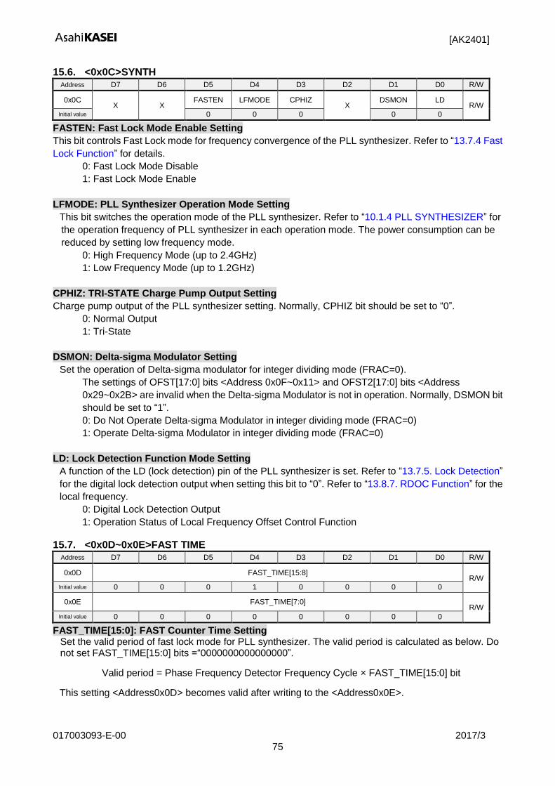
[AK2401]
017003093-E-00 2017/3 75
15.6. <0x0C>SYNTH Address D7 D6 D5 D4 D3 D2 D1 D0 R/W
0x0C X X
FASTEN LFMODE CPHIZ X
DSMON LD R/W
Initial value 0 0 0 0 0
FASTEN: Fast Lock Mode Enable Setting
This bit controls Fast Lock mode for frequency convergence of the PLL synthesizer. Refer to “13.7.4 Fast
Lock Function” for details.
0: Fast Lock Mode Disable
1: Fast Lock Mode Enable
LFMODE: PLL Synthesizer Operation Mode Setting
This bit switches the operation mode of the PLL synthesizer. Refer to “10.1.4 PLL SYNTHESIZER” for
the operation frequency of PLL synthesizer in each operation mode. The power consumption can be
reduced by setting low frequency mode.
0: High Frequency Mode (up to 2.4GHz)
1: Low Frequency Mode (up to 1.2GHz)
CPHIZ: TRI-STATE Charge Pump Output Setting
Charge pump output of the PLL synthesizer setting. Normally, CPHIZ bit should be set to “0”.
0: Normal Output
1: Tri-State
DSMON: Delta-sigma Modulator Setting
Set the operation of Delta-sigma modulator for integer dividing mode (FRAC=0).
The settings of OFST[17:0] bits <Address 0x0F~0x11> and OFST2[17:0] bits <Address
0x29~0x2B> are invalid when the Delta-sigma Modulator is not in operation. Normally, DSMON bit
should be set to “1”.
0: Do Not Operate Delta-sigma Modulator in integer dividing mode (FRAC=0)
1: Operate Delta-sigma Modulator in integer dividing mode (FRAC=0)
LD: Lock Detection Function Mode Setting
A function of the LD (lock detection) pin of the PLL synthesizer is set. Refer to “13.7.5. Lock Detection”
for the digital lock detection output when setting this bit to “0”. Refer to “13.8.7. RDOC Function” for the
local frequency.
0: Digital Lock Detection Output
1: Operation Status of Local Frequency Offset Control Function
15.7. <0x0D~0x0E>FAST TIME Address D7 D6 D5 D4 D3 D2 D1 D0 R/W
0x0D FAST_TIME[15:8] R/W
Initial value 0 0 0 1 0 0 0 0
0x0E FAST_TIME[7:0] R/W
Initial value 0 0 0 0 0 0 0 0
FAST_TIME[15:0]: FAST Counter Time Setting Set the valid period of fast lock mode for PLL synthesizer. The valid period is calculated as below. Do not set FAST_TIME[15:0] bits =“0000000000000000”.
Valid period = Phase Frequency Detector Frequency Cycle × FAST_TIME[15:0] bit
This setting <Address0x0D> becomes valid after writing to the <Address0x0E>.

[AK2401]
017003093-E-00 2017/3 76
15.8. <0x0F~0x11>FREQ OFFSET1 Address D7 D6 D5 D4 D3 D2 D1 D0 R/W
0x0F X X X X X X
OFST1[17:16] R/W
Initial value 0 0
0x10 OFST1[15:8] R/W
Initial value 0 0 0 0 0 0 0 0
0x11 OFST1[7:0] R/W
Initial value 0 0 0 0 0 0 0 0
OFST1[17:0]: Frequency Offset Setting 1
Set frequency offset for PLL synthesizer. Setting value is in 2’s complement format and MSB is the sign
bit. Refer to “13.7.3. Frequency Offset Adjustment” for details of the frequency offset function. Set all “0”
when not using the frequency offset function.
These settings <Address0x0F> and <Address0x10> will be valid after writing to the <Address0x11>.
15.9. <0x12>LOCAL Address D7 D6 D5 D4 D3 D2 D1 D0 R/W
0x12 X X X X X X
DIVSEL[1:0] R/W
Initial value 0 1
DIVSEL[1:0]: Local Divider Setting
DIVSEL Local Divider Setting
[1] [0]
0 0 Not Divide
0 1 Divide by 2 (default)
1 0 Divide by 4
1 1 Divide by 8
15.10. <0x13>TX Address D7 D6 D5 D4 D3 D2 D1 D0 R/W
0x13 X X X X
DACCNT DACLV TXOLV[1:0] R/W
Initial value 1 0 0 0
DACCNT: DAC Power Down Control for TX_PDN Reset This setting selects whether power down the DAC or not by power down control of the transmission block by the TX_PDN pin. Refer to “13.1. Power Management” for details.
0: Do not control power down of the DAC by the TX_PDN pin 1: Control power down of the DAC by the TX_PDN pin
DACLV: DAC Operation Mode Setting
DAC operation mode is selected by DACLV bit. Refer to “10.2. Transmission Characteristics” for the output level of the DAC in each operation mode. High level mode is only available when DACVDD = 4.5 ~ 5.5V.
0: Low Level Mode (DACVDD=2.7 ~ 5.5V) 1: High Level Mode (DACVDD=4.5 ~ 5.5V)

[AK2401]
017003093-E-00 2017/3 77
TXOLV[1:0]: Driver Amplifier Output Power Setting Set the output power of driver amplifier. Refer to “10.2. Transmission Characteristics” for details.
TXOLV TX Output Power
Unit [1] [0]
0 0 -6
dBm 0 1 0
1 0 3
1 1 6
15.11. <0x14>RX Address D7 D6 D5 D4 D3 D2 D1 D0 R/W
0x14 X X
TRIMREG _PH
RXLPF_ FC
IQ_SEL ANA_ PATH
MAIN_ PATH
LPMODE R/W
Initial value 0 0 0 0 1 0
TRIMREG_PH: I/Q Orthogonal Phase Calibration Setting Select either using the calibration result of the factory setting or using setting value of PH_ADJ[4:0] bits for I/Q orthogonal phase calibration. The calibration result of factory setting is loaded by setting PFUSE_RDST bit = “1” <Address0z41>. The factory calibration conditions are LOIN Input =900MHz, 0dBm, <Address0x12> DIVSEL[1:0] bit=”01”(divided by 2). Adjust PH_ADJ[4:0] bits If the local input signal condition is different. Phase unbalancing may be improved. Normally, TRIMREG_PH bit should be set to “0”.
0: Use Calibration Result of the Factory Setting
1: Use a Value Set by PH_ADJ[4:0] bits <Address0x42> RXLPF_FC: Cutoff Frequency Setting
Set a cutoff frequency of the gain variable PGA that is composed by first order low-pass filter. Refer to ”13.5.2 Analog Filter Frequency Characteristics” for frequency characteristics. Refer to “13.8.2 Digital Filter Frequency Characteristics” for recommended settings.
0: Low Cutoff Mode 1: High Cutoff Mode
IQ_SEL: Receiving Analog Baseband Signal Output I/Q Setting
The output receiving analog baseband signal from the AOUT_P and AOUT_N pins when ANA_PATH
bit= “1” is selected.
0: Ich
1: Qch
ANA_PATH: Output Function Enable for Receiving Analog Baseband Signal
Select the output of the AOUT_P and AOUT_N pins. Normally, ANA_PATH bit should be set to “0”.
0: AOUT_P, AOUT_N pins Hi-Z
1: AOUT_P, AOUT_N pins Output Receiving Analog Baseband Signal
MAIN_PATH: Output Setting of Receiving Analog Baseband Signal
Select connection of AAF output and ADC input. Normally, MAIN_PATH bit should be set to “1”.
0: AAF Output ~ ADC Input Not Connected
1: AAF Output ~ ADC Input Connected

[AK2401]
017003093-E-00 2017/3 78
LPMODE: Receiving Analog Circuit (LNA, MIXER, PGA, AAF) Operation Mode Select an operation mode of receiving analog circuit (LNA, MIXER, PGA, AAF). Refer to “10.1.1 LNA” and “10.1.2 MIXER+PGA+AAF+ADC” for receiving performance.
0: Normal Power Mode
1: Low Power Mode
15.12. <0x15~0x16>PGA GAIN Address D7 D6 D5 D4 D3 D2 D1 D0 R/W
0x15 X X
PGAGAIN_I[5:0] R/W
Initial value 0 0 0 0 0 0
0x16 X X
PGAGAIN_Q[5:0] R/W
Initial value 0 0 0 0 0 0
PGAGAIN_I[5:0]: Ich PGA Gain Setting PGAGAIN_Q[5:0]: Qch PGA Gain Setting Set Ich/Qch PGA gain independently. AGCOFF bit= “1” <Address0x1F>
AGC function is OFF and the PGA gain settings are valid. AGCOFF bit= “0” <Address0x1F>
AGC starts operation with the default value set by PGAGAIN_I[5:0] bits. Normally, PGAGAIN_I bit and PGAGAIN_Q bit should be set to “000000”.
PGAGAIN_I , PGAGAIN_Q Gain Unit
[5] [4] [3] [2] [1] [0]
0 0 0 0 0 0 28 (default)
dB
0 0 0 0 0 1 27
0 0 0 0 1 0 26
0 0 0 0 1 1 25
・・・ ・・・
0 1 1 0 1 1 1
0 1 1 1 0 0 0
0 1 1 1 0 1 -1
・・・ ・・・
1 0 1 1 1 1 -19
1 1 0 0 0 0 -20
1 1 0 0 0 1
Do Not Use
1 1 0 0 1 0
1 1 0 0 1 1
1 1 0 1 0 0
1 1 0 1 0 1
1 1 0 1 1 0
1 1 0 1 1 1
1 1 1 X X X
(X: Do not care)

[AK2401]
017003093-E-00 2017/3 79
15.13. <0x17~0x18>CAL START Address D7 D6 D5 D4 D3 D2 D1 D0 R/W
0x17 - -
CAL LNAPD
OFS2REG OFSCAL4 OFSCAL3 OFSCAL2 OFSCAL1 R/W
Initial value 0 0 0 0 0 0
0x18 - - - -
CHOFS_AVE[1:0] AGCOFS_AVE[1:0] R/W
Initial value 0 0 0 0
Refer to “13.8.6. DC Offset Calibration” for detailed operation of DC offset calibration. CALLNAPD: LNA Power Down Setting for DC Offset Calibration of Analog Block (MIXER)
This bit set ON/OFF of LNA power down function for initial DC offset calibration of the analog block. LNA is powered down during calibration by setting OFSCAL1 bit = “1” and powered up automatically after the calibration is finished. This setting is only valid when PD_LNA_N bit = “1” <Address 0x2E>. Normally, CALLNAPD bit should be set to “1”.
0: Do not power down the LNA during the DC offset calibration of the analog block (MIXER) 1: Power down the LNA during the DC offset calibration of the analog block (MIXER)
OFS2REG: External Input Setting for DC Offset Compensation Value
This bit selects DC offset compensation value source for the channel filter block. When it is “1”, setting value of I ch or Q ch <Address 0x19 ~ 0x1E> is used for offset compensation instead of using calibration result by OFSCAL2 bit. Normally, OFS3REF bit should be set to “0”.
0: Use Calibration Result for DC Offset Compensation for the Channel Filter 1: Use Register Settings for DC Offset Compensation for the Channel Filter
OFSCAL4: Start Trigger of DC Offset Calibration for Digital (AGC) Block DC offset calibration for digital (AGC) block starts by writing “1” to this bit. This bit returns to “0” automatically after the calibration is finished.
OFSCAL3: Start Trigger of DC Offset Calibration for Digital (Channel Filter) Block DC offset calibration for digital (Channel Filter) block starts by writing “1” to this bit. This bit returns to “0” automatically after the calibration is finished.
OFSCAL2: Start Trigger of DC Offset Calibration for Digital (Channel Filter + AGC) Block DC offset calibration for digital (Channel Filter + AGC) block starts by writing “1” to this bit. This bit returns to “0” automatically after the calibration is finished.
OFSCAL1: Start Trigger of DC Offset Calibration for Analog Block (MIXER) DC offset calibration for analog block (MIXER) starts by writing “1” to this bit. This bit returns to “0” automatically after the calibration is finished.
CHOFS_AVE[1:0]: Averaging Time of Calibration for Digital (Channel Filter) Block Set the time of sampling data averaging process during the DC offset calibration of channel filter block.
AGCOFS_AVE[1:0]: Averaging Time of Calibration for Digital (AGC) Block Set the time of sampling data averaging process during the DC offset calibration of AGC block.

[AK2401]
017003093-E-00 2017/3 80
15.14. <0x19~0x1E>CH_DC OFST Address D7 D6 D5 D4 D3 D2 D1 D0 R/W
0x19 OFST_I[23:16] R/W
Initial value 0 0 0 0 0 0 0 0
0x1A OFST_I[15:8] R/W
Initial value 0 0 0 0 0 0 0 0
0x1B OFST_I[7:0] R/W
Initial value 0 0 0 0 0 0 0 0
0x1C OFST_Q[23:16] R/W
Initial value 0 0 0 0 0 0 0 0
0x1D OFST_Q[15:8] R/W
Initial value 0 0 0 0 0 0 0 0
0x1E OFST_Q[7:0] R/W
Initial value 0 0 0 0 0 0 0 0
OFST_I[23:0]: Ich DC Offset Compensation Value
OFST_Q[23:0]: Qch DC Offset Compensation Value
Set these bit to define DC offset compensation value arbitrarily for the channel filter block. This setting will
be valid instead of initial calibration value by setting OFS2REG bit = “1” <Address 0x17>.
The setting of <Address0x19> and <Address0x1A> will be valid when writing to the <Address0x1B>.
The setting of <Address0x1C> and <Address0x1D> will be valid when writing to the <Address0x1E>.
15.15. <0x1F~0x21, 0x47~048>AGC Address D7 D6 D5 D4 D3 D2 D1 D0 R/W
0x1F AGCTIM[2:0] AGCHYS[1:0] AGC_
KEEPSEL AGC_
KEEPR AGCOFF
R/W
Initial value 0 1 1 0 0 0 0 1
0x20 LNA_
AGC_OFF LNA_
LGMODE AGCMAX[2:0] AGCTGT[2:0]
R/W Initial value 1 0 1 1 1 0 1 0
0x21 X X
FB_RDOC AGCKP_MODE[1:0] AGCTRW[2:0] R/W
Initial value 0 0 0 0 1 1
0x47 X X
LNA_TGT_H[5:0] R/W
Initial value 1 0 0 0 1 0
0x48 X X
LNA_TGT_L[5:0] R/W
Initial value 1 0 1 1 1 0
Note that <Address0x47> and <Address0x48> are written in this document in a reverse order. Refer to “13.8.8 AGC” and “13.8.9 AGC_KEEP” for AGC operation related to these settings above

[AK2401]
017003093-E-00 2017/3 81
AGCTIM[2:0]: Calculation/Detection Time Setting of Signal Power Set signal power calculation/detection time of AGC. The power calculation/detection time is calculated by the equation shown below. Power calculation/detection times in the case of using 18.432MHz and 19.2MHz reference clocks are shown in the table below.
Power Calculation/Detection Time = Reference Clock Cycle × 2048 ×2
N
*N: AGCTIM bits Setting Value
AGCTIM Power Calculation/Detection Time Unit
[2] [1] [0] 18.432MHz 19.2MHz
0 0 0 0.11 0.11
msec
0 0 1 0.22 0.21
0 1 0 0.44 0.43
0 1 1 0.89 (default) 0.85 (default)
1 0 0 1.79 1.71
1 0 1 3.56 3.41
1 1 0 7.11 6.83
1 1 1 14.22 13.65
AGCHYS[1:0]: Hysteresis Width of Signal Power Convergence Level AGC (Automatic Gain Control) stops gain controlling when the current receiving level is within the range of this setting (convergence detection level) against the AGC convergence target level set by AGCTGT[2:0] bits <Address 0x20>.
AGCHYS Convergence Detection Level Unit
[1] [0]
0 0 < ±1 (default)
dB 0 1 < ±2
1 0 < ±4
1 1 < ±8
AGC_KEEP_SEL: Control Method Setting for the AGC_KEEP Function
This bit selects register or pin control of the AGC_KEEP function.
0: Control by AGC_KEEPR bit
1: Control by the AGC_KEEP pin
AGC_KEEPR: ON/OFF Setting of the AGC KEEP Function
Set ON/OFF of the AGC KEEP function. This setting will only be valid when setting AGC_KEEP_SEL bit
= “0” <Address 0x1F>
0: AGC KEEP Function OFF
1: AGC KEEP Function ON
AGCKP_MODE bit <Address 0x21> controls operation of the AGC KEEP function.
AGCOFF: ON/OFF Setting of AGC (Automatic Gain Control) Function
Set ON/OFF of the AGC function. AGC is performed in PGA and LNA blocks. LNA gain control can be
applied to PGA by setting LNA_AGCOFF bit = “0” <Address0x20> when AGCOFF bit= “0”. Normally
AGCOFF bit should be set to “0”.
0: AGC Function ON
1: AGC Function OFF

[AK2401]
017003093-E-00 2017/3 82
LNA_AGCOFF: LNA Gain Control Switching
LNA gain control can be applied to PGA gain setting. Normally, LNA_AGCOFF bit should be set to “0”
0: PGA gain is controlled by LNA gain control
1: PGA gain is not controlled by LNA gain control.
LNA_LGMODE: LNA Low Gain Mode
LNA low gain mode is available by setting LNA_LGMODE bit=“1”. This setting is only valid when
LNA_AGCOFF bit= “1” <Address0x20>. LNA gain mode can be changed manually.
0: Normal Gain Mode
1: Low Gain Mode
AGCMAX[2:0]: Maximum Tolerate Gain Change Amount for Single AGC Operation
Set the maximum tolerate of gain change amount for single AGC operation.
AGCMAX Max Tolerate Gain Change Unit
[2] [1] [0]
0 0 0 Do Not Use This Setting
dB
0 0 1 1
0 1 0 2
0 1 1 4
1 0 0 8
1 0 1 16
1 1 0 32
1 1 1 48 (default)
AGCTGT[2:0]: Signal Power Convergence Target Level
Set the target level of AGC convergence.
AGCTGT Convergence Level Unit
[2] [1] [0]
0 1 1 6
dBm
0 1 0 4 (default)
0 0 1 2
0 0 0 0
1 1 1 -2
1 1 0 -4
1 0 1 -6
1 0 0 -8
FB_RDOC: Reflect RDOC Compensation Value to Digital (AGC) Block
DC offset value detected by RDOC will be reflected to Digital (AGC) block when FB_RDOC bit= “1”.
0: RDOC Compensation Value is not reflected to Digital (AGC) block.
1: RDOC Compensation Value is reflected to Digital (AGC) block.

[AK2401]
017003093-E-00 2017/3 83
LNA_TGT_H[5:0]: LNA Gain Mode Switching Threshold (High)
LNA_TGT_L[5:0]: LNA Gain Mode Switching Threshold (Low)
Set LNA gain mode switching threshold of when LNA_AGCOFF bit= “0”<Address0x20>. Threshold
setting corresponds to each PGA gain settings. The setting values must be LNA_TGT_H >
LNA_TGT_L. In case of setting values such as LNA_TGT_H ≤ LNA_TGT_L, the same value set to
LNA_TGT_L will be set to LNA_TGT_H. The difference between LNA_TGT_H and LNA_TGT_L should
be bigger than LNA gain that is decreased by changing to Low gain mode. Here, LNA_TGT_H and
LNA_TGT_L mean PGA gain threshold (dB) not register values.
LNA_TGT_H, LNA_THT_L PGA Gain Threshold
Unit [5] [4] [3] [2] [1] [0]
0 0 0 0 0 0 28
dB
0 0 0 0 0 1 27
0 0 0 0 1 0 26
0 0 0 0 1 1 25
・・・ ・・・
0 1 1 0 1 1 1
0 1 1 1 0 0 0
0 1 1 1 0 1 -1
0 1 1 1 1 0 -2
0 1 1 1 1 1 -3
1 0 0 0 0 0 -4
1 0 0 0 0 1 -5
1 0 0 0 1 0 -6 (default, LNA_TGT_H)
・・・ ・・・
-18 (default, LNA_TGT_L)
1 0 1 1 1 1 -19
1 1 0 0 0 0 -20
1 1 0 0 0 1
Do not use
1 1 0 0 1 0
1 1 0 0 1 1
1 1 0 1 0 0
1 1 0 1 0 1
1 1 0 1 1 0
1 1 0 1 1 1
1 1 1 X X X
(X: Do not care) AGCKP_MODE[1:0]: AGC KEEP Function Operation
Select the operation mode of AGC KEEP function.
Refer to “13.8.9 AGC_KEEP” for details.

[AK2401]
017003093-E-00 2017/3 84
AGCTRW[2:0]: AGC Power Detection Wait Time
Set the wait time of power detection starts after PGA gain is changed in AGC operation.
AGCTRW Wait Time Unit
[2] [1] [0]
0 0 0 0.125
msec
0 0 1 0.25
0 1 0 0.5
0 1 1 1 (default)
1 0 0 2
1 0 1 4
1 1 0 8
1 1 1 16
15.16. <0x22>CH FILTER Address D7 D6 D5 D4 D3 D2 D1 D0 R/W
0x22 DFIL_SR[1:0] DFIL_ PROG
DFIL_CLK DFIL_SEL[3:0] R/W
Initial value 0 0 0 0 0 0 0 0
Refer to “13.8.2 Digital Filter Frequency Characteristics”, “13.8.3 Programmable FIR” and “13.8.11 Output Sampling Rate” for details of these settings. DFIL_SR[1:0]: Output Sampling Rate
Select the sampling rate of digital filter outputs. DFIL_PROG: Programmable FIR Filter Setting
Select normal channel filter or a programmable FIR Filter.
0: Use Normal Channel Filter set by DFIL_SEL[3:0] bits <Address 0x22>
1: Use a programmable FIR Filter set by <Address 0x2D> as Channel Filter DFIL_CLK: Reference Clock Setting
Set reference clock that is input to the TCXOIN pin
0: 19.2MHz
1: 18.432MHz DFIL_SEL[3:0]: Channel Filter Setting
Set Normal Channel Filter
15.17. <0x23>PROG FILTER Address D7 D6 D5 D4 D3 D2 D1 D0 R/W
0x23 X X
PFIL_SAT[2:0] PFIL_SIFT[2:0] R/W
Initial value 0 0 0 0 0 0
PFIL_SAT[2:0]: Saturation Process Setting for Programmable FIR Filter Output
Set the number of bit for saturation process that is applied to the programmable FIR filter outputs.
PFIL_SIFT[2:0]: Bit Shift Setting for Programmable FIR Filter Output Set the number of bit and sift direction (right or left) of bit shifting process that is applied to the programmable FIR filter outputs.

[AK2401]
017003093-E-00 2017/3 85
15.18. <0x24~0x25>HPF Address D7 D6 D5 D4 D3 D2 D1 D0 R/W
0x24 X X
HPF_ FAST
HPF_FC[3:0] HPFSEL R/W
Initial value 0 0 0 0 0 0
0x25 X
FAST_GAIN[1:0] FAST_FC[1:0] HPF_FTIM[2:0] R/W
Initial value 0 0 0 0 0 0 0
Refer to “13.8.4. High-Pass Filter” and “13.8.5. Fast Track Mode” for details of these settings.
HPF_FAST: Fast Track Mode Setting Set ON/OFF of the Fast Track Mode. In this mode, the cutoff frequency of HPF is switched to a higher frequency temporary to convergent DC offset change that occurs when changing PGA gain in AGC operation or when power down the receiving block.
0: Fast Track Mode OFF
1: Fast Track Mode ON
HPF_FC[3:0]: Digital High-Pass Filter Cutoff Frequency Set the HPF cutoff frequency.
HPFSEL: High-Pass Filter ON/OFF Setting Set ON/OFF of high-pass filter.
0: HPF OFF
1: HPF ON *This bit must not be set to “1” when <Address 0x26> RDOC bit = “1” <Address 0x26>.
FAST_GAIN[1:0]: Gain Change Amount Setting for Fast Track Mode Trigger Set PGA gain change amount for the trigger of Fast Track mode when <Address 0x24> HPF_FAST bit = “1”. Fast Track mode will be enabled when PGA gain is changed more than the setting amount of this register in a one AGC operation.
FAST_FC[1:0]: Cutoff Frequency Setting in Fast Track Mode Set the higher cutoff frequency that is temporary used in Fast Track Mode.
HPF_FTIM[2:0]: Cutoff Frequency Switching Time in Fast Track Mode Set the switching time of the cutoff frequency in Fast Track mode.

[AK2401]
017003093-E-00 2017/3 86
15.19. <0x26~0x28, 0x44~0x46>RDOC Address D7 D6 D5 D4 D3 D2 D1 D0 R/W
0x26 RDOC_1 RDOC_2 KEEP_ RDOC
RDOC_3[1:0] RDOC_4[1:0] RDOC R/W
Initial value 0 1 0 1 0 0 1 0
0x27 X
RDOC_5[2:0] RDOC_6[1:0] RDOC_7[1:0] R/W
Initial value 0 1 0 0 0 0 1
0x28 X
RDOC_8[1:0] OFST_RSEL[1:0] RDOC_
FM RDOC_9[1:0]
R/W Initial value 0 0 0 0 0 0 0
0x44 R_RDOC RDOC_10[1:0] RDOC_11[1:0] RDOC_12[2:0] R/W
Initial value 0 0 0 0 0 1 0 1
0x45 RDOC_13[7:0] R/W
Initial value 0 0 0 0 0 0 0 1
0x46 RDOC_14[1:0] RDOC_15[1:0] RDOC_16[1:0] RDOC_17[1:0] R/W
Initial value 1 1 0 0 0 0 0 0
Note that <Address0x44>, <Address0x45> and <Address0x46> are written in this document in a reverse order.
Refer to “13.8.7 RDOC” for details. Following registers are RDOC operation registers. These registers excluding RDOC_7[1:0], RDOC_8[1:0] bits must be in the default setting. RDOC_7[1:0], RDOC_8[1:0] bits must be set to “11”
Register Address Initial Value Recommended
RDOC_1 0x26 D7 “0” “0”
RDOC_2 0x26 D6 “1” “1”
RDOC_3 0x26 D4-D3 “10” “10”
RDOC_4 0x26 D2-D1 “01” “01”
RDOC_5 0x27 D6-D4 “010” “010”
RDOC_6 0x27 D3-D2 “00” “00”
RDOC_7 0x27 D1-D0 “01” “11”
RDOC_8 0x28 D6-D5 “00” “11”
RDOC_9 0x28 D1-D0 “00” “00”
RDOC_10 0x44 D6-D5 “00” “00”
RDOC_11 0x44 D4-D3 “00” “00”
RDOC_12 0x44 D2-D0 “101” “101”
RDOC_13 0x45 D7-D0 “00000001” “00000001”
RDOC_14 0x46 D7-D6 “11” “11”
RDOC_15 0x46 D5-D4 “00” “00”
RDOC_16 0x46 D3-D2 “00” “00”
RDOC_17 0x46 D1-D0 “00” “00”
KEEP_RDOC: Interlock Setting with AGC KEEP Function The RDOC function can be interlocked with the AGC KEEP function by setting this bit. If this bit is “1”, the RDOC cancellation function will be OFF when setting the AGC_KEEP pin = “H” or AGC_KEEPR = “1”. In this time, the calculated DC offset value is kept. The RDOC function will be enabled again when setting the AGC_KEEP pin = “L” or AGC_KEEPR bit = “0”.
0: Do Not Interlock RDOC Function with AGC KEEP Function
1: Interlock RDOC Function with AGC KEEP Function

[AK2401]
017003093-E-00 2017/3 87
RDOC: RDOC ON/OFF Setting Set ON/OFF of RDOC.
0: RDOC OFF
1: RDOC ON
OFST_RSEL[1:0]: DC Offset Readback Data Select Readback data of DC offset cancellation in 15.25 <0x31~0x36>READ OFST can be selected.
OFST_RSEL Readback Data in 15.25 <0x31~0x36>READ OFST
[1] [0]
0 0 [1] Digital Block (Channel Filter) DC Offset Calibration Value
0 1 [2] RDOC Value
1 0 Total Value of [1] + [2]
1 1 Digital Block (AGC) DC Offset Calibration Value
RDOC_FM: RDOC setting for FM radio Set RDOC_FM bit = “1” when receiving unmodulated (CW) signals such as FM radio with RDOC function. Refer to 13.8.7 RDOC Function for details.
R_RDOC: Operation Status Readback for RDOC Function Current operation status can be read by R_RDOC bit. It is not normally used.

[AK2401]
017003093-E-00 2017/3 88
15.20. <0x29~0x2B>FREQ OFFSET2 Address D7 D6 D5 D4 D3 D2 D1 D0 R/W
0x29 X X X X X X
OFST2[17:16] R/W
Initial value 0 0
0x2A OFST2[15:8] R/W
Initial value 0 0 0 0 0 0 0 0
0x2B OFST2[7:0] R/W
Initial value 0 0 0 0 0 0 0 0
OFST2[17:0]: Frequency Offset Setting 2
Set frequency offset for PLL synthesizer. Setting value is in 2’s complement format and MSB is the sign
bit. Refer to “13.7.3. Frequency Offset Adjustment” for details of the frequency offset function. It is
recommended to set the offset frequency (OFST2 bits) to become 150Hz after divided by the local
divider. Set all “0” when not using the RDOC function. This setting is only valid when RDOC_FM bit = “1”
<Address0x28>. Refer to “13.8.7. RDOC Function” for details.
The setting of <Address0x29> and <Address0x2A> will be valid when writing to the <Address0x2B>.
15.21. <0x2C>RSSI Address D7 D6 D5 D4 D3 D2 D1 D0 R/W
0x2C X X X
RSSI_LOW[1:0] RSSIAVE[2:0] R/W
Initial value 0 0 0 0 0
Refer to “13.8.10. RSSI” for setting details.
RSSILOW[1:0]: RSSI Compensation
Set a compensation value of RSSI code. The RSSI function subtracts the RSSI compensation value
from a detected signal level and outputs as RSSI code. The smaller the compensation value is the
smaller signal level can be detected.
RSSI_LOW Compensation Value [dB] [1] [0]
0 0 18 (default)
0 1 12
1 0 6
1 1 0

[AK2401]
017003093-E-00 2017/3 89
RSSIAVE[2:0]: RSSI Averaging Setting
The signal from RSSI circuit is averaged by output sampling rate. Set the number of averaging
operation by RSSIAVE bits. The setting of the output sampling rate is DFIL_SR[1:0] bits = “00”
<Address0x22>.
RSSIAVE Averaging [Times]
[2] [1] [0]
0 0 0 4 (default)
0 0 1 8
0 1 0 16
0 1 1 32
1 0 0 64
1 0 1
128 1 1 0
1 1 1
15.22. <0x2D>FIR COEF Address D7 D6 D5 D4 D3 D2 D1 D0 R/W
0x2D COEF_NUM[6:0] COEF_ST R/W
Initial value 0 0 0 0 0 0 0 0
Refer to “13.8.3. Programmable FIR” for setting details.
COEF_NUM[6:0]: TAP Number Setting for Programmable FIR Filter
Set the TAP number of programmable FIR filter. This setting must be in the range shown below. If the
setting of COEF_NUM bits is more than 75, it will be recognized as 75 as the limit of the setting.
<Address0x22> DFIL_SEL[3:0] bits = 0~3(dec): 1 ≤ COEF_NUM ≤ 64
<Address0x22> DFIL_SEL[3:0] bits = 4~15(dec): 1 ≤ COEF_NUM ≤ 75
The AK2401 cannot be in FIR filter coefficient write mode even if COEF_ST bit is set to “1” when
COEF_NUM[6:0] bits are set to “0000000”. Therefore, it is recommended to set COEF_NUM[6:0] bits
“0000000” after writing coefficient to prevent unintended change of the setting.
COEF_ST: Start Trigger of Coefficient Write Mode
When setting this bit to “1”, the serial interface for register writing enters FIR filter coefficient write mode.
Write coefficient continuously for the number of times of the TAP number set by COEF_NUM[6:0] bits.
COEF_ST bit returns to “0” automatically after finish writing the coefficient and normal register write
becomes available.

[AK2401]
017003093-E-00 2017/3 90
15.23. <0x2E>PD Address D7 D6 D5 D4 D3 D2 D1 D0 R/W
0x2E PD_
CLKBUF_N PD_
LNA_N PD_
RXR_N PD_
TXR_N PD_
SYNTH_N PD_
ADC_N PD_
DAC_N PD_
REF_N R/W Initial value 0 0 0 0 0 0 0 0
Control each block power down. Refer to “13.1. Power Management” for details.
15.24. <0x2F~0x30>READ PGA Address D7 D6 D5 D4 D3 D2 D1 D0 R/W
0x2F X
R_LNA_ LGMODE
RPGA_I[5:0] R
Initial value 0 0 0 0 0 0 0
0x30 X X
RPGA_Q[5:0] R
Initial value 0 0 0 0 0 0
R_LNA_LGMODE: LNA Gain Mode Readback (Readback Only)
Gain mode of the low noise amplifier is readback by writing the register addresses of this register. “0”
indicates Normal Gain Mode and “1” indicates Low Gain Mode. AGC calculation result is readback
when LNA_AGCOFF bit = “0”. The setting value of LNA_LGMODE bit will be readback when
LNA_AGCOFF bit = “1”.
RPGA_I[5:0]: Ich PGA Gain Readback (Readback Only)
RPGA_Q[5:0]: Qch PGA Gain Readback (Readback Only)
Setting gain of programmable gain amplifier is readback by writing the register addresses of these
settings above. AGC calculation result is readback when AGCOFF bit = “0” <Address 0x1E>. The
setting values of PGAGAIN_I[5:0] bits <Address 0x15> and PGAGAIN_Q[5:0] bits <Address 0x16> will
be readback when AGCOFF bit = “1”.
15.25. <0x31~0x36>READ OFST Address D7 D6 D5 D4 D3 D2 D1 D0 R/W
0x31 R_OFST_I[23:16] R
Initial value 0 0 0 0 0 0 0 0
0x32 R_OFST_I[15:8] R
Initial value 0 0 0 0 0 0 0 0
0x33 R_OFST_I[7:0] R
Initial value 0 0 0 0 0 0 0 0
0x34 R_OFST_Q[23:16] R
Initial value 0 0 0 0 0 0 0 0
0x35 R_OFST_Q[15:8] R
Initial value 0 0 0 0 0 0 0 0
0x36 R_OFST_Q[7:0] R
Initial value 0 0 0 0 0 0 0 0
R_OFST_I[23:0]: Ich DC Offset Calibration Result (Readback Only)
R_OFST_Q[23:0]: Qch DC Offset Calibration Result (Readback Only)
DC offset value set by OFST_RSEL[1:0] bits <Address 0x28> are readback.

[AK2401]
017003093-E-00 2017/3 91
15.26. <0x37~0x39>READ COEF Address D7 D6 D5 D4 D3 D2 D1 D0 R/W
0x37 X
TAPNUM[6:0] R/W
Initial value 0 0 0 0 0 0 0
0x38 R_COEF[15:8] R
Initial value 0 0 0 0 0 0 0 0
0x39 R_COEF[7:0] R
Initial value 0 0 0 0 0 0 0 0
Refer to “13.8.3. Programmable FIR” for details of these setting.
TAPNUM[6:0]: TAP Specifying for Programmable FIR Filter Coefficient Readback
Specify the TAP when readback the coefficient set to the programmable FIR filter <Address 0x38,
0x39>.
R_COEF[15:0]: Programmable FIR Filter Coefficient Readback (Readback Only)
Readback the coefficient set to the programmable FIR filter.
The coefficient that is specified by <Address 0x37> TAPNUM[6:0] bits is readback.
15.27. <0x3A>READ RSSI Address D7 D6 D5 D4 D3 D2 D1 D0 R/W
0x3A RSSI[7:0] R
Initial value 0 0 0 0 0 0 0 0
RSSI[7:0]: RSSI Result (Readback Only)
Readback RSSI result. Refer to “13.8.10. RSSI” for details.
15.28. <0x3B~0x3E>ANA DC OFST Address D7 D6 D5 D4 D3 D2 D1 D0 R/W
0x3B X X
OFST1H_I[5:0] R/W
Initial value 0 0 0 0 0 0
0x3C X X
OFST1H_Q[5:0] R/W
Initial value 0 0 0 0 0 0
0x3D X X
OFST1L_I[5:0] R/W
Initial value 0 0 0 0 0 0
0x3E X X
OFST1L_Q[5:0] R/W
Initial value 0 0 0 0 0 0
OFST1H_I[5:0]: DC Offset Calibration Result of Analog Block (Ich Normal Power Mode)
OFST1H_Q[5:0]: DC Offset Calibration Result of Analog Block (Qch Normal Power Mode)
OFST1L_I[5:0]: DC Offset Calibration Result of Analog Block (Ich Low Power Mode)
OFST1L_Q[5:0]: DC Offset Calibration Result of Analog Block (Qch Low Power Mode)

[AK2401]
017003093-E-00 2017/3 92
DC offset calibration result of the analog block that is executed by OFSCAL1 bit = “1” <Address 0x17>
can be readout. The calibration result will be stored at <Address 0x3B and 0x3C> if the calibration mode
is set to normal mode LPMODE bit = “0” <Address 0x14>. The calibration result will be stored at
<Address 0x3D and 0x3E> if the calibration mode is set to low power mode LPMODE bit = “1” <Address
0x14>.
By writing to these registers, a register setting value can be used instead of the calibration result. Note
that the calibration result will be over written in this case.
15.29. <0x3F~0x40>LDCNT Address D7 D6 D5 D4 D3 D2 D1 D0 R/W
0x3F LD_LOCKCNT[7:0] R/W
Initial value 0 0 1 1 1 1 1 1
0x40 LD_UNLOCKCNT[7:0] R/W
Initial value 0 0 1 1 1 1 1 1
LD_LOCKCNT[7:0]: Lock Detection Accuracy Setting
LD_UNLOCKCNT[7:0]: Unlock Detection Accuracy Setting
Set the number of detection time for digital lock/unlock detection mode. Refer to “13.7.5. Lock
Detection” for details.
*Do not set LD_LOCKCNT bit= “00000000” or LD_UNLOCKCNT bit= “00000000”.
15.30. <0x41~0x43>PHASE CAL Address D7 D6 D5 D4 D3 D2 D1 D0 R/W
0x41 X X X X X X X
PFUSE_ RDST R/W
Initial value 0
0x42 X X
PH_ADJ[5:0] R/W
Initial value 1 0 0 0 0 0
0x43 X X
R_PH_ADJ[5:0] R
Initial value 0 0 0 0 0 0
PFUSE_RDST: Loading Trigger of I/Q Orthogonal Phase Calibration Value
When this bit is set to “1”, the I/Q orthogonal phase calibration value is loaded. It must be executed once
after hardware reset by the RSTN pin. This bit returns to “0” automatically, after finishing the load. Refer
to “13.6.3. Phase Calibration” for details.
* The loading value will not be reset by the software reset controlled by SRST[7:0] bits <Address 0x5F>.

[AK2401]
017003093-E-00 2017/3 93
PH_ADJ[5:0]: I/Q Orthogonal Phase Calibration Setting
Set I/Q orthogonal phase calibration value directly. This setting is only valid when TRIMREG_PH bit =
“1” <Address0x14>.
PH_ADJ Ich Qch Unit
[5] [4] [3] [2] [1] [0]
0 0 0 0 0 X -3.875 0
deg
0 0 0 0 1 0 -3.75 0
0 0 0 0 1 1 -3.625 0
・・・ ・・・
0 1 1 1 1 0 -0.25 0
0 1 1 1 1 1 -0.125 0
1 0 0 0 0 0 0 0
1 0 0 0 0 1 0 -0.125
1 0 0 0 1 0 0 -0.25
・・・ ・・・
1 1 1 1 0 1 0 -3.625
1 1 1 1 1 0 0 -3.75
1 1 1 1 1 1 0 -3.875
(X: Do not care)
R_PH_ADJ[5:0]: I/Q Orthogonal Phase Adjustment Calibration Value Readback (Readack Only)
Readback I/Q orthogonal phase calibration value set by TRIMREG_PH bits <Address0x14>.
* Refer to “15.19. <0x26~0x28, 0x44~0x46>RDOC” for register description of
<Address0x44>,<Address0x45> and <Address0x46>.
* Refer to “15.15. <0x1F~0x21, 0x47~048>AGC” for register description of <Address0x47> and
<Address0x48>.
15.31. <0x49>PRE TESTEN Address D7 D6 D5 D4 D3 D2 D1 D0 R/W
0x49 PRE_
TSTWE
X X X X X X X R/W Initial value 0
PRE_TSTWE: Pre Test Register Enable
Register writing to the <Address0x4A> and <Address0x4B> become valid when setting PRE_TSTWE bit = “1”.

[AK2401]
017003093-E-00 2017/3 94
15.32. <0x4A>CH FILTER2 Address D7 D6 D5 D4 D3 D2 D1 D0 R/W
0x4A X X X X X
TEST_1 DFIL_ACC DFIL_ CLKG R/W
Initial value 1 0 0
TEST_1 bit is a test bit. Write “1” to this bit.
DFIL_ACC : Digital Filter Accumulator Calculation Method Setting Set the calculation method of the digital filter. Spurious of the operation frequency of the digital filter (such as TCXO/4) will be changed. Normally, DFIL_ACC bit must be set to “0”.
0: PRBS (default)
1: Homogenized
DFIL_CLKG : Digital Filter Clock Gating Setting Set ON/OFF of the clock gating of the digital filter. Spurious of the operation frequency of the digital filter (such as TCXO/4) will be reduced. Normally, DFIL_CLKG bit must be set to “1”.
0: Clock Gating OFF (default)
1: Clock Gating ON (recommended)
15.33. <0x4B>STATUS Address D7 D6 D5 D4 D3 D2 D1 D0 R/W
0x4B TEST_2 TEST_3 TEST_4 TEST_5 LNALG_
STS AGC_STS RSSI_STS
HPFFT_ STS R/W
Initial value 0 0 0 0 0 0 0 0
When writing “0” to this register, each status bit at ADC output serial interface is masked and outputs “0”. When writing “1” to this register, each status bit will output status of corresponding block.
Refer to “13.8.12. ADC P/S IF” for details.
15.34. <0x5F>SOFT RESET Address D7 D6 D5 D4 D3 D2 D1 D0 R/W
0x5F SRST [7:0] R/W
Initial value 0 0 0 0 0 0 0 0
SRST[7:0]: Software Reset
Software reset is executed by writing to SRST[7:0] bits = “10101010”. This register will return to
“00000000” automatically when the software reset is completed. Refer to “9.2. System Reset” for
details.

[AK2401]
017003093-E-00 2017/3 95
16. Recommended External Circuits
16.1. Recommended External Circuits
16.2. List of Parts Table 11. Parts List for External Circuit Connection
Ref. Value Description Ref. Value Description
LG 30nH
LNAIN=450MHz Normal Power Mode
T1 4:1 RFOUT=450MHz
JTX-4-10T
LS 3.3nH RO1 100Ω
C2 3.6pF RO2 100Ω
C1 100pF RS2 -
LOOP FILTER
LD - RS2’ -
D1 - RS3 -
LG 47nH
LNAIN=450MHz Low Power Mode
CS1 -
LS 3.3nH CS2 -
C2 1.3pF CS3 -
C1 100pF CS4 1000pF
LD - C7 100pF
D1 - CB13 10μF
RL 200Ω
LNAOUT=450MHz
CP13 100pF
L1 27nH CB14 0.47μF
C4 3.9pF CB15 2.2μF
L2 220nH
DEMIN=450MHz
RB1 47kΩ ±1% recommended
L3 22nH RB2 27kΩ ±1% recommended
C5 20pF
*Coil inductors are used. *Matching circuit examples at frequencies other than 450 MHz are prepared as application notes. Contact us separately. *DAN217UM is used for the diode LD.
28. LNAINC1
LS
D1 C2
LG
LD29. LNACONT
25. L
NA
OU
T
23. D
EM
IN
VDD
C4 C5
L3
L2
RL L1
OPTIONAL BPF
20. R
FO
UT
N
19. R
FO
UT
P
RO2 RO1
31. BIAS1
33. AOUT_P
34. AOUT_N
38. VCOM_ADCB15
RB1
39.
RS
TN
40.
RX
_P
DN
41.
TX
_P
DN
42.
AG
C_
KE
EP
43.
CS
N
44.
SD
AT
AI
45.
SC
LK
46.
SD
AT
AO
47.
LD
49.
AD
_S
CLK
50.
AD
_S
DO
51.
AD
_F
S
52.
DA
_F
S
MCU/DSP
18. L
OIN
14. C
P
15. S
WIN
16. C
PZ
CS1RS2'
CS2
RS2
RS3 CS3
VCO
OPTIONALLPF
CS4
1.
DA
_S
CLK
3.
DA
_S
DI
8. VREF1
CB14
C7
9. TCXOIN
10. VREF2 CB13
CP13
6. SMFOUT RB2
5. BIAS2
TAB
35.
TE
ST
2
4.
TE
ST
1
T1

[AK2401]
017003093-E-00 2017/3 96
16.3. Power Supply/Ground Pin Connect capacitors between VDD and VSS pins to eliminate ripple and noise included in power supply. For a maximum effect, the capacitors should be located at the shortest distance between these pins.
LSI
C4
LNAVDD
C1
C4=10F
C1=100pF
30
C2
C2=0.01F
DEMVDD
C1
24
LOVDD
C1
21
CPVDD
C1
13
C4
SYNVDD
C1
12
DACVDD
C1
7
RXVDD
C1
32
ADVDD
C1
37
C3
DVDD
C1
48
LODVDD
17
C3=1F

[AK2401]
017003093-E-00 2017/3 97
16.4. PCB Design Below are board design guidelines confirmed by the conditions of our evaluation board and do not specify layout pattern of customer's board or guarantee the characteristics. - Connect the exposed pad in the center of the back to the low impedance analog ground. If the
exposed pad is not mounted, the operation may become unstable. - The ADC is a 24-bit delta-sigma A/D converter. ADC operation clock is generated by dividing a
reference clock that is input to the TCXOIN pin by four. For this reason, since (TCXO/4) MHz and its harmonic components leak to the input part of the LNA, selecting that frequency as the RF frequency causes suppression of receiver sensitivity. Therefore, if customer’s RF frequency is equal to multiplied by (TCXO/4) MHz, evaluate its performance with customer’s board. On our evaluation board we confirm that the suppression of receiver sensitivity will be relaxed by paying attention to the guidelines described below.
- Each VSS is not separated and connected to the same analog ground. - Spurious characteristics are improved by short-circuiting the exposed pad and each VSS pin with the
TOP layer of the PCB. - Power supply pins need to be careful not to go around LNA because ADVDD/DVDD is the main
spurious source. In addition to connecting a 100pF decoupling capacitor to each power supply pin, 10nF is added to LNAVDD and 1uF is added to ADVDD.
- Each power supply pin is wired in low impedance from LDO etc. without connecting ferrite beads in series. Improvement of spurious characteristics is confirmed by connecting 1Ω in series only for LNAVDD.
- Spurious characteristics degrade due to high frequency noise of AD_SCLK, AD_SDO, AD_FS pins. Put 100Ω damping resistance in series. Fill the digital signal line in the inner layer.
- Connect decoupling capacitors, especially small capacitance ceramic capacitors as closely as possible to AK2401.
- Use a balun connected to RFOUT_P, RFOUT_N pins depending on the frequency band. Because it is an open collector pin, when using a balun without a center tap, it is necessary to supply the power supply voltage separately through an inductor.
- For VREF1, VREF2 pins capacitor connected to ground, stabilize the internal circuit, connect the specified value.
- All digital input pins must not be allowed to float.

[AK2401]
017003093-E-00 2017/3 98
16.5. PCB Layout

[AK2401]
017003093-E-00 2017/3 99
17. LSI Interface Circuit
Pin# Name I/O R0[] Function
1 DA_SCLK I 300
Digital Input Pin
R0
3 DA_SDI I 300
39 RST_N I 300
40 RX_PDN I 300
41 TX_PDN I 300
42 AGC_KEEP I 300
43 CSN I 300
44 SDATAI I 300
45 SCLK I 300
52 DA_FS I 300
4 TEST1 I 300 Digital Input Pin Pull-Down
R0
100k
35 TEST2 I 300
46 SDATAO O Digital Output Pin
47 LD O
49 AD_SCLK O
50 AD_SDO O
51 AD_FS O
9 TCXOIN I 300 Analog Input Pin
R0
25.7k
38 VCOM_AD I 300 Analog Input Pin
R0
14 CP O Analog Output Pin
33 AOUT_P O
34 AOUT_N O
5 BIAS2 I 300 Analog Input/Output Pin
R0
6 SMFOUT O 300
8 VREF1 O 300
10 VREF2 O 300
15 SWIN I 300
16 CPZ I 300
31 BIAS1 I 300

[AK2401]
017003093-E-00 2017/3 100
25 LNAOUT O RF Output Pin
19 RFOUT_P O RF Open Corrector Input Output PIN
20 RFOUT_N O
18 LOIN I RF Input Pin
23 DEMIN I RF Input Pin
29 LNACONT I RF Input Pin
28 LNAIN I RF Input Pin

[AK2401]
017003093-E-00 2017/3 101
18. Package
18.1. Outline Dimensions 52-pin QFN (Unit: mm)
*The exposed pad on the bottom surface of the package must be connected to VSS.
18.2. Marking
a: Product number : AK2401 b: Date code : XXXXXXX c: 1 pin marking : d: Style : QFN e: Number of pins : 52
C0.60M
AX
C0.08
C
A
0.40±0.10
0.20
0.02
+0.0
3-0
.02
7.00±0.10
6.75±0.10
7.00
±0.1
0
6.7
5±0.
10
0.20±0.054.60
0.40
0.85
+0.1
5-0
.05
4.60
B
M0.10 AB
AK2401(a)
XXXXXXX(b)
(c)

[AK2401]
017003093-E-00 2017/3 102
19. Ordering Guide
- AK02401AWN2-80 52-pin QFN (7.0mm x 7.0mm, 0.4mm pitch) - AKD2401 Evaluation board for the AK2401
20. Revision History
Date (Y/M/D) Revision Reason Page Contents
17/03/06 00 Initial Version

[AK2401]
017003093-E-00 2017/3 103
IMPORTANT NOTICE
0. Asahi Kasei Microdevices Corporation (“AKM”) reserves the right to make changes to the information contained in this document without notice. When you consider any use or application of AKM product stipulated in this document (“Product”), please make inquiries the sales office of AKM or authorized distributors as to current status of the Products.
1. All information included in this document are provided only to illustrate the operation and application examples of AKM Products. AKM neither makes warranties or representations with respect to the accuracy or completeness of the information contained in this document nor grants any license to any intellectual property rights or any other rights of AKM or any third party with respect to the information in this document. You are fully responsible for use of such information contained in this document in your product design or applications. AKM ASSUMES NO LIABILITY FOR ANY LOSSES INCURRED BY YOU OR THIRD PARTIES ARISING FROM THE USE OF SUCH INFORMATION IN YOUR PRODUCT DESIGN OR APPLICATIONS.
2. The Product is neither intended nor warranted for use in equipment or systems that require extraordinarily high levels of quality and/or reliability and/or a malfunction or failure of which may cause loss of human life, bodily injury, serious property damage or serious public impact, including but not limited to, equipment used in nuclear facilities, equipment used in the aerospace industry, medical equipment, equipment used for automobiles, trains, ships and other transportation, traffic signaling equipment, equipment used to control combustions or explosions, safety devices, elevators and escalators, devices related to electric power, and equipment used in finance-related fields. Do not use Product for the above use unless specifically agreed by AKM in writing.
3. Though AKM works continually to improve the Product’s quality and reliability, you are responsible for complying with safety standards and for providing adequate designs and safeguards for your hardware, software and systems which minimize risk and avoid situations in which a malfunction or failure of the Product could cause loss of human life, bodily injury or damage to property, including data loss or corruption.
4. Do not use or otherwise make available the Product or related technology or any information contained in this document for any military purposes, including without limitation, for the design, development, use, stockpiling or manufacturing of nuclear, chemical, or biological weapons or missile technology products (mass destruction weapons). When exporting the Products or related technology or any information contained in this document, you should comply with the applicable export control laws and regulations and follow the procedures required by such laws and regulations. The Products and related technology may not be used for or incorporated into any products or systems whose manufacture, use, or sale is prohibited under any applicable domestic or foreign laws or regulations.
5. Please contact AKM sales representative for details as to environmental matters such as the RoHS compatibility of the Product. Please use the Product in compliance with all applicable laws and regulations that regulate the inclusion or use of controlled substances, including without limitation, the EU RoHS Directive. AKM assumes no liability for damages or losses occurring as a result of noncompliance with applicable laws and regulations.
6. Resale of the Product with provisions different from the statement and/or technical features set forth in this document shall immediately void any warranty granted by AKM for the Product and shall not create or extend in any manner whatsoever, any liability of AKM.
7. This document may not be reproduced or duplicated, in any form, in whole or in part, without prior written consent of AKM.

![AK1228 - AKM - Asahi Kasei Microdevices - Mixed Signal ... · [AK1228] MS1535-E-02 2014/10 - 1 - AK 1. General Description AK1228 is a high linearity and low noise mixer. Signal input](https://img.dokumen.tips/doc/110x75/5c886cbc09d3f2224c8b9785/ak1228-akm-asahi-kasei-microdevices-mixed-signal-ak1228-ms1535-e-02.jpg)
![AK2345 - AKM - Asahi Kasei Microdevices - Mixed Signal ... KASEI [AK2345] C0041-J-03 2006/09 - 3 - ブロック図 7 DREF 8 AMP4 Programmable OSC 22 23 RXIN DEM RXINO Splatter TSQLIM](https://img.dokumen.tips/doc/110x75/5ab1cf797f8b9ad9788cbe24/ak2345-akm-asahi-kasei-microdevices-mixed-signal-kasei-ak2345-c0041-j-03.jpg)
![AK2307 LV - AKM - Asahi Kasei Microdevices - Mixed ... KASEI [AK2307/LV] MS0199―J―04 2 2003/9 目次 項目 頁 l ブロック図 3 l パッケージ・ピン配置図 ..... 4](https://img.dokumen.tips/doc/110x75/5b2eb5ee7f8b9a594c8d8b1e/ak2307-lv-akm-asahi-kasei-microdevices-mixed-kasei-ak2307lv-ms0199j04.jpg)


![AK74xx series - AKM - Asahi Kasei Microdevices · [AK74xx_Shaft-End] ApplicationNote_MagnetSelection_Shaft-End-E-03 2019/10 - 3 - Diametral Magnet: A diametral magnetized magnet has](https://img.dokumen.tips/doc/110x75/60373bbc1e1a3751395aec43/ak74xx-series-akm-asahi-kasei-microdevices-ak74xxshaft-end-applicationnotemagnetselectionshaft-end-e-03.jpg)


![USB 1A Li-ion IC - AKM - Asahi Kasei Microdevices ……¥力対応1A Li-ion バッテリーチャージャIC (充電アダプタ識別機能内蔵) AP4303 [AP4303] MS1497-J-00 - 2](https://img.dokumen.tips/doc/110x75/5ce2955088c99387408bcdc4/usb-1a-li-ion-ic-akm-asahi-kasei-microdevices-1a-li-ion-ic.jpg)
![AKD4425A-SA English Manual - Asahi Kasei Microdevices · AKD4425A-SA has a digital audio interface ... C24 (short) C29 2.2n R21 (short) + C28 (short) R16 470 J1 ... [Read] commands](https://img.dokumen.tips/doc/110x75/5b1b921a7f8b9a28258eb031/akd4425a-sa-english-manual-asahi-kasei-microdevices-akd4425a-sa-has-a-digital.jpg)

![AKD4254-A Rev.2 English Manual - Asahi Kasei Microdevices · ASAHI KASEI [AKD4254-A] EVALUATION BOARD MANUAL Operation sequence 1) Set up power supply lines. Name of jack Color of](https://img.dokumen.tips/doc/110x75/5b1526cd7f8b9a467c8de8e8/akd4254-a-rev2-english-manual-asahi-kasei-microdevices-asahi-kasei-akd4254-a.jpg)


![AK09912 - AKM - Asahi Kasei Microdevices - Mixed …AK09912] MS1547-E-02 2014/7 - 6 - 4.3. Pin Function Pin No. Pin name I/O Power supply Type Function A1 DRDY O VID CMOS Data Ready](https://img.dokumen.tips/doc/110x75/5adf8edd7f8b9a8f298d1659/ak09912-akm-asahi-kasei-microdevices-mixed-ak09912-ms1547-e-02-20147.jpg)


![AK8975/AK8975C - AKM - Asahi Kasei Microdevices - …AK8975/C] AK8975/AK8975C 3-axis Electronic Compass 1. Features A 3-axis electronic compass IC with high sensitive Hall sensor technology](https://img.dokumen.tips/doc/110x75/5adf8edd7f8b9a8f298d1644/ak8975ak8975c-akm-asahi-kasei-microdevices-ak8975c-ak8975ak8975c-3-axis.jpg)


![AK09911 - AKM - Asahi Kasei Microdevices - Mixed …AK09911] MS1526-E-01 2014/7 1--AK09911 3-axis Electronic Compass 1. Features A 3-axis electronic compass IC with high sensitive](https://img.dokumen.tips/doc/110x75/5b9e899f09d3f204248bf07e/ak09911-akm-asahi-kasei-microdevices-mixed-ak09911-ms1526-e-01-20147-1-ak09911.jpg)