Embed Size (px)
Citation preview

Agilent Technologies ParBERT 81250 Mux/Demux Application
Application Note

Agilent ParBERT 81250Mux/Demux Application
Mux/Demux is an importantpart of communication. Theyare responsible for transmittinginformation, either electrical oroptical, on one data link. Onthe transmitter side (TX), theinformation is collected andput on one line with speeds of4, 7, 10 or 20 times fasterthan on the parallel side, withthe help from the MUX circuit-ry. On the receiver side (RX),the DEMUX circuitry willreceive the high-speed dataand converts it to a parallelbus so that following protocolAsics can process it. Figure 1is an example of a 1:4 imple-mentation, thus, the frequencyon the serial side is 4 timesfaster.
The areas for using such partsare:•Local Area Networks•Digital Video•Global Networks
Within the Local AreaNetworks, the applications are:•Gigabit Ethernet•Fiber Channel•Storage Area Networks
These applications work with aserial speed of 2.5 Gbit/s andthe MUX ration is typically1:10.
The Digital Video applicationsare:•HDTV•Display Links•Flat Panel Interface
Here the serial speed is atpresent up to 1.5 Gbit/s andthe typical MUX ratio is 1:7.The total bandwidth of such alink is often much higher, butthis results in having severallines combined.
The global networks are terres-trial or undersea withSONET/SDH protocol. Herethe serial speeds are 10 Gbit/sbut in future could possiblyreach 40 Gbit/. The MUX ratiois 1:4 and 1:16.
Display LinkThere are single silicon CMOSintegrated circuits. This appli-cation note refers to National'sDS90C387. The chips come ina 100-pin PQFP package. Theserializer and de-serializercome in independent packages.The total bandwidth is up to5.38 Gbit/s, but this isachieved using up to 8 seriallines. Every serializer/de-seri-alizer uses 7 parallel lines toachieve a total of 48 RGB datasignals. The serial lines workwith LVDS technology.
Figure 1: Mux/Demux Application Figure 2: Mux/Demux Application

Pseudo Random Word Sequence(PRWS) is defined by:•Polynom 2^n-1•Algorithm•Parallel bus widthThe bits of the PRBS will beassigned to the parallel linesthe way that after multiplexingtogether it is a PRBS
Synchronization NeedsAs the latency from parallel toserial side (or vice versa) maynot be known or it is unpre-dictable, as it changes at everypower up, the synchronizationof incoming data can be per-formed before the BER meas-urement can take place. Forsynchronization there are twoprinciples:• data• sampling point delay adjust
Polynomia Invalid port-widths
2^5-1 31, 62
2^6-1 3,7,9,18,21,27,36,42,54,63
2^8-1 3, 5, 15, 17, 34, 51
2^9-1 7
2^10-1 3, 11, 31, 33
2^11-1 23
2^12-1 7,9,13,15,21,35,45, 63
2^14-1 3, 43
2^15-1 7, 31
2^23-1 47
Gigabit Ethernet/Fiber ChannelImplementationThere are single silicon bipolarintegrated transceivers availableon the market from severalvendors. This application notereflects on Agilent's HDMP-263x chip. This chip comes ina 64-pin QFP package, as alow cost physical layer solu-tion. The serializer and de-serializer are both in onepackage. The parallel side is10 bit wide for 8B/10B coding.The receiver synchronizes the'comma' character.
10 Gbit/s TransceiverThis refers to a chipset provid-ed by GIGA. There are twosilicon bipolar integrated cir-cuits for TX and RX. They arehoused in 68-pin multi-layerceramic packages. The 10Gbit/s are used with SONETOC-192 and SDH STM-64. Theparallel side is 16-bit wide andoperating at 622 MHz.
The points of interest for thedesigner concerning these threeareas are the timing parameters:•Parallel Data to Clock
(setup- /hold time)•Parallel to Serial Data (latency)•Clock Duty Cycle•Supply Voltage tolerance•Input sensitivity, Output
signal (Eye diagram)•Jitter (serial out).For measurement on the serialside of the 10 Gbit tranceiver,the equipment required mustbe able to cope with the 10Gbit/s speed.
PRBS/PRWS Data NeedsFor testing the physical layer,the industry has establishedthe 'Pseudo Random BinarySequence' (PRBS). This isstandardized by IEEE/ITU. Itis defined by the polynom 2^n-1 and algorithm. It provideswell-defined stress to thedevice under test (DUT) bydefining the maximum numberof consecutive 1's and 0's.
The data stream is predicat-able as by capturing nbit with-out failure, you can predictfuture signals. So a receivercan be synchronized for BERmeasurement out of runningdata stream. There is no needto know the start or synchro-nization signal from the stimu-lating side.
It is impossible to gen-erate a PRWS for everypolynomial and portwidth combination. Thetable given shows therestrictions. Good poly-noms are 2^7-1 and2^31-1 as there are nolimitations on up to 64port sizes.
Figure 3: Agilent´s HDMP-263 x block diagram
Figure 4: 10 Gbit/s transceiver

The first principle shifts theexpected data cycle by cycle,until it matches with theincoming data. This is possi-ble in an unrestricted range,with PRBS especially as thereis a register, which is loadedfirstly with part of incomingstream and then continues togenerate further streams. Thisis possible due to the specificnature of PRBS.
In the case of other kinds ofdata, synchronization is possible using a detect word.This detect word is available inmultiple registers all loadedwith one detect word. Oncethe register has found the correct bit shift, it will definethe cycle for error processing.
These methods can beenhanced with further opti-mization of the sampling point:with a timing system, whichcan adjust the sampling pointwithout having to stop for re-programming of timing values.This can be used for findingthe optimum sampling point inthe middle of the DUT outputsignal.
After the synchronization, theBER measurement can be per-formed. But the trade-off ofdata synchronization principlesmeans, that the timing relationof input to output data will belost. So there are no measure-ments available to measure thelatency from input to output.
The second principle will usethe capability to move aroundthe sampling point withoutstopping and re-starting thetiming system after re-pro-gramming. The 81250 providessuch a timing system for theanalyzer channels but therange is limited to 10 ns. Sothis is not a limitation in tak-ing the measurement. As abenefit, the relationshipbetween input and output
timing is not lost, so latencymeasurements can be per-formed.
The Parallel Bit Error Rate TestSystemThe Agilent 81250 ParBERT isthe only Parallel Bit Error Ratesolution for 660 Mhz, 1.3 & 2.6Gbit/s:•Parallel Bit Error ratio analy-sis•Hardware based PRBS up to2^31-1•Auto-synchronization: auto-matic alignment of expecteddata with data from DUT
Product number Description
E4862A 2.6 Gbit generator front-end
E4863A 2.6 Gbit analyzer front-end
E4864A 1.3 Gbit generator front-end
E4865A 1.3 Gbit analyzer front-end
E4835A Dual 660 MHz differential analyzer front end
E4832A 660 MHz module
E4861A 2.6 Gbit module
E4805B Central clock module
E4860A ParBERT Entry Bundle
E4875A Software revision 3.0
•Mixed data: PRBS, PRWS anduser-defined data (memorybased, up to 8 Meg)•Handling of multiple frequen-cies, e.g. Mux/Demux (SERDES)•Timing measurements aftersynchronization: change sam-pling point without stoppingthe timing system within ana-lyzer•Handling of differential andlow voltage signals e.g. LVDS•User-interface with 'Standard'and 'Detailed' mode•Expandability: a choice ofchannels and frequencies
Figure 6: Synchronization ofData Cycles
Figure 5: PRWSSequence - pseudorandom WORDsequence
Besides these, there areApplication focussed systemconfigurations:l•MUX/DEMUX 660 MHz(10Gen/8Ana) E4891Al•High Speed Bundle 1.3 Gbit/s(2Gen/2Ana) E4892Al•High Speed Bundle 2.6 Gbit/s(2Gen/2Ana) E4893A
These are easy to order andthey are delivered ready to go.The controller has a simpleoption. Either an embedded orany external PC with aFireWire Interface (E8491A).If additional channels areneeded, they also come as sim-ple options.
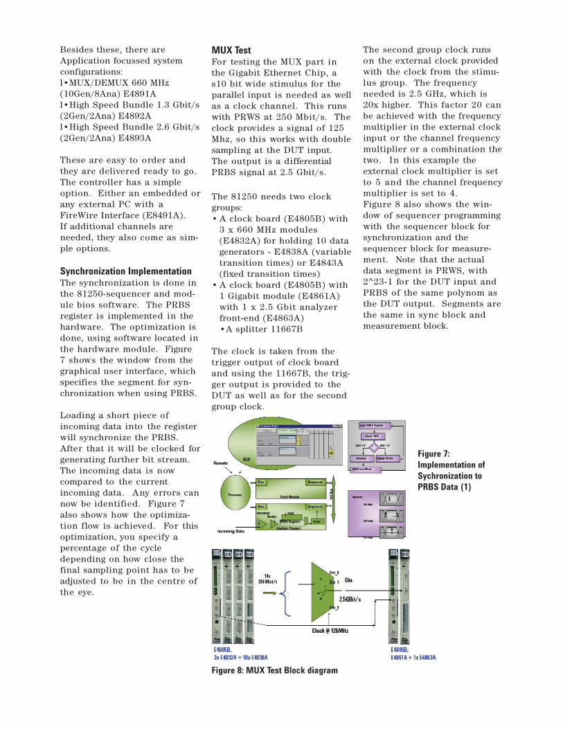
Synchronization ImplementationThe synchronization is done inthe 81250-sequencer and mod-ule bios software. The PRBSregister is implemented in thehardware. The optimization isdone, using software located inthe hardware module. Figure7 shows the window from thegraphical user interface, whichspecifies the segment for syn-chronization when using PRBS.
Loading a short piece ofincoming data into the registerwill synchronize the PRBS.After that it will be clocked forgenerating further bit stream.The incoming data is nowcompared to the currentincoming data. Any errors cannow be identified. Figure 7also shows how the optimiza-tion flow is achieved. For thisoptimization, you specify apercentage of the cycledepending on how close thefinal sampling point has to beadjusted to be in the centre ofthe eye.
MUX TestFor testing the MUX part inthe Gigabit Ethernet Chip, as10 bit wide stimulus for theparallel input is needed as wellas a clock channel. This runswith PRWS at 250 Mbit/s. Theclock provides a signal of 125Mhz, so this works with doublesampling at the DUT input.The output is a differentialPRBS signal at 2.5 Gbit/s.
The 81250 needs two clockgroups:• A clock board (E4805B) with
3 x 660 MHz modules (E4832A) for holding 10 datagenerators - E4838A (variabletransition times) or E4843A (fixed transition times)
• A clock board (E4805B) with1 Gigabit module (E4861A) with 1 x 2.5 Gbit analyzer front-end (E4863A)•A splitter 11667B
The clock is taken from thetrigger output of clock boardand using the 11667B, the trig-ger output is provided to theDUT as well as for the secondgroup clock.
The second group clock runson the external clock providedwith the clock from the stimu-lus group. The frequencyneeded is 2.5 GHz, which is20x higher. This factor 20 canbe achieved with the frequencymultiplier in the external clockinput or the channel frequencymultiplier or a combination thetwo. In this example theexternal clock multiplier is setto 5 and the channel frequencymultiplier is set to 4.Figure 8 also shows the win-dow of sequencer programmingwith the sequencer block forsynchronization and thesequencer block for measure-ment. Note that the actualdata segment is PRWS, with2^23-1 for the DUT input andPRBS of the same polynom asthe DUT output. Segments arethe same in sync block andmeasurement block.
Figure 7:Implementation ofSychronization toPRBS Data (1)
Figure 8: MUX Test Block diagram

DEMUX Test
For testing the DEMUX part inthe Gigabit Ethernet Chip, theopposite configuration is need-ed:One 2.5Gbit serial bitstreamgoes into the analyzer and theanalysis is performed with 10analyzer channels running at250Mbit/s.Again, a clock is needed at125Mhz. The clock groupresponsible for the serial signalprovides this. In addition, asecond generator is neededwhich operates the 125 MHzclock with a data pattern,which repeats 1's 10 times, fol-lowed by 0's 10 times. Thissignal is supplied as a clockonce again to the DUT and theanalyzer system by means ofthe splitter.
The following configuration ofthe Agilent 81250 is recom-mended:
• A clock board (E4805B) with1 x Gigabit module (E4861A)with 2 x 2.6Gbit Generator Front-Ends (E4862A)
• A clock board (E4805B) with3 x 660MHz modules (E4832A) with 10 660MHz Analyzer Front-Ends (as these come as pairs, 5x E4835A is needed)
• A splitter 11667B
The analyzer clock group runsat 250MHz. This is set to theexternal clock with a frequencymultiplier set to the value of 2.This is achieved with a clockgiven at 125MHz.
Figure 9: DEMUX Test BLock Diagram
Figure 10: Differential Input architecture

Differential InputsThe Agilent 81250 offers differ-ential inputs: this is accordingto the trend that higher speedsignals are transmitted withdifferential techniques. So itprovides input and complemen-tary input. This makes thetransmission less sensitive toESD and EMC.
The tolerance to common modeis much better than to singleended signals. Using a differ-ential input it is necessary toselect between a differential ora center tapped termination.Differential termination is a100-Ohm resistor between thetwo 50-Ohm inputs. Centertapped uses 2 50-Ohm resis-tors, which are connected to avoltage source, acting as termi-nation voltage.
ECL technology would requirecenter tapped mode with -2Vas termination voltage. LVDSwould work fine with differen-tial termination.
Measurement mode is inde-pendent of termination. Thereare three comparators, whichallow signal comparison as:
• Differential, between input and complementary input
• Single ended normal, normal input vs. threshold
• Single ended inverted, complementary input vs. threshold
The single ended modes arenecessary to verify each indi-vidual DUT output to bechecked for proper function.In case one output gets stuck,the other can still run a prop-er test with the differentialmeasurement mode. So it isnecessary to verify each outputagainst each threshold once.
Differential outputsSimilar issues occur for out-puts: If DUT gets faster, itneeds more and more comple-mentary signals for driving.This can be achieved by usingtwo channels. However, itwould be more economic touse one channel, which pro-vides both signals. It is alsoimportant that switching occursat the same point in time.
Again, the termination modelcan be selected for outputs.The reason for this is to com-pensate for the programmingvalues for levels, which woulddiffer with one or otherloading.
CharacterizationFor characterization, the CSC(E4874A) Software can beused. This provides predefinedmeasurement solutions for:• Eye diagram• Jitter• Schmoo plot
SONET OC-192 and SDH STM-64TestingTesting at 10Gbit is possible inconjunction with 12 Gbit BERtest equipment 76112A.
The 81250 delivers 16 channelswith PRWS 2^n-1 at 633Mbit/s.Together with a clock channel,the DUT makes this up to10Gbits. So the analysis cannow be done with 76112 BERtester or communication analyzer.
Figure 11: Differential Output architecture
Figure 12: Eye Diagram of a 1.25 Gbit Gigabit Ethernet Transmitter
Figure 13: Test setup for MUX 622 MHz to 10 Gbit/s
Related literature Publication number• Agilent 81250 Parallel 5968-9188E
Bit-Error Rate TesterProduct Overview
• Need to test BER? Complete Solutions 5968-9250Efor high speed digital transmissionsBrochure
For more information, please visit us www.agilent.com/find/parbert
Agilent Technologies’ Test and Measurement Support,Services, and AssistanceAgilent Technologies aims to maximize the value youreceive, while minimizing your risk and problems. We strive to ensure that you get the test and measurementcapabilities you paid for and obtain the support you need.Our extensive support resources and services can help you choose the right Agilent products for your applicationsand apply them successfully. Every instrument and systemwe sell has a global warranty. Support is available for atleast five years beyond the production life of the product.Two concepts underlie Agilent’s overall support policy:“Our Promise” and “Your Advantage.”
Our PromiseOur Promise means your Agilent test and measurementequipment will meet its advertised performance and functionality. When you are choosing new equipment, wewill help you with product information, including realisticperformance specifications and practical recommendationsfrom experienced test engineers. When you use Agilentequipment, we can verify that it works properly, help withproduct operation, and provide basic measurement assis-tance for the use of specified capabilities, at no extra costupon request. Many self-help tools are available.
Your AdvantageYour Advantage means that Agilent offers a wide range ofadditional expert test and measurement services, whichyou can purchase according to your unique technical andbusiness needs. Solve problems efficiently and gain a competitive edge by contracting with us for calibration,extra-cost upgrades, out-of-warranty repairs, and onsiteeducation and training, as well as design, system integra-tion, project management, and other professional engineer-ing services. Experienced Agilent engineers and techni-cians worldwide can help you maximize your productivity,optimize the return on investment of your Agilent instru-ments and systems, and obtain dependable measurementaccuracy for the life of those products.
Agilent T&M Software and ConnectivityAgilent’s Test and Measurement software and connectivityproducts, solutions and developer network allows you totake time out of connecting your instruments to your com-puter with tools based on PC standards, so you can focuson your tasks, not on your connections. Visit www.agilent.com/find/connectivityfor more information.
For more information on Agilent Technologies’ products,applications or services, please contact your localAgilent office. The complete list is available at:
www.agilent.com/find/contactusProduct specifications and descriptions in this document subject to change without notice.
© Agilent Technologies, Inc. 2003, 2004Printed in USA, August 04, 20045968-9695E
Phone or Fax
United States:(tel) 800 829 4444(fax) 800 829 4433Canada:(tel) 877 894 4414(fax) 905 282 6495China:(tel) 800 810 0189(fax) 800 820 2816Japan:(tel) (81) 426 56 7832(fax) (81) 426 56 7840
Korea:(tel) (080) 769 0800(fax) (080)769 0900Latin America:(tel) (305) 269 7500Taiwan:(tel) 0800 047 866 (fax) 0800 286 331Other Asia PacificCountries:(tel) (65) 6375 8100 (fax) (65) 6755 0042Email: [email protected]
www.agilent.com/find/emailupdatesGet the latest information on the products and applications you select.
Product specifications and descriptions in this document subject to changewithout notice.
For the latest version of this document, please visit our website at www.agilent.com/find/tmdir and go to the Key Library Information area orinsert the publication number (5968-9695E) into the search engine.