Embed Size (px)
Citation preview

Agilent AN 1314
Testing and Troubleshooting Digital RF CommunicationsReceiver Designs Application Note
I
Q
Wireless Test Solutions

3
This application note presents the fundamentalmeasurement principles involved in testing and trou-bleshooting digital RF communications receivers—particularly those used in digital RF cellular systems.Measurement setups are explained for the variousreceiver tests, and troubleshooting tips are given.
The demand for ubiquitous wireless communica-tions is challenging the physical limitations of cur-rent wireless communications systems. Wirelesssystems must operate in a very limited area of theradio spectrum and not interfere with other systems.The maturing wireless markets are becoming muchmore competitive, and product cycle times are nowmeasured in months instead of years. Consequently,network equipment manufacturers must producewireless systems that can be quickly deployed andprovide bandwidth-efficient communications.
Digital modulation has several advantages overanalog modulation. These include bandwidth effi-ciency, superior immunity to noise, low power con-sumption, privacy, and compatibility with digitaldata services. These advantages, coupled withadvances in digital signal processing and in analog-to-digital conversion, have spawned the currentmigration to digital RF communications formats.
Digital RF communications systems use complextechniques to transmit and receive digitally modu-lated signals through the radio channel. Thesecomplexities challenge designers in the isolation of system problems. Signal impairments can betraced back to a component, device, or subsystemof the digital RF communications system. Success-ful receiver design depends on the ability to locate sources of error.
The digital radio receiver must extract highly vari-able RF signals in the presence of interference andtransform these signals into close facsimiles of theoriginal baseband information. Several tests verifyreceiver performance in the presence of interferingsignals. These performance verification tests arecategorized as either in-channel or out-of-channelmeasurements.
This application note includes:
• A block diagram of a digital radio communica-tions system.
• Common receiver designs.• In-channel tests, including sensitivity and
co-channel immunity.• Out-of-channel tests, including spurious and
intermodulation immunity and adjacent andalternate channel selectivity.
• Best practices in the receiver performance tests.• Troubleshooting techniques for receiver designs.• An appendix that relates Bit Error Rate (BER)
to Error Vector Magnitude (EVM).
The setups required to perform the receiver performance tests are included in this applicationnote along with descriptions of potential errors in the measurement process. Troubleshooting techniques applicable to the design of digital radio receivers are also provided.
Introduction

5667889
101010131415161617182223
242425252729293132
33
34
37
38
Table of Contents
Introduction
1. Digital Radio Communications Systems1.1 Digital radio transmitter1.2 Digital radio receiver
1.2.1 I/Q demodulator receiver1.2.2 Sampled IF receiver1.2.3 Automatic Gain Control (AGC)
1.3 Filtering in digital RF communications systems
2. Receiver Performance Verification Measurements2.1 General approach to making measurements2.2 Measuring Bit Error Rate (BER) 2.3 In-channel testing
2.3.1 Measuring sensitivity at a specified BER 2.3.2 Verifying co-channel rejection
2.4 Out-of-channel testing 2.4.1 Verifying spurious immunity2.4.2 Verifying intermodulation immunity2.4.3 Measuring adjacent and alternate channel selectivity
2.5 Fading tests2.6 Best practices in conducting receiver performance tests
3. Troubleshooting Receiver Designs 3.1 Troubleshooting steps3.2 Signal impairments and ways to detect them
3.2.1 I/Q impairments 3.2.2 Interfering tone or spur3.2.3 Incorrect symbol rate 3.2.4 Baseband filtering problems3.2.5 IF filter tilt or ripple
3.3 Table of impairments versus parameters affected
4. Summary
5. Appendix: From Bit Error Rate (BER) to Error Vector Magnitude (EVM)
6. Symbols and Acronyms
7. References

5
The digital radio signal experiences many transfor-mations in its migration from a baseband signal atthe transmitter to its replication at the receiver. Arudimentary block diagram of a digital radio com-munications system (Figure 1) reveals the transfor-mation process the signal undergoes from origina-tion to reception.
The system-level diagram in Figure 1 displays thesymmetry of the digital radio. To a certain degree,the receiver can be considered a reverse implemen-tation of the transmitter. Consequently, the meas-urement challenges are similar for both parts ofthe digital radio system. However, unique problemsexist at various locations in the system. For exam-ple, the receiver must detect weak signals in thepresence of noise and is therefore tested with verylow level signals. The transmitter must not inter-fere with other radio systems and is consequentlytested for the amount of interference it producesin the nearby frequency channels.
Certain parts of the digital radio may be imple-mented in a Digital Signal Processor (DSP), anApplication-Specific Integrated Circuit (ASIC), or a Digital Down Converter (DDC). The DSP, ASIC,or DDC has different levels of involvement in thevarious digital radio designs. Sometimes it is diffi-cult to distinguish those problems originating inthe digital portion of the radio from those originat-ing in the analog portion. This application notedescribes how to isolate and clarify sources oferror in digital radio receiver tests and designs.
1. Digital Radio Communications Systems
SymbolEncoder
Input(Data or Voice)
Channel Coding/Interleaving/Processing
Amplifier
Power Control
RF LO
UpconverterBaseband
Filter IF FilterI
Q
I/QModulator
IF LO
I
Q
IF Filter
DemodulatorOutput
(Data or Voice)
Low-NoiseAmplifier with
AutomaticGain Control
PreselectingFilter
BitDecoder
BasebandFilterI
Q
I
Q
Channel
IF LORF LO
Transmitter
Receiver
Downconverter Downconverter
Figure 1. Block diagram of a digital radio system

6
1.1 Digital radio transmitterThe digital radio transmitter (see Figure 1) acceptsa baseband waveform and translates that signalinto a waveform that it can effectively transmitthrough the channel. Before the transformationfrom baseband to a Radio Frequency (RF) channel,the waveform is digitized to utilize the advantagesof digital modulation. Coding is applied to the sig-nal to more efficiently use the available bandwidthand to minimize the effects of noise and interfer-ence that will be introduced by the channel. Thecoded signal is filtered, modulated, and changedback to an analog waveform that is converted tothe desired frequency of transmission. Finally, the RF signal is filtered and amplified before it istransmitted from the antenna. A more detaileddescription of digital transmitters can be found in the companion Agilent Technologies applicationnote, Testing and Troubleshooting Digital RFCommunications Transmitter Designs [1].
1.2 Digital radio receiverThe digital radio receiver (Figure 2) can be imple-mented several ways, but certain components existin all receivers. The receiver must extract the RF signal in the presence of potential interference.Consequently, a preselecting filter is the first com-ponent of the receiver, and it attenuates out-of-band signals received by the antenna. A Low-NoiseAmplifier (LNA) boosts the desired signal levelwhile minimally adding to the noise of the radiosignal. A mixer downconverts the RF signal to alower Intermediate Frequency (IF) by mixing theRF signal with a Local Oscillator (LO) signal. TheIF filter attenuates unwanted frequency compo-nents generated by the mixer and signals fromadjacent frequency channels. After the IF filter, thevariations in receiver design manifest themselves.
Of the many different ways to implement a digitalradio receiver, most designs fall into two basic categories: I/Q demodulation and sampled IF.
IF Filter
LO
Demodulatorand Decoder
Output (Data or
Voice)Low-Noise
Amplifier with Automatic
Gain Control
PreselectingFilter Downconverter
Figure 2. Receiver block diagram

7
1.2.1 I/Q demodulator receiverI/Q demodulation implemented with analog hard-ware is a commonly used digital radio receiverdesign. The function of the analog I/Q demodulator(Figure 3) is to recover the baseband I and Q symbols.
After downconversion to the IF, the signal is separated into two distinct paths. To convert tobaseband, each path is mixed with an LO whosefrequency equals the IF frequency. The upper-path signal (I) is simply mixed with the LO andthen filtered. In the lower path, a 90° phase shift is introduced in the mixing signal. This lower-path signal (Q) is converted to baseband by mixingwith the phase-shifted LO signal, and then filtered.This process produces the in-phase (I) and out-of-phase (Q) baseband components of the datastream. For a detailed explanation of I/Q modula-tion, consult [2].
Although the I/Q demodulator receiver is a popu-lar design, it has potential problems. Unequal gainin the I and Q paths and/or a relative phase shiftother than 90° (quadrature error) will cause imagesuppression problems in the baseband mixers. (Formore information on image suppression, see [3].)I/Q demodulators inherently produce a spuriousresponse at DC (that is, in the center of the pass-band) regardless of the input frequency. As a result,I/Q demodulators are most commonly used in sin-gle-channel base station receivers that have a sepa-rate receiver for each frequency channel, ratherthan in multi-channel base station receivers thatuse a single, wide-bandwidth receiver for the entireband of frequencies.
The I and Q data streams are sampled by Analog-to-Digital Converters (ADCs). This allows filteringand signal corrections to be performed with digitalsignal processing. Baseband filtering by a DSP,ASIC, or DDC removes many of the problems asso-ciated with analog filter implementations (for exam-ple, phase and group delay problems) and providesfilter characteristics closer to ideal than those ofanalog filters. Baseband filtering, whether it is ana-log or digital, is better behaved than IF filtering.
IF Filter
LO
Low-NoiseAmplifier
PreselectingFilter
BasebandFilter
ADC I
Q
BasebandFilter
ADC
LO
90-Degree Phase Shifterφ
Mixer
Mixer
Downconverter
Figure 3. I/Q demodulator

8
1.2.2 Sampled IF receiverTo decrease analog hardware complexity, the digi-tally modulated signal can be sampled earlier inthe signal path, which increases the digital or soft-ware complexity of the receiver design. The sam-pled IF receiver converts the analog signal to a digital data stream earlier than the I/Q demodula-tor does (see Figure 4).
In this receiver, the IF signal is digitized. The sampled data stream from the ADC is digitallydemodulated into its I and Q components, and the original signal is reconstructed.
This type of receiver is becoming more popularbecause of advances in ADCs and DSPs. The sam-pled IF receiver design requires less analog hard-ware than the I/Q demodulator type and does notsplit the analog signal into two paths. The I/Qdemodulation is actually performed in a DSP, ASICor DDC. Digital I/Q demodulation avoids phase and amplitude imbalance between I and Q signals.The tradeoff is more digital signal processing andpower-hungry ADCs fast enough to capture all the information in the analog signal (two factorsthat reduce battery life in mobile phones). As withthe I/Q demodulator, the sampled IF receiverrequires a downconverter that does not degradethe incoming signal.
1.2.3 Automatic Gain Control (AGC) AGC is used in digital radio receivers to handle the wide range of signal levels encountered at thereceiving antenna. AGC compresses the signalrange by reducing the gain of the IF, and some-times the RF, stages as the signal level increases. A strong RF signal can overdrive the mixer andcause excessive signal distortion. The receivermust also process weak RF signals in the presenceof noise. Therefore, the RF portion of the receivermay incorporate AGC to process the full range ofsignal levels presented to it. Used in the IF stage,AGC can prevent overload and maintain a reason-ably constant signal input to the demodulatorstage. For all applications, the AGC circuitry mustmaintain allowable levels of signal distortion overa broad range of power levels. Also, the AGCshould respond quickly to signal level changes as it processes signals over its entire dynamic range.
Figure 4. Sampled IF receiver
IF Filter
LO
Low-NoiseAmplifier
PreselectingFilter
ADC
Downconverter

9
1.3 Filtering in digital RF communications systemsDistortion-free transmission of the digital I and Qsignals theoretically requires infinite bandwidth.An infinite-bandwidth RF communications systemwould interfere with other systems and would notprovide efficient use of radio spectrum. Filteringnarrows the bandwidth of RF systems, but it alsoslows down signal transitions.
Baseband filtering rounds off the rapid transitionsin the transmitted data, but this can cause Inter-Symbol Interference (ISI). A Nyquist filter, which is a type of raised-cosine filter, minimizes ISI byforcing the filter’s impulse response to zero at thesymbol points (except at the center of the filter).Thus, the time response of the Nyquist filter(Figure 5) goes through zero with a period thatexactly corresponds to the symbol spacing. Adjacentsymbols do not interfere with each other at thesymbol times because the response equals zero atall symbol times except the desired one.
The sharpness of a raised-cosine filter is describedby its alpha (a) and quantifies the occupied band-width of the signal. An ideal (“brick wall”) filterwould have an alpha of zero. Typical alpha valuesrange from 0.35 to 0.5. Filter alphas also affecttransmitted power. A low alpha value results inlow occupied bandwidth but requires high peaktransmit power. Consequently, the filter alpha mustbe carefully chosen to achieve a balance betweenspectral occupancy and required transmit power.In some systems, a root-raised-cosine filter is imple-mented at both ends of the digital radio, and theresulting overall filter response is a raised cosine.
Gaussian filters, such as those used in GSM sys-tems, do not provide the theoretical zero ISI likethe Nyquist filters do. The Gaussian filter has aGaussian shape in the time and frequency domains,and it does not go to zero at the symbol spacing.This causes some ISI, but each symbol interactssignificantly with only the preceding and succeed-ing symbols. The bandwidth-time product (BT) ofthe Gaussian filter corresponds to the alpha of theNyquist filter, and typical BT values range from 0.3to 0.5. Unlike Nyquist filters, Gaussian filters arenot split into matched pairs in the transmitter and receiver. They are only used in the transmitter.GSM receivers typically use Butterworth filtersthat have a sharper roll-off than the Gaussian fil-ters. Consequently, sensitivity is improved becauseless out-of-channel noise and interference is allowedinto the receiver’s passband.
A more thorough examination of filtering is provided in [2].Figure 5. Impulse response of a Nyquist filter
-10 -5 0 5 10ti
0
1
0.5hi
Symbol Period

10
This section contains test setups and proceduresfor performance tests on digital radio receivers.Each receiver must meet strict performance criteriadefined by the various standards of the telecom-munications industry’s governing bodies (the ITU,ETSI, TIA, and others). Design teams must developperformance criteria for their receiver, or for aportion of that receiver, and conduct unique per-formance tests to verify correct implementationand modeling of components in the receiver. More-over, these performance tests verify receiver compliance prior to the design’s submission fortype approval.
Performance verification tests are divided into in-channel and out-of-channel measurements. In-channel measurements test the receiver’s opera-tion within the frequencies occupied by the desiredsignal. Out-of-channel measurements verify thatthe receiver is not being adversely affected by (or affecting) other signals outside its specific fre-quency channel. Although the performance testspresented in this application note focus on digitalRF cellular applications, many of the concepts and tests apply to other forms of digital RF com-munications.
2.1 General approach to making measurementsThe most comprehensive receiver test is to evalu-ate the reconstructed baseband signal that has beenprocessed by the receiver. In this test, one piece oftest equipment stimulates the antenna port of thereceiver and is considered to be an ideal transmit-ter. Another instrument monitors the demodulateddigital bit stream. If desired, impairments can beintroduced by inserting interference in the channelbetween the source and the receiver, or by alteringparameters in the source, to determine the receiver’sability to operate properly under less-than-idealconditions.
The following tests assume the receiver is complete.If the digital portion of the receiver is unavailablefor testing (for example, if it’s still under develop-ment), then the analog RF designer needs to estab-lish performance goals for the analog portion of thereceiver. Typical performance goals are the estimatedoptimum noise figure for the receiver to pass theperformance verification tests and the estimatedoptimum Signal-to-Noise Ratio (SNR) for properADC operation (at the digital conversion point).
2.2 Measuring Bit Error Rate (BER)BER is the fundamental measurement used whentesting receiver performance parameters such assensitivity and selectivity. It is the percentage oferroneous bits received compared to the total num-ber of bits received during an observation period.Virtually all BER test instruments use a Pseudo-Random Binary Sequence (PRBS) as the test sig-nal. PRBS signals are usually labeled PNx, where x is the number of bits being permutated in thesequence (for example, PN9 = 29–1 or 511 bits).Since an entire PNx sequence can be reconstructedfrom any sequence of “x” bits, using a PRBS signaleliminates the need to synchronize the receivedand transmitted bits. Alternatively, the entirePRBS is reconstructed in the BER tester (BERT)receiver from the first correct “x” bits received.The received signal is then compared to the recon-structed correct bit sequence. (For a thoroughexplanation of BER testing, see [4]).
2. Receiver Performance Verification Measurements

11
Two popular methods exist for BER testing ofmobile phones: baseband BER and loopback BER.The feature set of the unit-under-test (UUT) dictateswhich test method to use. For the baseband BERtest, the demodulated PRBS signal at the receiver
remains at baseband and is compared to the recon-structed PRBS by the BERT (see Figure 6). Typically,PDC and PHS mobile phones and subassembliesuse the baseband BER measurement method.
Figure 6. Baseband BER test configuration
Comparator
Encoder
PatternGenerator
RF SignalSource
RF Signal
Decoder
Baseband Signal00110110110001
BasebandModulator
(Option UN3/UN4/UN8)
Bit ErrorRate Tester
(Option UN7)
Agilent ESG-D SeriesSignal Generator

12
Conversely, for the loopback BER test the receivedsignal is retransmitted, or looped back to a receiver(Figure 7). In the loopback test, the UUT demodu-lates the incoming RF signal, decodes it, then re-encodes the data stream (with possible errors),and retransmits the signal, often to the originaltransceiver. To attain the BER, this received signalis compared to the expected PRBS that is recon-structed by the BERT (see [4]). GSM handsets aretested using the loopback method.
The Agilent ESG-D signal generator can be config-ured to provide the RF signal that carries the PRBSand perform the BER measurement.
Data is managed in telecommunications systems by a hierarchical system of bit grouping. Speechframes are nearly the lowest-level building blocksin this hierarchical system. Not all bits in a speechframe are equally important. Some bits are soimportant that the entire frame is erased if any ofthem are bad. This leads to a new parameter forexpressing receiver performance—Frame ErasureRate (FER). It is the percentage of erased framescompared to the total number of frames sent dur-ing an observation period. Frame erasure alsoleads to a modification of our BER measurement.When frames are erased, only the BER of theremaining frames is measured. This parameter is called residual BER (RBER).
Figure 7. Loopback BER test configuration
Comparator
Encoder
PatternGenerator
RF SignalSource
PRBS
RF Signal
Decoder
RF SignalReceiver
BERT
RF Signal

13
2.3 In-channel testing The most significant in-channel test measures thesensitivity of the receiver. Sensitivity specifies theminimum signal level for a specified percentage of errors in the demodulated information. As the separation between transmitter and receiverincreases, or as fading occurs in the radio channel,the signal will drop into the noise floor from theperspective of the receiver. Information will be lostwhen the signal approaches the noise floor. Theability of the receiver to capture the information ina signal as it drops to very low levels is a functionof the receiver’s sensitivity. The go/no-go methodfor sensitivity testing is to stimulate the receiverwith a very accurate signal set to a relatively lowpower level and see if the receiver output is accept-able. Alternatively, the signal level is adjusted for a specified SNR or other performance metric. Foranalog FM receivers, the performance metric isknown as SINAD (12 dB is typical). SINAD is theratio of signal-plus-noise-plus-distortion to thenoise-plus-distortion at the same output. Similarly,for digital receivers the specified performance metric is the BER or FER.
Figure 8. Understanding SINADThe top curve in Figure 8 is the desired audio output of the receiver. As the RF input to the receiver is reduced, this curve falls off. The bottom curve is the residual humand noise of the receiver. As the RF input is reduced, theAGC of the receiver adds gain, which increases the residualhum and noise. SINAD is the difference between these two curves. The level of RF input required to maintain aSINAD of 12 dB is generally defined as the sensitivity of an FM receiver.
12 dB SINAD
Desired Audio Signal
Residual Hum & Noise
RF Input to Receiver (µV)Au
dio
Outp
ut o
f Rec
eive
r (dB
)

14
Co-channel immunity testing is similar to sensitivitytesting. The level of signal distortion is monitoredwith an interfering signal present in the same RFchannel. The interfering signal may be ContinuousWave (CW), narrowband, or of the same type as thedesired signal. The ability of the receiver to remainsensitive to the desired signal while subjected tothe interfering signal is a measure of its co-channelimmunity.
2.3.1 Measuring sensitivity at a specified BERSensitivity is one of the key specifications for adigital radio receiver and is specified at a particu-lar BER (or FER). Sensitivity is the minimumreceived signal level that produces a specified BER when the signal is modulated with a bitsequence of data.
Because sensitivity is often expressed in voltageunits, such as mV, the following equation will beused to convert to dBm:
dBm = 10 * log (Vrms2/Zo) + 30
where Vrms = receiver sensitivity in volts rms Zo = receiver impedance (typically 50Ω).
For example, if a receiver has a sensitivityexpressed as 1 µV, the sensitivity can be convertedto –107 dBm for a system with a 50Ω impedance.
To perform the sensitivity test, connect a signalsource to the antenna port of the receiver with acable of known loss. Then connect the output ofthe receiver to the BERT. See Figure 9.
If the approximate sensitivity is unknown, the signal level should be set to a nominal level (suchas –90 dBm) and decreased until the specified BER occurs. The sensitivity is the power level ofthe signal minus the loss in the cable. For example,if the signal generator is transmitting a –106 dBmsignal when the specified BER is reached and thecable loss is 4 dB, then the sensitivity is –110 dBmfor the receiver.
Figure 9. Sensitivity measurement setup
Signal Generator
BERT
Data
DUT
Modulated RF Signal
Agilent ESG-D

15
2.3.2 Verifying co-channel rejectionMost receivers are required to maintain a specifiedBER in the presence of an interfering signal withinthe channel. Frequently, this co-channel interferingsignal will be a CW signal. Figure 10 illustrates the test setup for the co-channel rejection measure-ment. This setup includes a power combiner thathas some power loss associated with it. Maximuminsertion loss of most 2-way resistive combiners isnear 6 dB when combining two noncoherent signalssuch as in this test. For all measurements using apower combiner, the combiner loss should be char-acterized and offset by an increase in signal powerfrom the signal generators.
The frequency of the desired signal, a digitallymodulated test signal, is set to the center of thepassband of the receiver. The power of this signalis typically set to a level relative to the measuredsensitivity of the receiver (for example, 3 dB above).The frequency of the interfering signal is set withinthe passband of the receiver. The power level of the interfering signal is set to a nominal level atwhich the BER of the receiver must not exceed thespecified level. The required BER level is usuallythe same level specified for the receiver sensitivitymeasurement. The difference in power levelsbetween the two signals is the interference ratio.
For example, suppose a 931.4375 MHz pager has a sensitivity of –105 dBm with a BER of 3%. Thedesired signal is set to 931.4375 with a power levelof –102 dBm. At this power level the BER is lessthan 3%. The channel width for the pager is 25 kHz.The interfering signal is set to 931.4380 MHz. Thepower level of the interfering signal is first set to–105 dBm and gradually increased until the BER is again 3%. If a level of –97 dBm is required toreturn the BER to 3%, then the co-channel rejec-tion is 5 dB.
Figure 10. Co-channel rejection measurement setup
Data
In-band CW orModulated RF Signal
(Interfering)
DUT
Combiner
Modulated RF Signal (Desired)
Σ
Agilent ESG-D With BERT
Signal Generator
Signal Generator
Agilent ESG-D

16
2.4 Out-of-channel testing Out-of-channel, or blocking, tests verify correctreceiver operation in the presence of out-of-channelsignals and monitor the receiver’s susceptibility to internally generated spurious responses. Threeprominent out-of-channel tests verify receiver per-formance: spurious immunity, intermodulationimmunity, and adjacent/alternate channel selectivity.For certain digital formats, the single-tone blockingtest verifies receiver performance with a large signal in a nearby frequency channel. A large sin-gle tone slightly offset from the carrier frequencycould desensitize a receiver to the desired signal.The single-tone blocking test is straightforwardand will not be covered in this application note.
Spurious immunity is the ability of the receiver toprevent single, unwanted signals from causing anundesired response at the output of the receiver.Spurious immunity is similar to co-channel immu-nity, but the interfering signals occur across abroad range of frequencies instead of in-channel.
Intermodulation immunity tests for distortionproducts that are generated when more than onetone is present at the input of the receiver. In thistest, two interfering signals are combined with thedesired signal at the input of the receiver. The fre-quencies of the interfering signals are set such thatone of the third-order intermodulation productslies within the passband of the receiver. The powerof these interferers is raised until the sensitivity of the receiver is compromised.
Adjacent channel selectivity measures the ability of the receiver to process the desired signal with a strong signal in the adjacent channel. Alternatechannel selectivity is a similar test in which theinterfering signal is two RF channels away fromthe passband of the receiver.
2.4.1 Verifying spurious immunitySpurious responses, also called spurs, manifestthemselves in radio receivers in two ways: they aregenerated internally by the receiver, or they resultfrom the interaction of the receiver with externalsignals. Both types of spurs should be identified.Replacing the antenna of the receiver with a loadwill ensure that the receiver is not picking up any stray signals. Connect the final analog outputof the receiver to a spectrum analyzer. Any spurviewed on the spectrum analyzer is internally gen-erated by the receiver and may be a harmonic ofthe power supply, a harmonic of the system clock,or a spur from an LO.
Spurious response immunity is a measure of thereceiver’s ability to prevent single, unwanted sig-nals from causing an undesired response at theoutput of the receiver. Prior to making this meas-urement, the internally generated spurs must be identified (as described above) and should bebelow the specified level. To perform the spuriousimmunity measurement, one signal generator supplies a modulated test signal in the desired RF channel at a level above the sensitivity of thereceiver (usually 3 dB above). The second signalgenerator supplies an interfering signal. This inter-fering signal is adjusted to several frequencies to verify the receiver’s immunity to spurs. Refer to Figure 11.

17
The interfering signal may be modulated or unmod-ulated, depending upon the frequency range andthe communications standard. The output ampli-tude of the interfering signal is set at a specificlevel at which the BER of the receiver under testmust be less than a specified level (usually theBER specified in the sensitivity test). The ampli-tude difference between the test signal and theinterfering signal is the spurious immunity (SI) of the receiver:
SI = Pint – Ptest (dB)
Spurs from the signal generator used to providethe interfering signal can cause a good receiver toappear bad. Any spurs created by the interferingsignal generator should be less than the receiver’sspurious immunity.
2.4.2 Verifying intermodulation immunityIntermodulation products may be generated withinthe receiver when more than one signal is presentat the input of the receiver. Intermodulation prod-ucts are caused by receiver non-linearities. Two-tone intermodulation is a common method of test-ing a receiver. The test signal is the same signalused in other measurements (for example, spuri-ous immunity). The frequencies of the interferingsignals are set such that one of the third-orderintermodulation products (frx1 = 2f1 – f2 and frx2 =2f2 – f1) falls within the passband of the receiver.See Figure 12.
Figure 11. Spurious immunity measurement setup
Data
DUT
Combiner
Modulated RF Signal (Desired)
Σ
Agilent ESG-D With BERT
Signal Generator
Signal Generator
Agilent ESG-D
Out-of-band CW orModulated RF Signal
(Interfering)
f1
f2
frx1=2f1– f2frx2=2f2– f1
frx1 frx2
f1 f2
f1 f2 Low-NoiseAmplifier
PreselectingFilter
Antenna
IF Filter
LO
Figure 12. Intermodulation products

18
The power levels of the interfering signals are setequal to each other at a specified level, and theBER of the desired signal is checked. As with otherreceiver tests, the required BER level is usually the BER at which the sensitivity is measured.
Whenever two signals are input to a combiner, thenonlinearities of the signal generators may createintermodulation products (see Figure 13). Thereare several techniques for reducing signal genera-tor intermodulation products:
1) maintain a frequency separation between theinterfering signals that is greater than the band-width of the Automatic Level Control (ALC) of thesources; 2) add attenuators to the outputs of thesignal generators; 3) use hybrid combiners; 4) useisolators; and 5) turn off the ALC of the sources.
All these techniques may be applied simultaneouslyto reduce intermodulation products. Maintaining a large frequency separation is usually the mosteffective means to combat this problem. For exam-ple, if the ALC bandwidth is 1 kHz, the signal sepa-ration should be at least 10 kHz. If this cannot bedone, adding attenuation at the signal generatoroutputs theoretically reduces the intermodulationproducts 3 dB for every 1 dB of attenuation.
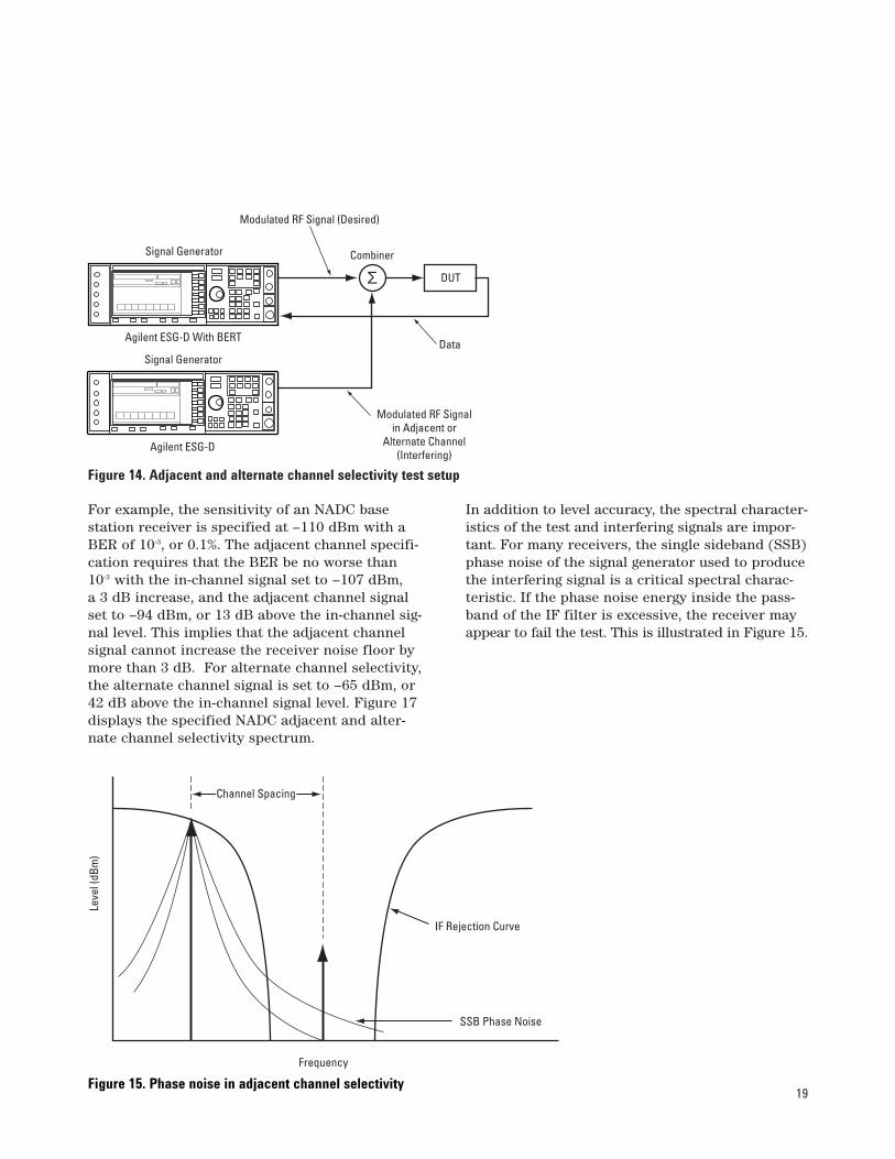
2.4.3 Measuring adjacent and alternate channel selectivityAdjacent and alternate channel selectivity measurethe receiver’s ability to process a desired signalwhile rejecting a strong signal in an adjacent chan-nel (one channel away) or alternate channel (usu-ally two channels away). The selectivity tests arevery important for communications receivers inwhich channel spacings are narrow and adjacentand alternate channel power is hard to control (forexample, Specialized Mobile Radio, or SMR). Anadjacent and alternate channel selectivity test setupis shown in Figure 14. One signal generator inputsa test signal at the desired channel frequency at alevel relative to the sensitivity of the receiver (usu-ally 3 dB above). The second signal generator inputseither the adjacent channel signal, offset by onechannel spacing, or the alternate channel signal,offset by two channel spacings. The out-of-channelsignal is set to a specified level at which the BERof the test signal is below a certain rate (usuallythe same level specified in the sensitivity test).
Figure 13. Intermodulation immunity measurement setup
Data
Out-of-band CW orModulated RF Signals
(Interfering)
DUT
CombinerModulated RF Signal (Desired)
Σ
Agilent ESG-D With BERT
Signal Generator
Signal Generator
Agilent ESG-D
Signal Generator
Agilent ESG-D
19
For example, the sensitivity of an NADC base station receiver is specified at –110 dBm with aBER of 10-3, or 0.1%. The adjacent channel specifi-cation requires that the BER be no worse than 10-3 with the in-channel signal set to –107 dBm, a 3 dB increase, and the adjacent channel signalset to –94 dBm, or 13 dB above the in-channel sig-nal level. This implies that the adjacent channelsignal cannot increase the receiver noise floor bymore than 3 dB. For alternate channel selectivity,the alternate channel signal is set to –65 dBm, or42 dB above the in-channel signal level. Figure 17displays the specified NADC adjacent and alter-nate channel selectivity spectrum.
In addition to level accuracy, the spectral character-istics of the test and interfering signals are impor-tant. For many receivers, the single sideband (SSB)phase noise of the signal generator used to producethe interfering signal is a critical spectral charac-teristic. If the phase noise energy inside the pass-band of the IF filter is excessive, the receiver mayappear to fail the test. This is illustrated in Figure 15.
Figure 14. Adjacent and alternate channel selectivity test setup
Data
DUT
Combiner
Modulated RF Signal (Desired)
Σ
Agilent ESG-D With BERT
Signal Generator
Signal Generator
Agilent ESG-D
Modulated RF Signalin Adjacent or
Alternate Channel(Interfering)
Figure 15. Phase noise in adjacent channel selectivity
Channel Spacing
Frequency
SSB Phase Noise
IF Rejection Curve
Leve
l (dB
m)

20
The required signal generator SSB phase noise maybe calculated from:
Fn = Pac – 10 * log(1/Be) + Pmar
where Fn = signal generator SSB phase noise (dBc/Hz) at the channel spacing offset
Pac = adjacent or alternate channel selectivity specification (dB)
Be = receiver noise-equivalent bandwidth (Hz)Pmar = test margin (dB)
Since Pac and Be are fixed by the specifications ordesign, the test margin determines the power thatthe signal generator phase noise will be allowed tocontribute to the IF passband of the receiver. Alarge test margin increases the confidence that thereceiver operates properly in the presence of SNRdegradation due to fading in the channel or due toimperfections in receiver components. For a systemusing a new technology or new operating frequen-cies, a large test margin should be used to compen-sate for uncertainties.
For a receiver with a noise-equivalent bandwidthof 14 kHz, a Pac at the adjacent channel of 70 dB, amargin of 10 dB, and a channel spacing of 25 kHz,the required SSB phase noise is –122 dBc/Hz at a 25 kHz offset. This is typical for an analog FMreceiver. Unlike the FM receiver in this example,most digital communications receivers have adja-cent channel selectivity values less than 15 dB.
For a GSM receiver with a noise-equivalent band-width of 200 kHz, a Pac at the adjacent channel of 9 dB, a margin of 10 dB, and a channel spacing of200 kHz, the required SSB phase noise is –72 dBc/Hzat a 200 kHz offset. The required SSB phase noiseis driven primarily by Pac.
Table 1 lists the values of adjacent and alternatechannel selectivity for various communicationssystems as well as the required signal generatorSSB phase noise. A 10 dB test margin was used.Clearly, for the digital RF communications formats,the signal generator SSB phase noise is not asimportant as for analog FM systems.
For selectivity tests the spectral shape of the signalis the special characteristic that is of primaryimportance. The digital modulation formats usedby GSM, CDMA, NADC, and PDC characteristicallyleak a small amount of power into the adjacentchannels. Figures 16–18 plot amplitude versus fre-quency for the selectivity values specified in Table 1.The impact of the spectral shape on the adjacentand alternate channels of the receiver is evident.To properly test your digital radio receiver, theAdjacent Channel Power (ACP) of your signal gen-erator must be below the required system specifi-cation plus the desired test margin.
System Channel Approximate Adjacent Maximum SSB Alternate Maximum SSBType Spacing Receiver Noise Channel Phase Noise Channel Phase Noise
Bandwidth Selectivity @ Offset Selectivity @ Offset
Analog FM 25 kHz 14 kHz 70 dB –122 dBc/Hz @ 25 kHz
GSM 200 kHz 200 kHz 9 dB –72 dBc/Hz @ 200 kHz 41 dB –104 dBc/Hz @ 400 kHz
NADC 30 kHz 35 kHz 13 dB –68 dBc/Hz @ 30 kHz 42 dB –97 dBc/Hz @ 60 kHz
PDC 25 kHz 33 kHz 1 dB –56 dBc/Hz @ 25 kHz 42 dB –97 dBc/Hz @ 50 kHz
Table 1. Maximum tolerable SSB phase noise

21
Figure 16. GSM adjacent and alternate channel selectivity spectrum
–44
–76
–85
fc +200 +400
Offset from Nominal Center Frequency (kHz)
Ampl
itude
(dBm
) 41 dB
9 dB
Figure 18. PDC adjacent and alternate channel selectivity spectrum
–65
–94
–107
fc +30 +60
13 dB
Offset from Nominal Center Frequency (kHz)
Ampl
itude
(dBm
) 42 dB
–58
–99–100
fc +25 +50
1 dB
Offset from Nominal Center Frequency (kHz)
Ampl
itude
(dBm
) 42 dB
Figure 17. NADC adjacent and alternate channel selectivity spectrum

22
2.5 Fading testsA unique challenge for the receiver is to overcomethe random effects of the radio channel. In a cellu-lar environment, a radio signal may take a numberof paths en route from the transmitter to the receiver.These multipath signals may add up constructively(in phase) or destructively (out of phase) at thereceiver as a function of the distance each signaltravels. The effect of this phenomenon can be fad-ing of the received signal strength, which cangreatly stress signal reception. Fast fading distortsthe shape of the baseband pulse. This distortion is linear and creates ISI. Adaptive equalizationreduces ISI by removing linear distortion inducedby the channel. Slow fading results in a loss ofSNR. Error-correction coding and receive diversityare used to overcome the effects of slow fading.
Fading tests can be performed by routing the testsignal through a radio-channel emulator such asthe Agilent 11759C RF channel simulator beforethe signal is processed by the receiver. This deviceprovides several paths for the signal to travel inthe simulated RF channel before being recombinedat the receiver. The receiver must be able to processfading signals with an acceptable BER. The fadingmeasurement setup (Figure 19) is similar to thesensitivity measurement setup with the exceptionof the channel simulator.
Figure 19. Fading measurement setupData
Channel Simulator
Faded RF Signal
DUT
Agilent 11759C Channel Simulator
Modulated RF Signal
Agilent ESG-D With BERT
Signal Generator

23
2.6 Best practices in conducting receiver performance testsBy following certain guidelines in conductingreceiver performance verification tests, you can be sure that your test results are valid. Performingin-channel and out-of-channel receiver tests withinthe confines of a shielded room greatly reducesinterference from outside sources. The shielded, or screen room provides isolation from RF signalsthat could potentially interfere with the receiver.Also, impedance mismatches between the signalgenerator and the receiver create reflections thatdegrade measurement accuracy. The test equipmentused to conduct receiver tests should be carefullychosen to reduce measurement uncertainties andincrease confidence in proper receiver operation.
When making a sensitivity measurement, the levelaccuracy of the signal generator is extremely impor-tant. The measurement system will introduce someamount of error, and the amplitude level accuracyof the signal generator is the main source of thiserror. In addition to level accuracy, the signal gen-erator must also have accurate modulation. Distor-tion in the signal modulation will degrade the sensitivity of the receiver being tested.
When measuring the adjacent channel selectivityperformance of an analog radio receiver, the phasenoise of the out-of-channel test signal is extremelyimportant. Conversely, when making out-of-channeltests on digital radio receivers, the phase noise ofthe test signal is much less important. The powerin the modulation sidebands of the test signal greatlyexceeds the power contribution from the phasenoise sidebands. The portion of the test signal thatspills over into the adjacent channel has the great-est impact on the out-of-channel testing of digitalradio receivers. Because of this, ACP is the mostimportant specification for out-of-channel test signals.

24
Digital RF communications systems require complexdigital radio transmitters and receivers. Complexdesigns challenge engineers in the isolation of sys-tem problems. Most physical impairments can betraced back to a component, device, or subsystem.Successful receiver design often depends upon theability to find the source of error. This section sug-gests some basic techniques for troubleshooting a receiver that does not pass a certain test. Also, a table that links measurement characteristics topossible causes of error in the different sections of the receiver is provided.
3.1 Troubleshooting stepsIf the receiver under test fails any of the perform-ance tests, you should attempt to isolate the sourceof the error in the receiver. The following is a sug-gested troubleshooting procedure to follow if yourreceiver does not meet the expected performancecriteria.
Test failed:1. Sensitivity. Measure the BER versus the input
power. If the BER is high at high input powers,check for I/Q impairments (see section 3.2.1),excessive group delay in analog components, orphase noise from an LO. If the BER is high atlow input powers, measure the noise figure ofthe analog front end (from the antenna port to the ADC). If the noise figure is higher thanexpected, measure the noise figure and gain (or loss) of each stage of the receiver. If no noisefigure problems are detected, the gain of thefront end may be low, there could be a detectionalgorithm problem in the digital portion of thereceiver, or a spur may be desensitizing thereceiver (see section 3.2.2).
2. Co-channel immunity. Check for compressionoccurring in the analog components or check foran algorithm implementation problem in the digital realm.
3. Spurious immunity. Look for any interferingtone (see section 3.2.2). If no interfering tone isfound, perform a Fast Fourier Transform (FFT)on the data from the ADC to convert to the fre-quency domain. Then check for spurs generatedby the ADC.
4. Intermodulation immunity. Measure the third-order intercept (TOI) of the RF front end. If itmeets the expected value, measure the TOI andgain of each analog stage.
5. Selectivity. Look at the shape of the IF filter(see section 3.2.5), and check for excessive LOphase noise or sidebands.
Specific guidelines should be followed when con-necting to the receiver during troubleshooting.When connecting to analog nodes of the receiver,the test probe alters signal characteristics to a cer-tain degree, which increases uncertainty in the test results. In a conventional analog receiver thereare many accessible test points, such as the out-puts of the LNA, the LO, the mixers, and the vari-ous filters. Accessibility of components in the digi-tal radio receiver depends on the level of circuitintegration. Many of the components of receiversubsystems are embedded in Integrated Circuits(ICs). For receivers containing ICs, tests are nor-mally conducted at the subsystem levels of thereceiver. To test embedded components, strategictest points must be designed into the IC.
3. Troubleshooting Receiver Designs

25
A noise figure measurement on the RF front end,or any analog component or subsystem of thereceiver, is a two-port measurement (from input to output). For more information on noise figuremeasurements, see [7]. The TOI measurement isalso a two-port measurement (see [8]). ADC meas-urements process the digital output of the ADCand are unaffected by probe placement.
3.2 Signal impairments and ways to detect them Certain signal impairments appear in specificmeasurements. In these measurements, variationsfrom the expected results can help locate problemsin different parts of the receiver. The following sections explain some common impairments andhow to recognize them through their effects on the different measurements. With the exception of the IF filter measurement, the Agilent 89441Avector signal analyzer (VSA) is used to troubleshootreceiver designs in this application note. The IF filter measurement is performed with the Agilent8753E vector network analyzer (VNA).
3.2.1 I/Q impairmentsConstellation diagrams are useful in displaying the characteristics of signal impairments related to I and Q. Matching problems due to componentdifferences between the I side and Q side of areceiver can cause gain imbalance or quadratureerrors. These differences may be attributed to mixers, filters, or ADCs. Subtle imbalances aredetectable by viewing the constellation diagram of the symbol time and comparing with the idealgrid of the constellation. These ideal grids indicatewhere the symbol states should occur.
I/Q gain imbalance results in a distorted measuredconstellation relative to the reference (see Figure 20).This imbalance may be caused by slightly differentconversion losses in the I and Q mixers or by dif-ferent filter losses in the I and Q signal paths of anI/Q demodulator. Even subtle imbalances are oftenvisually detected by zooming in (magnifying thescale) on the constellation and using the markers.Without the ideal grids it would be difficult todetect small imbalances.

26
I/Q quadrature errors result in a tipped or skewedconstellation (Figure 21). Quadrature errors arecaused by a phase shift other than 90° between theI and Q paths. Different group delays in the base-band I and Q filters also create quadrature errors.
This distortion of the constellation increases the possibility of errors in the interpretation of the received symbols and will increase the ErrorVector Magnitude (EVM).
Figure 20. I/Q gain imbalance (excess I gain and reduced Q gain relative to the ideal constellation locations)
Figure 21. I/Q quadrature error
27
I/Q offsets are shifts in the origin of the I/Q con-stellation and can occur when DC offsets are intro-duced by rounding errors in the DSP or by LOfeedthrough in the transmitter (see Figure 22).
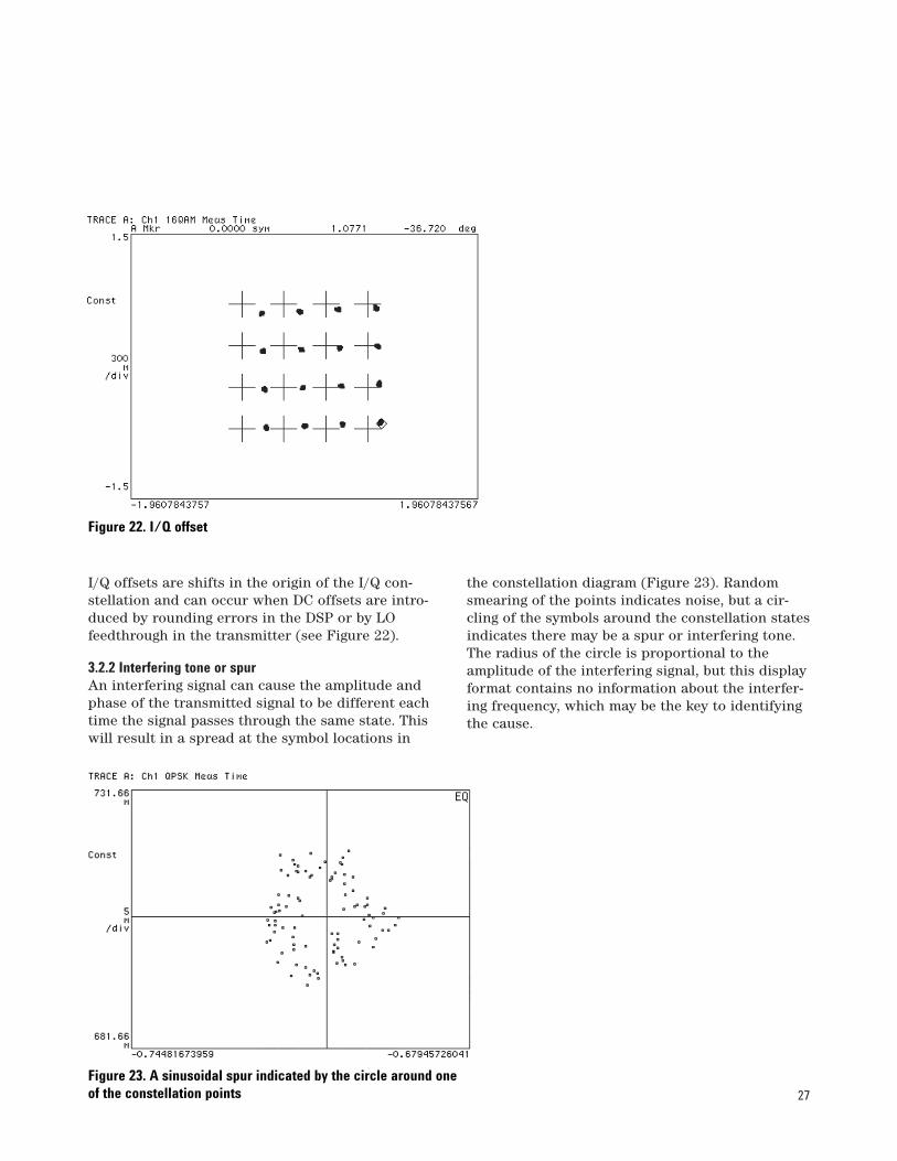
3.2.2 Interfering tone or spurAn interfering signal can cause the amplitude andphase of the transmitted signal to be different eachtime the signal passes through the same state. Thiswill result in a spread at the symbol locations in
the constellation diagram (Figure 23). Randomsmearing of the points indicates noise, but a cir-cling of the symbols around the constellation statesindicates there may be a spur or interfering tone.The radius of the circle is proportional to theamplitude of the interfering signal, but this displayformat contains no information about the interfer-ing frequency, which may be the key to identifyingthe cause.
Figure 22. I/Q offset
Figure 23. A sinusoidal spur indicated by the circle around oneof the constellation points

28
The presence of spurs on a modulated signal may bedifficult to determine on a constellation display orthrough spectrum analysis. An alternative parame-ter can be used to check signal quality: EVM. Adescription of EVM and how it relates to the BERcan be found in the Appendix. The magnitude of
the error vector versus time graph may hint thatthe error observed is sinusoidal in nature, butwhat is really needed is a method to determine the frequency of the spur.
Figure 24. Error vector spectrum reveals spur
Figure 25. Signal spectrum conceals spur

29
The error vector spectrum can indicate the fre-quency of spurious signals that cannot be observedon traditional spectrum analyzers or on a constel-lation display. In Figure 24, a spur offset from thecarrier by approximately 47 kHz is detected at theoutput of the IF filter. This spur was most likelycaused by an in-band CW signal undetectable bytraditional spectrum analysis (see Figure 25). Thisin-band CW interferer could be a harmonic of theprocessor clock, an intermodulation product, or an internally generated spur. This interfering tonecould cause the receiver to fail many of the per-formance verification tests.
3.2.3 Incorrect symbol rate The symbol clock of a digital radio dictates thesampling rate of the baseband I and Q waveformsrequired to accurately interpret the symbols andrecover the digital data at the receiver. In thetransmitter, the symbol rate dictates the creationof the baseband I and Q waveforms to properly putthe valid states in the correct locations, ensuringproper encoding of the digital data. It is imperativethat the transmitter and receiver have the samesymbol rate to be compatible.
An internal clock generator determines the symbol rate of a system. This generator must be set correctly. Symbol rate errors often occurwhen the wrong crystal frequency is used (forexample, if two numbers have been accidentallyswitched in the frequency specification). If noproblem exists with the crystal, the receiver is having a synchronization problem. Either thereceiver is not properly recovering the carrier fre-quency, or the receiver is not achieving symbollock. To recover the proper carrier frequency, the receiver must lock onto the phase of the carrier. To accurately extract the symbols from the carrier, the receiver must also determine when symbol transitions occur. A timing recoveryloop provides the mechanism for the receiver to achieve the necessary symbol lock. When thereceiver does not achieve proper phase lock and/or proper symbol lock, symbol rate errors occur. If you suspect an incorrect symbol rate and noproblem exists with the crystal, verify proper operation of the carrier and timing recovery circuitry of the receiver.
3.2.4 Baseband filtering problems Baseband filtering must be correctly implementedto provide the desired baseband frequency responseand to avoid ISI as well as overshoot of the base-band signal in time. The alpha parameter in araised-cosine filter defines the shape of the filterin the frequency domain. A low alpha creates asharp filter shape in the frequency domain, butalso creates high overshoot in the time domain,which can be recognized on a vector diagram. It is important to verify that the receiver has theappropriate baseband frequency response and time characteristics for the specified alpha.
In cases where baseband filtering is shared betweenthe transmitter and the receiver, the filters must becompatible and correctly implemented in each. Thetype of filter and the corresponding roll-off factor(alpha) are the key parameters that must be con-sidered. For raised-cosine filters, an error in theselection of alpha may result in undesirable ampli-tude overshoot in the signal. It may also result inISI. Incorrect filtering due to a wrong roll-off factormay affect the amount of interference from anadjacent channel signal. This could cause an other-wise good receiver to fail many of the performanceverification tests.
To verify baseband filter performance, examine the vector constellation diagram for excessive overshoot of the signal trajectory between symbolstates. The magnitude of the error vector versustime would be a good indicator of roll-off factordiscrepancies. If the wrong roll-off factor is used,the magnitude of the error vector will be highbetween symbol points and low at the symbolpoints (see Figure 26).

30
The correct roll-off factor can be found by usingdifferent roll-off factors in the VSA while viewingthe error vector time display. When the correctvalue is used, the magnitude of the error vectorbetween symbol decision points will be approxi-
mately equal to the magnitude of the error vectorat the decision points (Figure 27). Furthermore,equalization can be applied to decrease the errorscaused by baseband filtering problems.
Figure 27. Vector diagram and magnitude of the error vector versustime for correct roll-off factor
Figure 26. Vector diagram and magnitude of the error vector versustime for wrong roll-off factor

31
3.2.5 IF filter tilt or rippleThe IF filter attenuates out-of-channel interfer-ence. Errors in the design of this filter can affectthe overall signal. IF filter problems include filtertilt or ripple in the frequency response and varia-tions in group delay. Ideally, the filter should beflat across the frequency band of interest, and itsgroup delay should be constant across the samefrequency band. Filter tilt or ripple in the frequencyresponse causes linear distortion in the signal.Improper matching of any component between theantenna and the IF filter also causes tilt or ripple.For example, mismatch between the preselectingfilter and the LNA causes reflections that result in distortion of the overall frequency response ofthe receiver.
Filter tilt or ripple causes distortion on the demodu-lated baseband signal. This distortion is discerniblein the constellation diagram. Also, the magnitudeof the error vector will be higher than expected atthe symbol points as well as during symbol transi-tions. Since the IF filter is the main contributor to the frequency response of the receiver, IF filtershape distortion is observed and analyzed by per-forming a frequency response measurement on thefilter alone, as shown in Figure 28.
1:–10.172 dB 190.050 000 MHzCH1 S21 LOG 1 dB/REF–7 dB
PRm
Cor 1
Center 190.000 000 MHz Span 10.000 000 MHz
Figure 28. Undesired tilt and ripple in the IF filter

32
3.3 Table of impairments versus parametersaffectedTable 2 shows the physical impairments encoun-tered with digitally demodulated signals, and theparameters that these impairments affect.
Table 2. Impairments versus parameters affected
The key to troubleshooting is to identify the impair-ments that could be causing signal degradation.Each of the different impairments uniquely affectsthe quality of a digitally demodulated signal. Asthe table indicates, the I/Q constellation is typicallyaffected by physical impairments. Although theconstellation diagram is a good indicator of prob-lems, further analysis may be necessary to isolatethe source of the error. EVM is a powerful signalanalysis tool that can be scrutinized to pinpointsources of interference in receiver tests. Frequencyresponse and group delay measurements prove effec-tive in the detection of filtering problems. Phaseerror analysis can detect sources of unwantedphase noise.
Strategic use of these analysis tools will enhanceyour ability to track down sources of error in yourdigital radio receiver designs. The ability to quicklylocate design problems can greatly reduce productdevelopment and test verification times, and facili-tate the type approval of receiver designs.
Physical Impairments Parameters Affected
I/Q Gain Imbalance I/Q Constellation (Figure 20)
I/Q Quadrature Errors I/Q Constellation (Figure 21), Average EVM, Magnitude of the Error Vector versus
Time, Error Vector Spectrum
I/Q Offsets I/Q Constellation (Figure 22)
Interfering Tone or Spur I/Q Constellation (Figure 23), Average EVM, Error Vector Spectrum (Figure 24)
Incorrect Symbol Rate I/Q Constellation, Phase Error
Baseband Filtering Problems I/Q Constellation, Average EVM, Magnitude of the Error Vector versus Time (Figures 26 and 27)
IF Filter Tilt or Ripple I/Q Constellation, Magnitude of the Error Vector versus Time, Frequency Response (Figure 28), Group Delay

33
Digital RF communications receivers are challeng-ing to design, test, and troubleshoot. Two digitalradio receiver designs were discussed in this appli-cation note: I/Q demodulator and sampled IF.Receivers must meet strict conformance standards.Common in-channel and out-of-channel tests verifythat receiver designs meet these standards. Toreduce measurement errors, best practices should
be followed, with an awareness of measurementcaveats. A basic troubleshooting procedure helps to isolate design problems. Application of thesetesting and troubleshooting techniques can reduceproduct cycle times and increase confidence inproper operation after the receiver is manufac-tured and put into use.
4. Summary

34
BER is the best measurement to verify receiverperformance, but BER testing is not always possi-ble in the subsystems of a digital radio receiver.Also, BER can indicate a problem exists, but it maynot help identify the source of the problem. Analternative to BER testing is to examine the qualityof a demodulated signal. The most widely usedmodulation quality metric in digital RF communi-cations systems is the EVM. EVM provides a way to quantify the errors in digital demodulation andis sensitive to any signal impairment that affectsthe magnitude and phase trajectory of a demodu-lated signal.
As shown in Figure 29, the error vector is the vector difference between the reference signal and the measured signal. The error vector is acomplex quantity that contains a magnitude andphase component. Expressed another way, theerror vector is the residual noise and distortionremaining after an ideal version of the signal has
been stripped away. EVM is the root-mean-square(rms) value of the error vector over time at theinstants of the symbol clock transitions. By con-vention, EVM is usually normalized to the outer-most symbol magnitude at the symbol times andexpressed as a percentage:
EVM = (rms error vector / outermost symbol magnitude) x 100%
The error vector information of the trajectorybetween the points (viewable in the magnitude of the error vector versus time display of theAgilent 89441A VSA) helps you troubleshoot base-band filtering problems in your receiver design(see section 3.2.4). Also, the spectrum of the errorvector can help you locate sources of interference(see section 3.2.2). The magnitude error and phaseerror between the two vectors provide a way toview unwanted phase and amplitude modulationthat may occur in your receiver.
5. Appendix: From Bit Error Rate (BER) to Error Vector Magnitude (EVM)
Q
I
Magnitude Error
Phase of Error Vector
Measured Signal
Ideal Signal(Reference)
Phase Error
Error Vector
Magnitude of Error Vector
θ
φ
Figure 29. EVM and related quantities

35
EVM may also be normalized to the square root of the average symbol power. In this way, EVM can be related to the SNR:
SNR = –20 * log (EVM / 100%)
The importance of the above equation is that itrelates EVM to BER through the SNR.
Many textbooks have standard curves that relateBER to SNR, as in Figure 30 (see [9]). Generally,these curves assume that the noise is AdditiveWhite Gaussian Noise (AWGN) with a finite peak-to-average ratio, or crest factor. The assumptionsmade in generating textbook plots of BER versusSNR will not necessarily apply to a particularreceiver. The noise in a receiver under test, for
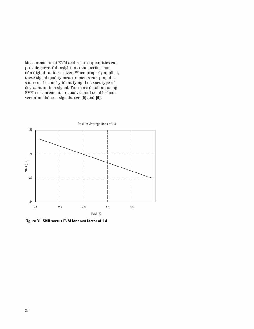
example, may not be AWGN but may instead have a strong spectral component. In addition, the steep slope of BER curves makes BER estima-tions from measured SNR (or EVM) more prone toerror. However, EVM provides an easily measuredfigure-of-merit that can be used to monitor designchanges, locate design problems and, when base-lined against a BER measurement, indicate thelikelihood that a design will meet the requiredspecifications. Hence, the connection of BER toEVM is through the SNR, the more general indica-tor of likely signal quality (see Figure 31).
Figure 30. Probability of error versus SNR
16-PSK
16-APK or 16 QAM
8-PSK8-APK
BPSK
4-PSK(QAM)
Class IQPR
10–10
10–9
10–8
10–7
10–6
10–5
10–4
10–3
6 8 10 12 14 16 18 20 22 24 26
SNR (dB)
P(e)
36
Measurements of EVM and related quantities canprovide powerful insight into the performance of a digital radio receiver. When properly applied,these signal quality measurements can pinpointsources of error by identifying the exact type ofdegradation in a signal. For more detail on usingEVM measurements to analyze and troubleshootvector-modulated signals, see [5] and [6].
Peak-to-Average Ratio of 1.4
2.5 2.7 2.9 3.1 3.3
30
28
26
24
EVM (%)
SNR
(dB)
Figure 31. SNR versus EVM for crest factor of 1.4
37
a Alpha (roll-off factor) of a Nyquist filterACP Adjacent Channel PowerADC Analog-to-Digital ConverterAGC Automatic Gain ControlALC Automatic Level ControlASIC Application-Specific Integrated CircuitAWGN Additive White Gaussian NoiseBER Bit Error RateBERT Bit Error Rate TesterBT Bandwidth-Time product (roll-off factor)
of a Gaussian filterCDMA Code Division Multiple AccessCW Continuous WaveDDC Digital Down ConverterDSP Digital Signal Processor DUT Device Under TestETSI European Telecommunications Standard
InstituteEVM Error Vector MagnitudeFER Frame Erasure RateFFT Fast Fourier TransformGSM Global System for Mobile communicationsI In-phaseIC Integrated CircuitIF Intermediate FrequencyISI Inter-Symbol InterferenceITU International Telecommunications Union
LNA Low-Noise AmplifierLO Local OscillatorNADC North American Digital CellularPDC Pacific Digital CellularPHS Personal Handyphone SystemPRBS Pseudo-Random Binary SequenceQ Quadrature-phaseRBER Residual Bit Error RateRF Radio FrequencySMR Specialized Mobile RadioSAW Surface Acoustic WaveSNR Signal-to-Noise RatioTDMA Time Division Multiple AccessTIA Telecommunications Industry AssociationTOI Third-Order InterceptUUT Unit Under TestVNA Vector Network AnalyzerVSA Vector Signal Analyzer
6. Symbols and Acronyms

38
[1] Testing and Troubleshooting Digital RFCommunications Transmitter Designs,Agilent Application Note 1313, literaturenumber 5968-3578E.
[2] Digital Modulation in CommunicationsSystems—An Introduction, AgilentApplication Note 1298, literature number5965-7160E.
[3] Vector Modulation Measurements, AgilentApplication Note 343-4, literature number5952-3703.
[4] Measuring Bit Error Rate using the AgilentESG-D Series RF Signal Generators OptionUN7, literature number 5966-4098E.
[5] Using Vector Modulation Analysis in the
Integration, Troubleshooting, and Design
of Digital RF Communications Systems,
Agilent Product Note 89400-8, literature number 5091-8687E.
[6] Ten Steps to a Perfect Digital DemodulationMeasurement, Agilent Product Note 89400-14A,literature number 5966-0444E.
[7] Fundamentals of RF and Microwave NoiseFigure Measurements, Agilent ApplicationNote 57-1, literature number 5952-8255.
[8] Measuring Third-Order Intermodulation, N dB Bandwidth, and Percent AM with Built-in Functions, Agilent Product Note 8590-8,literature number 5091-4052E.
[9] K. Feher, Digital Communications, PrenticeHall 1981: Englewood Cliffs, New Jersey.
[10] Theodore S. Rappaport, Wireless Communica-tions: Principles and Practices, Prentice Hall1996: Upper Saddle River, New Jersey.
[11] Bernard Sklar, Rayleigh Fading Channels inMobile Digital Communication Systems Part I:Characterization, IEEE CommunicationsMagazine, July 1997, Vol. 35 No. 7.
[12] Robert H. Walden, Performance Trends for Analog-to-Digital Converters, IEEECommunications Magazine, February 1999,Vol. 37 No. 2.
7. References
By internet, phone, or fax, get assistancewith all your test and measurement needs.
Online Assistancewww.agilent.com/find/assistPhone or FaxUnited States:(tel) 1 800 452 4844
Canada:(tel) 1 877 894 4414(fax) (905) 206 4120
Europe:(tel) (31 20) 547 2323(fax) (31 20) 547 2390
Japan:(tel) (81) 426 56 7832(fax) (81) 426 56 7840
Latin America:(tel) (305) 269 7500(fax) (305) 269 7599
Australia:(tel) 1 800 629 485 (fax) (61 3) 9272 0749
New Zealand:(tel) 0 800 738 378 (fax) (64 4) 495 8950
Asia Pacific:(tel) (852) 3197 7777(fax) (852) 2506 9284
Product specifications and descriptions in this document subject to change without notice.
Copyright © 1999, 2000 Agilent TechnologiesPrinted in U.S.A. 5/005968-3579E