Embed Size (px)
Citation preview

Creation Date: 07/23/09 Page 1 of 21 Modification Date: 05/20/10
Aeroflex Colorado Springs Application Note AN-LVDS-002-003
Theory of Operation and VDD Fault Scenario for LVDS Products
Table 1: Cross Reference of Applicable Products
Product Name: Manufacturer Part
Number SMD # Device
Type Internal PIC*
3.3-VOLT QUAD DRIVER UT54LVDS031LV/E 5962-98651 02, 03, 04, 05
WD03, WD07, WD28, WD30
3.3-VOLT QUAD RECEIVER UT54LVDS032LV/E 5962-98652 02, 03, 04, 05
WD04, WD08, WD29, WD31
3.3V QUAD RECEIVER with Integrated Termination Resistor
UT54LVDS032LVT 5962-04201 01, 02 WD06, WD10
SpaceWire Physical Layer Transceiver
UT200SpWPHY01 5962-06232 01, 02 WD37
4-Port SpaceWire Router UT200SpW4RTR 5962-08244 01, 02 WD41 *PIC = Product Identification Code
1.0 Overview
Recently there have been a number of papers published falsely suggesting that Low Voltage Differential Signaling drivers do not contain current sources, and that there exists a realistic probability of catastrophic fault conditions occurring on LVDS devices[1]. This application note will describe Aeroflex LVDS driver and receiver operation, and present results of lab testing performed to evaluate the hypothetical failure mode of a LVDS driver/receiver due to a severe power supply fault. The SpaceWire Standard ECSS-E-ST-50-12C [2] calls for a Low Voltage Differential Signaling (LVDS) physical layer as defined in ANSI/TIA/EIA-644 [3], Electrical Characteristics of Low Voltage Differential Signaling Interface Circuits. Aeroflex LVDS drivers are compliant to the ANSI/TIA/EIA-644 standard and contain a current source that generates the required voltage across a 100Ω, parallel, resistor. A hypothetical failure mode where the supply voltage, VDD, exceeds the ABSOLUTE MAXIMUM RATINGS defined in the Aeroflex Datasheet and corresponding DSCC SMD was examined. The laboratory testing results are reported in this application note. 2.0 Technical Background
Low Voltage Differential Signaling is useful in applications that require low power, low noise, and high-speed point-to-point communications. The SpaceWire physical layer uses Data-Strobe (DS) Encoded LVDS to communicate serial, full-duplex, bidirectional data. Figure 1 shows a notional SpaceWire Link using the LVDS physical layer, the operation of LVDS will be explained later in this paper.

Creation Date: 07/23/09 Page 2 of 21 Modification Date: 05/20/10
Figure 1. Single point to point SpaceWire Link The Input/Output signal levels are defined by ANSI/TIA/EIA-644, which is an electrical signaling standard only; it does not define a protocol. Instead, the protocol is defined in the SpaceWire Standard specification ECSS-S-ST-50-12C, which is derived from IEEE 1355-1995. 2.1 LVDS Functionality LVDS is a method used to transmit and receive hundreds of megabits per second over differential media using a low voltage signal swing (~350mV). LVDS communications are preformed by a driver and a receiver. The driver accepts a standard Complementary Metal Oxide Semiconductor (CMOS) signal and outputs a constant current, differential, signal. The LVDS receiver senses the differential voltage across a 100Ω termination resistor and outputs a standard CMOS signal. Standard CMOS signals have voltage levels of 0.0V for a logic Low and 3.3V or 5.0V for logic High. The LVDS driver contains a constant current source that outputs 3.5mA. The driver output current travels through a 100Ω resistive load located across the receiver inputs. The current flow through the resistor results in a 350mV potential across the differential terminals. The direction of the driver’s constant current source will determine the logic state at the receiver. Figure 2 depicts a notional block diagram of a LVDS driver and receiver interface.
Creation Date: 07/23/09 Page 3 of 21 Modification Date: 05/20/10
Figure 2. Point-to-point LVDS Driver Receiver configuration
The differential aspect of LVDS allows systems to run at high data rates, with low switching power, high noise immunity, and common mode range. Single ended data transfer schemes, on the other hand, tend to be very sensitive to common mode differences because the voltage reference is relative to a local ground connection at the driver and receiver.
Data communications can occur across cables up to ten meters in length. Common mode problems become more pronounced as the end points become separated by further distances. Communications standards, like SpaceWire, which require reliable, high data rate, communications over distances of up to 10 meters must be insensitive to noise and common mode disparities. LVDS satisfies this requirement, single ended signaling does not. The LVDS driver works by using NMOS Field Effect Transistors (FETs) to control the direction of the constant 3.5mA current source through the termination resistor. The driver current, flowing through the 100Ω termination resistor placed across the differential inputs of the receiver, generates a +/-350mV I-R drop which is sensed as a logic high/low by the receiver. The LVDS receiver has very high DC input impedance, so the majority of the driver’s current flows, in a loop, from the source terminal through the 100Ω termination resistor and back into the sinking terminal. A quick calculation shows that the proper voltage is generated across the termination resistor. Recalling Ohms Law IRV = where V = Voltage, I = Current, and R = Resistance.
mVmAIRV 350100*5.3 =Ω== . This low voltage signal shows that another advantage of using LVDS is the resulting low power consumption. An example of LVDS power can be easily calculated using P=I*V where P = Power, V = Voltage, and I = Current. PowerLVDS=3.5mA * 350mV = 1.225mW at any frequency and loading. As compared to a single ended CMOS signal is very dependant upon loading capacitance and frequency; consuming significantly more switching power than LVDS as demonstrated in the following equation: PowerCMOS=C*V²*f = 10pF*3.0V*100MHz = 9mW. Figure 3 shows the notional LVDS driver configuration. Two pairs of NMOS transistors that are used to steer the constant current signal to drive either a logic low or high across the receiver terminals. The driver differential outputs are tapped off of the middle of each leg of the stacked NMOSFETs.

Creation Date: 07/23/09 Page 4 of 21 Modification Date: 05/20/10
Figure 3. Notional LVDS Driver Configuration
When the driver output current direction changes, the direction of current flow across the termination resistor will change accordingly, creating the logic 1 or 0 state at the receiver output. Current flow through NMOSFETs Q1 and Q4 creates a logic high state, and current flow through Q2 and Q3 creates a logic low state at the receiver. Figure 4 shows the current flow through the driver/receiver system during the logic low condition. The constant current source drives +3.5mA through Q2 and into the negative half of the LVDS bus. The current reaches the termination resistor located at the receiver, flows back through the positive half of the bus, returns to the terminal drain of Q3 in the driver, and then passes into the driver VSS plane. Because the current flowing through the termination resistor is from the negative to the positive receiver terminals, a forward voltage drop occurs and a logical low appears at the output (ROUT) of the receiver.
OFF
OFF
ON
ON
-
+100Ω
Constant Current Source 3.5mA
ROUT
+
+
Q1 Q2
Q3Q4
Figure 4. Logic Low (zero, 0) State

Creation Date: 07/23/09 Page 5 of 21 Modification Date: 05/20/10
By disabling Q2 and Q3 and enabling Q1 and Q4, the converse is true. The current changes direction by flowing out of the positive driver terminal, through the termination resistor, and returning to the driver at the negative terminal. The current flow from the positive to negative terminal through the 100Ω termination resistor creates a forward voltage drop in that direction that is sensed by the receiver as a logic high at the receiver output (ROUT)
Figure 5. Logic High (one, 1) State
The LVDS receiver will sense a 200mV separation between the differential signal terminals and output the corresponding CMOS logic level. The differential nature of the LVDS standard enables the receiver to ignore noise that is mutually coupled on the differential signaling pair. Common mode rejection is improved over CMOS/TTL signaling because of the small voltage swing and the 1.2V nominal output voltage offset generated by the driver. A typical high level output voltage for the driver is around 200mV while the low level output is -200mV, centered on the offset voltage.
Creation Date: 07/23/09 Page 6 of 21 Modification Date: 05/20/10
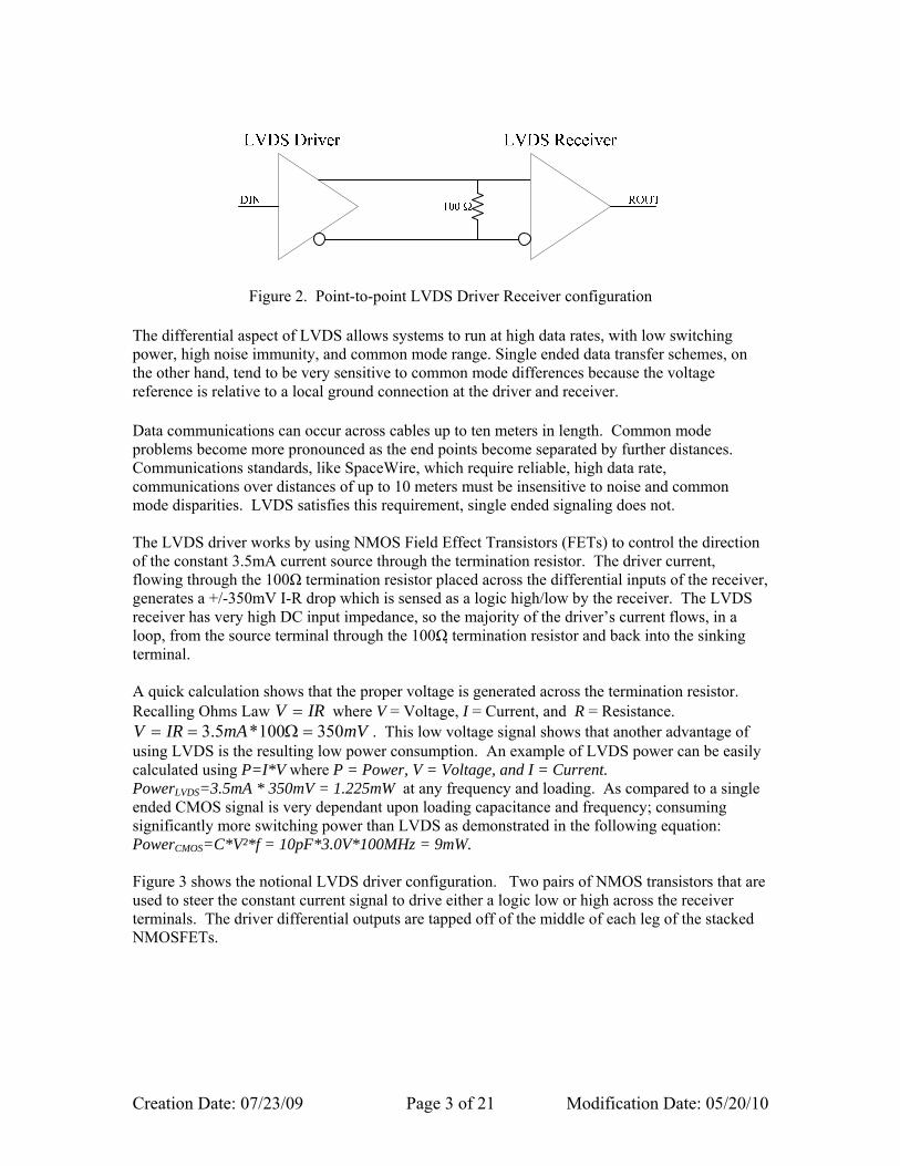
3.0 LVDS Laboratory Experiment of Power Supply Faults The UT54LVDS031LV and UT54LVDS032LV devices were used for the laboratory experiment. To demonstrate the devices response to an over voltage failure mode, these experiments were performed with an 8.0V ramp on power supplies and I/O while monitoring the driver inputs (DIN), driver outputs (DOUT+/-), receiver inputs (RIN+/- across 100Ω termination resistor), and receiver output (ROUT). The following sections show set up conditions, data, and results for each experiment. All data was taken at 25°C (ambient) with a 1 minute (Tests 1-5) or a 15 second (Tests 6 – 9) dwell time at each voltage point.
100 Ω
UT54LVDS031LV UT54LVDS032LV
ROUTDIN
VDD(Driver) VDD(Receiver)
DOUT+
DOUT-
RIN+
RIN-
VSS(Receiver)VSS(Driver)
Figure 6. Standard LVDS driver/receiver test configuration

Creation Date: 07/23/09 Page 7 of 21 Modification Date: 05/20/10
3.1 Laboratory Test 1 The first experiment conducted in the lab at ambient conditions used the following test setup.
100 Ω
LVDS Driver
DIN
VDD(Driver)
DOUT+
DOUT-
1 2
3
10MHz 0 to 3.3V swing
Test 1 configuration
DIN = 10MHz with a 0 to 3.3V swing, EN = 3.3V, /EN = 0V The first test demonstrates the differential output voltage response (DOUT+ and DOUT-) signals to a driver VDD fault. The driver’s power supply was ramped from 3.3V to 10V. A standard lab power supply with 2.5A current limit was used for this experiment. The power supply current limiting capabilities prevented VDD on the UT54LVDS031LV driver from ramping past 7.0V when the device under test (DUT) witnessed catastrophic failure due to VDD stress. The results of the tests are shown in Table 2.
VDD(Driver) (V)
I VDD(Driver)
(mA)
DOUT+/RIN+ (V)
Average
DOUT-/RIN- (V)
Average Point 1 Point 1 Point 2 Point 3
3.3 12.18 1.28 1.4 3.6 12.67 1.31 1.424 4 13.21 1.33 1.44 5 15.16 1.43 1.526 6 22.67 1.81 1.88 7 255 2.49 2.6
Table 2. Test 1 Results
Table 2 shows that with 7V on the driver power supply, the differential outputs of the device did not exceed 2.6V. Due to the high voltage on the driver VDD, the device failed to function after the over voltage. These results indicate that a VDD fault on the driver did not propagate a high voltage to the receiver.

Creation Date: 07/23/09 Page 8 of 21 Modification Date: 05/20/10
3.2 Laboratory Test 2
The second experiment conducted in the lab at ambient conditions used the following test setup.
100 Ω
LVDS Driver LVDS Receiver
ROUTDIN
VDD(Driver) VDD(Receiver)
DOUT+
DOUT-
RIN+
RIN-
12
3
4
5
10MHz 0 to 3.3V swing
Test 2 configuration DIN = 10MHz with a 0 to 3.3V swing, EN = 3.3V, /EN = 0V
The second test evaluated how a standard LVDS driver/receiver configuration responds to a driver power supply over voltage fault. The voltage and current of the driver and receiver power supplies was monitored. The differential output voltages on the DOUT+/RIN+ and DOUT-/RIN- signals across the 100Ω termination resistor and the output of the receiver (ROUT). VDD(Driver) was ramped from a nominal 3.3V to 10V. A standard lab power supply with 2.5A current limit was used for this experiment. The power supply current limiting capabilities prevented VDD on the UT54LVDS031LV driver from ramping past 8.0V. The test results are shown in Table 3.
VDD(Driver) (V)
I VDD(Driver)
(mA)
DOUT+/RIN+(V)
Average
DOUT-/RIN-(V)
Average
ROUT (V)
Amplitude VDD(Receiver)
(V)
I VDD(Receiver)
(mA) Point 1 Point 1 Point 2 Point 3 Point 5 Point 4 Point 4
3.3 12.49 1.301 1.409 3.12 3.3 6.66 3.6 13.17 1.33 1.44 3.04 3.3 6.63 4 13.73 1.35 1.46 3.2 3.3 6.62 5 15.95 1.47 1.56 3.04 3.3 6.56 6 23.31 1.833 1.92 3.2 3.3 6.54 7 261 2.51 2.61 3.12 3.3 6.07 8 500 2.38 3.2 3.42 3.3 10.5
Table 3. Test 2 Results
Table 3 indicates that the standard LVDS driver/receiver configuration did not propagate a high voltage fault when VDD on the driver is ramped to 8.0V. The maximum voltage seen on the DOUT+/RIN+ and DOUT-/RIN- signals are within the absolute maximum ratings for both devices. The high voltage stress on the driver VDD permanently damaged the driver device without propagating the fault to the receiver. The UT54LVDS032LV receiver continued to function after the fault condition.
Creation Date: 07/23/09 Page 9 of 21 Modification Date: 05/20/10
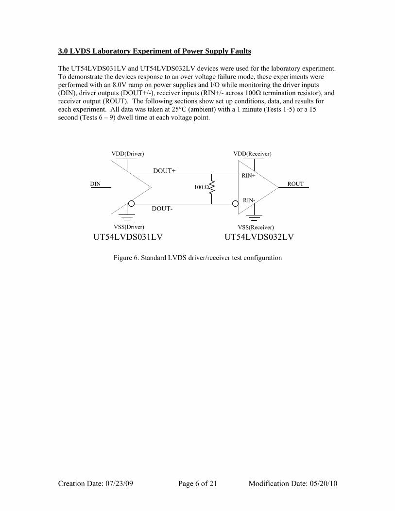
3.3 Laboratory Test 3 The third experiment conducted in the lab at ambient conditions used the following test setup.
LVDS Driver
DIN
VDD(Driver)
DOUT+
DOUT-
1
2 Test 3 configuration
DIN = VSS, EN = 3.3V, /EN = 0V
The third test evaluated the output short circuit capabilities of the UT54LVDS031LV driver when VDD on the driver is ramped from nominal 3.3V to 10V. The voltage and current of the driver power supply, and the short circuit output (IOS) current on the DOUT- differential output were monitored. A standard lab power supply with 2.5A current limit was used for this experiment. The power supplies current limiting capabilities prevented VDD of the UT54LVDS031LV driver from being ramped past 8.0V. The results of the tests are shown in Table 4.
VDD(Driver)(V)
I VDD(Driver)(mA)
IOS (mA)
Point 1 Point 1 Point 2 3.3 11.81 3.22 3.6 12.28 3.35 4 12.69 3.46
4.5 13.38 3.66 5 14.62 4.08
5.5 16.64 4.81 6 19.85 5.96 7 36.01 11.9
7.5 53.42 17.42 8 91.11 20.6
Table 4. Test 3 Results
Table 4 shows that the maximum short circuit output current with VDD(Driver) equal to 8V is ~20.6mA. This is important because it means that if the VDD(Driver) could propagate a high voltage on the LVDS bus, the current is too weak to over drive a power supply on the receiver.

Creation Date: 07/23/09 Page 10 of 21 Modification Date: 05/20/10
3.4 Laboratory Test 4 The fourth experiment conducted in the lab at ambient conditions used the following test setup.
Test 4 configuration RIN+/- = 10MHz 1.2V+/- 100mV, EN = 3.3V, /EN = 0V
The fourth test evaluated the receiver output (ROUT) performance when VDD on the receiver is ramped from nominal 3.3V to 10V. The voltage and current of the receiver power supply and the receiver output (ROUT) were monitored. The LVDS input signals at RIN+/- inputs were driven at nominal LVDS levels. A standard lab power supply with 2.5A current limit was used for this experiment. The power supplies current limiting capabilities prevented VDD of the UT54LVDS032LV receiver from being ramped past 8.0V. The results of the tests are shown in Table 5.
VDD(Receiver) (V)
I VDD(Receiver)
(mA)
RIN+ (V)
Average
RIN- (V)
Average
ROUT (V)
Amplitude Point 1 Point 1 Point 2 Point 3 Point 4
3.3 6.69 1.28 1.14 3.12 3.6 7.09 1.28 1.408 3.44 4 7.74 1.28 1.39 4 5 10.82 1.29 1.41 4.88 6 24.45 1.29 1.42 5.76 7 50.7 1.29 1.42 6.48 8 110 1.29 1.42 6.96
Table 5. Test 4 Results
Table 5 shows that the receiver output voltage reflects the voltage level on VDD of the receiver. A high voltage on the receiver power supply will allow a high voltage signal to propagate to the output of the receiver because these outputs are CMOS buffers instead of Low Voltage Differential Signaling.
Creation Date: 07/23/09 Page 11 of 21 Modification Date: 05/20/10
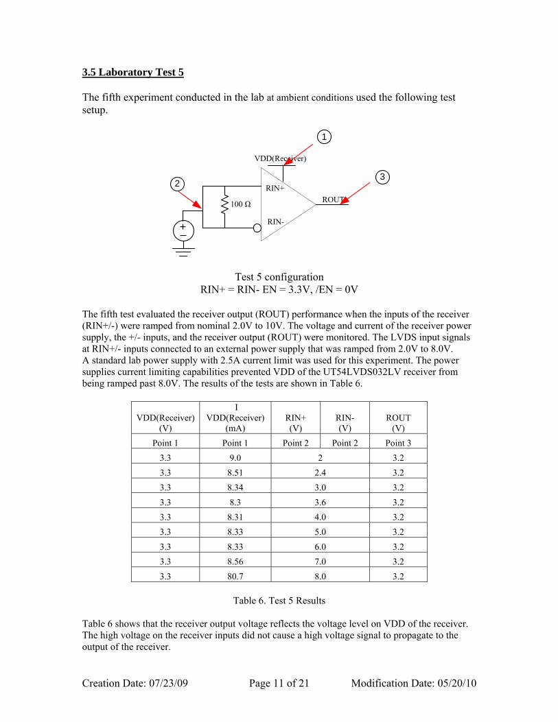
3.5 Laboratory Test 5 The fifth experiment conducted in the lab at ambient conditions used the following test setup.
100 Ω ROUT
VDD(Receiver)
RIN+
RIN-
2
1
3
+
Test 5 configuration RIN+ = RIN- EN = 3.3V, /EN = 0V
The fifth test evaluated the receiver output (ROUT) performance when the inputs of the receiver (RIN+/-) were ramped from nominal 2.0V to 10V. The voltage and current of the receiver power supply, the +/- inputs, and the receiver output (ROUT) were monitored. The LVDS input signals at RIN+/- inputs connected to an external power supply that was ramped from 2.0V to 8.0V. A standard lab power supply with 2.5A current limit was used for this experiment. The power supplies current limiting capabilities prevented VDD of the UT54LVDS032LV receiver from being ramped past 8.0V. The results of the tests are shown in Table 6.
VDD(Receiver) (V)
I VDD(Receiver)
(mA) RIN+ (V)
RIN- (V)
ROUT (V)
Point 1 Point 1 Point 2 Point 2 Point 3 3.3 9.0 2 3.2 3.3 8.51 2.4 3.2 3.3 8.34 3.0 3.2 3.3 8.3 3.6 3.2 3.3 8.31 4.0 3.2 3.3 8.33 5.0 3.2 3.3 8.33 6.0 3.2 3.3 8.56 7.0 3.2 3.3 80.7 8.0 3.2
Table 6. Test 5 Results
Table 6 shows that the receiver output voltage reflects the voltage level on VDD of the receiver. The high voltage on the receiver inputs did not cause a high voltage signal to propagate to the output of the receiver.

Creation Date: 07/23/09 Page 12 of 21 Modification Date: 05/20/10
3.6 Laboratory Test 6 The sixth experiment conducted in the lab at ambient conditions used the following test setup.
100 Ω ROUT1DIN1
100 ΩDIN2 ROUT2
100 Ω ROUT3DIN3
100 ΩDIN4 ROUT4
LVDS Driver LVDS Receiver
VDD(Driver)=0.0V VDD(Receiver)
3 4
1
2
VSS(Driver) VSS(Receiver)
Test 6 configuration
EN = /EN = 0.0V The sixth test evaluated the differential lines (DOUT+/RIN+ and DOUT-/RIN-) with the receiver powered and the driver unpowered (cold spare mode). The inputs of the driver (DIN) were set to 0.0V and the supply voltage of the receiver, VDD(Receiver), was ramped to 8.0V. The voltage and current of the receiver and driver power supplies and the +/- differential signals were monitored. A standard lab power supply with 2.5A current limit was used for this experiment. Three new pairs of UT54LVDS031LV and UT54LVDS032LV parts were separately tested. The average results from the 3 test runs are shown below in Table 7. There were no significant differences between the 3 test runs. Table 7 shows a different voltage sequence for the ramping of VDD(Receiver), compared to the linear step ramp that was used in tests 1 – 5. Each voltage step was held for 15 seconds before moving to the next step, providing more than enough time for any overheating damage to present.
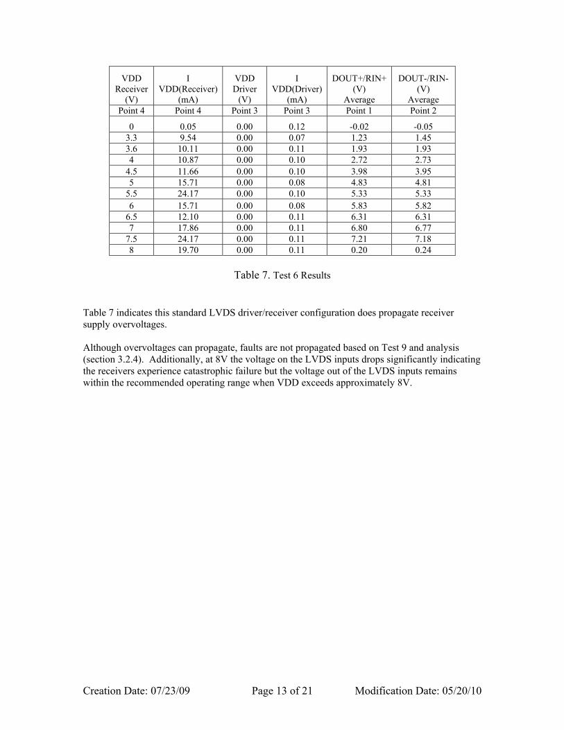
Creation Date: 07/23/09 Page 13 of 21 Modification Date: 05/20/10
VDD Receiver
(V)
I VDD(Receiver)
(mA)
VDD Driver
(V)
I VDD(Driver)
(mA)
DOUT+/RIN+(V)
Average
DOUT-/RIN- (V)
Average Point 4 Point 4 Point 3 Point 3 Point 1 Point 2
0 0.05 0.00 0.12 -0.02 -0.05 3.3 9.54 0.00 0.07 1.23 1.45 3.6 10.11 0.00 0.11 1.93 1.93 4 10.87 0.00 0.10 2.72 2.73
4.5 11.66 0.00 0.10 3.98 3.95 5 15.71 0.00 0.08 4.83 4.81
5.5 24.17 0.00 0.10 5.33 5.33 6 15.71 0.00 0.08 5.83 5.82
6.5 12.10 0.00 0.11 6.31 6.31 7 17.86 0.00 0.11 6.80 6.77
7.5 24.17 0.00 0.11 7.21 7.18 8 19.70 0.00 0.11 0.20 0.24
Table 7. Test 6 Results
Table 7 indicates this standard LVDS driver/receiver configuration does propagate receiver supply overvoltages. Although overvoltages can propagate, faults are not propagated based on Test 9 and analysis (section 3.2.4). Additionally, at 8V the voltage on the LVDS inputs drops significantly indicating the receivers experience catastrophic failure but the voltage out of the LVDS inputs remains within the recommended operating range when VDD exceeds approximately 8V.

Creation Date: 07/23/09 Page 14 of 21 Modification Date: 05/20/10
3.7 Laboratory Test 7 The seventh experiment conducted in the lab at ambient conditions used the following test setup.
Test 7 configuration
Driver: EN = 0.0V /EN = 3.3V Receiver: EN = /EN = 0.0V
The seventh test evaluated the differential lines (DOUT+/RIN+ and DOUT-/RIN-) with the receiver powered and the driver in a tristated configuration. This was accomplished by setting the enable signals on the UT54LVDS031LV to EN=0.0V and /EN=3.3V. The inputs of the driver (DIN) were set to 0.0V, VDD(Driver) to 3.3V, and the supply voltage of the receiver, VDD(Receiver), was ramped to 8.0V. The voltage and current of the receiver and driver power supplies, the +/- differential signals, and the current out of the driver VSS(Driver) were monitored. A standard lab power supply with 2.5A current limit was used for this experiment. 3 new pairs of UT54LVDS031LV and UT54LVDS032LV parts were separately tested.
Creation Date: 07/23/09 Page 15 of 21 Modification Date: 05/20/10
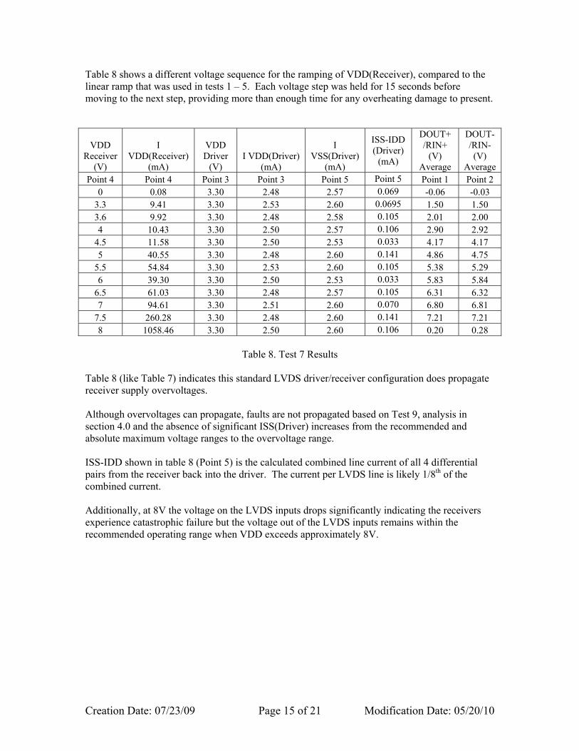
Table 8 shows a different voltage sequence for the ramping of VDD(Receiver), compared to the linear ramp that was used in tests 1 – 5. Each voltage step was held for 15 seconds before moving to the next step, providing more than enough time for any overheating damage to present.
VDD Receiver
(V)
I VDD(Receiver)
(mA)
VDD Driver
(V) I VDD(Driver)
(mA)
I VSS(Driver)
(mA)
ISS-IDD (Driver)
(mA)
DOUT+ /RIN+
(V) Average
DOUT-/RIN- (V)
Average Point 4 Point 4 Point 3 Point 3 Point 5 Point 5 Point 1 Point 2
0 0.08 3.30 2.48 2.57 0.069 -0.06 -0.03 3.3 9.41 3.30 2.53 2.60 0.0695 1.50 1.50 3.6 9.92 3.30 2.48 2.58 0.105 2.01 2.00 4 10.43 3.30 2.50 2.57 0.106 2.90 2.92
4.5 11.58 3.30 2.50 2.53 0.033 4.17 4.17 5 40.55 3.30 2.48 2.60 0.141 4.86 4.75
5.5 54.84 3.30 2.53 2.60 0.105 5.38 5.29 6 39.30 3.30 2.50 2.53 0.033 5.83 5.84
6.5 61.03 3.30 2.48 2.57 0.105 6.31 6.32 7 94.61 3.30 2.51 2.60 0.070 6.80 6.81
7.5 260.28 3.30 2.48 2.60 0.141 7.21 7.21 8 1058.46 3.30 2.50 2.60 0.106 0.20 0.28
Table 8. Test 7 Results
Table 8 (like Table 7) indicates this standard LVDS driver/receiver configuration does propagate receiver supply overvoltages. Although overvoltages can propagate, faults are not propagated based on Test 9, analysis in section 4.0 and the absence of significant ISS(Driver) increases from the recommended and absolute maximum voltage ranges to the overvoltage range. ISS-IDD shown in table 8 (Point 5) is the calculated combined line current of all 4 differential pairs from the receiver back into the driver. The current per LVDS line is likely 1/8th of the combined current. Additionally, at 8V the voltage on the LVDS inputs drops significantly indicating the receivers experience catastrophic failure but the voltage out of the LVDS inputs remains within the recommended operating range when VDD exceeds approximately 8V.

Creation Date: 07/23/09 Page 16 of 21 Modification Date: 05/20/10
3.8 Laboratory Test 8 The eighth experiment expanded on Test 1 and was conducted in the lab at ambient conditions used the following test setup.
Test 8 configuration EN = 3.3V, /EN = 0V DIN1 = VDD(Driver)
DIN2 = 10MHz with a 0 to 3.3V swing DIN3 = DIN4 = 0.0V
The eighth test evaluated the differential lines (DOUT+ and DOUT-) performance when VDD on the driver is ramped from 0.0V to 8.0V. This was accomplished by setting the enable signals on the UT54LVDS031LV to EN=3.3V and /EN=0.0V. Input #1 (DIN1) was set to VDD(Driver), input #2 (DIN2) was stimulated with a 10MHz square wave with 0.0 to 3.3V peak-to-peak, and inputs #3 and #4 were set to 0.0V. The voltage and current of the driver power supply, voltage across the termination resistor across DOUT1, voltage at DOUT1+, voltage at DOUT2+, and voltage at DOUT2- were monitored. A standard lab power supply with 2.5A current limit was used for this experiment. 3 new UT54LVDS031LV parts were separately tested.
Creation Date: 07/23/09 Page 17 of 21 Modification Date: 05/20/10
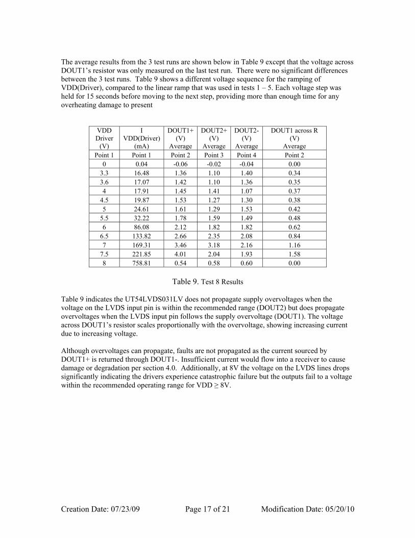
The average results from the 3 test runs are shown below in Table 9 except that the voltage across DOUT1’s resistor was only measured on the last test run. There were no significant differences between the 3 test runs. Table 9 shows a different voltage sequence for the ramping of VDD(Driver), compared to the linear ramp that was used in tests 1 – 5. Each voltage step was held for 15 seconds before moving to the next step, providing more than enough time for any overheating damage to present
VDD Driver
(V)
I VDD(Driver)
(mA)
DOUT1+(V)
Average
DOUT2+(V)
Average
DOUT2-(V)
Average
DOUT1 across R (V)
Average Point 1 Point 1 Point 2 Point 3 Point 4 Point 2
0 0.04 -0.06 -0.02 -0.04 0.00 3.3 16.48 1.36 1.10 1.40 0.34 3.6 17.07 1.42 1.10 1.36 0.35 4 17.91 1.45 1.41 1.07 0.37
4.5 19.87 1.53 1.27 1.30 0.38 5 24.61 1.61 1.29 1.53 0.42
5.5 32.22 1.78 1.59 1.49 0.48 6 86.08 2.12 1.82 1.82 0.62
6.5 133.82 2.66 2.35 2.08 0.84 7 169.31 3.46 3.18 2.16 1.16
7.5 221.85 4.01 2.04 1.93 1.58 8 758.81 0.54 0.58 0.60 0.00
Table 9. Test 8 Results
Table 9 indicates the UT54LVDS031LV does not propagate supply overvoltages when the voltage on the LVDS input pin is within the recommended range (DOUT2) but does propagate overvoltages when the LVDS input pin follows the supply overvoltage (DOUT1). The voltage across DOUT1’s resistor scales proportionally with the overvoltage, showing increasing current due to increasing voltage. Although overvoltages can propagate, faults are not propagated as the current sourced by DOUT1+ is returned through DOUT1-. Insufficient current would flow into a receiver to cause damage or degradation per section 4.0. Additionally, at 8V the voltage on the LVDS lines drops significantly indicating the drivers experience catastrophic failure but the outputs fail to a voltage within the recommended operating range for VDD ≥ 8V.
Creation Date: 07/23/09 Page 18 of 21 Modification Date: 05/20/10
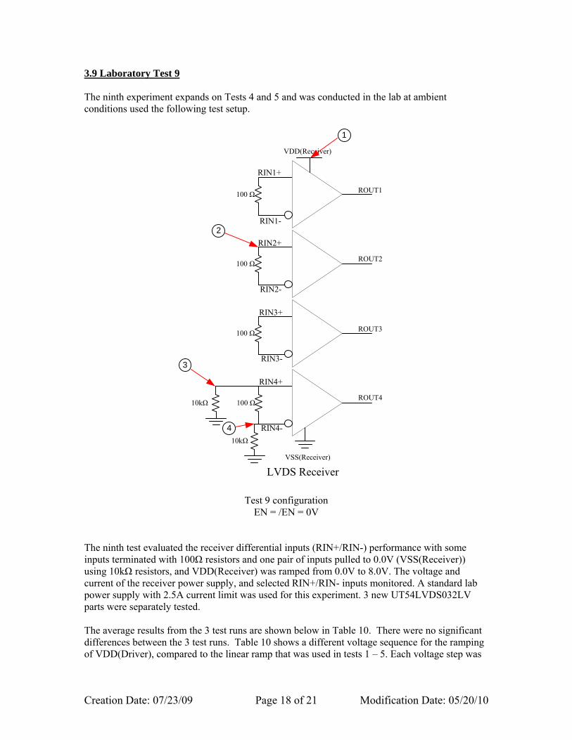
3.9 Laboratory Test 9 The ninth experiment expands on Tests 4 and 5 and was conducted in the lab at ambient conditions used the following test setup.
100 Ω ROUT1
100 Ω ROUT2
100 Ω ROUT3
ROUT4
LVDS Receiver
VDD(Receiver)
1
3
2
VSS(Receiver)
RIN1+
RIN1-
RIN2+
RIN2-
RIN3+
RIN3-
RIN4+
RIN4-
10kΩ
10kΩ
4
100 Ω
Test 9 configuration EN = /EN = 0V
The ninth test evaluated the receiver differential inputs (RIN+/RIN-) performance with some inputs terminated with 100Ω resistors and one pair of inputs pulled to 0.0V (VSS(Receiver)) using 10kΩ resistors, and VDD(Receiver) was ramped from 0.0V to 8.0V. The voltage and current of the receiver power supply, and selected RIN+/RIN- inputs monitored. A standard lab power supply with 2.5A current limit was used for this experiment. 3 new UT54LVDS032LV parts were separately tested. The average results from the 3 test runs are shown below in Table 10. There were no significant differences between the 3 test runs. Table 10 shows a different voltage sequence for the ramping of VDD(Driver), compared to the linear ramp that was used in tests 1 – 5. Each voltage step was

Creation Date: 07/23/09 Page 19 of 21 Modification Date: 05/20/10
held for 15 seconds before moving to the next step, providing more than enough time for any overheating damage to present.
VDD Receiver
(V)
I VDD(Receiver)
(mA)
RIN2+ (V)
Average
RIN3+ (V)
Average
RIN3- (V)
Average Point 1 Point 1 Point 2 Point 3 Point 4
0 0.09 -0.03 -0.03 -0.03 3.3 7.93 2.36 0.01 0.01 3.6 7.98 3.33 0.00 -0.01 4 8.68 3.87 0.03 0.03
4.5 10.22 4.42 0.07 0.05 5 13.61 4.90 0.13 0.11
5.5 20.71 5.39 0.18 0.18 6 33.43 5.87 0.25 0.25
6.5 52.85 6.37 0.37 0.35 7 84.81 6.85 0.48 0.47
7.5 258.86 7.26 0.56 0.54 8 1188.28 0.25 0.27 0.21
Table 10. Test 9 Results
Table 10 (like Tables 5 and 6) indicates the UT54LVDS032LV does propagate receiver supply overvoltages out of its RIN inputs. Although overvoltages can propagated, faults are not propagated as there is insufficient current sourced out of the RIN pins, as calculated from the voltage drop across the 10 kΩ pull-down resistors, to damage or degrade the LVDS outputs per section 4.0. Additionally, at 8V the voltage on the LVDS inputs drops significantly indicating the receivers experience catastrophic failure but the voltage out of the LVDS inputs remains within the recommended operating range when VDD exceeds approximately 8V. Test 9 shows that pull-down resistors could be used to preclude receiver supply overvoltages from propagating to a driver. However, these are not necessary as there is insufficient current to propagate a fault. Also, the LVDS lines would only show the receiver supply overvoltage if the driver was tristated or powered-off, as an active driver would overpower the receiver supply overvoltages and hold the LVDS lines at operating levels.

Creation Date: 07/23/09 Page 20 of 21 Modification Date: 05/20/10
4.0 LVDS I/O Current Reliability Analysis The metal current density design rule for the 0.25μm LVDS technology is 0.55mA/μ at 125°C. The minimum metal on the LVDS inputs and outputs are 8 fingers of 1.36μ metal 1. This allows a DC current of 5.98mA on the LVDS I/O while remaining within allowed specifications. After reviewing the reliability assessment the UT54LVDS031LV and the UT200SpWPHY01 these devices can tolerate 100μA of current per pin indefinitely without damage or degradation for a 15 year mission. This assessment is applicable for the following three driver modes:
VDD = 0V VDD = 3.3V with the LVDS outputs enabled (driving) VDD = 3.3V with the LVDS outputs disabled (tristated)
Additionally, from Table 10, an LVDS receiver experiencing overvoltage could back-drive up to 57μA per LVDS line to an LVDS driver. If all 4 pairs of LVDS lines were connected, a total of approximately 460μA could be back-driven. 460μA is more than an order of magnitude below the 5.98mA threshold. Therefore no faults would be propagated from an LVDS receiver experiencing overvoltages to an LVDS driver. 5.0 Fault Conditions and Results The fault conditions examined in this application note focus on demonstrating the response of Aeroflex LVDS drivers and receivers to voltage stress above the ABSOLUTE MAXIMUM RATING for VDD and the I/O. The tests were preformed with the UT54LVDS031LV and UT54LVDS032LV devices at room temperature (25°C). Tests 1 – 5 were preformed using only 1 device per test, tests 6 – 9 were preformed with 3 devices per test. The tests described above show that overvoltages can be seen on the LVDS I/O but that faults are not propagated because the current sourced over the LVDS lines by the part experiencing the overvoltage is not sufficient to cause damage or degradation to the other LVDS part. The experiments also show that sufficiently high voltage applied to the device resulted in transistor break down causing permanent damage with no overvoltage propagation. The Aeroflex LVDS drivers are current mode outputs with a constant current source capable of driving a 3.5mA nominal current. The results discussed above are not guaranteed by Aeroflex. Any operation outside of the ABSOLUTE MAXIMUM RATINGS as stated in the datasheet and/or SMD may affect device reliability and performance. The lab experiments show that a high voltage fault, above the ABSOLUTE MAXIMUM RATINGS, on the LVDS driver VDD and outputs does not propagate to the rest of the system. The experiments also show that sufficiently high voltage applied to the device resulted in transistor break down causing permanent damage.
Creation Date: 07/23/09 Page 21 of 21 Modification Date: 05/20/10
6.0 References [1] Barry Cook, “SPACEWIRE PHYSICAL LAYER FAULT ISOLATION” Session: Test, SpaceWire Components Short Paper, 4Links Limited, Bletchley Park, MK3 6EB, England [2] European Cooperation for Space Standardization, “ECSS-E-ST-50-12C, SpaceWire - Links, nodes, routers and networks”, July 31, 2008 [3] Telecommunications Industry Association, “Electrical Characteristics of Low Voltage Differential Signaling (LVDS) Interface Circuits ANSI/TIA/EIA-644”, January 30, 2001. [4] Aeroflex Standard Products, UT54LVDS031LV/E Low Voltage Quad Driver Data Sheet, December, 2008 [5] Aeroflex Standard Products, UT54LVDS032LV/E Low Voltage Quad Receiver Data Sheet, December, 2008 [6] Aeroflex Standard Products, UT200SpWPHY01 SpaceWire Physical Layer Transceiver Data Sheet, February, 2008