Embed Size (px)
Citation preview
8/6/2019 ADXL320 acelerómetro
http://slidepdf.com/reader/full/adxl320-acelerometro 1/16
Small and Thin ±5 g iMEMS® Accelerometer
ADXL320
Rev.0
Information furnished by Analog Devices is believed to be accurate and reliable.However, no responsibility is assumed by Analog Devices for its use, nor for anyinfringements of patents or other rights of third parties that may result from its use.Specifications subject to change without notice. No license is granted by implicationor otherwise under any patent or patent rights of Analog Devices. Trademarks andregistered trademarks are the property of their respective owners.
One Technology Way, P.O. Box 9106, Norwood, MA 02062-9106, U.S.A.Tel: 781.329.4700 www.analog.com Fax: 781.326.8703 © 2007 Analog Devices, Inc. All rights reserved.
FEATURESSmall and thin
4 mm × 4 mm × 1.45 mm LFCSP package
2 mg resolution at 60 Hz
Wide supply voltage range: 2.4 V to 5.25 V
Low power: 350 μA at VS = 2.4 V (typ)
Good zero g bias stability
Good sensitivity accuracy
X-axis and Y-axis aligned to within 0.1° (typ)
BW adjustment with a single capacitor
Single-supply operation
10,000 g shock survival
Compatible with Sn/Pb and Pb-free solder processes
APPLICATIONS
Cost-sensitive motion- and tilt-sensing applications
Smart hand-held devices
Mobile phones
Sports and health-related devices
PC security and PC peripherals
GENERAL DESCRIPTION The ADXL320 is a low cost, low power, complete dual-axisaccelerometer with signal conditioned voltage outputs, which isall on a single monolithic IC. The product measuresacceleration with a full-scale range of ±5 g (typical). It can alsomeasure both dynamic acceleration (vibration) and staticacceleration (gravity).
The ADXL320’s typical noise floor is 250 μ g /√Hz, allowingsignals below 2 m g to be resolved in tilt-sensing applicationsusing narrow bandwidths (<60 Hz).
The user selects the bandwidth of the accelerometer using
capacitors CX and CY at the XOUT and YOUT pins. Bandwidths of 0.5 Hz to 2.5 kHz may be selected to suit the application.
The ADXL320 is available in a very thin 4 mm × 4 mm ×1.45 mm, 16-lead, plastic LFCSP.
FUNCTIONAL BLOCK DIAGRAM
0 4 9 9 3 - 0 0 1
ADXL320
SENSOR
+3V
OUTPUTAMP
OUTPUTAMP
COM ST
VS
CDC DEMODAC
AMP
RFILT32kΩ
XOUTCX
YOUTCY
RFILT32kΩ
Figure 1.
8/6/2019 ADXL320 acelerómetro
http://slidepdf.com/reader/full/adxl320-acelerometro 2/16
ADXL320
Rev. 0 | Page 2 of 16
TABLE OF CONTENTS
Specifications..................................................................................... 3
Absolute Maximum Ratings............................................................ 4
ESD Caution.................................................................................. 4
Pin Configuration and Function Descriptions............................. 5
Typical Performance Characteristics (VS = 3.0 V) ....................... 7
Theory of Operation ...................................................................... 11
Performance................................................................................ 11
Applications.....................................................................................12
Power Supply Decoupling .........................................................12
Setting the Bandwidth Using CX and CY ................................. 12
Self-Test ....................................................................................... 12
Design Trade-Offs for Selecting Filter Characteristics: The
Noise/BW Trade-Off.................................................................. 12
Use with Operating Voltages Other than 3 V.......... ...... ....... ...... 13
Use as a Dual-Axis Tilt Sensor ................................................. 13
Outline Dimensions....................................................................... 14
Ordering Guide .......................................................................... 14
REVISION HISTORY
9/04—Revision 0: Initial Version
8/6/2019 ADXL320 acelerómetro
http://slidepdf.com/reader/full/adxl320-acelerometro 3/16
ADXL320
Rev. 0 | Page 3 of 16
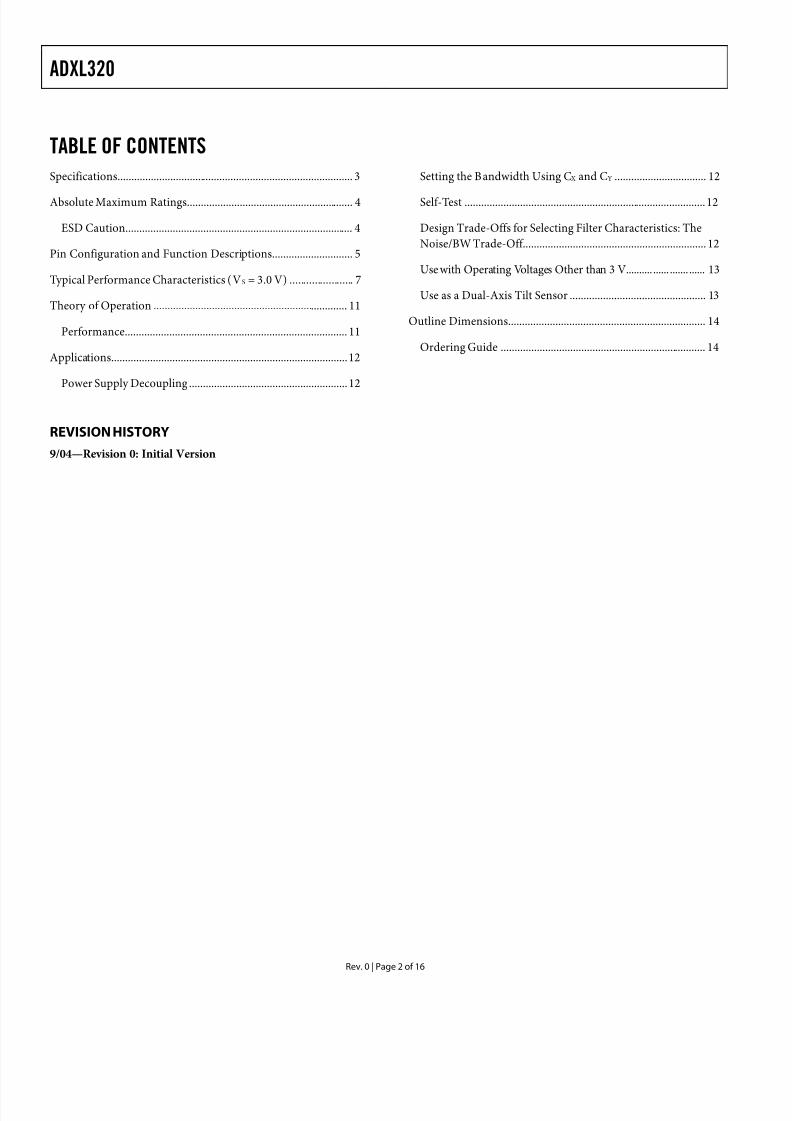
SPECIFICATIONS1
TA = 25°C, VS = 3 V, CX = CY = 0.1 μF, Acceleration = 0 g , unless otherwise noted.
Table 1.
Parameter Conditions Min Typ Max Unit
SENSOR INPUT Each axis
Measurement Range ±5 g
Nonlinearity % of full scale ±0.2 %Package Alignment Error ±1 Degrees
Alignment Error X sensor to Y sensor ±0.1 Degrees
Cross Axis Sensitivity ±2 %
SENSITIVITY (RATIOMETRIC)2 Each axis
Sensitivity at XOUT, YOUT VS = 3 V 156 174 192 mV/g
Sensitivity Change due to Temperature3 VS = 3 V 0.01 %/°C
ZERO g BIAS LEVEL (RATIOMETRIC) Each axis
0 g Voltage at XOUT, YOUT VS = 3 V 1.3 1.5 1.7 V
0 g Offset Versus Temperature ±0.6 mg /°CNOISE PERFORMANCE
Noise Density @ 25°C 250 μg /√Hz rms
FREQUENCY RESPONSE4
CX, CY Range5 0.002 10 μF
RFILT Tolerance 32 ± 15% kΩSensor Resonant Frequency 5.5 kHz
SELF-TESTT
6
Logic Input Low 0.6 V
Logic Input High 2.4 VST Input Resistance to Ground 50 kΩ
Output Change at XOUT, YOUT Self-test 0 to 1 55 mV
OUTPUT AMPLIFIEROutput Swing Low No load 0.3 V
Output Swing High No load 2.5 V
POWER SUPPLY
Operating Voltage Range 2.4 5.25 V
Quiescent Supply Current 0.48 mA
Turn-On Time7 20 ms
TEMPERATURE
Operating Temperature Range −20 70 °C
1 All minimum and maximum specifications are guaranteed. Typical specifications are not guaranteed.2 Sensitivity is essentially ratiometric to VS. For VS = 2.7 V to 3.3 V, sensitivity is 154 mV/V/g to 194 mV/V/g typical.3 Defined as the output change from ambient-to-maximum temperature or ambient-to-minimum temperature.4 Actual frequency response controlled by user-supplied external capacitor (CX, CY).5 Bandwidth = 1/(2 × π × 32 kΩ × C). For CX, CY = 0.002 μF, bandwidth = 2500 Hz. For CX, CY = 10 μF, bandwidth = 0.5 Hz. Minimum/maximum values are not tested.6 Self-test response changes cubically with VS.7 Larger values of CX, CY increase turn-on time. Turn-on time is approximately 160 × C X or CY + 4 ms, where CX, CY are in μF.
8/6/2019 ADXL320 acelerómetro
http://slidepdf.com/reader/full/adxl320-acelerometro 4/16
ADXL320
Rev. 0 | Page 4 of 16
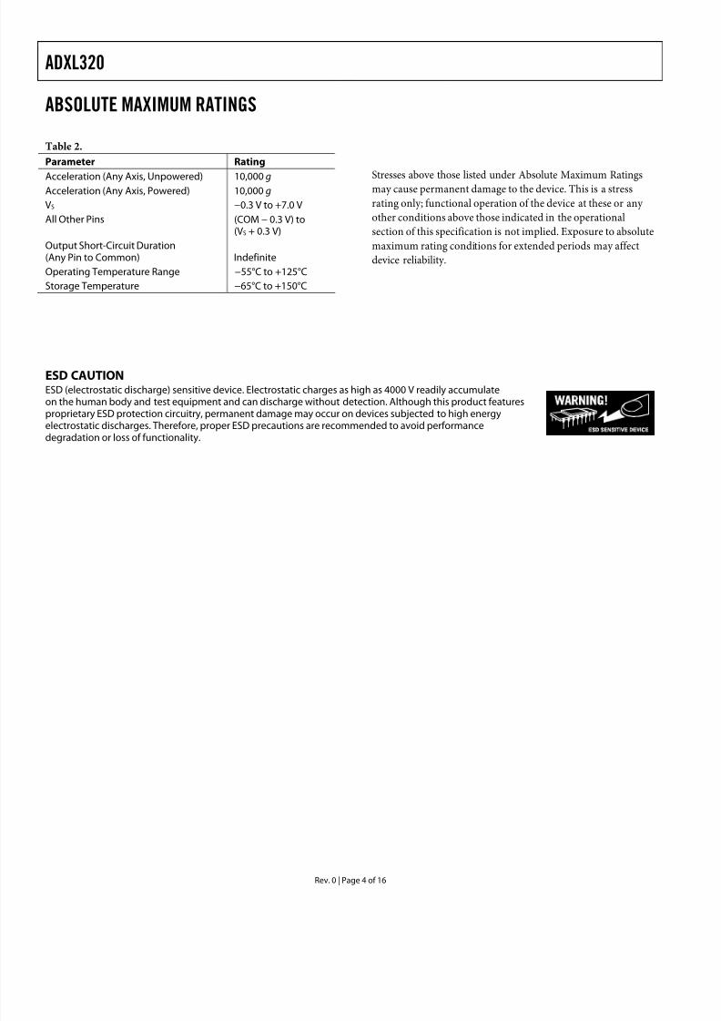
ABSOLUTE MAXIMUM RATINGS
Table 2.
Parameter Rating
Acceleration (Any Axis, Unpowered) 10,000 g Acceleration (Any Axis, Powered) 10,000 g VS −0.3 V to +7.0 V
All Other Pins (COM − 0.3 V) to(VS + 0.3 V)
Output Short-Circuit Duration(Any Pin to Common) Indefinite
Operating Temperature Range −55°C to +125°CStorage Temperature −65°C to +150°C
Stresses above those listed under Absolute Maximum Ratingsmay cause permanent damage to the device. This is a stressrating only; functional operation of the device at these or any other conditions above those indicated in the operationalsection of this specification is not implied. Exposure to absolutemaximum rating conditions for extended periods may affectdevice reliability.
ESD CAUTIONESD (electrostatic discharge) sensitive device. Electrostatic charges as high as 4000 V readily accumulateon the human body and test equipment and can discharge without detection. Although this product featuresproprietary ESD protection circuitry, permanent damage may occur on devices subjected to high energyelectrostatic discharges. Therefore, proper ESD precautions are recommended to avoid performancedegradation or loss of functionality.
8/6/2019 ADXL320 acelerómetro
http://slidepdf.com/reader/full/adxl320-acelerometro 5/16
ADXL320
Rev. 0 | Page 5 of 16
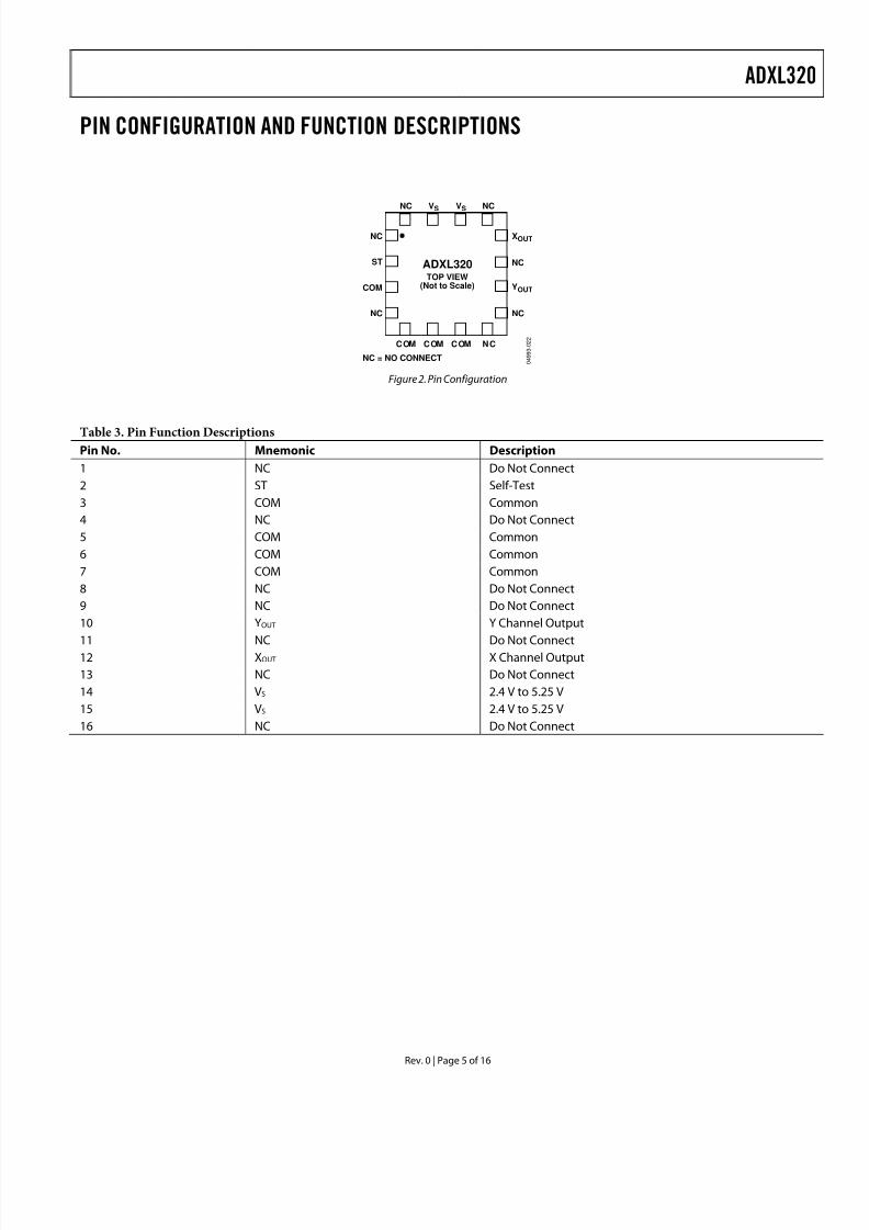
PIN CONFIGURATION AND FUNCTION DESCRIPTIONS
NC XOUT
ST NC
COM YOUT
NC NC
COM COM COM NC
NC VS VS NC
NC = NO CONNECT
ADXL320TOP VIEW
(Not to Scale)
0 4 9 9 3 - 0 2 2
Figure 2. Pin Configuration
Table 3. Pin Function DescriptionsPin No. Mnemonic Description
1 NC Do Not Connect
2 ST Self-Test
3 COM Common4 NC Do Not Connect
5 COM Common
6 COM Common
7 COM Common
8 NC Do Not Connect9 NC Do Not Connect
10 YOUT Y Channel Output
11 NC Do Not Connect12 XOUT X Channel Output13 NC Do Not Connect
14 VS 2.4 V to 5.25 V
15 VS 2.4 V to 5.25 V
16 NC Do Not Connect
8/6/2019 ADXL320 acelerómetro
http://slidepdf.com/reader/full/adxl320-acelerometro 6/16
ADXL320
Rev. 0 | Page 6 of 16
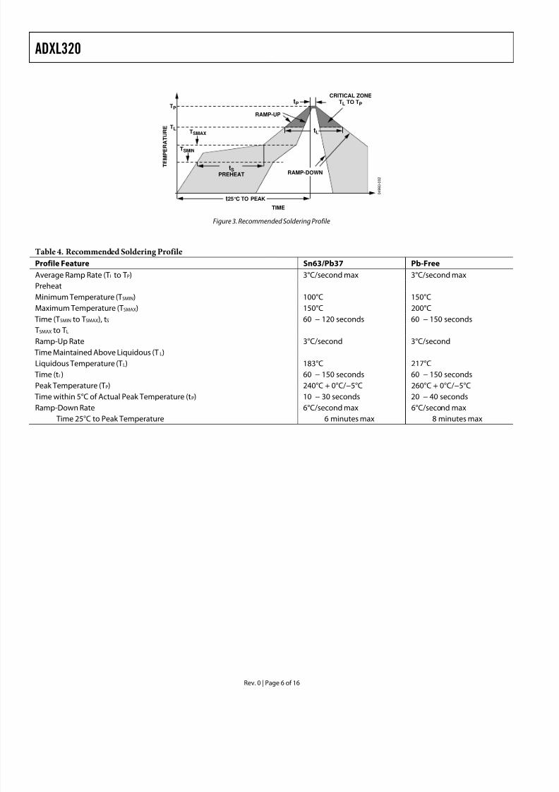
0 4 9 9 3 - 0 0 2
tP
tL
t25°C TO PEAK
tS
PREHEAT
CRITICAL ZONE
TL TO TP
T E M P E R A T
U R E
TIME
RAMP-DOWN
RAMP-UP
TSMIN
TSMAX
TP
TL
Figure 3. Recommended Soldering Profile
Table 4. Recommended Soldering Profile
Profile Feature Sn63/Pb37 Pb-Free
Average Ramp Rate (TL to TP) 3°C/second max 3°C/second maxPreheat
Minimum Temperature (TSMIN) 100°C 150°C
Maximum Temperature (TSMAX) 150°C 200°C
Time (TSMIN to TSMAX), tS 60 − 120 seconds 60 − 150 seconds
TSMAX to TL
Ramp-Up Rate 3°C/second 3°C/second
Time Maintained Above Liquidous (T L)
Liquidous Temperature (TL) 183°C 217°C
Time (tL) 60 − 150 seconds 60 − 150 seconds
Peak Temperature (TP) 240°C + 0°C/−5°C 260°C + 0°C/−5°C
Time within 5°C of Actual Peak Temperature (tP) 10 − 30 seconds 20 − 40 seconds
Ramp-Down Rate 6°C/second max 6°C/second max
Time 25°C to Peak Temperature 6 minutes max 8 minutes max
8/6/2019 ADXL320 acelerómetro
http://slidepdf.com/reader/full/adxl320-acelerometro 7/16
ADXL320
Rev. 0 | Page 7 of 16
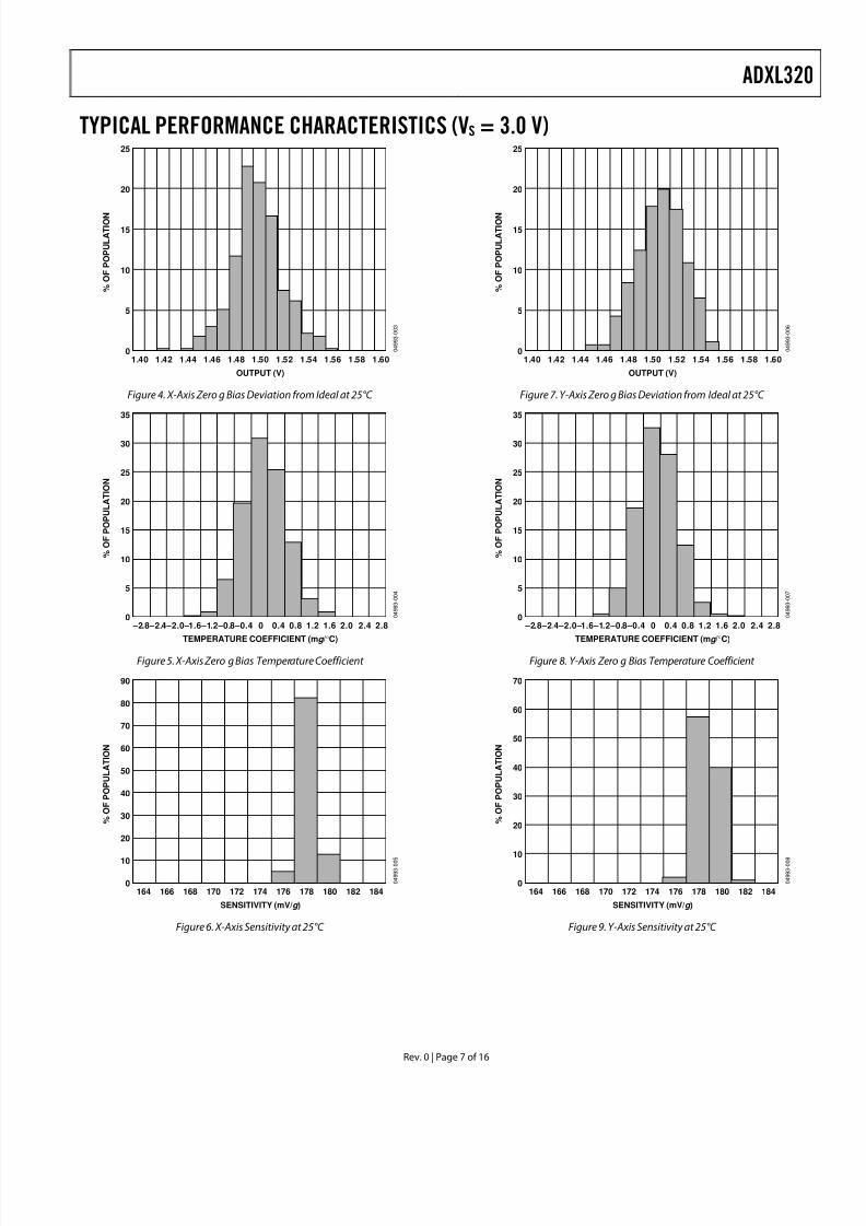
TYPICAL PERFORMANCE CHARACTERISTICS (VS = 3.0 V)25
0
5
10
15
20
1.40 1.42 1.44 1.46 1.48 1.50 1.52 1.54 1.56 1.58 1.60
0 4 9 9 3 - 0 0 3
OUTPUT (V)
% O
F P O P U L A T I O N
Figure 4. X-Axis Zero g Bias Deviation from Ideal at 25°C
35
0
5
10
15
20
25
30
–2.8–2.4–2.0–1.6–1.2–0.8–0.4 0 0.4 0.8 1.2 1.6 2.0 2.4 2.8
0 4 9 9 3 - 0 0 4
TEMPERATURE COEFFICIENT (mg /°C)
% O
F P O P U L A T I O N
Figure 5. X-Axis Zero g Bias Temperature Coefficient
90
0
10
20
30
40
50
70
80
60
164 184182180178176174172170168166
0 4 9 9 3 - 0 0 5
SENSITIVITY (mV/g )
% O
F P O P U L A T I O N
Figure 6. X-Axis Sensitivity at 25°C
25
0
5
10
15
20
1.40 1.42 1.44 1.46 1.48 1.50 1.52 1.54 1.56 1.58 1.60
0 4 9 9 3 - 0 0 6
OUTPUT (V)
% O
F P O P U L A T I O N
Figure 7. Y-Axis Zero g Bias Deviation from Ideal at 25°C
35
0
5
10
15
20
25
30
–2.8–2.4–2.0–1.6–1.2–0.8–0.4 0 0.4 0.8 1.2 1.6 2.0 2.4 2.8
0 4 9 9 3 - 0 0 7
TEMPERATURE COEFFICIENT (mg /°C)
% O
F P O P U L A T I O N
Figure 8. Y-Axis Zero g Bias Temperature Coefficient
70
0
10
20
30
40
50
60
164 184182180178176174172170168166
0 4 9 9 3 - 0 0 8
SENSITIVITY (mV/g )
% O
F P O P U L A T I O N
Figure 9. Y-Axis Sensitivity at 25°C
8/6/2019 ADXL320 acelerómetro
http://slidepdf.com/reader/full/adxl320-acelerometro 8/16
ADXL320
Rev. 0 | Page 8 of 16
1.54
1.53
1.52
1.51
1.50
1.49
1.48
1.47
1.46 –30 –20 –10 0 10 20 30 40 50 60 70 80
0 4 9 9 3 - 0 0 9
TEMPERATURE (°C)
O U T P U T ( S C A L E
= 1 7 4 m V / g )
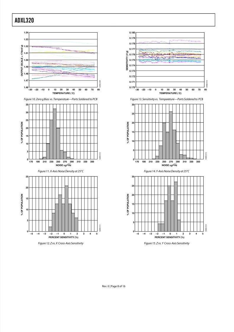
Figure 10. Zero g Bias vs. Temperature—Parts Soldered to PCB
35
30
25
20
15
10
5
0170 190 210 230 250 270 290 310 330 350
0 4 9 9 3 - 0 1 0
NOISE ug / Hz
% O
F P O P U L A T I O N
Figure 11. X-Axis Noise Density at 25°C
25
20
15
10
5
0 –5 –4 –3 –2 –1 0 1 2 3 4 5
0 4 9 9 3 - 0 1 1
PERCENT SENSITIVITY (%)
% O
F P O P U L A T I O N
Figure 12. Z vs. X Cross-Axis Sensitivity
0.180
0.170
0.171
0.172
0.173
0.174
0.175
0.176
0.177
0.178
0.179
–30 –20 –10 0 10 20 30 40 50 60 70 80
0 4 9 9 3 - 0 1 2
TEMPERATURE (°C)
S E N S I T I V I T Y ( V / g )
Figure 13. Sensitivity vs. Temperature—Parts Soldered to PCB
30
25
20
15
10
5
0170 190 210 230 250 270 290 310 330 350
0 4 9 9 3 - 0 1 3
NOISE ug / Hz
% O
F P O P U L A T I O N
Figure 14. Y-Axis Noise Density at 25°C
30
25
20
15
10
5
0 –5 –4 –3 –2 –1 0 1 2 3 4 5
0 4 9 9 3 - 0 1 4
PERCENT SENSITIVITY (%)
% O
F P O P U L A T I O N
Figure 15. Z vs. Y Cross-Axis Sensitivity
8/6/2019 ADXL320 acelerómetro
http://slidepdf.com/reader/full/adxl320-acelerometro 9/16
ADXL320
Rev. 0 | Page 9 of 16
60
50
40
30
20
10
035 7570656055504540
0 4 9 9 3 - 0 1 5
SELF-TEST (mV)
% O
F P O P U L
A T I O N
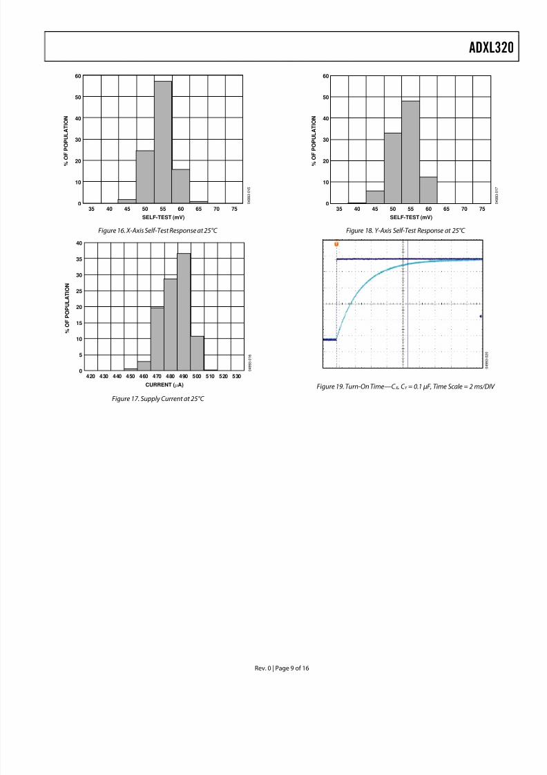
Figure 16. X-Axis Self-Test Response at 25°C
40
35
30
25
20
15
10
5
0420 430 440 450 460 470 480 490 500 510 520 530
0 4 9 9 3 - 0 1 6
CURRENT (μA)
% O
F P O P U L A T I O N
Figure 17. Supply Current at 25°C
60
50
40
30
20
10
035 7570656055504540
0 4 9 9 3 - 0 1 7
SELF-TEST (mV)
% O
F P O P U L
A T I O N
Figure 18. Y-Axis Self-Test Response at 25°C
0 4 9 9 3 - 0 2 0
Figure 19. Turn-On Time—C X , C Y = 0.1 μF, Time Scale = 2 ms/DIV
8/6/2019 ADXL320 acelerómetro
http://slidepdf.com/reader/full/adxl320-acelerometro 10/16
ADXL320
Rev. 0 | Page 10 of 16
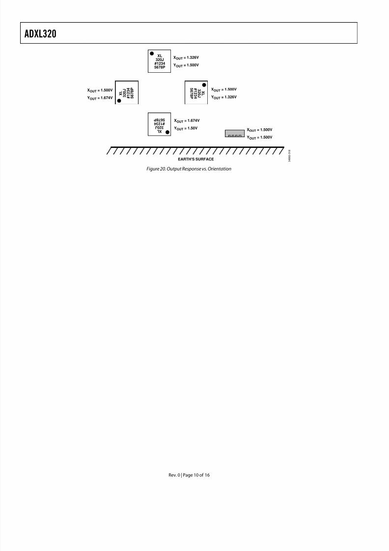
0 4 9 9 3 - 0 1 8
XOUT = 1.500V
YOUT = 1.500V
XOUT = 1.500V
YOUT = 1.326V
XOUT = 1.326V
YOUT = 1.500V
XOUT = 1.674V
YOUT = 1.50V
XOUT = 1.500V
YOUT = 1.674V
EARTH'S SURFACE
XL320J
#12345678P
X L
3 2 0 J
# 1 2
3 4
5 6 7
8 P X L
3
2 0 J
# 1 2 3 4
5 6 7 8 P
X L
3 2 0 J
# 1 2 3 4
5 6 7 8 P
Figure 20. Output Response vs. Orientation
8/6/2019 ADXL320 acelerómetro
http://slidepdf.com/reader/full/adxl320-acelerometro 11/16
ADXL320
Rev. 0 | Page 11 of 16
THEORY OF OPERATIONThe ADXL320 is a complete acceleration measurement systemon a single monolithic IC. The ADXL320 has a measurementrange of ±5 g . It contains a polysilicon surface-micromachinedsensor and signal conditioning circuitry to implement an open-loop acceleration measurement architecture. The output signalsare analog voltages that are proportional to acceleration. Theaccelerometer measures static acceleration forces, such asgravity, which allows it to be used as a tilt sensor.
The sensor is a polysilicon surface-micromachined structurebuilt on top of a silicon wafer. Polysilicon springs suspend thestructure over the surface of the wafer and provide a resistanceagainst acceleration forces. Deflection of the structure ismeasured using a differential capacitor that consists of independent fixed plates and plates attached to the movingmass. The fixed plates are driven by 180° out-of-phase squarewaves. Acceleration deflects the beam and unbalances thedifferential capacitor, resulting in an output square wave whoseamplitude is proportional to acceleration. Phase-sensitivedemodulation techniques are then used to rectify the signal anddetermine the direction of the acceleration.
The demodulator’s output is amplified and brought off-chipthrough a 32 kΩ resistor. The user then sets the signalbandwidth of the device by adding a capacitor. This filteringimproves measurement resolution and helps prevent aliasing.
PERFORMANCE
Rather than using additional temperature compensationcircuitry, innovative design techniques have been used to ensurehigh performance is built-in. As a result, there is neitherquantization error nor nonmonotonic behavior, andtemperature hysteresis is very low (typically less than 3 m g overthe −20°C to +70°C temperature range).
Figure 10 shows the zero g output performance of eight parts(X- and Y-axis) over a −20°C to +70°C temperature range.
Figure 13 demonstrates the typical sensitivity shift over
temperature for supply voltages of 3 V. This is typically betterthan ±1% over the −20°C to +70°C temperature range.
8/6/2019 ADXL320 acelerómetro
http://slidepdf.com/reader/full/adxl320-acelerometro 12/16
ADXL320
Rev. 0 | Page 12 of 16
APPLICATIONSPOWER SUPPLY DECOUPLING
For most applications, a single 0.1 μF capacitor, C DC, adequately decouples the accelerometer from noise on the power supply.
However, in some cases, particularly where noise is present atthe 140 kHz internal clock frequency (or any harmonicthereof), noise on the supply may cause interference on theADXL320 output. If additional decoupling is needed, a 100 Ω(or smaller) resistor or ferrite bead may be inserted in thesupply line. Additionally, a larger bulk bypass capacitor (in the1 μF to 4.7 μF range) may be added in parallel to CDC.
SETTING THE BANDWIDTH USING CX AND CY
The ADXL320 has provisions for band-limiting the XOUT andYOUT pins. Capacitors must be added at these pins to implementlow-pass filtering for antialiasing and noise reduction. Theequation for the 3 dB bandwidth is
F −3 dB = 1/(2π(32 kΩ) × C( X , Y ))
or more simply,
F –3 dB = 5 μF /C( X , Y )
The tolerance of the internal resistor (RFILT) typically varies asmuch as ±15% of its nominal value (32 kΩ), and the bandwidth
varies accordingly. A minimum capacitance of 2000 pF for CX and CY is required in all cases.
Table 5. Filter Capacitor Selection, CX and CY
Bandwidth (Hz) Capacitor (μF)
1 4.7
10 0.47
50 0.10
100 0.05
200 0.027500 0.01
SELF-TEST
The ST pin controls the self-test feature. When this pin is set toVS, an electrostatic force is exerted on the accelerometer beam.The resulting movement of the beam allows the user to test if the accelerometer is functional. The typical change in output is
315 m g (corresponding to 55 mV). This pin may be left open-circuit or connected to common (COM) in normal use.
The ST pin should never be exposed to voltages greater thanVS + 0.3 V. If this cannot be guaranteed due to the systemdesign (for instance, if there are multiple supply voltages), thena low VF clamping diode between ST and VS is recommended.
DESIGN TRADE-OFFS FOR SELECTING FILTERCHARACTERISTICS: THE NOISE/BW TRADE-OFF
The accelerometer bandwidth selected ultimately determines
the measurement resolution (smallest detectable acceleration).Filtering can be used to lower the noise floor, which improvesthe resolution of the accelerometer. Resolution is dependent onthe analog filter bandwidth at XOUT and YOUT.
The output of the ADXL320 has a typical bandwidth of 2.5 kHz.The user must filter the signal at this point to limit aliasingerrors. The analog bandwidth must be no more than half theA/D sampling frequency to minimize aliasing. The analogbandwidth may be further decreased to reduce noise andimprove resolution.
The ADXL320 noise has the characteristics of white Gaussiannoise, which contributes equally at all frequencies and isdescribed in terms of μ g /√Hz (the noise is proportional to thesquare root of the accelerometer’s bandwidth). The user shouldlimit bandwidth to the lowest frequency needed by theapplication in order to maximize the resolution and dynamicrange of the accelerometer.
With the single-pole, roll-off characteristic, the typical noise of the ADXL320 is determined by
)1.6()μg/(250 ××= BW Hz rmsNoise
At 100 Hz bandwidth the noise will be
mg3.2)1.6100()μg/(250 =××= Hz rmsNoise
Often, the peak value of the noise is desired. Peak-to-peak noisecan only be estimated by statistical methods. Table 6 is usefulfor estimating the probabilities of exceeding various peak
values, given the rms value.
Table 6. Estimation of Peak-to-Peak Noise
Peak-to-Peak Value% of Time That Noise ExceedsNominal Peak-to-Peak Value
2 × rms 32
4 × rms 4.6
6 × rms 0.27
8 × rms 0.006
8/6/2019 ADXL320 acelerómetro
http://slidepdf.com/reader/full/adxl320-acelerometro 13/16
ADXL320
Rev. 0 | Page 13 of 16
Peak-to-peak noise values give the best estimate of theuncertainty in a single measurement. Table 7 gives the typicalnoise output of the ADXL320 for various CX and CY values.
Table 7. Filter Capacitor Selection (CX , CY)
Bandwidth
(Hz)
CX, CY
(μF)
RMS Noise
(mg)
Peak-to-Peak Noise
Estimate (mg)10 0.47 1.0 6
50 0.1 2.25 13.5
100 0.047 3.2 18.9
500 0.01 7.1 42.8
USE WITH OPERATING VOLTAGES OTHER THAN 3 V
The ADXL320 is tested and specified at VS = 3 V; however, itcan be powered with VS as low as 2.4 V or as high as 5.25 V.Note that some performance parameters change as the supply
voltage is varied.
The ADXL320 output is ratiometric, so the output sensitivity
(or scale factor) varies proportionally to supply voltage. At VS =5 V, the output sensitivity is typically 312 mV/ g . At VS = 2.4 V,the output sensitivity is typically 135 mV/ g .
The zero g bias output is also ratiometric, so the zero g output isnominally equal to VS/2 at all supply voltages.
The output noise is not ratiometric but is absolute in volts;therefore, the noise density decreases as the supply voltageincreases. This is because the scale factor (mV/ g ) increaseswhile the noise voltage remains constant. At VS = 5 V, the noisedensity is typically 150 μ g /√Hz, while at VS = 2.4 V, the noisedensity is typically 300 μ g /√Hz,
Self-test response in g is roughly proportional to the square of the supply voltage. However, when ratiometricity of sensitivity is factored in with supply voltage, the self-test response in voltsis roughly proportional to the cube of the supply voltage. Forexample, at VS = 5 V, the self-test response for the ADXL320 isapproximately 250 mV. At VS = 2.4 V, the self-test response isapproximately 25 mV.
The supply current decreases as the supply voltage decreases.Typical current consumption at VS = 5 V is 750 μA, and typicalcurrent consumption at VS = 2.4 V is 350 μA.
USE AS A DUAL-AXIS TILT SENSOR
Tilt measurement is one of the ADXL320’s most popularapplications. An accelerometer uses the force of gravity as aninput vector to determine the orientation of an object in space.
An accelerometer is most sensitive to tilt when its sensitive axisis perpendicular to the force of gravity (that is, when it isparallel to the earth’s surface). At this orientation, its sensitivity to changes in tilt is highest. When the accelerometer is orientedon axis to gravity (near its +1 g or −1 g reading), the change inoutput acceleration per degree of tilt is negligible. When theaccelerometer is perpendicular to gravity, its output changesnearly 17.5 m g per degree of tilt. At 45°, its output changes atonly 12.2 m g per degree of tilt, and resolution declines.
Converting Acceleration to Tilt
When the accelerometer is oriented so both its X-axis andY-axis are parallel to the earth’s surface, it can be used as a 2-
axis tilt sensor with both a roll axis and pitch axis. Once theoutput signal from the accelerometer has been converted to anacceleration that varies between −1 g and +1 g , the output tilt indegrees is calculated as
PITCH = ASIN ( A X /1 g )
ROLL = ASIN ( AY /1 g )
Be sure to account for overranges. It is possible for theaccelerometers to output a signal greater than ±1 g due to
vibration, shock, or other accelerations.

8/6/2019 ADXL320 acelerómetro
http://slidepdf.com/reader/full/adxl320-acelerometro 14/16

8/6/2019 ADXL320 acelerómetro
http://slidepdf.com/reader/full/adxl320-acelerometro 15/16
ADXL320
Rev. 0 | Page 15 of 16
NOTES

8/6/2019 ADXL320 acelerómetro
http://slidepdf.com/reader/full/adxl320-acelerometro 16/16
ADXL320
Rev. 0 | Page 16 of 16
NOTES
© 2007 Analog Devices, Inc. All rights reserved. Trademarks and registered trademarks are the property of their respective owners.
D04993–0–6/07(0)

![PROYECTO FIN DE CARRERA - bibing.us.esbibing.us.es/proyectos/abreproy/12217/fichero/Javier+Paradela... · SEFBA (Sistema de Estabilización de Ferrocarriles Basado en Acelerómetro)]](https://img.dokumen.tips/doc/110x75/5b89d6477f8b9abe1e8e7bf3/proyecto-fin-de-carrera-paradela-sefba-sistema-de-estabilizacion-de-ferrocarriles.jpg)