Embed Size (px)
Citation preview
Hewlett PackardLabs
Advanced Packaging for Silicon Photonic Interconnects
M. Ashkan SeyediLarge-Scale Integrated PhotonicsHewlett Packard Labs, Palo Alto, CA
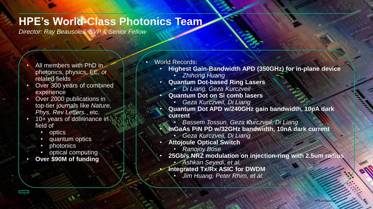
HPE’s World-Class Photonics TeamDirector: Ray Beausoleil, SVP & Senior Fellow
HPE Confidential 2
• All members with PhD in photonics, physics, EE, or related fields
• Over 300 years of combined experience
• Over 2000 publications in top-tier journals like Nature, Phys. Rev Letters., etc.
• 10+ years of dominance in field of
• optics • quantum optics • photonics• optical computing
• Over $90M of funding
• World Records:• Highest Gain-Bandwidth APD (350GHz) for in-plane device
• Zhihong Huang• Quantum Dot-based Ring Lasers
• Di Liang, Geza Kurczveil• Quantum Dot on Si comb lasers
• Geza Kurczveil, Di Liang• Quantum Dot APD w/240GHz gain bandwidth, 10pA dark
current• Bassem Tossun, Geza Kurczveil, Di Liang
• InGaAs PiN PD w/32GHz bandwidth, 10nA dark current• Geza Kurczveil, Di Liang
• Attojoule Optical Switch• Ranojoy Bose
• 25Gb/s NRZ modulation on injection-ring with 2.5um radius• Ashkan Seyedi, et al.
• Integrated Tx/Rx ASIC for DWDM• Jim Huang, Peter Rhim, et al.
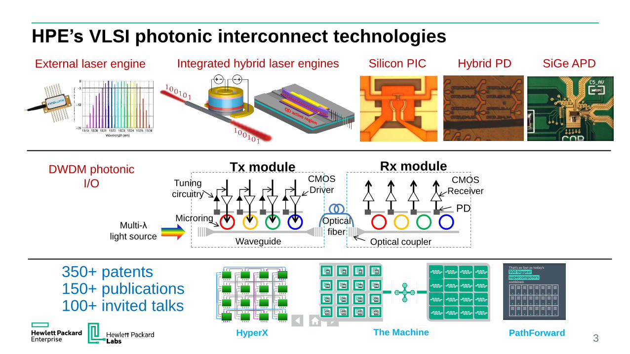
HPE’s VLSI photonic interconnect technologies
3
Integrated hybrid laser engines
DWDM photonic
I/O
HyperX
SiGe APDSilicon PIC
Multi-λ
light source
Optical
fiber
CMOS
DriverTuning
circuitry
Waveguide
Microring
Tx module
Optical coupler
CMOS
Receiver
PD
Rx module
External laser engine Hybrid PD
The Machine PathForward
350+ patents150+ publications100+ invited talks
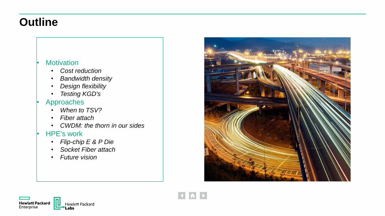
Outline
• Motivation• Cost reduction
• Bandwidth density
• Design flexibility
• Testing KGD's
• Approaches• When to TSV?
• Fiber attach
• CWDM: the thorn in our sides
• HPE's work• Flip-chip E & P Die
• Socket Fiber attach
• Future vision
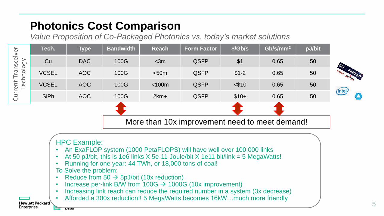
Value Proposition of Co-Packaged Photonics vs. today’s market solutions
5
Tech. Type Bandwidth Reach Form Factor $/Gb/s Gb/s/mm2 pJ/bit
Cu DAC 100G <3m QSFP $1 0.65 50
VCSEL AOC 100G <50m QSFP $1-2 0.65 50
VCSEL AOC 100G <100m QSFP <$10 0.65 50
SiPh AOC 100G 2km+ QSFP $10+ 0.65 50
Photonics Cost Comparison
More than 10x improvement need to meet demand!
HPC Example:• An ExaFLOP system (1000 PetaFLOPS) will have well over 100,000 links• At 50 pJ/bit, this is 1e6 links X 5e-11 Joule/bit X 1e11 bit/link = 5 MegaWatts! • Running for one year: 44 TWh, or 18,000 tons of coal! To Solve the problem: • Reduce from 50 5pJ/bit (10x reduction)• Increase per-link B/W from 100G 1000G (10x improvement)• Increasing link reach can reduce the required number in a system (3x decrease)• Afforded a 300x reduction!! 5 MegaWatts becomes 16kW…much more friendly
6/26/2019
HPE Confidential
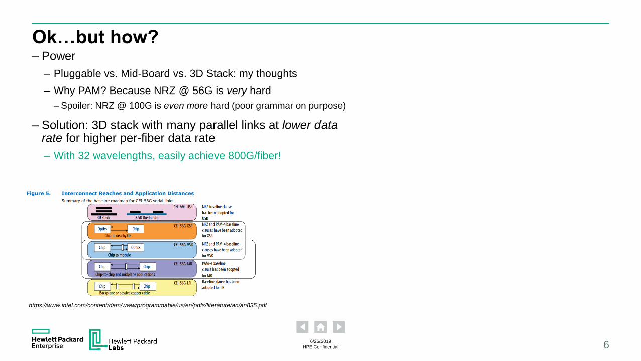
Ok…but how?– Power
– Pluggable vs. Mid-Board vs. 3D Stack: my thoughts
– Why PAM? Because NRZ @ 56G is very hard
– Spoiler: NRZ @ 100G is even more hard (poor grammar on purpose)
– Solution: 3D stack with many parallel links at lower data rate for higher per-fiber data rate
– With 32 wavelengths, easily achieve 800G/fiber!
6
https://www.intel.com/content/dam/www/programmable/us/en/pdfs/literature/an/an835.pdf
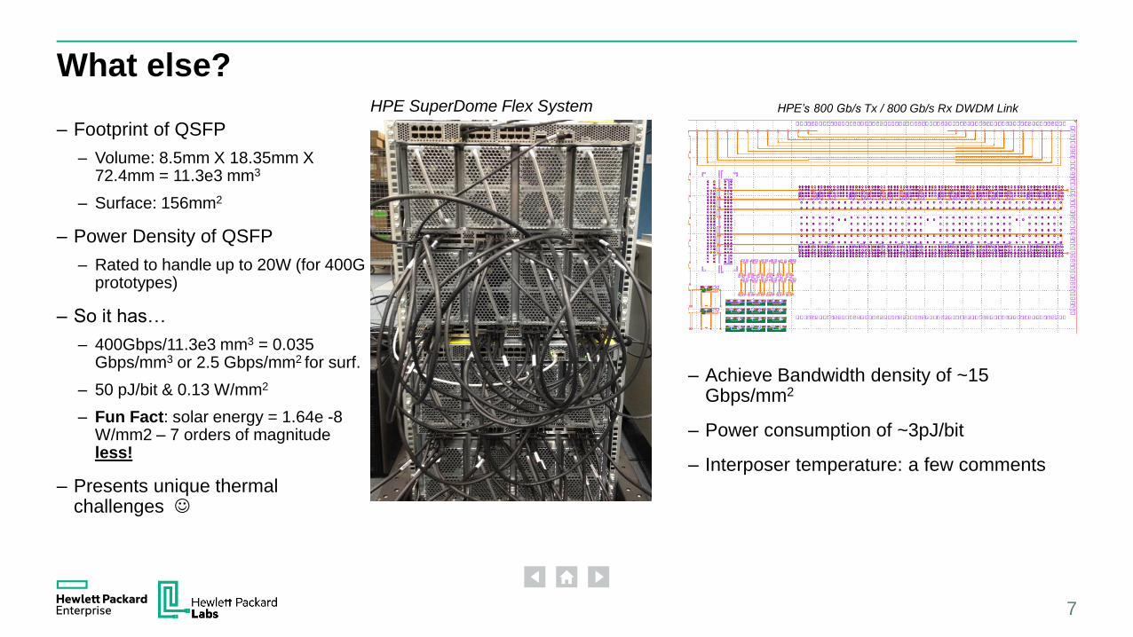
What else?
– Footprint of QSFP
– Volume: 8.5mm X 18.35mm X 72.4mm = 11.3e3 mm3
– Surface: 156mm2
– Power Density of QSFP
– Rated to handle up to 20W (for 400G prototypes)
– So it has…
– 400Gbps/11.3e3 mm3 = 0.035 Gbps/mm3 or 2.5 Gbps/mm2 for surf.
– 50 pJ/bit & 0.13 W/mm2
– Fun Fact: solar energy = 1.64e -8 W/mm2 – 7 orders of magnitude less!
– Presents unique thermal challenges
– Achieve Bandwidth density of ~15 Gbps/mm2
– Power consumption of ~3pJ/bit
– Interposer temperature: a few comments
7
HPE’s 800 Gb/s Tx / 800 Gb/s Rx DWDM LinkHPE SuperDome Flex System
6/26/2019
HPE Confidential
A few words about assembly & associated cost
– If part is expensive to build, add more capability (i.e. bandwidth)
– How to commit known good die to package?
8
Goal: an interconnect that costs less than $0.1/Gbps
6/26/2019
HPE Confidential
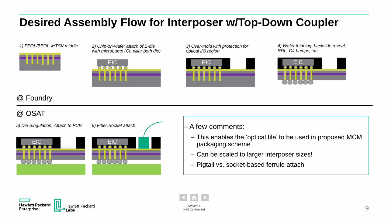
Desired Assembly Flow for Interposer w/Top-Down Coupler
– A few comments:
– This enables the ‘optical tile’ to be used in proposed MCM packaging scheme
– Can be scaled to larger interposer sizes!
– Pigtail vs. socket-based ferrule attach
9
1) FEOL/BEOL w/TSV middle 2) Chip-on-wafer attach of E-die with microbump (Cu pillar both die)
EIC
3) Over-mold with protection for optical I/O region
EIC
4) Wafer thinning, backside reveal, RDL, C4 bumps, etc.
EIC
@ Foundry
@ OSAT
5) Die Singulation, Attach to PCB
EIC
6) Fiber Socket attach
EIC
6/26/2019
HPE Confidential
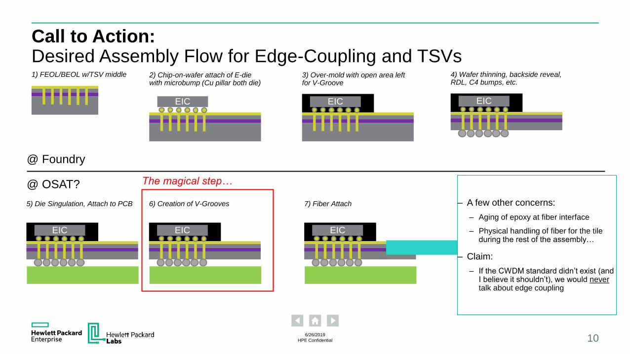
Call to Action:Desired Assembly Flow for Edge-Coupling and TSVs
10
1) FEOL/BEOL w/TSV middle 2) Chip-on-wafer attach of E-die with microbump (Cu pillar both die)
EIC
3) Over-mold with open area left for V-Groove
EIC
4) Wafer thinning, backside reveal, RDL, C4 bumps, etc.
EIC
@ Foundry
@ OSAT?
5) Die Singulation, Attach to PCB
EIC
6) Creation of V-Grooves
EIC
7) Fiber Attach
EIC
The magical step…
– A few other concerns:
– Aging of epoxy at fiber interface
– Physical handling of fiber for the tile during the rest of the assembly…
– Claim:
– If the CWDM standard didn’t exist (and I believe it shouldn’t), we would nevertalk about edge coupling
6/26/2019
HPE Confidential
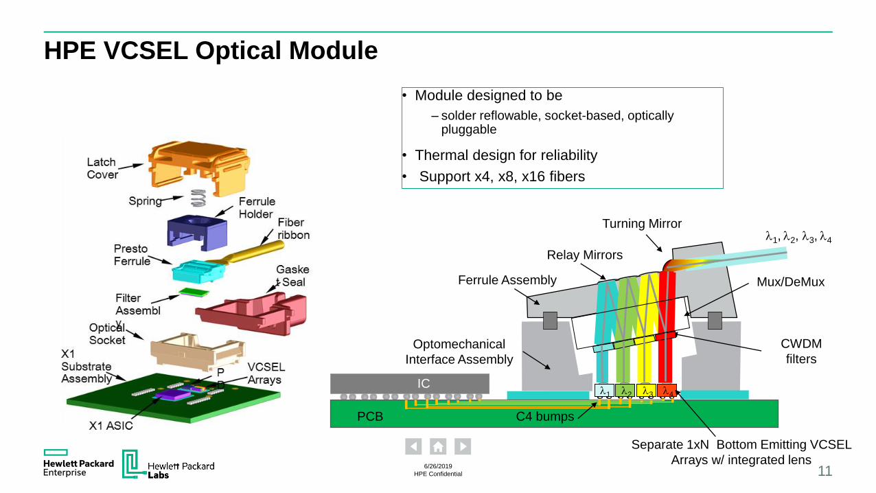
HPE VCSEL Optical Module
• Module designed to be
– solder reflowable, socket-based, optically pluggable
• Thermal design for reliability
• Support x4, x8, x16 fibers
11
l1, l2, l3, l4
CWDM
filtersOptomechanical
Interface Assembly
Separate 1xN Bottom Emitting VCSEL
Arrays w/ integrated lens
Mux/DeMux
Relay Mirrors
l2 l4l1 l3
IC
C4 bumpsPCB
Turning Mirror
Ferrule Assembly
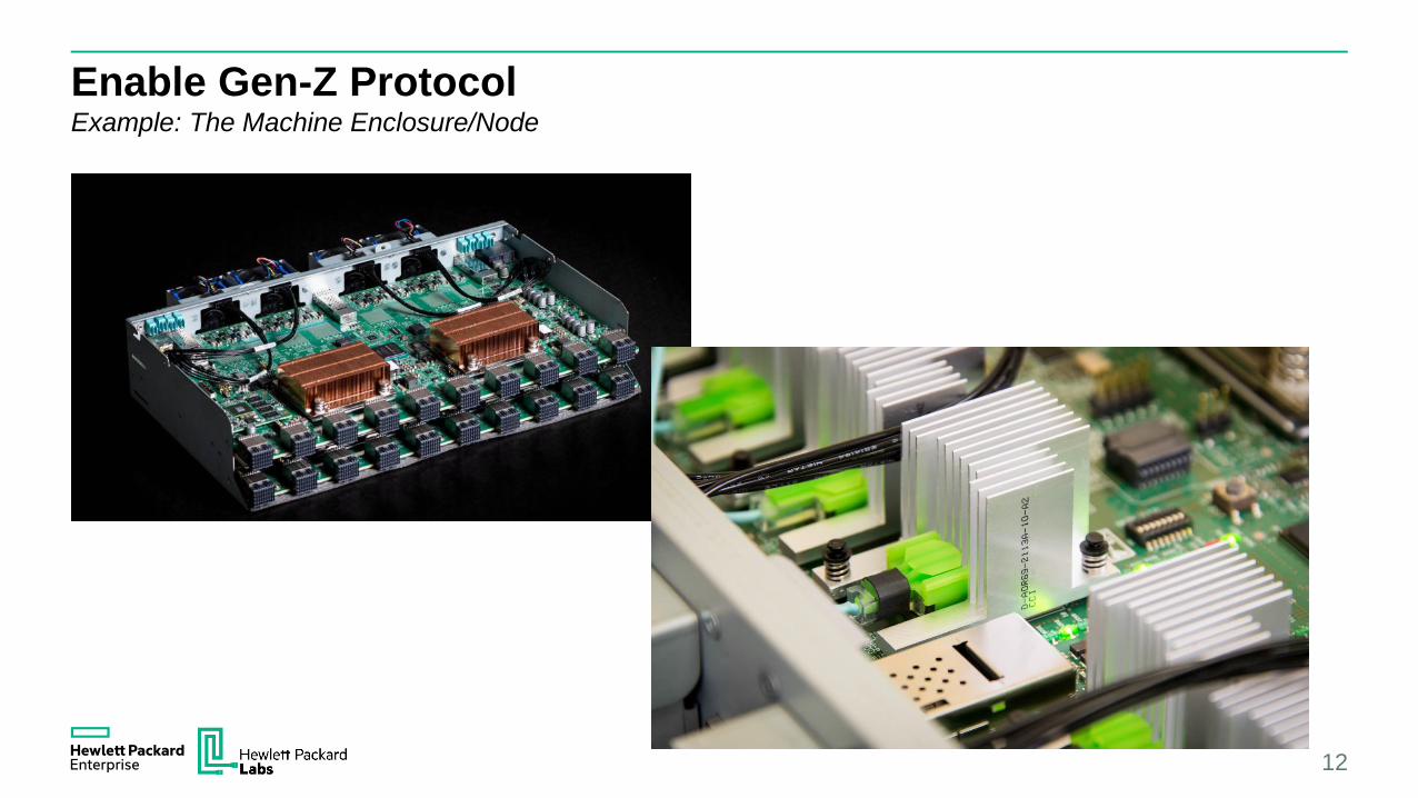
Enable Gen-Z ProtocolExample: The Machine Enclosure/Node
12
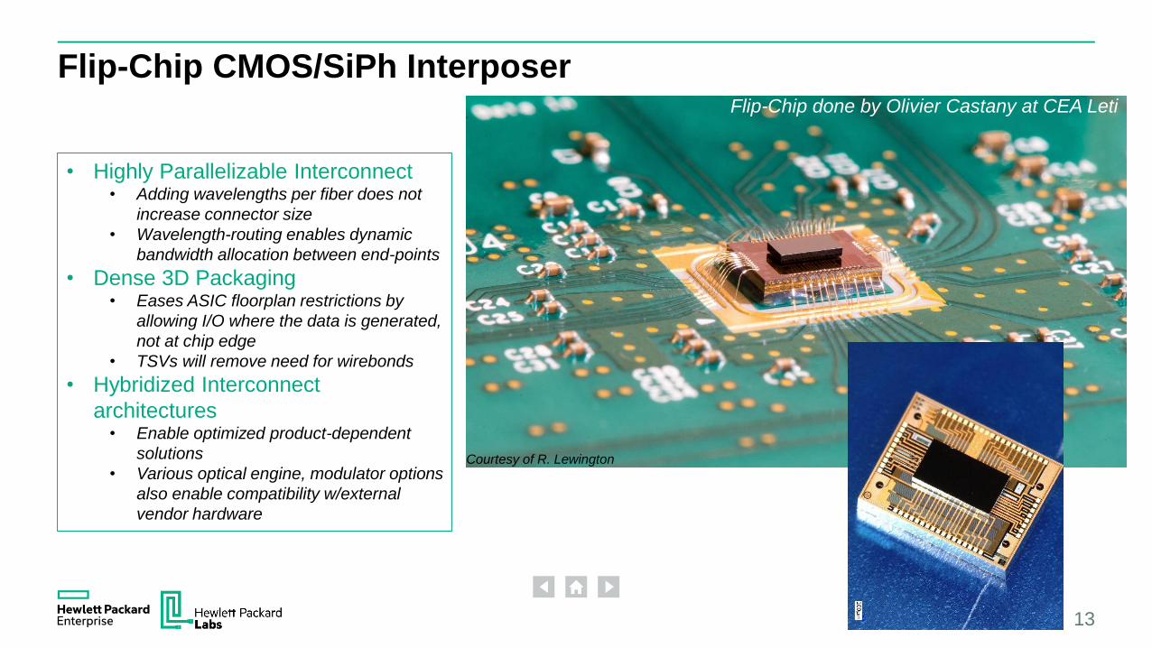
Flip-Chip CMOS/SiPh Interposer
13
• Highly Parallelizable Interconnect• Adding wavelengths per fiber does not
increase connector size
• Wavelength-routing enables dynamic
bandwidth allocation between end-points
• Dense 3D Packaging• Eases ASIC floorplan restrictions by
allowing I/O where the data is generated,
not at chip edge
• TSVs will remove need for wirebonds
• Hybridized Interconnect
architectures • Enable optimized product-dependent
solutions
• Various optical engine, modulator options
also enable compatibility w/external
vendor hardware
Courtesy of R. Lewington
Flip-Chip done by Olivier Castany at CEA Leti
HPE Confidential 14
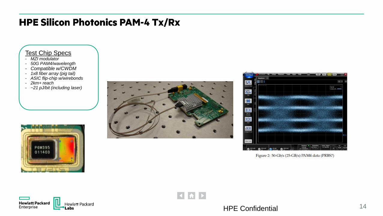
Test Chip Specs- MZI modulator- 50G PAM4/wavelength- Compatible w/CWDM- 1x8 fiber array (pig tail)- ASIC flip-chip w/wirebonds- 2km+ reach- ~21 pJ/bit (including laser)