Embed Size (px)
Citation preview

UIUC - CS 433IBM POWER7
Adam KunkAnil JohnPete Bohman

Quick Facts
Released by IBM in 2010 (~ February) Successor of the POWER6 Shift from high frequency to multi-core Implements IBM PowerPC architecture v2.06
Clock Rate: 2.4 GHz - 4.25 GHz Feature size: 45 nm ISA: Power ISA v 2.06 (RISC) Cores: 4, 6, 8 Cache: L1, L2, L3 – On Chip
References: [1], [5]

Why the POWER7?
PERCS – Productive, Easy-to-use, Reliable Computer System DARPA funded contract that IBM won in order
to develop the Power7 ($244 million contract, 2006)▪ Contract was to develop a petascale supercomputer
architecture before 2011 in the HPCS (High Performance Computing Systems) project.
IBM, Cray, and Sun Microsystems received HPCS grant for Phase II.
IBM was chosen for Phase III in 2006.
References: [1], [2]

Blue Waters
Side note: The Blue Waters system was meant to
be the first supercomputer using PERCS technology.
But, the contract was cancelled (cost and complexity).

History of Power
2004 2001 2007 2010
POWER4/4+
Dual Core Chip Multi Processing Distributed Switch Shared L2 Dynamic LPARs (32)180nm,
POWER5/5+
Dual Core & Quad Core MdEnhanced Scaling2 Thread SMTDistributed Switch +Core Parallelism +FP Performance +Memory bandwidth +130nm, 90nm
POWER6/6+
Dual Core High Frequencies Virtualization + Memory Subsystem + Altivec Instruction Retry Dyn Energy Mgmt 2 Thread SMT + Protection Keys 65nm
POWER7/7+
4,6,8 Core 32MB On-Chip eDRAM Power Optimized Cores Mem Subsystem ++ 4 Thread SMT++ Reliability + VSM & VSX Protection Keys+ 45nm, 32nm
POWER8
Future
First Dual Corein Industry
HardwareVirtualizationfor Unix & Linux
FastestProcessorIn Industry
MostPOWERful &ScalableProcessor inIndustry
References: [3]

POWER7 Layout
Cores: 8 Intelligent Cores / chip (socket) 4 and 6 Intelligent Cores available
on some models 12 execution units per core Out of order execution 4 Way SMT per core 32 threads per chip L1 – 32 KB I Cache / 32 KB D
Cache per core L2 – 256 KB per coreChip: 32MB Intelligent L3 Cache on chip
Core
L2
Core
L2
Memory Interface
Core
L2
Core
L2
Core
L2
Core
L2
Core
L2
Core
L2
GX
SMP
FABRIC
POWER
BUS
Memory++
L3 CacheeDRAM
References: [3]

POWER7 Options (8, 6, 4 cores)
References: [3]

POWER7 TurboCore
TurboCore mode 8 core to 4 Core 7.25% higher core frequency 2X the amount of L3 cache (fluid cache)
Tradeoffs Reduces per core software licenses Increases throughput computing Decreases parallel transactional based
workloads

POWER7 Core
Each core implements “aggressive” out-of-order (OoO) instruction execution
The processor has an Instruction Sequence Unit capable of dispatching up to six instructions per cycle to a set of queues
Up to eight instructions per cycle can be issued to the Instruction Execution units
References: [4]

Pipeline

Instruction Fetch
8 inst. fetched from L2 to L1 I-cache or fetch buffer Balanced instruction rates across active threads Inst. Grouping
Instructions belonging to group issued together Groups contain independent instructions

Branch Prediction
POWER7 uses different mechanisms to predict the branch direction (taken/not taken) and the branch target address.
Instruction Fetch Unit (IFU) supports 3-cycle branch scan loop (to scan instructions for branches taken, compute target addresses, and determine if it is an unconditional branch or taken)
References: [5]

Branch Direction Prediction Tournament Predictor (due to GSEL):
8-K entry local BHT (LBHT)▪ BHT – Branch History Table
16-K entry global BHT (GBHT) 8-K entry global selection array (GSEL)
All arrays above provide branch direction predictions for all instructions in a fetch group (fetch group - up to 8 instructions)
The arrays are shared by all threadsReferences: [5]
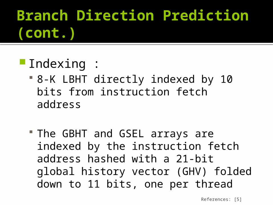
Branch Direction Prediction (cont.)
Indexing : 8-K LBHT directly indexed by 10 bits
from instruction fetch address
The GBHT and GSEL arrays are indexed by the instruction fetch address hashed with a 21-bit global history vector (GHV) folded down to 11 bits, one per thread
References: [5]

Branch Direction Prediction (cont.)
Value in GSEL chooses between LBHT and GBHT for the direction of the prediction of each individual branch Hence the tournament predictor!
Each BHT (LBHT and GBHT) entry contains 2 bits: Higher order bit determines direction
(taken/not taken) Lower order bit provides hysteresis (history of
the branch)References: [5]

Branch Target Address Prediction
Predicted in two ways:1. Indirect branches that are not
subroutine returns use a 128-entry count cache (shared by all active threads).
▪ Count cache is indexed by doing an XOR of 7 bits from the instruction fetch address and the GHV (global history vector)
▪ Each entry in the count cache contains a 62-bit predicted address with 2 confidence bits
References: [5]

Branch Target Address Prediction (cont.)
Predicted in two ways:1. Subroutine returns are predicted using
a link stack (one per thread). ▪ This is like the “Return Address Stack”
discussed in lecture
Support in POWER7 modes: ST, SMT2 16-entry link stack (per
thread) SMT4 8-entry link stack (per thread)

Execution Units
Each POWER7 core has 12 execution units: 2 fixed point units 2 load store units 4 double precision floating point units (2x
power6) 1 vector unit 1 branch unit 1 condition register unit 1 decimal floating point unit
References: [4]

ILP
Advanced branch prediction Large out of order execution
windows Large and fast caches Execute more than one execution
thread per core A single 8-core Power7 processor can
execute 32 threads in the same clock cycle.

POWER7 Demo
IBM POWER7 Demo
Visual representation of the SMT capabilities of the POWER7
Brief introduction to the on-chip L3 cache

SMT
Simultaneous Multithreading Separate instruction streams running
concurrently on the same physical processor
POWER7 supports: 2 pipes for storage instructions (load/stores) 2 pipes for executing arithmetic instructions
(add, subtract, etc.) 1 pipe for branch instructions (control flow) Parallel support for floating-point and vector
operationsReferences: [7], [8]

SMT (cont.)
Simultaneous Multithreading Explanation: SMT1: Single instruction execution thread per
core SMT2: Two instruction execution threads per core SMT4: Four instruction execution threads per
core
This means that an 8-core Power7 can execute 32 threads simultaneously
POWER7 supports SMT1, SMT2, SMT4References: [5], [8]

Multithreading History
Thread 1 Executing
Thread 0 Executing
No Thread Executing
FX0FX1FP0FP1LS0LS1BRXCRL
Single thread Out of Order
FX0FX1FP0FP1LS0LS1BRXCRL
S80 HW Multi-thread
FX0FX1FP0FP1LS0LS1BRXCRL
POWER5 2 Way SMT
FX0FX1FP0FP1LS0LS1BRXCRL
POWER7 4 Way SMT
Thread 3 Executing
Thread 2 ExecutingReferences: [3]

Cache Overview
Parameter L1 L2 L3 (Local) L3 (Global)
Size 64 KB (32K I, 32K D)
256 KB 4 MB 32 MB
Location Core Core On-Chip On-Chip
Access Time
.5 ns 2 ns 6 ns 30 ns
Associativity
4-way I-cache8-way D-cache
8-way 8-way 8-way
Write Policy
Write Through
Write Back Partial Victim
Adaptive
Line size 128 B 128 B 128 B 128 B

Cache Design Considerations
On-Chip cache required for sufficient bandwidth to 8 cores. Previous off-chip socket interface unable
to scale Support dynamic cores Utilize ILP and increased SMT latency
overlap

L1 Cache
I and D cache split to reduce latency Way prediction bits reduce hit
latency Write-Through
No L1 write-backs required on line eviction
High speed L2 able to handle bandwidth B-Tree LRU replacement Prefetching
On each L1 I-Cache miss, prefetch next 2 blocks

L2 Cache
Superset of L1 (inclusive) Reduced latency by decreasing capacity
L2 utilizes larger L3-Local cache as victim cache Increased associativity

L3 Cache
32 MB Fluid L3 cache Lateral cast outs, disabled core provisioning
4 MB of local L3 cache per 8 cores▪ Local cache closer to respective core, reduced latency
L3 cache access routed to the local L3 cache first Cache lines cloned when used by multiple cores

eDRAM
Embedded Dynamic Random-Access memory Less area (1 transistor vs. 6 transistor SRAM) Enables on-chip L3 cache
▪ Reduces L3 latency▪ Larger internal bus size which increases bandwidth
Compared to off chip SRAM cache▪ 1/6 latency▪ 1/5 standby power
Utilized in game consoles (PS2, Wii, Etc.)References: [5], [6]

Memory
2 memory controllers, 4 channels per core Exploits elimination of off-chip L3 cache
interface
32 GB per core, 256 GB Capacity 180 GB/s (Power6 75GB/s) 16 KB scheduling buffer

Maintaining The Balance

Energy Management
Three idle states to optimize power vs. latency
Nap Sleep “Heavy” Sleep

Energy Management
Nap Optimized for wake-up time Turn off clocks to execution units Caches remain coherent Reduce frequency to core

Energy Management
Sleep Purge and clock off core plus caches
“Heavy” Sleep Optimized for power reduction All cores sleep mode Reduce voltage of all cores Voltage ramps automatically on wake-up No hardware re-initialization required

Energy Management
Per-core frequency Scaling: -50% thru +10% frequency slew
independent per core. (DVFS) Supports energy optimization in
partitioned system configuration▪ Less utilized partitions can run at lower
frequencies▪ Heavily utilized partitions maintain peak
performance Each partition can run under different
energy saving policy

Energy Management Impact IBM research states the following
improvements in SPECPower_ssj2008 scores Adding dynamic fan speed control
▪ 14% improvement Static power savings (low power operation)
▪ 24% improvement Dynamic power savings (DVFS with Turbo
mode)▪ 50% improvement

Performance
Technology Chips Cores Threads GHz rPerf CPW
POWER7 2 16 64 3.86 195.45 105,200
POWER7 2 16 64 3.92 197.6 106,000
POWER7 2 8 32 4.14 115.86 57,450
rPerf – Relative performance metric for Power Systems servers.•Derived from an IBM analytical model which uses characteristics from IBM internal workloads, TPC and SPEC benchmarks.
•The IBM eServer pSeries 640 is the baseline reference system and has a value of 1.0.
CPW – Commercial Processing Workload •Based on benchmarks owned and managed by the Transaction Processing Performance Council.
•Provides an indicator of transaction processing performance capacity when comparing between members of the iSeries and AS/400 families.

Performance
Technology Chips Cores Threads GHz SPECint SPECfp
POWER7 2 16 16 3.86 71.5
POWER7 2 16 16 4.14 44.0
Technology Chips Cores Threads GHz OSSPECint
_rateSPECfp_
rate
POWER7 2 16 64 3.86 AIX 6.1 652 586
SPEC CPU2006 performance (Speed)
SPEC CPU2006 performance (Throughput)

References
1. http://en.wikipedia.org/wiki/POWER7 2. http://en.wikipedia.org/wiki/PERCS 3. Central PA PUG POWER7 review.ppt
http://www.google.com/url?sa=t&rct=j&q=&esrc=s&source=web&cd=1&ved=0CCEQFjAA&url=http%3A%2F%2Fwww.ibm.com%2Fdeveloperworks%2Fwikis%2Fdownload%2Fattachments%2F135430247%2FCentral%2BPA%2BPUG%2BPOWER7%2Breview.ppt&ei=3El3T6ejOI-40QGil-GnDQ&usg=AFQjCNFESXDZMpcC2z8y8NkjE-v3S_5t3A

References (cont.)
4. http://www.redbooks.ibm.com/redpapers/pdfs/redp4639.pdf
5. http://www.serc.iisc.ernet.in/~govind/243/Power7.pdf
6. http://en.wikipedia.org/wiki/EDRAM 7.
http://www.spscicomp.org/ScicomP16/presentations/Power7_Performance_Overview.pdf
8. http://www-03.ibm.com/systems/resources/pwrsysperf_SMT4OnP7.pdf