Embed Size (px)
Citation preview

JFET Input Instrumentation Amplifier with Rail-to-Rail Output in MSOP Package
AD8220
Rev. B Information furnished by Analog Devices is believed to be accurate and reliable. However, no responsibility is assumed by Analog Devices for its use, nor for any infringements of patents or other rights of third parties that may result from its use. Specifications subject to change without notice. No license is granted by implication or otherwise under any patent or patent rights of Analog Devices. Trademarks and registered trademarks are the property of their respective owners.
One Technology Way, P.O. Box 9106, Norwood, MA 02062-9106, U.S.A.Tel: 781.329.4700 www.analog.com Fax: 781.461.3113 ©2006–2010 Analog Devices, Inc. All rights reserved.
FEATURES Low input currents
10 pA maximum input bias current (B grade) 0.6 pA maximum input offset current (B grade)
High CMRR 100 dB CMRR (minimum), G = 10 (B grade) 80 dB CMRR (minimum) to 5 kHz, G = 1 (B grade)
Excellent ac specifications and low power 1.5 MHz bandwidth (G = 1) 14 nV/√Hz input noise (1 kHz) Slew rate: 2 V/μs 750 μA quiescent supply current (maximum)
Versatile MSOP package Rail-to-rail output Input voltage range to below negative supply rail 4 kV ESD protection 4.5 V to 36 V single supply ±2.25 V to ±18 V dual supply Gain set with single resistor (G = 1 to 1000)
Qualified for automotive applications
APPLICATIONS Medical instrumentation Precision data acquisition Transducer interfaces
PIN CONFIGURATION
TOP VIEW(Not to Scale)
035
79-0
05
–IN 1
RG 2
RG 3
+IN 4
+VS8
VOUT7
REF6
–VS5
AD8220
Figure 1.
10n
1n
100p
10p
1p
0.1p
–50 150
035
79-0
59
TEMPERATURE (°C)
INP
UT
BIA
S C
UR
RE
NT
(A
)
–25 0 25 50 75 100 125
IOS
IBIAS
Figure 2. Input Bias Current and Offset Current vs. Temperature
GENERAL DESCRIPTION The AD8220 is the first single-supply, JFET input instrumentation amplifier available in an MSOP package. Designed to meet the needs of high performance, portable instrumentation, the AD8220 has a minimum common-mode rejection ratio (CMRR) of 86 dB at dc and a minimum CMRR of 80 dB at 5 kHz for G = 1. Maxi-mum input bias current is 10 pA and typically remains below 300 pA over the entire industrial temperature range. Despite the JFET inputs, the AD8220 typically has a noise corner of only 10 Hz.
With the proliferation of mixed-signal processing, the number of power supplies required in each system has grown. The AD8220 is designed to alleviate this problem. The AD8220 can operate on a ±18 V dual supply, as well as on a single +5 V supply. Its rail-to-rail output stage maximizes dynamic range on the low voltage supplies common in portable applications. Its ability to run on a single 5 V supply eliminates the need to use higher voltage, dual supplies. The AD8220 draws a maximum of 750 μA of quiescent current, making it ideal for battery powered devices.
Gain is set from 1 to 1000 with a single resistor. Increasing the gain increases the common-mode rejection. Measurements that need higher CMRR when reading small signals benefit when the AD8220 is set for large gains.
A reference pin allows the user to offset the output voltage. This feature is useful when interfacing with analog-to-digital converters.
The AD8220 is available in an MSOP that takes roughly half the board area of an SOIC. Performance for the A and B grade is specified over the industrial temperature range of −40°C to +85°C, and the W grade is specified over the automotive temperature range of −40°C to +125°C.

AD8220
Rev. B | Page 2 of 28
TABLE OF CONTENTS Features .............................................................................................. 1
Applications ....................................................................................... 1
Pin Configuration ............................................................................. 1
General Description ......................................................................... 1
Revision History ............................................................................... 2
Specifications ..................................................................................... 3
Absolute Maximum Ratings ............................................................ 8
ESD Caution .................................................................................. 8
Pin Configuration and Function Descriptions ............................. 9
Typical Performance Characteristics ........................................... 10
Theory of Operation ...................................................................... 19
Gain Selection ............................................................................. 20
Layout ........................................................................................... 20
Reference Terminal .................................................................... 21
Power Supply Regulation and Bypassing ................................ 21
Input Bias Current Return Path ............................................... 21
Input Protection ......................................................................... 21
RF Interference ........................................................................... 22
Common-Mode Input Voltage Range ..................................... 22
Driving an ADC ......................................................................... 22
Applications Information .............................................................. 23
AC-Coupled Instrumentation Amplifier ................................ 23
Differential Output .................................................................... 23
Electrocardiogram Signal Conditioning ................................. 25
Outline Dimensions ....................................................................... 26
Ordering Guide .......................................................................... 26
Automotive Products ................................................................. 26
REVISION HISTORY 5/10—Rev. A to Rev. B Added W Grade .................................................................. Universal Changes to Features Section and General Description Section . 1 Changes to Specifications Section and Table 1 ............................. 3 Changes to Table 2 ............................................................................ 5 Updated Outline Dimensions ....................................................... 26 Changes to Ordering Guide .......................................................... 26 Added Automotive Products Section .......................................... 26
5/07—Rev. 0 to Rev. A Changes to Table 1 ............................................................................. 3 Changes to Table 2 ............................................................................. 5 Changes to Table 3 ............................................................................. 8 Changes to Figure 6 and Figure 7 ................................................. 10 Changes to Figure 23 and Figure 24............................................. 13 Changes to Theory of Operation .................................................. 19 Changes to Layout .......................................................................... 20 Changes to Ordering Guide .......................................................... 26 4/06—Revision 0: Initial Version

AD8220
Rev. B | Page 3 of 28
SPECIFICATIONS VS+ = 15 V, VS− = −15 V, VREF = 0 V, TA = 25°C, TOPR = −40°C to +85°C for A and B grades. TOPR = −40°C to +125°C for W grade, G = 1, RL = 2 kΩ1, unless otherwise noted.
Table 1. A Grade B Grade W Grade Parameter Test Conditions Min Typ Max Min Typ Max Min Typ Max Unit COMMON-MODE
REJECTION RATIO (CMRR) TA for A, B grades, TOPR for W grade
CMRR DC to 60 Hz with 1 kΩ Source Imbalance
VCM = ±10 V
G = 1 78 86 77 dB G = 10 94 100 92 dB G = 100 94 100 92 dB G = 1000 94 100 92 dB
CMRR at 5 kHz VCM = ±10 V G = 1 74 80 72 dB G = 10 84 90 80 dB G = 100 84 90 80 dB G = 1000 84 90 80 dB
NOISE RTI noise = √(eni
2 + (eno/G)2), TA
Voltage Noise, 1 kHz Input Voltage Noise, eni VIN+, VIN− = 0 V 14 14 17 14 nV/√Hz Output Voltage Noise, eno VIN+, VIN− = 0 V 90 90 100 90 nV/√Hz RTI, 0.1 Hz to 10 Hz
G = 1 5 5 5 μV p-p G = 1000 0.8 0.8 0.8 μV p-p
Current Noise f = 1 kHz 1 1 1 fA/√Hz
VOLTAGE OFFSET VOS = VOSI + VOSO/G Input Offset, VOSI TA −250 +250 −125 +125 −250 +250 μV
Average TC TOPR −10 +10 −5 +5 −10 +10 μV/°C Output Offset, VOSO TA −750 +750 −500 +500 −750 +750 μV
Average TC TOPR −10 +10 −5 +5 −10 +10 μV/°C Offset RTI vs. Supply
(PSR) VS = ±5 V to ±15 V, TA for A, B grades, TOPR for W grade
G = 1 86 86 80 dB G = 10 96 100 92 dB G = 100 96 100 92 dB G = 1000 96 100 92 dB
INPUT CURRENT Input Bias Current TA 25 10 25 pA
Over Temperature TOPR 0.3 0.3 100 nA Input Offset Current TA 2 0.6 2 pA
Over Temperature TOPR 0.005 0.005 10 nA
DYNAMIC RESPONSE Small Signal Bandwidth,
−3 dB TA
G = 1 1500 1500 1500 kHz G = 10 800 800 800 kHz G = 100 120 120 120 kHz G = 1000 14 14 14 kHz

AD8220
Rev. B | Page 4 of 28
A Grade B Grade W Grade Parameter Test Conditions Min Typ Max Min Typ Max Min Typ Max Unit
Settling Time 0.01% 10 V step, TA G = 1 5 5 5 μs G = 10 4.3 4.3 4.3 μs G = 100 8.1 8.1 8.1 μs G = 1000 58 58 58 μs
Settling Time 0.001% 10 V step, TA G = 1 6 6 6 μs G = 10 4.6 4.6 4.6 μs G = 100 9.6 9.6 9.6 μs G = 1000 74 74 74 μs
Slew Rate G = 1 to 100 TA 2 2 2 V/μs
GAIN G = 1 + (49.4 kΩ/RG), TA for A, B grades, TOPR for W grade
Gain Range 1 1000 1 1000 1 1000 V/V Gain Error VOUT = ±10 V
G = 1 −0.06 +0.06 −0.04 +0.04 −0.1 +0.1 % G = 10 −0.3 +0.3 −0.2 +0.2 −0.8 +0.8 % G = 100 −0.3 +0.3 −0.2 +0.2 −0.8 +0.8 % G = 1000 −0.3 +0.3 −0.2 +0.2 −0.8 +0.8 %
Gain Nonlinearity VOUT = −10 V to +10 V, TA
G = 1 RL = 10 kΩ 10 15 10 15 10 15 ppm G = 10 RL = 10 kΩ 5 10 5 10 5 10 ppm G = 100 RL = 10 kΩ 30 60 30 60 30 60 ppm G = 1000 RL = 10 kΩ 400 500 400 500 400 500 ppm G = 1 RL = 2 kΩ 10 15 10 15 10 15 ppm G = 10 RL = 2 kΩ 10 15 10 15 10 15 ppm G = 100 RL = 2 kΩ 50 75 50 75 50 75 ppm
Gain vs. Temperature G = 1 3 10 2 5 3 10 ppm/°C G > 10 −50 −50 −50 ppm/°C
INPUT Impedance (Pin to
Ground)2 TA 104||5 104||5 104||5 GΩ||pF
Input Operating Voltage Range3
VS = ±2.25 V to ±18 V for dual supplies
−VS − 0.1
+VS − 2
−VS − 0.1
+VS − 2
−VS − 0.1
+VS − 2 V
Over Temperature TOPR −VS − 0.1
+VS − 2.1
−VS − 0.1
+VS − 2.1
−VS − 0.1
+VS − 2.2
V
OUTPUT Output Swing RL = 10 kΩ, TA −14.7 +14.7 −14.7 +14.7 −14.7 +14.7 V
Over Temperature TOPR −14.6 +14.6 −14.6 +14.6 −14.3 +14.3 V Short-Circuit Current TA 15 15 15 mA
REFERENCE INPUT TA kΩ RIN 40 40 40 μA IIN VIN+, VIN− = 0 V 70 70 70 V Voltage Range −VS +VS −VS +VS +VS V/V Gain to Output TA 1 ±
0.0001 1 ±
0.0001 1 ±
0.0001 V/V

AD8220
Rev. B | Page 5 of 28
A Grade B Grade W Grade Parameter Test Conditions Min Typ Max Min Typ Max Min Typ Max Unit POWER SUPPLY V
Operating Range ±2.254 ±18 ±2.254 ±18 ±2.254 ±18 μA
Quiescent Current TA 750 750 750 μA Over Temperature TOPR 850 850 1000 μA
TEMPERATURE RANGE For Specified
Performance TOPR −40 +85 −40 +85 −40 +125 °C
1 When the output sinks more than 4 mA, use a 47 pF capacitor in parallel with the load to prevent ringing. Otherwise, use a larger load, such as 10 kΩ. 2 Differential and common-mode input impedance can be calculated from the pin impedance: ZDIFF = 2(ZPIN); ZCM = ZPIN/2. 3 The AD8220 can operate up to a diode drop below the negative supply but the bias current increases sharply. The input voltage range reflects the maximum
allowable voltage where the input bias current is within the specification. 4 At this supply voltage, ensure that the input common-mode voltage is within the input voltage range specification.
VS + = 5 V, VS− = 0 V, VREF = 2.5 V, TA = 25°C, TOPR = −40°C to +85°C for A and B grades. TOPR = −40°C to +125°C for W grade, G = 1, RL = 2 kΩ1, unless otherwise noted.
Table 2. A Grade B Grade W Grade Parameter Test Conditions Min Typ Max Min Typ Max Min Typ Max Unit COMMON-MODE REJECTION
RATIO (CMRR) TA for A, B grades, TOPR for W grade
CMRR DC to 60 Hz with 1 kΩ Source Imbalance
VCM = 0 to 2.5 V
G = 1 78 86 77 dB G = 10 94 100 92 dB G = 100 94 100 92 dB G = 1000 94 100 92 dB
CMRR at 5 kHz VCM = 0 to 2.5 V G = 1 74 80 72 dB G = 10 84 90 80 dB G = 100 84 90 80 dB G = 1000 84 90 80 dB
NOISE RTI noise = √(eni2 +
(eno/G)2), TA
Voltage Noise, 1 kHz VS = ±2.5 V Input Voltage Noise, eni VIN+, VIN− = 0 V, VREF =
0 V 14 14 17 14 nV/√Hz
Output Voltage Noise, eno VIN+, VIN− = 0 V, VREF = 0 V
90 90 100 90 nV/√Hz
RTI, 0.1 Hz to 10 Hz G = 1 5 5 5 μV p-p G = 1000 0.8 0.8 0.8 μV p-p
Current Noise f = 1 kHz 1 1 1 fA/√Hz
VOLTAGE OFFSET VOS = VOSI + VOSO/G Input Offset, VOSI TA −300 +300 −200 +200 −300 +300 μV
Average TC TOPR −10 +10 −5 +5 −10 10 μV/°C Output Offset, VOSO TA −800 +800 −600 +600 −800 +800 μV
Average TC TOPR −10 +10 −5 +5 −10 +10 μV/°C Offset RTI vs. Supply (PSR) TA for A, B grades,
TOPR for W grade
G = 1 86 86 80 dB G = 10 96 100 92 dB G = 100 96 100 92 dB G = 1000 96 100 92 dB

AD8220
Rev. B | Page 6 of 28
A Grade B Grade W Grade Parameter Test Conditions Min Typ Max Min Typ Max Min Typ Max Unit INPUT CURRENT
Input Bias Current TA 25 10 25 pA Over Temperature TOPR 0.3 0.3 100 nA
Input Offset Current TA 2 0.6 2 pA Over Temperature TOPR 0.005 0.005 10 nA
DYNAMIC RESPONSE TA Small Signal Bandwidth,
−3 dB
G = 1 1500 1500 1500 kHz G = 10 800 800 800 kHz G = 100 120 120 120 kHz G = 1000 14 14 14 kHz
Settling Time 0.01% TA G = 1 3 V step 2.5 2.5 2.5 μs G = 10 4 V step 2.5 2.5 2.5 μs G = 100 4 V step 7.5 7.5 7.5 μs G = 1000 4 V step 30 30 30 μs
Settling Time 0.001% TA G = 1 3 V step 3.5 3.5 3.5 μs G = 10 4 V step 3.5 3.5 3.5 μs G = 100 4 V step 8.5 8.5 8.5 μs G = 1000 4 V step 37 37 37 μs
Slew Rate G = 1 to 100 TA 2 2 2 V/μs
GAIN G = 1 + (49.4 kΩ/RG), TA for A, B grades, TOPR for W grade
Gain Range 1 1000 1 1000 1 1000 V/V Gain Error VOUT = 0.3 V to 2.9 V for
G = 1, VOUT = 0.3 V to 3.8 V for G > 1
G = 1 −0.06 +0.06 −0.04 +0.04 −0.1 +0.1 % G = 10 −0.3 +0.3 −0.2 +0.2 −0.8 +0.8 % G = 100 −0.3 +0.3 −0.2 +0.2 −0.8 +0.8 % G = 1000 −0.3 +0.3 −0.2 +0.2 −0.8 +0.8 %
Nonlinearity VOUT = 0.3 V to 2.9 V for G = 1, VOUT = 0.3 V to 3.8 V for G > 1, TA
G = 1 RL = 10 kΩ 35 50 35 50 50 ppm G = 10 RL = 10 kΩ 35 50 35 50 50 ppm G = 100 RL = 10 kΩ 50 75 50 75 75 ppm G = 1000 RL = 10 kΩ 650 750 650 750 750 ppm G = 1 RL = 2 kΩ 35 50 35 50 50 ppm G = 10 RL = 2 kΩ 35 50 35 50 50 ppm G = 100 RL = 2 kΩ 50 75 50 75 75 ppm
Gain vs. Temperature G = 1 3 10 2 5 3 10 ppm/°C G > 10 −50 −50 −50 ppm/°C
INPUT Impedance (Pin to
Ground)2 TA 104||6 104||6 104||6 GΩ||pF
Input Voltage Range3 TA −0.1 +VS − 2
−0.1 +VS − 2
V
Over Temperature TOPR −0.1 +VS − 2.1
−0.1 +VS − 2.1
−0.1 +VS − 2.2
V

AD8220
Rev. B | Page 7 of 28
A Grade B Grade W Grade Parameter Test Conditions Min Typ Max Min Typ Max Min Typ Max Unit OUTPUT
Output Swing RL = 10 kΩ 0.15 4.85 0.15 4.85 0.15 4.85 V Over Temperature TOPR 0.2 4.80 0.2 4.80 0.3 4.70 V
Short-Circuit Current 15 15 15 mA
REFERENCE INPUT TA RIN 40 40 40 kΩ IIN VIN+, VIN− = 0 V 70 70 70 μA Voltage Range −VS +VS −VS +VS −VS +VS V Gain to Output TA 1 ±
0.0001 1 ±
0.0001 1 ±
0.0001 V/V
POWER SUPPLY Operating Range 4.5 36 4.5 36 4.5 36 V Quiescent Current TA 750 750 750 μA
Over Temperature TOPR 850 850 1000 μA
TEMPERATURE RANGE TOPR, For Specified
Performance TOPR −40 +85 −40 +85 −40 +125 °C
1 When the output sinks more than 4 mA, use a 47 pF capacitor in parallel with the load to prevent ringing. Otherwise, use a larger load, such as 10 kΩ. 2 Differential and common-mode impedance can be calculated from the pin impedance: ZDIFF = 2(ZPIN); ZCM = ZPIN/2. 3 The AD8220 can operate up to a diode drop below the negative supply but the bias current increases sharply. The input voltage range reflects the maximum
allowable voltage where the input bias current is within the specification.

AD8220
Rev. B | Page 8 of 28
ABSOLUTE MAXIMUM RATINGS
Table 3. Parameter Rating Supply Voltage ±18 V Power Dissipation See Figure 3 Output Short-Circuit Current Indefinite1 Input Voltage (Common Mode) ±Vs Differential Input Voltage ±Vs Storage Temperature Range −65°C to +125°C Operating Temperature Range2 −40°C to +125°C Lead Temperature (Soldering 10 sec) 300°C Junction Temperature 140°C θJA (4-Layer JEDEC Standard Board) 135°C/W Package Glass Transition Temperature 140°C ESD (Human Body Model) 4 kV ESD (Charge Device Model) 1 kV ESD (Machine Model) 0.4 kV 1 Assumes the load is referenced to midsupply. 2 Temperature for specified performance is −40°C to +85°C. For performance
to 125°C, see the Typical Performance Characteristics section.
Stresses above those listed under Absolute Maximum Ratings may cause permanent damage to the device. This is a stress rating only; functional operation of the device at these or any other conditions above those indicated in the operational section of this specification is not implied. Exposure to absolute maximum rating conditions for extended periods may affect device reliability.
Figure 3 shows the maximum safe power dissipation in the package vs. the ambient temperature for the MSOP on a 4-layer JEDEC standard board. θJA values are approximations.
2.00
0–40 120
035
79-
045
AMBIENT TEMPERATURE (°C)
MA
XIM
UM
PO
WE
R D
ISS
IPA
TIO
N (
W) 1.75
1.50
1.25
1.00
0.75
0.50
0.25
–20 0 20 40 60 80 100
Figure 3. Maximum Power Dissipation vs. Ambient Temperature
ESD CAUTION

AD8220
Rev. B | Page 9 of 28
PIN CONFIGURATION AND FUNCTION DESCRIPTIONS
TOP VIEW(Not to Scale)
035
79-0
05
–IN 1
RG 2
RG 3
+IN 4
+VS8
VOUT7
REF6
–VS5
AD8220
Figure 4. Pin Configuration
Table 4. Pin Function Descriptions Pin No. Mnemonic Description 1 −IN Negative Input Terminal (True Differential Input) 2, 3 RG Gain Setting Terminals (Place Resistor Across the RG Pins) 4 +IN Positive Input Terminal (True Differential Input) 5 −VS Negative Power Supply Terminal 6 REF Reference Voltage Terminal (Drive This Terminal with a Low Impedance Voltage Source to Level-Shift the Output) 7 VOUT Output Terminal 8 +VS Positive Power Supply Terminal
AD8220
Rev. B | Page 10 of 28
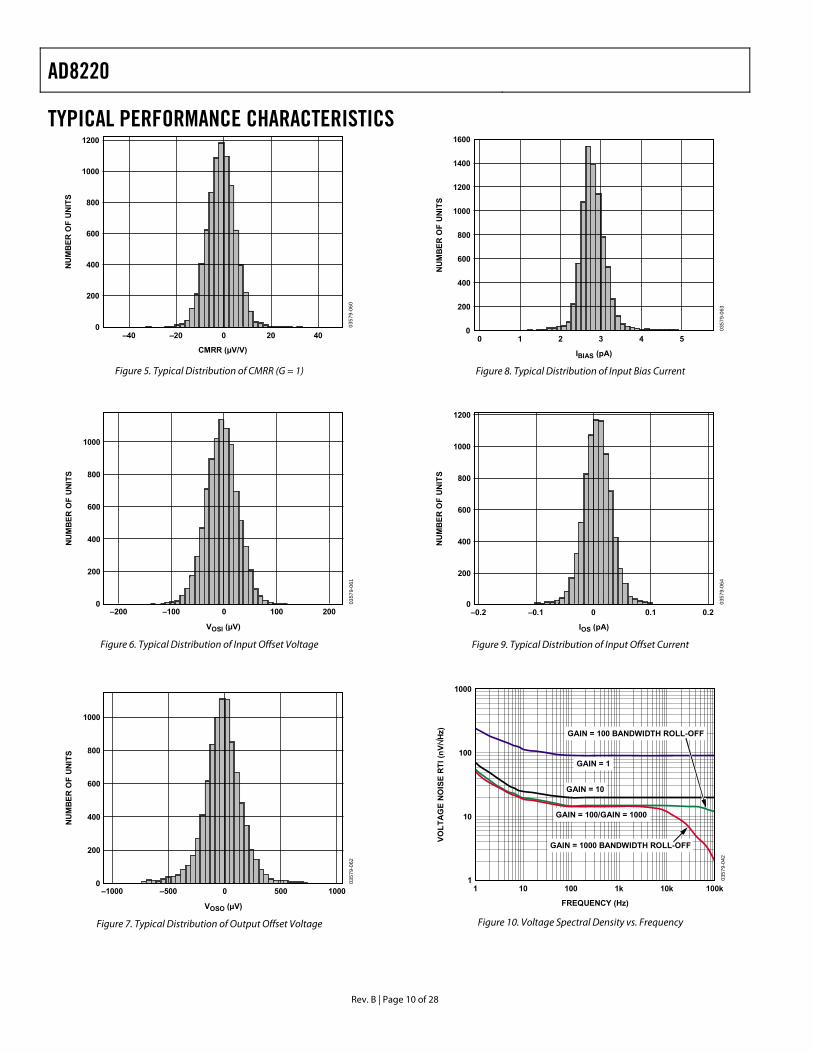
TYPICAL PERFORMANCE CHARACTERISTICS
0 035
79-0
60
CMRR (µV/V)
NU
MB
ER
OF
UN
ITS
1200
1000
800
600
400
200
–40 –20 0 20 40
Figure 5. Typical Distribution of CMRR (G = 1)
0 0357
9-0
61
VOSI (µV)
NU
MB
ER
OF
UN
ITS
1000
800
600
400
200
–200 –100 0 100 200
Figure 6. Typical Distribution of Input Offset Voltage
0 0357
9-0
62
VOSO (µV)
NU
MB
ER
OF
UN
ITS
1000
800
600
400
200
–1000 –500 0 500 1000
Figure 7. Typical Distribution of Output Offset Voltage
0 0357
9-0
63
IBIAS (pA)
NU
MB
ER
OF
UN
ITS
1600
1400
1200
1000
800
600
400
200
0 1 2 3 4 5
Figure 8. Typical Distribution of Input Bias Current
0 0357
9-0
64
IOS (pA)
NU
MB
ER
OF
UN
ITS
1200
1000
800
600
400
200
–0.2 –0.1 0 0.1 0.2
Figure 9. Typical Distribution of Input Offset Current
1000
11 100k
035
79-
042
FREQUENCY (Hz)
VO
LT
AG
E N
OIS
E R
TI
(nV
/H
z)
10 100 1k 10k
10
100
GAIN = 100 BANDWIDTH ROLL-OFF
GAIN = 1
GAIN = 10
GAIN = 100/GAIN = 1000
GAIN = 1000 BANDWIDTH ROLL-OFF
Figure 10. Voltage Spectral Density vs. Frequency
AD8220
Rev. B | Page 11 of 28
XX
XXXX XX
035
79-
024
XXX (X)
XX
X (
X)
1s/DIV5µV/DIV
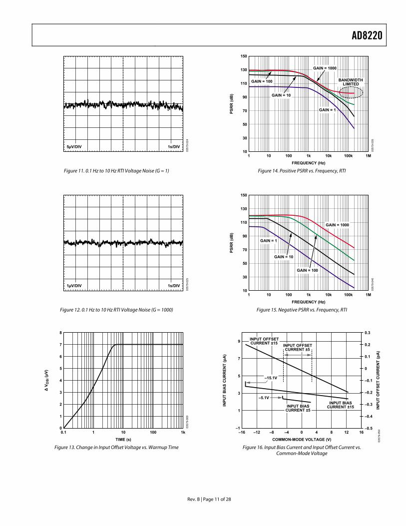
Figure 11. 0.1 Hz to 10 Hz RTI Voltage Noise (G = 1)
XX
XXXX XX
035
79-
025
XXX (X)
XX
X (
X)
1s/DIV1µV/DIV
Figure 12. 0.1 Hz to 10 Hz RTI Voltage Noise (G = 1000)
8
00.1 1k
035
79-
009
TIME (s)
Δ V
OS
I (µ
V)
1 10 100
7
6
5
4
3
2
1
Figure 13. Change in Input Offset Voltage vs. Warmup Time
150
101 1M
035
79-
035
FREQUENCY (Hz)
PS
RR
(d
B)
10 100 1k 10k 100k
130
110
90
70
50
30
BANDWIDTHLIMITED
GAIN = 1
GAIN = 10
GAIN = 100
GAIN = 1000
Figure 14. Positive PSRR vs. Frequency, RTI
150
101 1M
035
79-
040
FREQUENCY (Hz)
PS
RR
(d
B)
10 100 1k 10k 100k
130
110
90
70
50
30
GAIN = 1
GAIN = 10
GAIN = 100
GAIN = 1000
Figure 15. Negative PSRR vs. Frequency, RTI
–1
1
3
5
7
9
–16 16
0357
9-05
0
COMMON-MODE VOLTAGE (V)
INP
UT
BIA
S C
UR
RE
NT
(p
A)
INP
UT
OF
FS
ET
CU
RR
EN
T (
pA
)
–12 –8 –4 0 4 8 12–0.5
–0.4
–0.3
–0.2
–0.1
0
0.1
0.2
0.3
INPUT OFFSETCURRENT ±5
–15.1V
–5.1V
INPUT OFFSETCURRENT ±15
INPUT BIASCURRENT ±15INPUT BIAS
CURRENT ±5
Figure 16. Input Bias Current and Input Offset Current vs. Common-Mode Voltage

AD8220
Rev. B | Page 12 of 28
10n
1n
100p
10p
1p
0.1p
–50 150
035
79-0
59
TEMPERATURE (°C)
INP
UT
BIA
S C
UR
RE
NT
(A
)
–25 0 25 50 75 100 125
IOS
IBIAS
Figure 17. Input Bias Current and Offset Current vs. Temperature, VS = ±15 V, VREF = 0 V
10n
1n
100p
10p
1p
0.1p
–50 150
035
79-0
65
TEMPERATURE (°C)
CU
RR
EN
T (
A)
–25 0 25 50 75 100 125
IOS
IBIAS
Figure 18. Input Bias Current and Offset Current vs. Temperature, VS = +5 V, VREF = 2.5 V
160
4010 100k
035
79-
023
FREQUENCY (Hz)
CM
RR
(d
B)
100 1k 10k
140
120
100
80
60
GAIN = 1
GAIN = 10
GAIN = 100
GAIN = 1000
BANDWIDTHLIMITED
Figure 19. CMRR vs. Frequency
160
401 100k
035
79-
051
FREQUENCY (Hz)
CM
RR
(d
B)
140
120
100
80
60
GAIN = 1GAIN = 10
GAIN = 1000
BANDWIDTHLIMITED
GAIN = 100
10 100 1k 10k
Figure 20. CMRR vs. Frequency, 1 kΩ Source Imbalance
10
–10–50 130
035
79-
034
TEMPERATURE (°C)
Δ C
MR
R (μ
V/V
)
8
6
4
2
0
–2
–4
–6
–8
–30 –10 10 30 50 70 90 110
Figure 21. Change in CMRR vs. Temperature, G = 1
70
–40100 10M
035
79-
022
FREQUENCY (Hz)
GA
IN (
dB
)
1k 10k 100k 1M
60
50
40
30
20
10
0
–10
–20
–30
GAIN = 1
GAIN = 10
GAIN = 100
GAIN = 1000
Figure 22. Gain vs. Frequency

AD8220
Rev. B | Page 13 of 28
035
79-0
26
OUTPUT VOLTAGE (V)
XX
X
NO
NL
INE
AR
ITY
(5p
pm
/DIV
)
–8–10 –6 –4 –2 0 2 4 6 8 10
RLOAD = 2kΩ
RLOAD = 10kΩ
VS = ±15V
Figure 23. Gain Nonlinearity, G = 1
035
79-0
27
OUTPUT VOLTAGE (V)
XX
X
NO
NL
INE
AR
ITY
(5p
pm
/DIV
)
–8–10 –6 –4 –2 0 2 4 6 8 10
RLOAD = 2kΩ
RLOAD = 10kΩ
VS = ±15V
Figure 24. Gain Nonlinearity, G = 10
035
79-0
28
OUTPUT VOLTAGE (V)
XX
X
NO
NL
INE
AR
ITY
(50
pp
m/D
IV)
–8–10 –6 –4 –2 0 2 4 6 8 10
RLOAD = 2kΩ
RLOAD = 10kΩ
VS = ±15V
Figure 25. Gain Nonlinearity, G = 100
035
79-0
29
OUTPUT VOLTAGE (V)
XX
X
NO
NL
INE
AR
ITY
(50
0pp
m/D
IV)
–8–10 –6 –4 –2 0 2 4 6 8 10
RLOAD = 2kΩ
RLOAD = 10kΩ
VS = ±15V
Figure 26. Gain Nonlinearity, G = 1000
18
–18–16 16
035
79-
037
OUTPUT VOLTAGE (V)
INP
UT
CO
MM
ON
-MO
DE
VO
LT
AG
E (
V)
12
6
0
–6
–12
–12 –8 –4 0 4 8 12
–15.3V
+13V
±15V SUPPLIES
±5V SUPPLIES
+14.9V, –8.3V
+14.9V, +5.5V
+4.95V, –3.3V
+4.95V, +0.6V
–14.8V, +5.5V
–14.8V, –8.3V
–4.8V, –3.3V
–4.8V, +0.6V
–5.3V
+3V
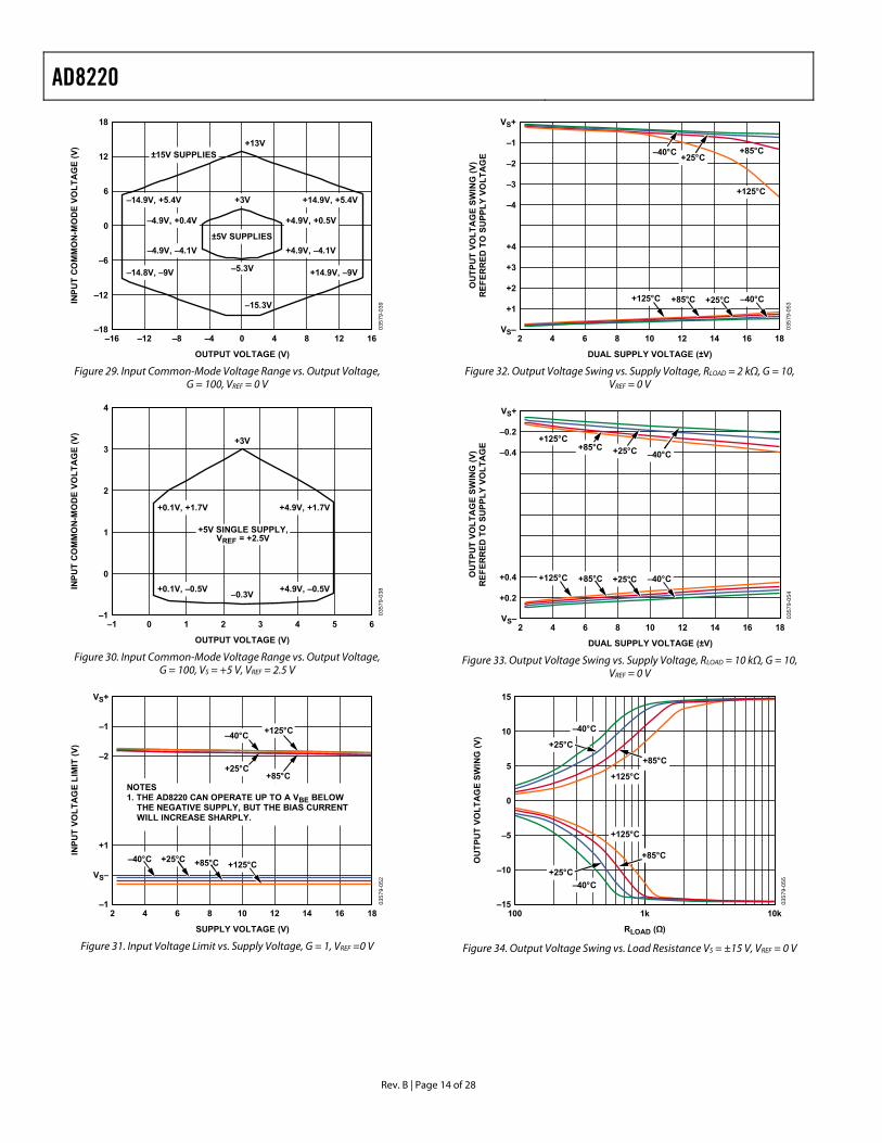
Figure 27. Input Common-Mode Voltage Range vs. Output Voltage, G = 1, VREF = 0 V
0 1 2 3 4 5
4
–1–1 6
035
79-
036
OUTPUT VOLTAGE (V)
INP
UT
CO
MM
ON
-MO
DE
VO
LT
AG
E (
V)
3
2
1
0
–0.3V
+3V
+4.9V, +0.5V
+4.9V, +1.7V
+5V SINGLE SUPPLY,VREF = +2.5V
+0.1V, +0.5V
+0.1V, +1.7V
Figure 28. Input Common-Mode Voltage Range vs. Output Voltage, G = 1, VS = +5 V, VREF = 2.5 V
AD8220
Rev. B | Page 14 of 28
18
–18–16 16
035
79-
039
OUTPUT VOLTAGE (V)
INP
UT
CO
MM
ON
-MO
DE
VO
LT
AG
E (
V)
12
6
0
–6
–12
–12 –8 –4 0 4 8 12
+13V
–15.3V
±15V SUPPLIES
+14.9V, –9V
+14.9V, +5.4V
+4.9V, +0.5V
+4.9V, –4.1V
–4.9V, +0.4V
–4.9V, –4.1V
–5.3V
+3V
–14.8V, –9V
–14.9V, +5.4V
±5V SUPPLIES
Figure 29. Input Common-Mode Voltage Range vs. Output Voltage, G = 100, VREF = 0 V
0 1 2 3 4 5
4
–1–1 6
035
79-
038
OUTPUT VOLTAGE (V)
INP
UT
CO
MM
ON
-MO
DE
VO
LT
AG
E (
V)
3
2
1
0
+3V
–0.3V
+4.9V, +1.7V
+4.9V, –0.5V
+0.1V, +1.7V
+0.1V, –0.5V
+5V SINGLE SUPPLY,VREF = +2.5V
Figure 30. Input Common-Mode Voltage Range vs. Output Voltage, G = 100, VS = +5 V, VREF = 2.5 V
VS+
–12 18
035
79-
052
SUPPLY VOLTAGE (V)
INP
UT
VO
LT
AG
E L
IMIT
(V
)
–1
–2
+1
VS–
4 6 8 10 12 14 16
–40°C+125°C
+25°C+85°C
+25°C–40°C
NOTES1. THE AD8220 CAN OPERATE UP TO A VBE BELOW THE NEGATIVE SUPPLY, BUT THE BIAS CURRENT WILL INCREASE SHARPLY.
+85°C +125°C
Figure 31. Input Voltage Limit vs. Supply Voltage, G = 1, VREF =0 V
VS+
VS–2 18
035
79-
053
DUAL SUPPLY VOLTAGE (±V)
OU
TP
UT
VO
LT
AG
E S
WIN
G (
V)
RE
FE
RR
ED
TO
SU
PP
LY
VO
LT
AG
E
–1
–2
–3
–4
+4
+3
+2
+1
4 6 8 10 12 14 16
–40°C+25°C
+125°C
+85°C
–40°C+25°C+85°C+125°C
Figure 32. Output Voltage Swing vs. Supply Voltage, RLOAD = 2 kΩ, G = 10, VREF = 0 V
VS+
VS–2 18
035
79-
054
DUAL SUPPLY VOLTAGE (±V)
OU
TP
UT
VO
LT
AG
E S
WIN
G (
V)
RE
FE
RR
ED
TO
SU
PP
LY
VO
LT
AG
E
–0.2
–0.4
+0.4
+0.2
4 6 8 10 12 14 16
+85°C+125°C +25°C –40°C
–40°C+25°C+85°C+125°C
Figure 33. Output Voltage Swing vs. Supply Voltage, RLOAD = 10 kΩ, G = 10, VREF = 0 V
15
–15100 10k
0357
9-0
55
RLOAD (Ω)
OU
TP
UT
VO
LT
AG
E S
WIN
G (
V)
1k
10
5
0
–5
–10
+125°C
+85°C
+25°C
–40°C
+125°C
+85°C
+25°C
–40°C
Figure 34. Output Voltage Swing vs. Load Resistance VS = ±15 V, VREF = 0 V

AD8220
Rev. B | Page 15 of 28
5
0100 10k
0357
9-0
56
RLOAD (Ω)
OU
TP
UT
VO
LT
AG
E S
WIN
G (
V)
1k
4
3
2
1
–40°C
–40°C
+125°C
+125°C
+25°C
+25°C
+85°C
+85°C
Figure 35. Output Voltage Swing vs. Load Resistance VS = +5 V, VREF = 2.5 V
VS+
VS–0 16
0357
9-0
57
IOUT (mA)
OU
TP
UT
VO
LT
AG
E S
WIN
G (
V)
RE
FE
RR
ED
TO
SU
PP
LY
VO
LT
AG
ES
–1
–2
–3
–4
+4
+3
+2
+1
2 4 6 8 10 12 14
–40°C
+125°C +85°C+25°C
–40°C
+25°C+85°C+125°C
Figure 36. Output Voltage Swing vs. Output Current, VS = ±15 V, VREF = 0 V
VS+
VS–0 16
0357
9-0
58
IOUT (mA)
OU
TP
UT
VO
LT
AG
E S
WIN
G (
V)
RE
FE
RR
ED
TO
SU
PP
LY
VO
LT
AG
ES
–1
–2
+2
+1
2 4 6 8 10 12 14
–40°C
+125°C+85°C
+25°C
+125°C
+25°C+85°C
Figure 37. Output Voltage Swing vs. Output Current, VS = 5 V, VREF = 2.5 V
XX
XXXX XX
035
79-
018
XXX (X)
XX
X (
X)
5µs/DIV20mV/DIV
100pF47pF
NO LOAD
Figure 38. Small Signal Pulse Response for Various Capacitive Loads, VS = ±15 V, VREF = 0 V
XX
XXXX XX
035
79-
019
XXX (X)
XX
X (
X)
5µs/DIV20mV/DIV
100pF
47pF
NO LOAD
Figure 39. Small Signal Pulse Response for Various Capacitive Loads, VS = 5 V, VREF = 2.5 V
35
0100 10M
035
79-
021
FREQUENCY (Hz)
OU
TP
UT
VO
LT
AG
E S
WIN
G (
V p
-p)
1k 10k 100k 1M
30
25
20
15
10
5
GAIN = 1
GAIN = 10, 100, 1000
Figure 40. Output Voltage Swing vs. Large Signal Frequency Response

AD8220
Rev. B | Page 16 of 28
XX
XXXX XX
035
79-
046
XXX (X)
XX
X (
X)
20µs/DIV
5µs TO 0.01%6µs TO 0.001%
5V/DIV
0.002%/DIV
Figure 41. Large Signal Pulse Response and Settle Time, G = 1, RLOAD = 10 kΩ, VS = ±15 V, VREF = 0 V
XX
XXXX XX
035
79-
047
XXX (X)
XX
X (
X)
20µs/DIV
5V/DIV
4.3μs TO 0.01%4.6μs TO 0.001%0.002%/DIV
Figure 42. Large Signal Pulse Response and Settle Time, G = 10, RLOAD = 10 kΩ, VS = ±15 V, VREF = 0 V
XX
XXXX XX
035
79-
048
XXX (X)
XX
X (
X)
20µs/DIV
8.1μs TO 0.01%9.6μs TO 0.001%0.002%/DIV
5V/DIV
Figure 43. Large Signal Pulse Response and Settle Time, G = 100, RLOAD = 10 kΩ, VS = ±15 V, VREF = 0 V
XX
XXXX XX
035
79-
049
XXX (X)
XX
X (
X)
200µs/DIV
58μs TO 0.01%74μs TO 0.001%0.002%/DIV
5V/DIV
Figure 44. Large Signal Pulse Response and Settle Time, G = 1000, RLOAD = 10 kΩ, VS = ±15 V, VREF = 0 V
035
79-0
16
XXX
XX
X
4µs/DIV
20mV/DIV
Figure 45. Small Signal Pulse Response, G = 1, RLOAD = 2 kΩ, CLOAD = 100 pF, VS = ±15 V, VREF = 0 V
035
79-0
14
XXX
XX
X
4µs/DIV
20mV/DIV
Figure 46. Small Signal Pulse Response, G = 10, RLOAD = 2 kΩ, CLOAD = 100 pF, VS = ±15 V, VREF = 0 V
AD8220
Rev. B | Page 17 of 28
035
79-0
12
XXX
XX
X
4µs/DIV
20mV/DIV
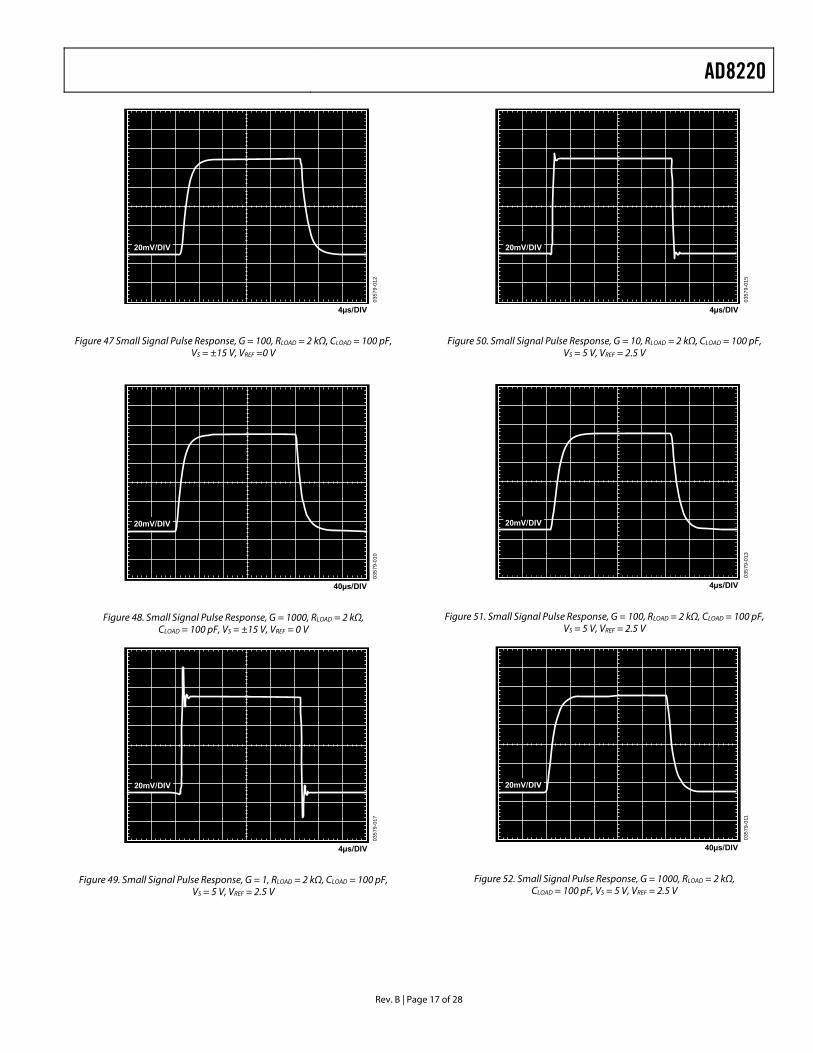
Figure 47 Small Signal Pulse Response, G = 100, RLOAD = 2 kΩ, CLOAD = 100 pF, VS = ±15 V, VREF =0 V
035
79-0
10
XXX
XX
X
20mV/DIV
40µs/DIV
Figure 48. Small Signal Pulse Response, G = 1000, RLOAD = 2 kΩ, CLOAD = 100 pF, VS = ±15 V, VREF = 0 V
035
79-0
17
XXX
XX
X
4µs/DIV
20mV/DIV
Figure 49. Small Signal Pulse Response, G = 1, RLOAD = 2 kΩ, CLOAD = 100 pF, VS = 5 V, VREF = 2.5 V
035
79-0
15
XXX
XX
X
4µs/DIV
20mV/DIV
Figure 50. Small Signal Pulse Response, G = 10, RLOAD = 2 kΩ, CLOAD = 100 pF, VS = 5 V, VREF = 2.5 V
035
79-0
13
XXX
XX
X
4µs/DIV
20mV/DIV
Figure 51. Small Signal Pulse Response, G = 100, RLOAD = 2 kΩ, CLOAD = 100 pF, VS = 5 V, VREF = 2.5 V
035
79-0
11
XXX
XX
X
40µs/DIV
20mV/DIV
Figure 52. Small Signal Pulse Response, G = 1000, RLOAD = 2 kΩ, CLOAD = 100 pF, VS = 5 V, VREF = 2.5 V
AD8220
Rev. B | Page 18 of 28
15
00 20
035
79-
043
OUTPUT VOLTAGE STEP SIZE (V)
SE
TT
LIN
G T
IME
(µ
s) 10
5
5 10 15
SETTLED TO 0.01%
SETTLED TO 0.001%
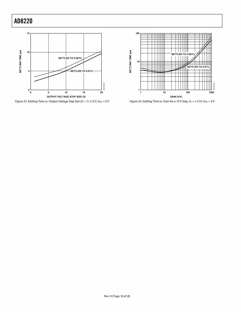
Figure 53. Settling Time vs. Output Voltage Step Size (G = 1) ±15 V, VREF = 0 V
100
11 1000
035
79-
041
GAIN (V/V)
SE
TT
LIN
G T
IME
(µ
s)
10 100
10
SETTLED TO 0.01%
SETTLED TO 0.001%
Figure 54. Settling Time vs. Gain for a 10 V Step, VS = ±15 V, VREF = 0 V
AD8220
Rev. B | Page 19 of 28
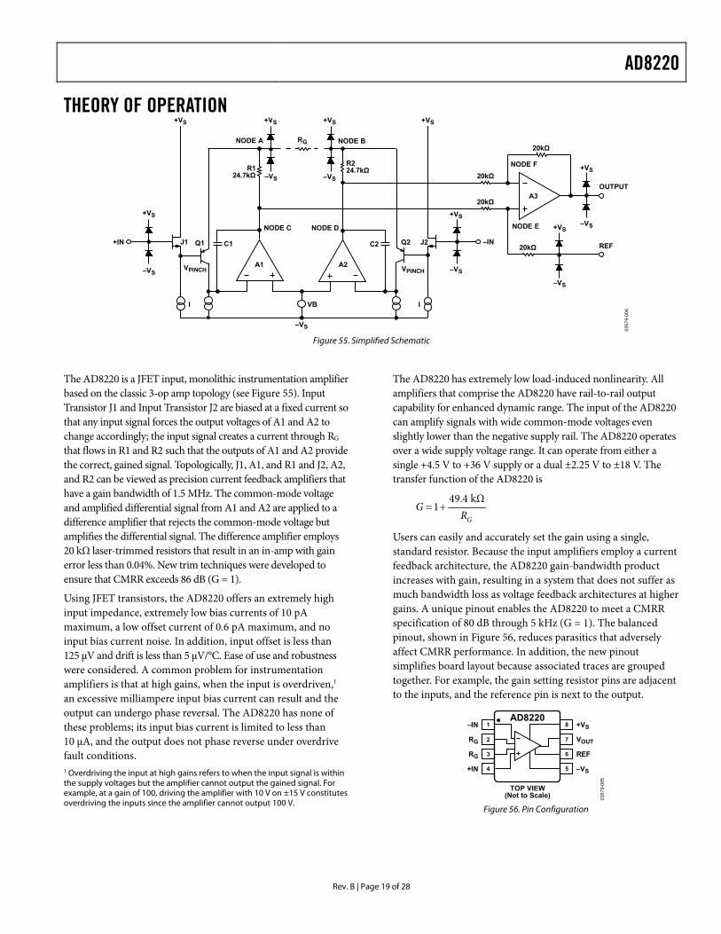
THEORY OF OPERATION
Q2Q1
NODE A NODE B
NODE C NODE D
VB
C1 C2
A1 A2
–VS
+VS
–VS
J1+IN
VPINCH
+VS
–VS
J2 –IN
VPINCH
+VS
–VS
RG
+VS +VS+VS
–VS
20kΩ
20kΩ
20kΩ
20kΩ
+VS
–VS
+VS
–VS
REF
OUTPUTA3
NODE E
NODE F
I I
R224.7kΩR1
24.7kΩ
0357
9-00
6
Figure 55. Simplified Schematic
The AD8220 is a JFET input, monolithic instrumentation amplifier based on the classic 3-op amp topology (see Figure 55). Input Transistor J1 and Input Transistor J2 are biased at a fixed current so that any input signal forces the output voltages of A1 and A2 to change accordingly; the input signal creates a current through RG that flows in R1 and R2 such that the outputs of A1 and A2 provide the correct, gained signal. Topologically, J1, A1, and R1 and J2, A2, and R2 can be viewed as precision current feedback amplifiers that have a gain bandwidth of 1.5 MHz. The common-mode voltage and amplified differential signal from A1 and A2 are applied to a difference amplifier that rejects the common-mode voltage but amplifies the differential signal. The difference amplifier employs 20 kΩ laser-trimmed resistors that result in an in-amp with gain error less than 0.04%. New trim techniques were developed to ensure that CMRR exceeds 86 dB (G = 1).
Using JFET transistors, the AD8220 offers an extremely high input impedance, extremely low bias currents of 10 pA maximum, a low offset current of 0.6 pA maximum, and no input bias current noise. In addition, input offset is less than 125 μV and drift is less than 5 μV/°C. Ease of use and robustness were considered. A common problem for instrumentation amplifiers is that at high gains, when the input is overdriven,1 an excessive milliampere input bias current can result and the output can undergo phase reversal. The AD8220 has none of these problems; its input bias current is limited to less than 10 μA, and the output does not phase reverse under overdrive fault conditions. 1 Overdriving the input at high gains refers to when the input signal is within the supply voltages but the amplifier cannot output the gained signal. For example, at a gain of 100, driving the amplifier with 10 V on ±15 V constitutes overdriving the inputs since the amplifier cannot output 100 V.
The AD8220 has extremely low load-induced nonlinearity. All amplifiers that comprise the AD8220 have rail-to-rail output capability for enhanced dynamic range. The input of the AD8220 can amplify signals with wide common-mode voltages even slightly lower than the negative supply rail. The AD8220 operates over a wide supply voltage range. It can operate from either a single +4.5 V to +36 V supply or a dual ±2.25 V to ±18 V. The transfer function of the AD8220 is
GRG
kΩ49.41
Users can easily and accurately set the gain using a single, standard resistor. Because the input amplifiers employ a current feedback architecture, the AD8220 gain-bandwidth product increases with gain, resulting in a system that does not suffer as much bandwidth loss as voltage feedback architectures at higher gains. A unique pinout enables the AD8220 to meet a CMRR specification of 80 dB through 5 kHz (G = 1). The balanced pinout, shown in Figure 56, reduces parasitics that adversely affect CMRR performance. In addition, the new pinout simplifies board layout because associated traces are grouped together. For example, the gain setting resistor pins are adjacent to the inputs, and the reference pin is next to the output.
TOP VIEW(Not to Scale)
035
79-0
05
–IN 1
RG 2
RG 3
+IN 4
+VS8
VOUT7
REF6
–VS5
AD8220
Figure 56. Pin Configuration

AD8220
Rev. B | Page 20 of 28
GAIN SELECTION Placing a resistor across the RG terminals sets the AD8220 gain, which can be calculated by referring to Table 5 or by using the gain equation
1kΩ4.49
G
RG
Table 5. Gains Achieved Using 1% Resistors 1% Standard Table Value of RG (Ω) Calculated Gain 49.9 k 1.990 12.4 k 4.984 5.49 k 9.998 2.61 k 19.93 1.00 k 50.40 499 100.0 249 199.4 100 495.0 49.9 991.0
The AD8220 defaults to G = 1 when no gain resistor is used. Gain accuracy is determined by the absolute tolerance of RG. The TC of the external gain resistor increases the gain drift of the instrumentation amplifier. Gain error and gain drift are kept to a minimum when the gain resistor is not used.
LAYOUT Careful board layout maximizes system performance. In applications that need to take advantage of the low input bias current of the AD8220, avoid placing metal under the input path to minimize leakage current. To maintain high CMRR over frequency, lay out the input traces symmetrically and lay out the traces of the RG resistor symmetrically. Ensure that the traces maintain resistive and capacitive balance; this holds for additional PCB metal layers under the input and RG pins. Traces from the
gain setting resistor to the RG pins should be kept as short as possible to minimize parasitic inductance. An example layout is shown in Figure 57 and Figure 58. To ensure the most accurate output, the trace from the REF pin should either be connected to the AD8220 local ground (see Figure 59) or connected to a voltage that is referenced to the AD8220 local ground.
Common-Mode Rejection Ratio (CMRR)
The AD8220 has high CMRR over frequency giving it greater immunity to disturbances, such as line noise and its associated harmonics, in contrast to typical in-amps whose CMRR falls off around 200 Hz. These in-amps often need common-mode filters at the inputs to compensate for this shortcoming. The AD8220 is able to reject CMRR over a greater frequency range, reducing the need for input common-mode filtering.
A well-implemented layout helps to maintain the high CMRR over frequency of the AD8220. Input source impedance and capacitance should be closely matched. In addition, source resistance and capacitance should be placed as close to the inputs as possible.
Grounding
The output voltage of the AD8220 is developed with respect to the potential on the reference terminal. Care should be taken to tie REF to the appropriate local ground (see Figure 59).
In mixed-signal environments, low level analog signals need to be isolated from the noisy digital environment. Many ADCs have separate analog and digital ground pins. Although it is convenient to tie both grounds to a single ground plane, the current traveling through the ground wires and PC board can cause a large error. Therefore, separate analog and digital ground returns should be used to minimize the current flow from sensitive points to the system ground.
03
57
9-1
01
Figure 57. Example Layout—Top Layer of the AD8220 Evaluation Board
03
57
9-1
02
Figure 58. Example Layout—Bottom Layer of the AD8220 Evaluation Board

AD8220
Rev. B | Page 21 of 28
REFERENCE TERMINAL The reference terminal, REF, is at one end of a 20 kΩ resistor (see Figure 55). The output of the instrumentation amplifier is referenced to the voltage on the REF terminal; this is useful when the output signal needs to be offset to voltages other than common. For example, a voltage source can be tied to the REF pin to level-shift the output so that the AD8220 can interface with an ADC. The allowable reference voltage range is a function of the gain, common-mode input, and supply voltages. The REF pin should not exceed either +VS or −VS by more than 0.5 V.
For best performance, especially in cases where the output is not measured with respect to the REF terminal, source impedance to the REF terminal should be kept low, because parasitic resistance can adversely affect CMRR and gain accuracy.
POWER SUPPLY REGULATION AND BYPASSING The AD8220 has high PSRR. However, for optimal performance, a stable dc voltage should be used to power the instrumentation amplifier. Noise on the supply pins can adversely affect performance. As in all linear circuits, bypass capacitors must be used to decouple the amplifier.
A 0.1 μF capacitor should be placed close to each supply pin. A 10 μF tantalum capacitor can be used further away from the part (see Figure 59). In most cases, it can be shared by other precision integrated circuits.
AD8220
+VS
+IN
–IN
LOADREF
0.1µF 10µF
0.1µF 10µF
–VS
VOUT
03
57
9-0
01
Figure 59. Supply Decoupling, REF and Output Referred to Ground
INPUT BIAS CURRENT RETURN PATH The AD8220 input bias current is extremely small at less than 10 pA. Nonetheless, the input bias current must have a return path to common. When the source, such as a transformer, cannot provide a return current path, one should be created (see Figure 60).
+VS
REF
TRANSFORMER
–VS
AD8220
AC-COUPLED
+VS
REF
C
R
R
C
–VS
AD82201fHIGH-PASS =
2πRC
03
57
9-0
02
Figure 60. Creating an IBIAS Path
INPUT PROTECTION All terminals of the AD8220 are protected against ESD. (ESD protection is guaranteed to 4 kV, human body model.) In addition, the input structure allows for dc overload conditions a diode drop above the positive supply and a diode drop below the negative supply. Voltages beyond a diode drop of the supplies cause the ESD diodes to conduct and enable current to flow through the diode. Therefore, an external resistor should be used in series with each of the inputs to limit current for voltages above +Vs. In either scenario, the AD8220 safely handles a continuous 6 mA current at room temperature.
For applications where the AD8220 encounters extreme overload voltages, as in cardiac defibrillators, external series resistors and low leakage diode clamps, such as BAV199Ls, FJH1100s, or SP720s, should be used.

AD8220
Rev. B | Page 22 of 28
RF INTERFERENCE RF rectification is often a problem in applications where there are large RF signals. The problem appears as a small dc offset voltage. The AD8220 by its nature has a 5 pF gate capacitance, CG, at its inputs. Matched series resistors form a natural low-pass filter that reduces rectification at high frequency (see Figure 61). The relationship between external, matched series resistors and the internal gate capacitance is expressed as follows:
GDIFF RC
FilterFreqπ2
1
GCM RC
FilterFreqπ2
1
AD8220VOUT
CG
CG–VS
REF
–VS
R
R
+IN
–IN
+15V
–15V
0.1µF 10µF
0.1µF 10µF
035
79-0
30
Figure 61. RFI Filtering Without External Capacitors
To eliminate high frequency common-mode signals while using smaller source resistors, a low-pass RC network can be placed at the input of the instrumentation amplifier (see Figure 62). The filter limits the input signal bandwidth according to the following relationship:
)2(π21
GCDDIFF CCCR
FilterFreq
)(π21
GCCM CCR
FilterFreq
Mismatched CC capacitors result in mismatched low-pass filters. The imbalance causes the AD8220 to treat what would have been a common-mode signal as a differential signal. To reduce the effect of mismatched external CC capacitors, select a value of CD greater than 10 times CC. This sets the differential filter frequency lower than the common-mode frequency.
R
R
AD8220
+15V
+IN
–IN
0.1µF 10µF
10µF0.1µF
REF
VOUT
–15V
CD
CC
CC
10nF
1nF
1nF
4.02kΩ
4.02kΩ
0357
9-00
3
Figure 62. RFI Suppression
COMMON-MODE INPUT VOLTAGE RANGE The common-mode input voltage range is a function of the input range and the outputs of Internal Amplifier A1, Internal Amplifier A2, and Internal Amplifier A3, the reference voltage, and the gain. Figure 27 to Figure 30 show common-mode voltage ranges for various supply voltages and gains.
DRIVING AN ADC An instrumentation amplifier is often used in front of an ADC to provide CMRR and additional conditioning, such as a voltage level shift and gain (see Figure 63). In this example, a 2.7 nF capacitor and a 1 kΩ resistor create an antialiasing filter for the AD7685. The 2.7 nF capacitor also serves to store and deliver the necessary charge to the switched capacitor input of the ADC. The 1 kΩ series resistor reduces the burden of the 2.7 nF load from the amplifier. However, large source impedance in front of the ADC can degrade THD.
The example shown in Figure 63 is for sub-60 kHz applications. For higher bandwidth applications where THD is important, the series resistor needs to be small. At worst, a small series resistor can load the AD8220, potentially causing the output to overshoot or ring. In such cases, a buffer amplifier, such as the AD8615, should be used after the AD8220 to drive the ADC.
AD8220AD7685
4.7µF
ADR435
+5V
2.7nFREF
1kΩ1.07kΩ
+2.5V
+IN
–IN
±50mV
+5V
0.1µF10µF03
579
-03
3
Figure 63. Driving an ADC in a Low Frequency Application

AD8220
Rev. B | Page 23 of 28
APPLICATIONS INFORMATION AC-COUPLED INSTRUMENTATION AMPLIFIER Measuring small signals that are in the noise or offset of the amplifier can be a challenge. Figure 64 shows a circuit that can improve the resolution of small ac signals. The large gain reduces the referred input noise of the amplifier to 14 nV/√Hz. Therefore, smaller signals can be measured because the noise floor is lower. DC offsets that would have been gained by 100 are eliminated from the AD8220 output by the integrator feedback network.
At low frequencies, the OP1177 forces the AD8220 output to 0 V. Once a signal exceeds fHIGH-PASS, the AD8220 outputs the amplified input signal.
AD8220
OP1177
R15.8kΩ
+VS
+IN
–IN
0.1µF
0.1µF
0.1µF
0.1µF10µF10µF
REF
C
1µF
–VS
–VS+VS
+VS
–VS
R499Ω
12πRC
fHIGH-PASS =
VREF
035
79-0
04
Figure 64. AC-Coupled Circuit
DIFFERENTIAL OUTPUT In certain applications, it is necessary to create a differential signal. New high resolution ADCs often require a differential input. In other cases, transmission over a long distance can require differential processing for better immunity to interference.
Figure 65 shows how to configure the AD8220 to output a differential signal. An OP1177 op amp is used to create a differential voltage. Errors from the op amp are common to both outputs and are thus common mode. Likewise, errors from using mismatched resistors cause a common-mode dc offset error. Such errors are rejected in differential signal processing by differential input ADCs or instrumentation amplifiers.
When using this circuit to drive a differential ADC, VREF can be set using a resistor divider from the reference of the ADC to make the output ratiometric with the ADC as shown in Figure 66.

AD8220
Rev. B | Page 24 of 28
±5V
0.1µF
+5V
–5V
4.99kΩ
4.99kΩ
AD8220
OP1177
+15V
+IN
–IN
0.1µF
0.1µF10µF
REF
+5V+15V–15V
VREF2.5V
VOUTA = +VIN + VREF
2
VOUTB = –VIN + VREF
2
0.1µF
–15V
+2.5V+5.0V
+0V
TIME
AMPLITUDE
+2.5V+5.0V
+0V
TIME
AMPLITUDE
TIME
AMPLITUDE
0357
9-0
08
Figure 65. Differential Output with Level Shift
±5V
0.1µF
4.99kΩ
4.99kΩ
4.99kΩ
4.99kΩ
AD8220
OP1177
+15V
+IN
–IN
0.1µF
0.1µF
10µF
REF
+5V+15V–15V
VREF2.5V
VOUTA = +VIN + VREF
2
0.1µF
–15V
TIME
TO 0V TO +5V ADC
TO 0V TO +5V ADC
+AIN
–AIN
REF
+5V FROM REFERENCE
+5V FROM REFERENCE
10nF
VOUTB = –VIN + VREF
2
035
79-0
31
Figure 66. Configuring the AD8220 to Output A Ratiometric, Differential Signal

AD8220
Rev. B | Page 25 of 28
ELECTROCARDIOGRAM SIGNAL CONDITIONING The AD8220 makes an excellent input amplifier for next generation ECGs. Its small size, high CMRR over frequency, rail-to-rail output, and JFET inputs are well suited for this application. Potentials measured on the skin range from 0.2 mV to 2 mV. The AD8220 solves many of the typical challenges of measuring these body surface potentials. The high CMRR of the AD8220 helps reject common-mode signals that come in the form of line noise or high frequency EMI from equipment in the operating room. Its rail-to-rail output offers a wide dynamic range allowing for higher gains than would be possible using other instrumentation amplifiers. JFET inputs offer a large input capacitance of 5 pF. A natural RC filter is formed reducing high frequency noise when series input resistors are used in front of the AD8220 (see the RF Interference section).
In addition, the AD8220 JFET inputs have ultralow input bias current and no current noise, making it useful for ECG applications where there are often large impedances. The MSOP and the optimal pinout of the AD8220 allow smaller footprints and more efficient layout, paving the way for next-generation portable ECGs.
Figure 67 shows an example ECG schematic. Following the AD8220 is a 0.033 Hz high-pass filter, formed by the 4.7 μF capacitor and the 1 MΩ resistor, which removes the dc offset that develops between the electrodes. An additional gain of 50, provided by the AD8618, makes use of the 0 V to 5 V input range of the ADC. An active, fifth-order, low-pass Bessel filter removes signals greater than approximately 160 Hz. An OP2177 buffers, inverts, and gains the common-mode voltage taken at the midpoint of the AD8220 gain setting resistors. This right-leg drive circuit helps cancel common-mode signals by inverting the common-mode signal and driving it back into the body. A 499 kΩ series resistor at the output of the OP2177 limits the current driven into the body.
ADC
AD7685AD8618
+5V
2.7nF
500Ω
AD8618
14.5kΩ19.3kΩ
2.5V
22nF
4.7µFREF+5V
REFERENCEADR435
68nF
+5V
AD8618
+5V
1.15kΩ
4.99kΩ
2.5V2.5V2.5V
33nF
19.3kΩ 14.5kΩ
33nF
LOW-PASS FIFTH ORDER FILTER AT 157Hz
AD8618
+5V
–5V
–5V
+5V
47nF
14kΩ14kΩ57.6kΩ1.18kΩ
G = +50
4.7µF
2.5V
1MΩ
12.7kΩ
499kΩ
220pF
HIGH-PASS FILTER 0.033Hz
INSTRUMENTATIONAMPLIFIER
G = +14
AD8220+5V
4.12kΩ24.9kΩ
24.9kΩ
–5V
+5V
OP AMPS
OP2177
OP2177
866kΩ
68pF
A B
C
03
579
-03
2
15kΩ
–5V
+5V–5V
+5V
2.2pF
2.2pF
10pF
10kΩ
10kΩ
Figure 67. Example ECG Schematic

AD8220
Rev. B | Page 26 of 28
OUTLINE DIMENSIONS
COMPLIANT TO JEDEC STANDARDS MO-187-AA 1007
09-B
6°0°
0.800.550.40
4
8
1
5
0.65 BSC
0.400.25
1.10 MAX
3.203.002.80
COPLANARITY0.10
0.230.09
3.203.002.80
5.154.904.65
PIN 1IDENTIFIER
15° MAX0.950.850.75
0.150.05
Figure 68. 8-Lead Mini Small Outline Package [MSOP]
(RM-8) Dimensions shown in millimeters
ORDERING GUIDE Model1, 2 Temperature Range3 Package Description Package Option Branding AD8220ARMZ −40°C to +85°C 8-Lead MSOP RM-8 H01 AD8220ARMZ-RL −40°C to +85°C 8-Lead MSOP, 13" Tape and Reel RM-8 H01 AD8220ARMZ-R7 −40°C to +85°C 8-Lead MSOP, 7" Tape and Reel RM-8 H01 AD8220BRMZ −40°C to +85°C 8-Lead MSOP RM-8 H0P AD8220BRMZ-RL −40°C to +85°C 8-Lead MSOP, 13" Tape and Reel RM-8 H0P AD8220BRMZ-R7 −40°C to +85°C 8-Lead MSOP, 7" Tape and Reel RM-8 H0P AD8220WARMZ −40°C to +125°C 8-Lead MSOP RM-8 Y2D AD8220WARMZ-RL −40°C to +125°C 8-Lead MSOP, 13" Tape and Reel RM-8 Y2D AD8220WARMZ-R7 −40°C to +125°C 8-Lead MSOP, 7" Tape and Reel RM-8 Y2D 1 Z = RoHS Compliant Part. 2 W = Qualified for Automotive Applications. 3 See the Typical Performance Characteristics section for expected operation from 85°C to 125°C.
AUTOMOTIVE PRODUCTS The AD8220W models are available with controlled manufacturing to support the quality and reliability requirements of automotive applications. Note that these automotive models may have specifications that differ from the commercial models; therefore, designers should review the Specifications section of this data sheet carefully. Only the automotive grade products shown are available for use in automotive applications. Contact your local Analog Devices account representative for specific product ordering information and to obtain the specific Automotive Reliability reports for these models.

AD8220
Rev. B | Page 27 of 28
NOTES

AD8220
Rev. B | Page 28 of 28
NOTES
©2006–2010 Analog Devices, Inc. All rights reserved. Trademarks and registered trademarks are the property of their respective owners. D03579-0-5/10(B)