Embed Size (px)
Citation preview
A bstrac t
A transition-edge-sensor-based instrument for the measurement of individual He2* excimers in a
superfluid 4He bath at 100 mK
Faustin Wirkus Carter
2015
This dissertation is an account of the first calorimetric detection of individual HeJ excimers
within a bath of superfluid 4He. When superfluid helium is subject to ionizing radiation,
diatomic He molecules are created in both the singlet and triplet states. The singlet He
molecules decay within nanoseconds, but due to a forbidden spin-flip the triplet molecules
have a relatively long lifetime of 13 seconds in superfluid He. When He^ molecules decay,
they emit a ~15 eV photon. Nearly all matter is opaque to these vacuum-UV photons,
although they do propagate through liquid helium. The triplet state excimers propagate
ballistically through the superfluid until they quench upon a surface; this process deposits
a large amount of energy into the surface. The prospect of detecting both excimer states is
the motivation for building a detector immersed directly in the superfluid bath.
The detector used in this work is a single superconducting titanium transition edge
sensor (TES). The TES is mounted inside a hermetically sealed chamber at the baseplate
of a dilution refrigerator. The chamber contains superfluid helium at 100 mK. Excimers
are created during the relaxation of high-energy electrons, which are introduced into the
superfluid bath either in situ via a sharp tungsten tip held above the field-emission voltage,
or by using an external gamma-ray source to ionize He atoms. These excimers either
propagate through the LHe bath and quench on a surface, or decay and emit vacuum-
ultraviolet photons that can be collected by the detector.
This dissertation discusses the design, construction, and calibration of the TES-based
excimer detecting instrument. It also presents the first spectra resulting from the direct
detection of individual singlet and triplet helium excimers.

A transition-edge-sensor-based instrum ent for the
m easurem ent o f individual He2* excim ers in a
superfluid 4He bath at 100 mK
A Dissertation Presented to the Faculty of the G raduate School
ofYale University
in Candidacy for the Degree of Doctor of Philosophy
byFaustin W irkus Carter
D issertation Director: Daniel E. Prober
December 2015

ProQuest Number: 10012481
All rights reserved
INFORMATION TO ALL USERS The quality of this reproduction is dependent upon the quality of the copy submitted.
In the unlikely event that the author did not send a complete manuscript and there are missing pages, these will be noted. Also, if material had to be removed,
a note will indicate the deletion.
ProQuest 10012481
ProQuestQ ue
Published by ProQuest LLC(2016). Copyright of the Dissertation is held by the Author.
All rights reserved.This work is protected against unauthorized copying under Title 17, United States Code.
Microform Edition © ProQuest LLC.
ProQuest LLC 789 East Eisenhower Parkway
P.O. Box 1346 Ann Arbor, Ml 48106-1346

Copyright © 2015 by Faustin Wirkus Carter
All rights reserved.
Acknowledgements
It takes a lot of people to produce a PhD. There is not room to mention every person who
has contributed to the success of my journey (this dissertation would be twice as long if I
tried), but here I will give thanks at least to the regulars: the people who keep showing
up, and helping, and giving, and talking, and pushing, and without whom I would have
probably gone completely bonkers!
My immediate family: Lauren Gregory has been by my side from almost the very
beginning of my young career in physics and has been a constant source of love, support,
perspective, humor, and encouragement. I don’t know if she knew quite what she was
getting into when she signed on as “life partner,” but I’m sure glad to have her along for
the ride! Dr. Russell Carter, my brother, against whom I have recently (and proudly) lost
the competition to be the first PhD in the family, has been my best friend for my whole
life and a sounding board for most of my life choices. Lydia Wirkus, my mother, (who
now has two physicist sons to deal with), taught me to ask lots of questions and think
for myself, encouraged me to focus on productivity rather than perfection, and instructed
me in the fine art of asking for forgiveness, not permission. Roger Carter, my (very) late
father, helped start me on this path by encouraging and nurturing a love for figuring out
how things (everything!) works when I was still young enough for it to stick. I can not
thank them enough.
My PhD adviser, Prof. Dan Prober, has been a cornerstone of my Yale experience. He
has encouraged me to explore and find my own answers, but has never accepted anything
less than my best. I have discovered tha t on a long enough time scale, Dan Prober is always
right; even if his advice doesn’t make sense right away, it is best not to forget it as it will
eventually prove to be crucial. I am proud to be part of the Prober Lab extended family!
I owe a great debt of gratitude to Prof. Michel Devoret. His gracious loan of a dilution
refrigerator (for three years!), endless amounts of equipment, and the time of his postdocs
is what made this project possible. W ithout his generosity this whole project would never
have made it past the “neat idea” stage, and for tha t I am thankful indeed.
The department (both physics and applied physics) staff: Giselle DeVito, Maria Rao,
Theresa Evangeliste, Sandy Tranquilli, and Devon Cimini are the reason the department
doesn’t fall apart every day and I am grateful to all of them for the tremendous amounts
of help they have given me throughout the years.
My dissertation committee: Prof. Dan McKinsey came up with the idea for this whole
project back in the beginning and was instrumental in supporting it, keeping things on track,
and moving everything forward. Dr. Andrew Szymkowiak has been an excellent source of
advice for everything from data filtering to choosing a career path. I am very thankful to
Prof. Liang Jiang, who donated his time and his perspective to this project. Prof. Rob
Schoelkopf served on my prospectus committee and, in addition to coming up with clever
names for the experiment (like Improvised Helium Device, or IHD), gave some great advice
on ground-loop mitigation and loaned me the computer I wrote this dissertation on. Prof.
Wei Guo’s postdoctoral work served as one of the foundations for this experiment and he
was always more than happy to explain how things work (at a deep level) and help us figure
out why things were sometimes “working” differently than they ought.
My direct collaborators: Scott Hertel, postdoc extroardinaire, was instrumental in mak
ing all of this come together, and none of it would have happened without him. He has been
a part of every success (but not every failure) and through it all has taught me a great deal.
I have been fortunate to have him as a colleague and a friend. Jeremy Cushman did most
of the CAD work and spent a lot of time down at the machine shop getting the experiment
built in the first year. Catherine Matulis helped us frantically rebuild our helium injection
lines under a looming deadline, and put a lot of work into the high-voltage electronics. I
am also grateful to E than Bernard, a McKinsey Lab postdoc, for loaning us equipment and
expertise over and over again.
The fabrication gurus: Dr. Luigi Frunzio and Dr. Mike Rooks taught me nearly ev
erything I know about the art of fabricating very small things. Luigi has been a constant
(and audible!) source of good cheer, good advice, good 2” wafers, and the occasionally
necessary reality check. Mike has always kept his office door open (a policy I have taken
huge advantage of) and has been both a mentor and a friend. Also, I must thank “the
guys upstairs”: Mike Power, Chris Tillinghast, and Jim Agresta have always entertained
my frantic requests for a spare part or a last-minute clean-room job.
My lab: Chris McKitterick joined Prober Lab with me as a fellow first year and was
a constant source of friendship, encouragement, advice (some better than others), and (of
course) exasperation! I can’t imagine having gone through Yale without him; it would have
been a measurably poorer experience. Prof. Daniel Santavicca was a postdoc when I first
arrived and taught me almost everything I know about measuring anything at all. Even
after embarking upon a faculty job of his own, he was always a phone call away and never
too busy to help. When I am confused I repeat the m antra “W hat would Dan Santavicca
do?” and my path becomes more clear.
My colleagues: Prof. Michael Hatridge, with whom I share a deep love for all the shared
virtues of Alaska and Texas, schooled me in the fine art of the dilution refrigerator, and
was a model of the kind of postdoc I hope to become. K atrina Sliwa and Anirudh Narla
spent hours and hours of their valuable time helping me diagnose an endless parade of
technical (and occasional scotch-related) issues over the years. Chris Axline allowed me to
maximize my laziness by automating nearly every piece of hardware I relied on and doubled
as an excellent flying partner. Zaki Leghtas and Stephen Touzard were excellent cryostat
“roommates” and I owe much success to their patience and temperance. Additionally, nearly
everyone on the 4th floor of Becton Hall made a concrete difference at one point or another
and I am happy to count them as friends as well as colleagues; my inability to name each
person directly does not weaken their contributions.
My friends: Since my very first day at Yale, Brian Vlastakis and Jamie Benoit have
been at the top of my speed dial list. First as neighbors in HGS and later as collaborators
a t GPSCY, international travel companions, sharers of Christmas cheer, and all-around
excellent BBQ companions, these two remarkable fellows have been a fundamental constant
in my Yale life. I must also pay my regards to some other fine folks who have made my time
at Yale brighter. Naming friends is always a risky proposition, but the risk of forgetting a
few pales compared to the gratitude I feel and so I make a partial list here: Joe Belter, Eric
and Luanne Bohman, Alex Cerjan, Raphael Chevrier, Kyle Cromer, Jane Cummings, Prank
and Taby (Ali) Francese, Jenny Fribourgh, Kseniya Gavrilov, Brad Hayes, Eric Holland,
Larry Lee, Colton Lynner, Pete Manza, Drew Mazurek, Ramiro Nandez, Erica Nelson, Ariel
Niell, Josh Nilaya, Helen Rankin, Jenny Schmitzer, Adam Simpson, the GPSCY Staff and
Softball team, the G rad/P rof pickup hockey team, et. al. I ’m not sure I ’m supposed to
admit to having had a rich and vibrant social life while also getting my PhD, but I did, and
it is thanks to these people (and many others).
Finally, my six years at Yale and my research were made possible by financial support
from the Yale Physics department, the Yale Applied Physics department, the National
Science Foundation (NSF), the National Aeronautics and Space Administration (NASA),
and IBM. I thank all of them for paying my bills and rent, and buying all the pieces of my
science project, which you can read about in the following pages!
Contents
Acknowledgements iii
List o f figures xi
List o f tables xiii
Introduction 1
1 Helium excim ers 3
1.1 Vortices in superfluid helium ................................................................................. 4
1.2 Direct dark m atter detection ................................................................................... 5
1.3 Candidate technologies for detecting He^ e x c im e rs ........................................... 6
1.3.1 Photomultipliers and avalanche photodiodes........................................... 7
1.3.2 C C D s ................................................................................................................. 7
1.3.3 Optical pumping measurements of He^ excimers ................................. 7
1.3.4 Superconducting tunnel junc tio n s .............................................................. 8
2 Transition edge sensors 10
2.1 Electro-thermal feedback............................................................................................ 11
2.1.1 TES thermal c i r c u i t ...................................................................................... 12
2.1.2 TES electrical c ircu it...................................................................................... 13
2.2 Numerical solutions to TES e q u a t io n s ................................................................. 14
2.3 Small signal response.................................................................................................. 18
2.3.1 Pulse m o d e l....................................................................................................... 19
2.3.2 TES noise and energy re s o lu t io n .............................................................. 21
3 Experiment design 26
3.1 Helium p lu m b in g ......................................................................................................... 28
3.1.1 Plumbing inside the c r y o s t a t ..................................................................... 29
3.1.2 Plumbing outside the cryosta t..................................................................... 32
3.2 SQUID am plifiers......................................................................................................... 33
3.3 Low voltage w ir in g ...................................................................................................... 35
3.4 High voltage electronics and w irin g ......................................................................... 35
3.5 Fiber o p t ic s ................................................................................................................... 37
4 TES design and fabrication 39
4.1 TES m ateria ls ................................................................................................................ 39
4.2 F a b r ic a tio n ................................................................................................................... 42
4.2.1 Alignment m a rk s ........................................................................................... 43
4.2.2 T i/A l b i la y e r .................................................................................................. 43
4.2.3 A1 etch ............................................................................................................ 43
4.2.4 Shield fabrication ........................................................................................... 43
4.3 Description of TESs used in e x p e r im e n t.............................................................. 44
4.3.1 TES A: bare TES ......................................................................................... 44
4.3.2 TES B: shielded TES number 1 .................................................................. 44
4.3.3 TES C: TES with reflective substrate ..................................................... 46
4.3.4 TES D, E, and F: shielded TES number 2 ............................................... 46
4.3.5 Devices G, H, and I: the two-TES detector ........................................... 47
5 D etector characterization 49
5.1 TES current ( / t e s ) vs- bias current (7 b ) .............................................................. 51
5.1.1 Parasitic (Rp) and normal (7?n) resistance............................................... 51
5.1.2 Critical current (Jc) and critical tem perature (Tc) .................................. 53
5.2 TES Joule power (T*tes) vs- bias current ( 7 b ) ..................................................... 53
5.2.1 Thermal conductance (Ge-ph) and thermal exponent ( n ) .................... 54
viii
5.3 Temperature ( I tes) vs. bias current (/b) .......................................................... 57
5.3.1 TES sensitivity to temperature (a /) and current (/?/) 57
5.3.2 TES heat capacity (Ce) ............................................................................... 58
5.4 TES n o is e ..................................................................................................................... 59
5.5 Photon d e te c tio n ....................................................................................................... 61
6 TES calibrations 64
6.1 Photon detection with TESs A, B, and C .......................................................... 65
6.1.1 TES A: understanding substrate ab so rp tio n .................................. 65
6.1.2 TES B: blocking substrate absorption with an in situ aperture . . . 69
6.1.3 TES C: blocking substrate absorption with a substrate mirror . . . . 71
6.2 Photon detection with TESs D, E, and F .......................................................... 72
6.2.1 TES D: searching for the source of an extra unwanted signal . . . . 72
6.2.2 TES F: considering photon absorptions near the TES edge .............. 75
6.3 Calibration algorithm .............................................................................................. 79
6.3.1 Preprocessing algorithm applied to all traces ........................................ 80
6.3.2 Creating a model single photon p u lse ........................................................ 81
6.3.3 Using the pulse model and the noise traces to build a better filter . . 82
6.3.4 Processing algorithm for experimental d a t a ........................................... 83
7 Helium excim er detections 85
7.1 Excimers created via gamma-ray e x c i ta t io n ....................................................... 86
7.1.1 Spectra from 22Na irrad ia tio n ..................................................................... 87
7.1.2 Response to varying 3He concentration..................................................... 90
7.2 Excimers created via high electric f ie ld ................................................................. 91
7.2.1 Response to varying tip v o ltag e .................................................................. 92
7.3 D iscussion..................................................................................................................... 93
7.3.1 UV photon coupling to T E S s ..................................................................... 94
7.3.2 Triplet excimer coupling to T E S ............................................................... 96
ix
8 N ext steps 101
8.1 Engineering improvements for version 2 ............................................................. 101
8.1.1 E le c tro n ic s ..................................................................................................... 101
8.1.2 LHe c h a m b e r .................................................................................................. 103
8.1.3 T E S .................................................................................................................. 104
8.2 Future science goals ................................................................................................. 105
8.3 Concluding remarks ................................................................................................. 106
Appendices
A TES absorber diffusion m ath 108
A .l Diffusion e q u a t io n .................................................................................................... 109
A.2 Solving for the number of quasiparticles in the TES detector ...................... 112
A.3 Adding loss in the superconducting absorber....................................................... 113
A.4 The 2-D c a s e .............................................................................................................. 114
A.5 Adding the effects of finite trapping time to the 1-D ca se ................................ 116
B Plum bing circuits 118
C Computer code 124
C .l TES differential e q u a tio n s ....................................................................................... 124
C.2 Diffusion equation .................................................................................................... 130
D Fabrication recipes 133
D .l Wafer c le a n in g ........................................................................................................... 133
D.2 Single layer r e s is t ........................................................................................................ 133
D.3 Bilayer resist .............................................................................................................. 134
D.4 Copper evaporation.................................................................................................... 134
D.5 T i/A l bilayer e v a p o ra tio n ....................................................................................... 135
D.6 L ift-off........................................................................................................................... 135
D.7 A1 e tc h in g .................................................................................................................... 135
D.8 Cu etching..................................................................................................................... 135
x
D.9 Electron beam lithography: writing and developing......................................... 136
D.9.1 Beam current and dose .............................................................................. 136
D.9.2 Developing E-beam r e s i s t ........................................................................... 136
E Sources o f noise and interference 137
E .l Computers (and other electronics) ....................................................................... 138
E.2 Overhead l ig h ts ........................................................................................................... 139
E.3 V ib ra tions .................................................................................................................... 140
xi

List of figures
2.1 TES thermal c i r c u i t ................................................................................................... 13
2.2 TES electrical c irc u it................................................................................................... 14
2.3 Simulation of TES current vs. bias current ........................................................ 16
2.4 Effects of parameter variations on TES bias cu rve............................................... 17
2.5 Quantities derived from TES bias c u r v e ............................................................... 18
2.6 Simulated response of TES to a single p h o to n ..................................................... 21
2.7 Effect of varying parameters on TES pulse rise and fall t i m e s ......................... 22
2.8 TES noise m o d e l ......................................................................................................... 24
3.1 Experimental c h a m b e r ................................................................................................ 27
3.2 Gas handling s y s te m ................................................................................................... 29
3.3 Internal plumbing d iagram ......................................................................................... 30
3.4 Beer kegs as vacuum v esse ls ...................................................................................... 33
3.5 Wiring diagram, and view of inside of experimental chamber ........................ 34
3.6 High voltage tip a ssem b ly ......................................................................................... 36
3.7 High voltage wiring h e a ts in k s ................................................................................... 36
4.1 Optical microscope images of TESs A, B, and C ............................................... 45
4.2 Optical and SEM microscope images of TES D .................................................. 47
4.3 Optical microscope images of TESs G, H, and I .................................................. 48
5.1 Model fits to TES bias curve and TES p u lse ......................................................... 50
5.2 TES bias curve and calculated resistance c u r v e .................................................. 52
5.3 Measuring TES Joule p o w er...................................................................................... 55
5.4 Superconducting transition for DC and ETF TES o p e ra tio n ........................... 57
5.5 Plots of a iv and tem perature for TES D ............................................................... 59
5.6 Measured TES A n o ise ................................................................................................ 60
5.7 TES B photon response at different a t te n u a t io n s ............................................... 63
6.1 Response of TES A to blue and IR l i g h t ............................................................... 66
6.2 TES B bias curve and photon response.................................................................. 70
6.3 TES C photon re s p o n s e ............................................................................................ 71
6.4 TES D photon re s p o n s e ............................................................................................ 74
6.5 TES F photon response; calculations of quasiparticle diffusion in the leads . 76
6.6 TES F photon response after p ro cessin g ............................................................... 78
7.1 TES response to gamma-rays with and without superfluid h e liu m ................. 86
7.2 Coincidence measurement experimental s e t u p ..................................................... 88
7.3 Excimer signal with and without PM T coincidence........................................... 89
7.4 Comparison of excimer signal with pure 4He and with some 3He added . . . 90
7.5 TES response to excimers created via electron b o m b a rd m e n t........................ 92
7.6 Excimer signal as a function of absolute tip voltage for TESs D, E, and F . 94
7.7 Scintillation spectrum from electron-bombarded helium .................................. 95
7.8 Process by which triplet excimers couple to a T E S ........................................... 98
A .l Two-pixel TES signal for various absorber lengths ........................................... 117
D .l Lift-off p r o c e s s ............................................................................................................. 134
E .l Computer power cord wrapped around ferrite donut co re .................................. 139
xiii

List of tables
2.1 Definitions of quantities used in the small-signal m o d e l..................................... 19
4.1 A list of TESs measured in this work....................................................................... 44
5.1 Parameter values corresponding to numerical f i t s ............................................... 51
C .l Parameter values corresponding to numerical m o d e ls ........................................ 125
Introduction
THIS dissertation is an account of the construction of an instrument tha t is capable
of calorimetric detection of individual He^ excimers within in a bath of superfluid
4He. When superfluid helium is subject to ionizing radiation, diatomic He molecules are
created in both the singlet and triplet states. The singlet He^ molecules decay within
nanoseconds, but due to a forbidden spin-flip the triplet molecules have a relatively long
lifetime of 13 seconds in superfluid He. For this reason, triplet He^ molecules are useful
as tracers for studying fluid flow and turbulence in liquid helium (LHe) (Guo et al., 2014).
The singlet molecules also may be useful in the search for dark m atter as some He molecules
should be created by recoiling 4He atoms scattered by weakly interacting massive particles
(WIMPs) passing through a reservoir of LHe (Guo and McKinsey, 2013). When a He?;
molecule decays, it emits a ~15 eV photon. Nearly all m atter is opaque to these vacuum-
UY photons, although they do propagate through liquid helium, which is the motivation for
building a detector immersed directly in the superfluid bath. The detection of He?j excimers
in general is discussed in more detail in chapter 1.
The detector used in this work consists of a single superconducting titanium transition
edge sensor (TES). TES physics and operating principles are the subject of chapter 2. The
TES can operate at any temperature from the cryostat base temperature of ~20 mK to
just below its transition temperature (Tc = 430 mK) and so this, in principle, allows one
to study He?; excimers over a wide range of temperatures. The design and fabrication of
the TESs used in this project are the subject of chapter 4, and the initial characterization
of the TESs is detailed in chapter 5. The TESs are mounted inside a hermetically sealed
chamber attached to the bottom of a dilution refrigerator. The chamber is filled with
superfluid helium. The chamber and all the associated experimental hardware are described
in chapter 3. Inside the chamber is a sharp tungsten tip tha t may be operated at a high
voltage (up to a few kV) in order to ionize He atoms and create He^ excimers. These
excimers either propagate through the LHe bath and then quench on a surface, or decay
into vacuum-ultraviolet photons tha t are collected by the detector. This basic experiment
is not new. Zmeev et al. (2013a,b) have recently accomplished the detection of a cloud of
He?! excimers over a range of temperatures. Their detector relies on ionizing an excimer
and collecting the resulting free electron on either a copper plate or a fine wire mesh. This
process is very inefficient and requires averaging the data over several days to achieve a
reasonable signal-to-noise ratio. The TES-based detector described in this work is sensitive
to individual excimers, requires no averaging, and can also detect the energy spectrum of
the detected molecules (or photons). The first detections of individual helium excimers
are the subject of chapter 7, and the calibration process required to interpret the helium
excimer data is discussed in chapter 6.
One of the original aims of this project was to not only make a TES detector that
could see individual excimers, but to make a detector tha t was readily scalable in area to
be up to several millimeters long with some position resolution. Several prototype devices
designed with scalability and position resolution in mind were fabricated, but an unforseen
issue with the measurement electronics (see section 4.3.5) precluded any of them from being
successfully measured. Regardless, given the success of the detectors tha t were measured,
there is no reason why the unmeasured prototypes should not work as designed. The
operating principles of this scalable device, as well as a calculation of expected performance
(based on an extrapolation of the working TESs measured over the course of this project)
is available in appendix A.
Finally, several decisions were made during the initial planning stages of the experiment
that, with the benefit of hindsight, turned out to be suboptimal. The concluding chapter
discusses these lessons learned, and will hopefully be of use to anyone who wishes to try
something similar.
2
Helium excimersChapter
A h e l i u m excimer is a diatomic molecule of helium atoms, which exists in an excited
state (the word excimer is a portm anteau of “excited” and “dimer”) . Ordinarily, he
lium does not form a bound state as it is a noble gas, and all of its electron orbitals are
full. However, when a helium atom has one of its electrons excited to a higher energy level,
the potential energy as a function of inter-atomic spacing (usually a curve tha t increases
monotonically with decreasing separation distance) develops a shallow local minimum, al
lowing a metastable bound state of two atoms to form. This bound state, called He^ (the
denotes excitation) has an energy tha t is 13-20 eV above the He ground state, and so
releases a vacuum UV photon upon decay. The singlet state He2 (A1£ u) decays within a
few ns. The triplet state He2 («3£ u) decay process involves a spin flip tha t is forbidden by
selection rules and so its lifetime is ~13 s in superfluid helium (McKinsey et al., 1999).
The production of He?; in superfluid helium can be straightforward: any process that
either ionizes helium atoms (He+ + H e > H e^, He^ + He + e- ► He^ + He) or excites
helium atoms with sufficient energy (He* + 2 H e 1 He^ + He) can result in the creation of
excimers. This includes (but is not necessarily limited to) nuclear scattering from neutrons
and alpha particles, electronic scattering from gamma-rays, beta particles, and high-energy
electrons (Keto et al., 1972, 1974; Tokaryk et al., 1993), and ionization from femtosecond
laser pulses (Benderskii et al., 1999). A common way to create high-energy electrons in
situ is to bias a sharp tungsten tip at a voltage above the electron-emission threshold. In
this work, excimers were created in two ways: through the electron-emission of a tung
sten tip, and through gamma-ray scattering using a 22Na gamma-ray emitter, which emits
511 keV and 1.3 MeV gamma-rays. Both of these processes create excimers through elec
tronic scattering, which results in the production of excimers in a roughly 4:1 singlet;triplet
ratio (Sato et al., 1974), and also through the geminate recombination of electron ion pairs,
which results in a 1:1 singlet:triplet ratio (Adams, 2001).
The detection of individual He^ molecules in superfluid helium is the subject of this
dissertation. The following two sections contain brief examples of applications where one
might be interested in detecting He^, and the final section in this chapter gives an overview
of He?; detection methods tha t are currently available.
1.1 Vortices in superfluid helium
When liquid helium undergoes a phase transition to the superfluid state, the superfluid
component does not admit angular momentum; the curl of the velocity is zero. Instead,
angular momentum is confined to quantized vortices with normal fluid cores, which align
parallel to the axis of rotation. This is analogous to how a type-II superconductor expels
magnetic flux, confining it in quantized amounts through small normal regions. Each vortex
is associated with a quantum of angular momentum. For a volume of superfluid rotating
at a constant angular velocity, these vortices will form a regular lattice with the angular
momentum parallel to the axis of rotation. However, for turbulent systems, the vortices
will become chaotic and tangled, a condition known as quantum turbulence (see Aarts and
de Waele (1994) for a discussion of vortex tangles and some excellent visualizations). The
rotational energy of a vortex is oc ln(r/ro) where r is the separation between vortices and ro
is the radius of the vortex core (McClintock et al., 1984). Consequently, the energy of the
vortex is reduced by increasing the radius; this promotes the entrainment of small particles
in the vortex core. The “decoration” of vortices by small particles, which may then be
imaged by standard means, is one of the primary methods of studying superfluid vortices
and quantum turbulence (Zhang et al., 2004; Zhang and Van Sciver, 2005).
4
The particles used for tagging the vortices in this way would ideally be easily observed,
long-lived, and small in diameter so as not to perturb the vortex dynamics under study.
Micron-scale hydrogen ice particles have been used to visualize vortices, observe vortex
reconnection, study Kelvin waves, and to measure thermal counterflow (Bewley et al., 2006;
La M antia et al., 2012; Bewley et al., 2008; Paoletti et al., 2008; Sergeev and Barenghi, 2009).
Despite the success with hydrogen ice, Heg excimers produced in situ through electron
bombardment or laser ionization offer significant advantages. He^ is the third smallest
helium-only tracer particle (only 3He atoms and H eJ ions are smaller) and is efficiently and
permanently trapped by quantum vortices (trapping radius ~100 nm (Zmeev et al., 2013a)).
Unlike 3He atoms, He^ excimers do not constitute an impurity in a superfluid 4He bath in
the sense tha t they arise from, and decay to, 4He atoms. Although there are ongoing efforts
to observe trapped triplet state excimers using laser fluorescence (Rellergert et al., 2008;
McKinsey et al., 2005), this trapped state has, so far, been observed only through surface
quenching (Zmeev et al., 2013b,a).
This work aims to improve on the previous surface quenching observation studies through
the use of a calorimetric sensing technique, which is sensitive to direct photon absorption
(from the singlet decay) as well as surface quenching of the triplet excimers.
1.2 Direct dark m atter detection
The weakly interacting massive particle (WIMP) model of dark m atter posits tha t dark
m atter can only interact with normal m atter through gravity and the weak interaction.
Two well-known experiments to detect WIMP dark m atter are the Large Underground
Xenon dark m atter experiment (LUX) and the Cryogenic Dark M atter Search (CDMS).
These experiments are both predicated on measuring two secondary effects initiated by the
WIMP scattering off of some detector material. In LUX, the detector material is liquid
xenon, and the two signal channels are scintillation and ionization. In CDMS, the detector
material is germanium, and the two signals are phonons and electron-hole pairs. In both
cases, the amount of signal produced in each channel depends on the interaction cross
section and the mass of the detector material. A liquid-helium based instrument (Guo and
5
McKinsey, 2013) would have an advantage when searching for low-mass WIMPs (a few
GeV/c2) for three reasons:
1. The low mass of the helium atoms would be well-matched to a light dark m atter
particle, giving a helium-based detector a large advantage over, say, a xenon-based
detector. As an analogy, compare the different reactions experienced by a stationary
ping-pong ball and a stationary bowling ball to an incident ping-pong ball; only the
stationary ping-pong ball will be appreciably displaced by the collision.
2. Ito and Seidel (2013) show tha t a nuclear low-mass W IMP event in helium produces
at least a factor of ten more scintillation light than the same event in xenon.
3. The ratio of singlet excimers to triplet excimers produced via a nuclear WIMP inter
action is very different than the ratio produced via either gamma- or X-ray electronic
scattering events, which constitute the majority of the background signal in a dark
m atter search (Guo and McKinsey, 2013).
In order for a helium-based instrument to work, a detector must be developed tha t is
sensitive to individual excimers both through absorption of the scintillation photon and
through surface quenching of the triplet state excimer. Discrimination of the two types of
signal is also crucial. This detector should be scalable to large size ~m m 2, easily multiplexed
(to allow many detectors to be operated on the same signal line), and operable in situ at
temperatures below 200 mK. This work aims to develop such a detector.
1.3 Candidate technologies for detecting He^ excim ers
The goal of this project was to have a detector tha t is both easily scalable in area up to
several square millimeters and sensitive to individual He?! excimers, either through direct
detection of the triplet state excimer, or through collection of the ultra-violet (UV) photon
emitted by the singlet excimer decay. The detector should also operate below 200 mK,
as tha t is the temperature regime where the excimers switch from diffusive to ballistic
propagation through the superfluid (Zmeev et al., 2013b). Finally, high efficiency, low dark
6
counts, and a fast (< 100 fis) detector response are all desirable. Because the UV photons
released by the excimers upon decay are absorbed by almost everything (liquid helium
being one notable exception), any detection scheme must either first down-convert the UV
photons to photons tha t can pass through a transparent container, or must immerse the
detector element directly in the helium bath. Following is a brief list of some technologies
tha t are capable of detecting He excimers, along with a statement on why each technology
was not pursued.
1.3.1 P h otom u ltip liers and avalanche p h otod iod es
Photomultipliers (PMTs) and avalanche photodiodes (APDs) axe extremely sensitive and
have been used in many applications for detecting vacuum UV. In order to use PMTs,
one must coat an optically transparent box with a fluorescing material to down-convert
the vacuum UV photons to the visible wavelength and then surround the box with PMTs
or APDs. In fact, this is currently the main approach used to detect helium scintillation.
However, the low quantum efficiency of PMTs (especially below 4 K) and the reluctance
of APDs to work well at sub-K temperatures do not justify the effort required to integrate
such a system into a dilution refrigerator.
1.3.2 C C D s
The Extreme Ultraviolet Imaging Telescope (EIT) has been imaging the sun’s corona in
the vacuum UV bands since the early nineties using special CCDs with a vacuum UV semi
transparent optical filter (Delaboudiniere et al., 1995). CCDs are a very m ature technology,
relatively inexpensive, and can cover large areas easily. A cooled CCD is even capable of
single-photon sensitive operation. Unfortunately, CCDs have a minimum operating temper
ature in the neighborhood of 60 K (Wagner et al., 1994). Moreover, all the above caveats
listed for PMTs and APDs also apply to CCDs. CCDs will not considered for this work.
1.3.3 O ptical pum pin g m easurem ents o f He^ excim ers
Exciting a triplet He^ molecule with a 905 nm laser will induce fluorescence as the excimer
molecules cycle and emit 640 nm photons. The McKinsey group at Yale has successfully
7
imaged triplets created by a tip-discharge and mapped their flow (Rellergert et al., 2008;
Guo et al., 2009). This experiment was performed at 2 K, and used a pumped-He cryostat
with a window for coupling in the lasers and imaging the fluorescence with a CCD. Although
it was able to image triplet state excimers in aggregate, detection of individual excimers
was not accomplished. More recently, Guo et al. (2014) have produced excimers via laser
ionization of helium, and used the optical pumping method to visualize thermal counterflow
at 1.8 K. Repeating these types of measurements at very low temperatures (< 100 mK)
will require creating an optical path from the lowest tem perature state up to a temperature
favorable for CCD readout. Furthermore, these types of measurements are only useful for
detecting the long-lived triplet state of He2 ; the singlet state is too short lived and relaxes
before the pump-measure cycle can complete. Since the goal of this work includes developing
a detector tha t is sensitive to individual singlet and triplet excimers, the optical pumping
method was set aside.
1.3 .4 Su p ercon d u ctin g tu n n e l ju n ction s
Wilson et al. (2003) reported on a tantalum (Ta) superconducting tunnel junction detector
(STJ) designed for UV detection with resolution approaching 1 eV at operating tempera
tures of about 300 mK. This detector is certainly single-photon sensitive and could operate
directly in a superfluid He bath. There are two major challenges one must overcome to
adapt the STJ for the present application. The first is the detector area, which is limited
by the quasiparticle diffusion constant of the Ta absorber; at a maximum of 20-100 /im
long, it would take an unreasonably large number of detectors to cover the necessary solid
angle. The second is a materials engineering issue. The geometry of a standard STJ detec
tor is to use an Al tunnel junction and a superconductor (like Ta or Nb) with a higher Tc
as an absorber. The higher energy gap of the absorber relative to Al allows for quasiparti
cle trapping, which facilitates tunneling. The present work requires a large area absorber,
which means quasiparticles must diffuse a long distance along the absorber before reaching
a detector. Evaporated Al is the best choice, out of the available superconductors, for an
absorber metal with its low diffusive loss. Wang et al. (2014), at Yale, have measured quasi
particle lifetimes of ~ ms in electron-beam evaporated Al (compare this to ~ fis lifetimes
in Ta). This means the tunnel junction portion of an STJ with an aluminum absorber
would have to be composed of a superconductor with a lower Tc than A1 (either Ti or W)
and tha t m etal’s respective oxide. The properties of Ti and W oxide junctions are not
well developed, and engineering good junctions from scratch (using either metal) could take
several months or more of dedicated work. The engineering hurdles required to utilize such
a tunnel junction are high enough tha t the STJ detector may be ruled out as a suitable
candidate.
An aluminum absorber with a detector at each end tha t collects excited quasiparticles is
a good design to achieve large collection area, and should be scalable to several millimeters
long provided tha t the best reports of the A1 diffusion constant can be replicated (see
appendix A). Instead of a tunnel junction, one might use a TES to collect the quasiparticles.
The same caveats apply to a TES as to an STJ: it must be made from a material with a
lower Tc than Al, but a single-element TES is a simple, well-understood technology and so
requires very little engineering (relative to an STJ) to be successful. Finally, when read out
by a superconducting quantum interference device (SQUID), the TES is easily multiplexed.
In fact, this is the very technology used by the CDMS group to detect phonons in their
search for dark m atter. For these reasons, the TES was chosen as the technology to be
developed. The rest of this dissertation discusses the implementation of a titanium TES
for the detection of He^ excimers in a superfluid helium bath. Although a scalable, large-
area, position-sensitive device was not successfully measured (due to hardware-related issues
discussed in section 4.3.5), a small, single TES detector was used to make the first direct
detection of both individual singlet and triplet helium excimers. W ith more robust readout
electronics, there is no reason why the scalable version of this device should not also be
successful.
9
Transition edge /sensors
Chapter
IN 1878 the astronomer Samuel P. Langley invented the bolometer—the most sensitive
power meter of the day (Langley, 1880). His invention consisted of a platinum strip
coated in lamp-black. Exposing the coated strip to incident radiation heated it, and there
fore raised the resistance proportionally to the power absorbed. Langley used his bolometer
to make the first measurement of the full solar spectrum and this ushered in the age of the
bolometer; since the late 1800’s, bolometers have been the astronomer’s detector of choice
for measuring radiation in the micron-millimeter wavelength range. When the COBE satel
lite measured the tem perature of the cosmic microwave background (CMB) one-hundred-
sixteen years later, in 1994, with mK precision, the active detector was a bolometer (Mather
et al., 1994). In this case the sensor was a piece of silicon, rather than a platinum film,
but the fundamental measurement still used the variation of the resistance of some material
with changes in tem perature as a thermometer. Silicon and germanium bolometers were
the technology of choice for astronomical measurements through to the late 90’s when the
superconducting transition edge sensor (TES) bolometer took over. A TES keeps to the
time-honored tradition of measuring a temperature-dependent resistance, but uses the very
sharp resistive transition of a superconductor as a thermistor. The TES was invented in
the 1940’s (Andrews et ah, 1942), but was difficult to bias stably, had poor dynamic range,
and was hard to read out. In 1994 a proposal to voltage bias a TES coupled to a SQUID
amplifier neatly solved all of those problems at once (Irwin, 1995) and set the modern stan
dard for TES-based instruments. TES detectors are not just for sub-mm astronomy. There
are single-photon sensitive TESs operating in the mid-IR band (Karasik et al., 2012), to
the hard X-rays (Fukuda, 2002), and beyond. The choice of a TES detector is discussed
in more detail in section 1.3. This chapter reviews the basic TES operating principles and
then uses a numerical simulation to explore the results of varying different im portant TES
parameters. The parameter values used in the model TES throughout this chapter were
chosen to model an actual Ti TES as closely as possible, and are listed in table 5.1.
2.1 Electro-therm al feedback
A TES uses the resistive transition of a superconductor to map small temperature changes
to large resistance changes. Resistance is a very simple quantity to measure: simply apply
a current, measure a voltage, and then use Ohm’s law. However, this simple method, when
applied to a TES, gives rise to a vexing problem. Consider a superconducting film at a
temperature just below Tc with applied current I. In the fully superconducting state, there
is no voltage drop across the film and the resistance jR te s is zero. Thus, the Joule power
dissipated by the film, I 2 R t e s , is also zero. However, if the film absorbs enough heat for
7? t e s to become nonzero, the Joule power will also become non-zero. This increase in Joule
power will act to heat the superconducting film up further, thereby increasing R t e s , and
possibly (depending on I) entering into a positive feedback loop tha t ends with the film
fully normal, with R t e s = Rn- This positive feedback problem and the limited tem perature
range of the superconducting transition were the primary impediments to the widespread
adoption of TESs until 1994, when the idea of negative electro-thermal feedback was first
put forward by Irwin (1995). In the negative electro-thermal feedback mode of operation,
the TES is effectively voltage biased by placing it in parallel with a small shunt resistor
Rs Rn- The Joule power is then given by F 2 /i?T E S where V = I (Rs\\R'yes) (|| denotes
the parallel combination). If some small addition of heat (due to photon absorption, or
otherwise) raises the tem perature of the superconductor, and so also raises i?TES> the Joule
power dissipated in the film will actually drop, assisting the cooling of the film, and nearly
11
resetting it back to the state it was in before the heat was absorbed. The physics of the
TES in electro-thermal feedback is governed by two simple coupled differential equations,
one tha t describes the electrical behavior and one tha t describes the thermal behavior.
The following sections will often refer to the resistance of the TES, which depends on the
TES temperature T, the current flowing through the TES /teS ) and material parameters
tha t define the critical current and temperature. Any sort of numerical TES model will only
be as good as the model for the TES resistance, as it is this non-linear, tem perature/current-
dependent resistance tha t defines a TES. Wang et al. (2012) discuss some different functions
for modeling resistance, as well as a very different approach to modeling a TES using only
electrical circuits. In the following analysis, the TES resistance is modeled by (2.1) where Tc
is the superconducting critical temperature, ATc is the 10-90% transition width, and Ic is the
zero-temperature critical current from the Ginzburg-Landau relation /(T ) = Ic( l - T / T c)3/l2.
n flN ( , , Hnd T - T c( l - ( W « !,3) ) \ \R t e s = T ( ! + * " > ' ( -------------------- A T c / ( 2 1 o g 3 ) ----------------------) ) ( 2 ' 1 )
2.1.1 T E S th erm al circuit
Figure 2.1 shows the basic thermal circuit for any TES: a thermal absorber with heat
capacity C is weakly coupled to a cold bath through some thermal conductance G, and
strongly coupled to a superconducting thermometer. In some applications, the thermal
absorber and the TES are entirely different physical structures, and a separate circuit
element is required to account for the absorber. For the TESs described in this work, so-
called hot-electron TESs, a superconducting thin film serves as both the absorber (C = Ce)
and the thermometer (through R j e s ) ■ The thermal bath is the phonon system of the same
thin film, and the electron-phonon coupling sets the thermal conductance (G — Ge- Ph)-
In the absence of any external heat input, the only source of input power is the Joule
power, and the only sink for cooling (for a hot-electron style TES) is the phonon bath.
Equation 2.2 describes this system as a function of time, where T is the electron temper
ature, Tbath is the phonon temperature of the TES (typically this is equal to the cryostat
temperature), V is the TES volume, Ee- Ph is the electron-phonon coupling constant in the
12
ItES S ^Phot/R tE S Ce
7 7 7 7 7 7 7 7 Ibath
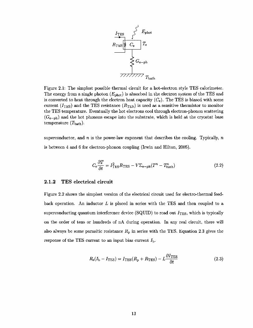
Figure 2.1: The simplest possible therm al circuit for a hot-electron style TES calorimeter.The energy from a single photon (2?phot) is absorbed in the electron system of the TES and is converted to heat through the electron heat capacity (Ce). The TES is biased with some current ( I t e s ) and the TES resistance (Z?t e s ) is used as a sensitive therm istor to monitor the TES temperature. Eventually the hot electrons cool through electron-phonon scattering (Ge-ph) and the hot phonons escape into the substrate, which is held at the cryostat base temperature ( r bath)-
superconductor, and n is the power-law exponent tha t describes the cooling. Typically, n
is between 4 and 6 for electron-phonon coupling (Irwin and Hilton, 2005).
2 .1 .2 T E S electr ica l circu it
Figure 2.2 shows the simplest version of the electrical circuit used for electro-thermal feed-
superconducting quantum interference device (SQUID) to read out / t e s > which is typically
on the order of tens or hundreds of nA during operation. In any real circuit, there will
also always be some parasitic resistance R p in series with the TES. Equation 2.3 gives the
response of the TES current to an input bias current / b.
= ^t e s -Bt b s - V 'S „ -p h ( r " - 7 ? . ,h ) (2.2 )
back operation. An inductor L is placed in series with the TES and then coupled to a
R s{Ib ~ I t e s ) = 1 te s ( jR p + - R t e s ) - L —— (2.3)
13
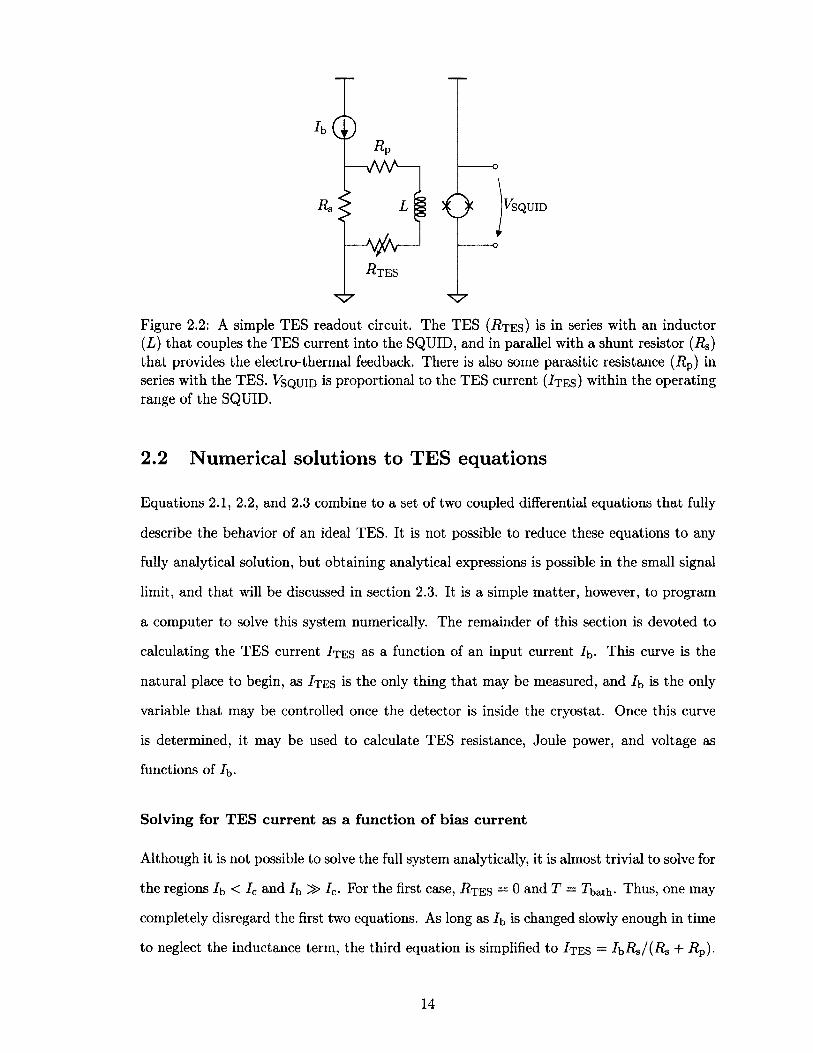
ft®R,
Rs
— AAA-
— M ^ r
R tes
o j^SQUID
Figure 2 .2 : A simple TES readout circuit. The TES ( /? t e s ) is in series with an inductor (L) th a t couples the TES current into the SQUID, and in parallel with a shunt resistor (Rg) tha t provides the electro-thermal feedback. There is also some parasitic resistance (f?p) in series with the TES. Vs q u i d is proportional to the TES current ( / t e s ) within the operating range of the SQUID.
2.2 Num erical solutions to TES equations
Equations 2.1, 2.2, and 2.3 combine to a set of two coupled differential equations tha t fully
describe the behavior of an ideal TES. It is not possible to reduce these equations to any
fully analytical solution, but obtaining analytical expressions is possible in the small signal
limit, and that will be discussed in section 2.3. It is a simple matter, however, to program
a computer to solve this system numerically. The remainder of this section is devoted to
calculating the TES current / t e s a s a function of an input current R. This curve is the
natural place to begin, as / t e s is the only thing tha t may be measured, and R is the only
variable tha t may be controlled once the detector is inside the cryostat. Once this curve
is determined, it may be used to calculate TES resistance, Joule power, and voltage as
functions of R.
Solving for TES current as a function o f bias current
Although it is not possible to solve the full system analytically, it is almost trivial to solve for
the regions R < Ic and R 3 > R. For the first case, /? t e s = 0 and T = Tbath- Thus, one may
completely disregard the first two equations. As long as R is changed slowly enough in time
to neglect the inductance term, the third equation is simplified to / t e s = RRs/(Rs + RP)-
14
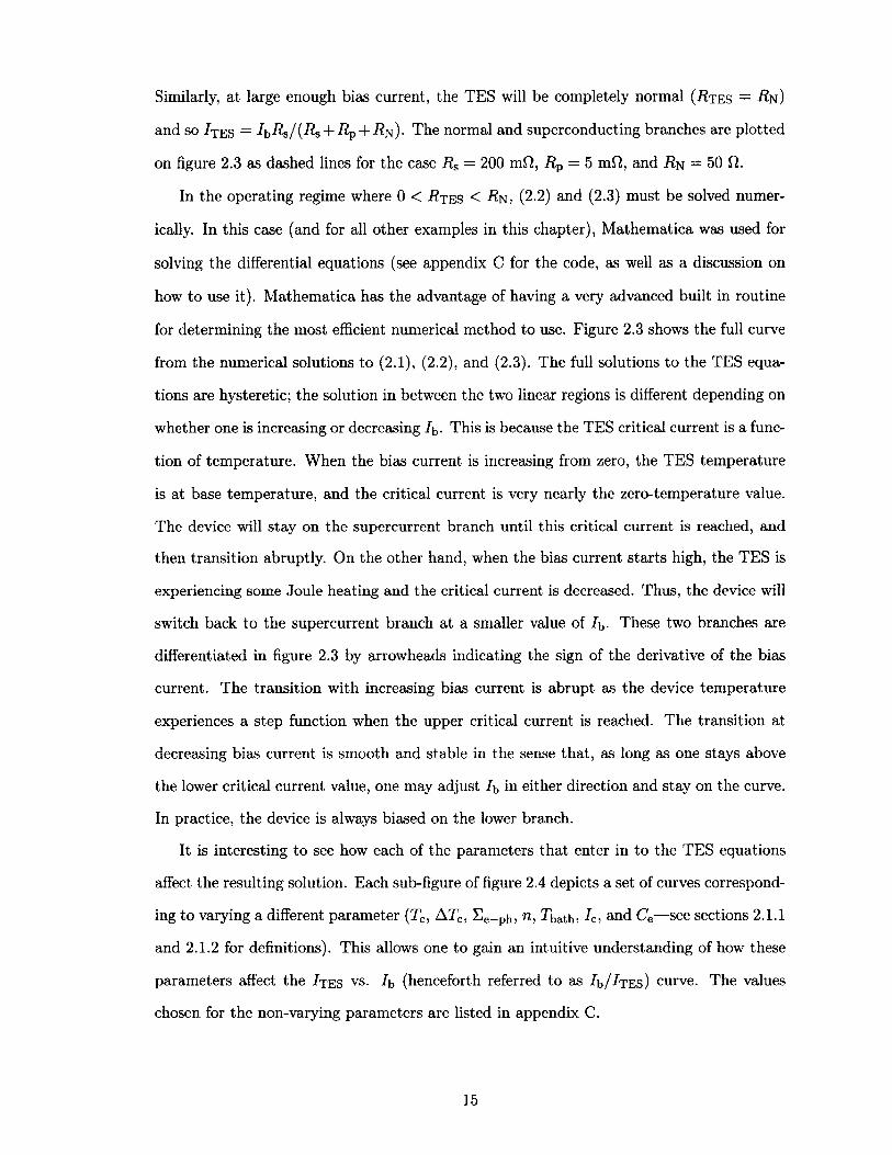
Similarly, at large enough bias current, the TES will be completely normal ( R t e s — R n )
and so / t e s = ^bRs/{Rs + Rp + R n )- The normal and superconducting branches are plotted
on figure 2.3 as dashed lines for the case Rg = 200 mfl, R p — 5 mfl, and i?N = 50 fi.
In the operating regime where 0 < R j e s < R n , (2 .2 ) and (2.3) must be solved numer
ically. In this case (and for all other examples in this chapter), M athematica was used for
solving the differential equations (see appendix C for the code, as well as a discussion on
how to use it). M athematica has the advantage of having a very advanced built in routine
for determining the most efficient numerical method to use. Figure 2.3 shows the full curve
from the numerical solutions to (2 .1 ), (2 .2 ), and (2.3). The full solutions to the TES equa
tions are hysteretic; the solution in between the two linear regions is different depending on
whether one is increasing or decreasing 1^. This is because the TES critical current is a func
tion of temperature. When the bias current is increasing from zero, the TES temperature
is at base temperature, and the critical current is very nearly the zero-temperature value.
The device will stay on the supercurrent branch until this critical current is reached, and
then transition abruptly. On the other hand, when the bias current starts high, the TES is
experiencing some Joule heating and the critical current is decreased. Thus, the device will
switch back to the supercurrent branch at a smaller value of I\>. These two branches are
differentiated in figure 2.3 by arrowheads indicating the sign of the derivative of the bias
current. The transition with increasing bias current is abrupt as the device temperature
experiences a step function when the upper critical current is reached. The transition at
decreasing bias current is smooth and stable in the sense that, as long as one stays above
the lower critical current value, one may adjust /b in either direction and stay on the curve.
In practice, the device is always biased on the lower branch.
It is interesting to see how each of the parameters tha t enter in to the TES equations
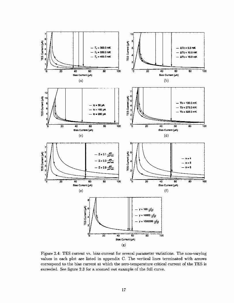
affect the resulting solution. Each sub-figure of figure 2.4 depicts a set of curves correspond
ing to varying a different parameter (Tc, ATC, £ e-ph> n, Tbath) h , and Ce—see sections 2 .1 . 1
and 2.1.2 for definitions). This allows one to gain an intuitive understanding of how these
parameters affect the / t e s vs- /b (henceforth referred to as /b //rE s ) curve. The values
chosen for the non-varying parameters are listed in appendix C.
15
40 60Bias Current (//A)
1 0 0
Figure 2.3: TES current ( / t e s ) vs- bias current ( lb ) numerical solution. Note the hysteresis (denoted by arrows), due to the combination of a temperature-dependent critical current and Joule heating. The dashed gray lines indicate the currents expected for i?TES — 0 and Rtes = R e
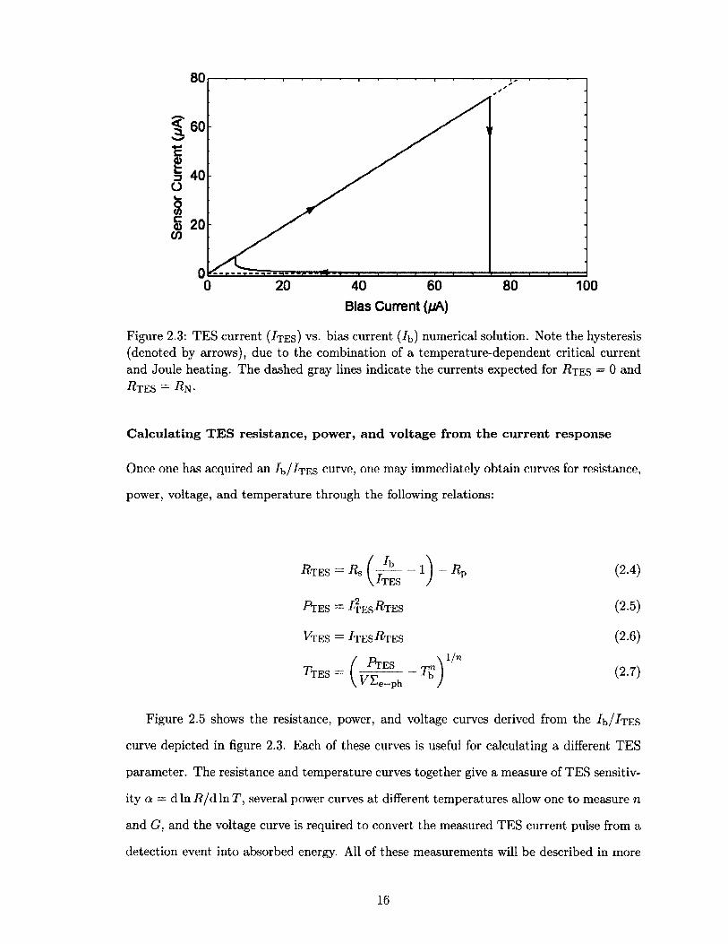
calcula t ing T E S re s is tan c e , pow er, a n d v o ltag e from th e c u r re n t re sp o n se
Once one has acquired an l b / / t e s curve, one may immediately obtain curves for resistance,
power, voltage, and temperature through the following relations:
R tes = Rs ( ^ - i ) - R P (2.4)V t e s /
T ’t e s = Jt e s ^ t e s (2.5)
^TES = Jt ES-Rt ES (2.6)
(2-7)
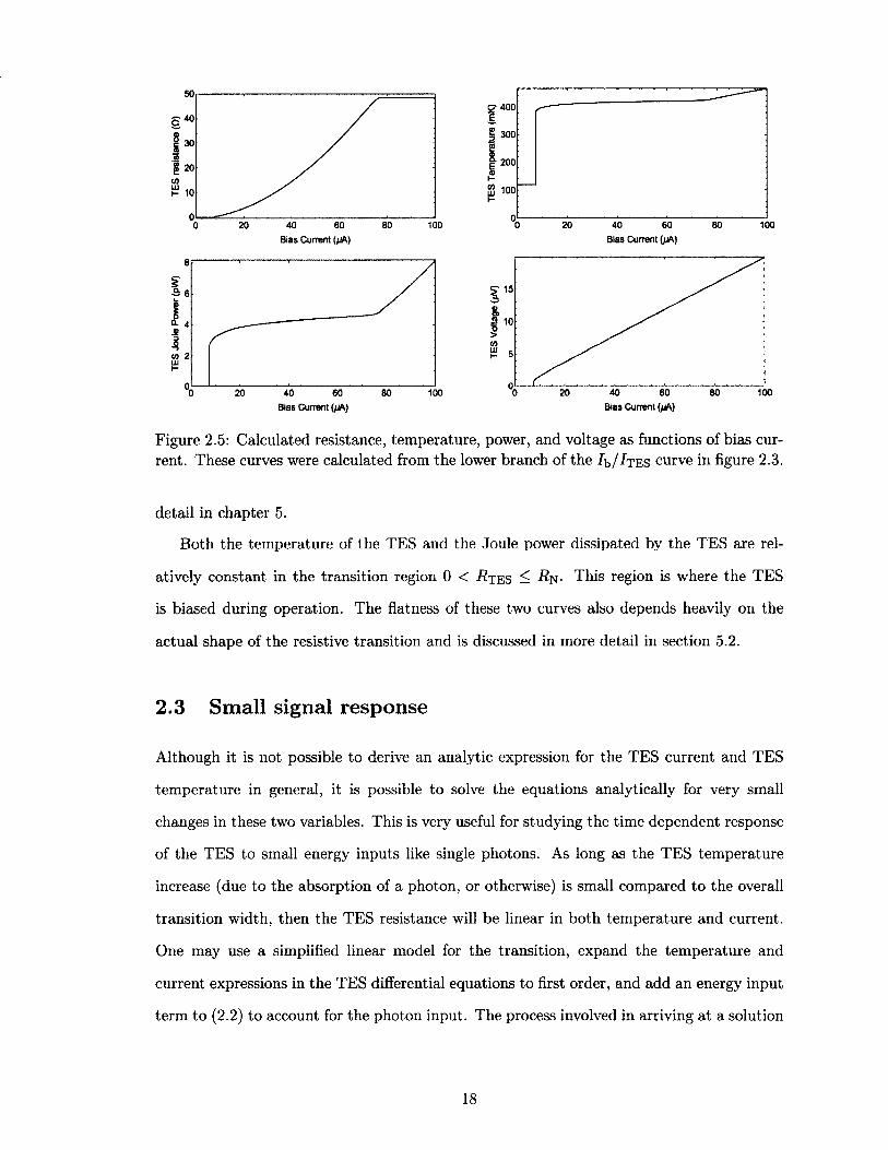
Figure 2.5 shows the resistance, power, and voltage curves derived from the lb / / t e s
curve depicted in figure 2.3. Each of these curves is useful for calculating a different TES
parameter. The resistance and tem perature curves together give a measure of TES sensitiv
ity a = d In R /d ln T , several power curves at different temperatures allow one to measure n
and G , and the voltage curve is required to convert the measured TES current pulse from a
detection event into absorbed energy. All of these measurements will be described in more
16
7
6
I 5— Tc = 300.0 mK
— r c = 350.0 mK
— 7C- 400.0 mK
4
3
2
1
020 40 60 BO 1000
Bias Current (pA)
(a)
ICI3COUJh-
10
8
— ATC = 5.0mK
— ATc - 10.0 mK— ATc = 15.0 mK
6
4
2
0,0 20 40 60 80 100
Bias Current (pA)
(b)
? 10
100Bias Current (pA)
(c)
7SIE 5 E 4
3
2
1
0j 1000 20 40 60 80Bias Current (pA)
(e)
7
laC1 4
— Tb = 100.0 mK
— TO = 275.0 mK— Tb = 325.0 mK3
2
1
0, 20 40 60 80 1000
Bias Current (pA)
(d)
8
0,0 20 40 60 80 100
Bias Current (pA)
( f)
8
-7=10000^- 7 = 1000000^
43mUJi- 2
0,20 40 60 80 1000
Bias Current (pA)
(g)
Figure 2.4: TES current vs. bias current for several parameter variations. The non-varying values in each plot are listed in appendix C. The vertical lines term inated with arrows correspond to the bias current at which the zero-temperature critical current of the TES is exceeded. See figure 2.3 for a zoomed out example of the full curve.
17
I
C- 400
| 300
200
100
10040 60Bias Current (pA)
2 30
" 10
80 100Bias Current (//A)
|©
>WUJ»-
10020Bias Current {fjfs)
100Bias Current (pA)
Figure 2.5: Calculated resistance, temperature, power, and voltage as functions of bias current. These curves were calculated from the lower branch of the Jb/iTES curve in figure 2.3.
detail in chapter 5.
Both the tem perature of the TES and the Joule power dissipated by the TES are rel
atively constant in the transition region 0 < J?tes ^ This region is where the TES
is biased during operation. The flatness of these two curves also depends heavily on the
actual shape of the resistive transition and is discussed in more detail in section 5.2.
2.3 Small signal response
Although it is not possible to derive an analytic expression for the TES current and TES
tem perature in general, it is possible to solve the equations analytically for very small
changes in these two variables. This is very useful for studying the time dependent response
of the TES to small energy inputs like single photons. As long as the TES tem perature
increase (due to the absorption of a photon, or otherwise) is small compared to the overall
transition width, then the TES resistance will be linear in both temperature and current.
One may use a simplified linear model for the transition, expand the tem perature and
current expressions in the TES differential equations to first order, and add an energy input
term to (2.2) to account for the photon input. The process involved in arriving at a solution
18
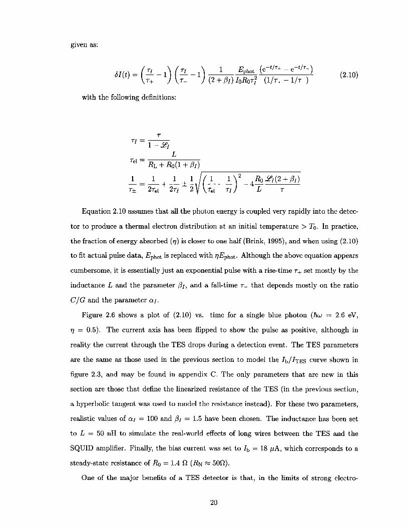
Table 2.1: Definitions of quantities used in the small-signal model described in this section. More details may be found in Irwin and Hilton (2005). In all cases, the subscript “0” indicates an equilibrium value. Ps;g is the signal power, or energy input, term.
SP — Psig - Pq SI = Jt e s -- h ST = T T e s -T o
s v = v h - v Q Oil _ Js l OR - R oW r
IoP i
_ Jxl dR~ Ro HT To
G = n E V T ” - 1 T _ c~ G X i
— T> OC[~ GT0
is beyond the scope of this chapter, but is well documented in extensive detail in Irwin and
Hilton (2005). The following sections will quote and discuss two results of tha t analysis:
the equations for TES response to an incident photon, and the equations describing the
TES noise sources.
2.3 .1 P u lse m od el
The Irwin/Hilton model uses the Thevenin-equivalent circuit for the one depicted in fig
ure 2.2. The bias current and shunt resistor are replaced by a bias voltage V = IbRs and
a load resistor J?l = + Rp in series with the TES and the sense inductor. When the
circuit is held at a constant voltage bias (by supplying an appropriate bias current), the
TES current, temperature, resistance, and power terms may all be expanded about their
equilibrium values (Jo, To, Rq, P q ) to first order. If the input power of a small signal is given
as Psigi then the final linearized equations are given as (2.8) and (2.9) with the definitions
given in table 2 .1 .
d w rl + ro(i + A ) „ se ,G „ ,sv- d t = ------------------ 1 -------------- ~ k L ~ L <2 ' 8 )
w = (29)Q t 0 T O
Solving these two coupled linear equations for SI is tedious, but straightforward. The
response to an incoming photon with energy P photi modeled as a delta-function impulse, is
19
given as:
SI(t \ = ( IL _ A ( iL - i \ I__^Phot (e t/T+ e t/T ) /21Qn{t) ) U ) (2 + 0 j ) I oRot? ( l/r+ - 1 /t_) (2<10)
with the following definitions:
LTel “ R l + R o ( l + 0 t )
1 1 1 1 1 J ( 1 M 2 ^ W + pT)t± 2 re] 2 r j 2 V^ei r j / L r
Equation 2.10 assumes tha t all the photon energy is coupled very rapidly into the detec
tor to produce a thermal electron distribution at an initial temperature > To- In practice,
the fraction of energy absorbed (77) is closer to one half (Brink, 1995), and when using (2.10)
to fit actual pulse data, E phot is replaced with r/Ephot • Although the above equation appears
cumbersome, it is essentially just an exponential pulse with a rise-time r + set mostly by the
inductance L and the parameter 0j, and a fall-time r_ tha t depends mostly on the ratio
C/G and the parameter a / .
Figure 2.6 shows a plot of (2.10) vs. time for a single blue photon {fwj = 2.6 eV,
T} = 0.5). The current axis has been flipped to show the pulse as positive, although in
reality the current through the TES drops during a detection event. The TES parameters
are the same as those used in the previous section to model the /b/^TES curve shown in
figure 2.3, and may be found in appendix C. The only parameters tha t are new in this
section are those tha t define the linearized resistance of the TES (in the previous section,
a hyperbolic tangent was used to model the resistance instead). For these two parameters,
realistic values of aj = 100 and pj = 1.5 have been chosen. The inductance has been set
to L = 50 nH to simulate the real-world effects of long wires between the TES and the
SQUID amplifier. Finally, the bias current was set to 7b = 18 fiA, which corresponds to a
steady-state resistance of i?o = 1.4 fl (7?n ~ 50fi).
One of the major benefits of a TES detector is that, in the limits of strong electro
20
140
120
100<-&m
ill- t>oI
3 4 520 1Time from photon absorption (ps)
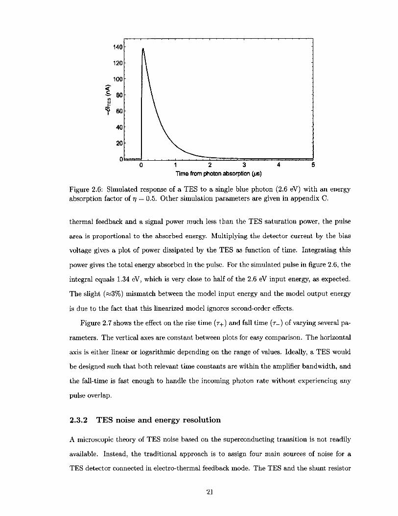
Figure 2.6: Simulated response of a TES to a single blue photon (2.6 eV) with an energy absorption factor of rj — 0.5. Other simulation parameters are given in appendix C.
thermal feedback and a signal power much less than the TES saturation power, the pulse
area is proportional to the absorbed energy. Multiplying the detector current by the bias
voltage gives a plot of power dissipated by the TES as function of time. Integrating this
power gives the total energy absorbed in the pulse. For the simulated pulse in figure 2.6, the
integral equals 1.34 eV, which is very close to half of the 2.6 eV input energy, as expected.
The slight (~3%) mismatch between the model input energy and the model output energy
is due to the fact tha t this linearized model ignores second-order effects.
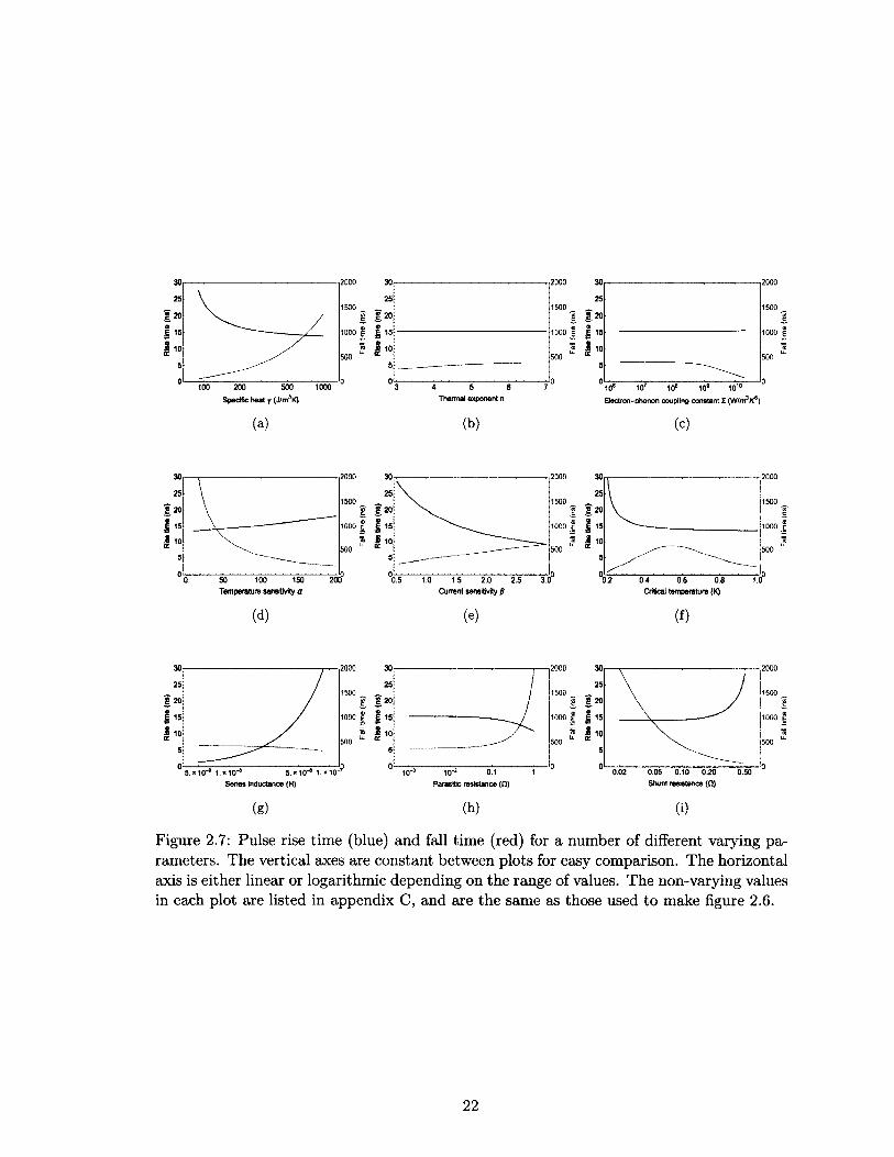
Figure 2.7 shows the effect on the rise time (r+ ) and fall time (r_) of varying several pa
rameters. The vertical axes are constant between plots for easy comparison. The horizontal
axis is either linear or logarithmic depending on the range of values. Ideally, a TES would
be designed such that both relevant time constants are within the amplifier bandwidth, and
the fall-time is fast enough to handle the incoming photon rate without experiencing any
pulse overlap.
2.3 .2 T E S noise and energy reso lu tion
A microscopic theory of TES noise based on the superconducting transition is not readily
available. Instead, the traditional approach is to assign four main sources of noise for a
TES detector connected in electro-thermal feedback mode. The TES and the shunt resistor
21
2000 2000
251500 1500
g 20WC1000 I 1000 i
TOli.
500 500
Thermal exponent n Electron-phonon coupling constant £ (W/m3K*)
2000
251500«e•
IS(£
1000 I
500
100 200 500Specific heat y (J/m3K)
1000
(a) (b) (c)
,2000
1500c_
1 1000 |I 500
02 0.4Critical temperature (K)
0.6
2000
1500«?_c
isa
1000 1
500
0.5 1.5 2.0Current sensitivity 0
301.0 2.5
2000
1500§Iiat
1000 I
500
50 100Temperature sensitivity a
150
(d) (e) (f)
2000 2000 2000
25
? ? 2 0;50Q 1500
g 20 g 20 c
1000 I1000 I
500 11500
10"*
Parasitic resistance (□)0.1 0.02 0.05 0.10 0.20
Shunt resistance (O)0.50
Series inductance (H)
(g) (h) (i)
Figure 2.7: Pulse rise time (blue) and fall time (red) for a number of different varying parameters. The vertical axes are constant between plots for easy comparison. The horizontal axis is either linear or logarithmic depending on the range of values. The non-varying values in each plot are listed in appendix C, and are the same as those used to make figure 2.6.
22
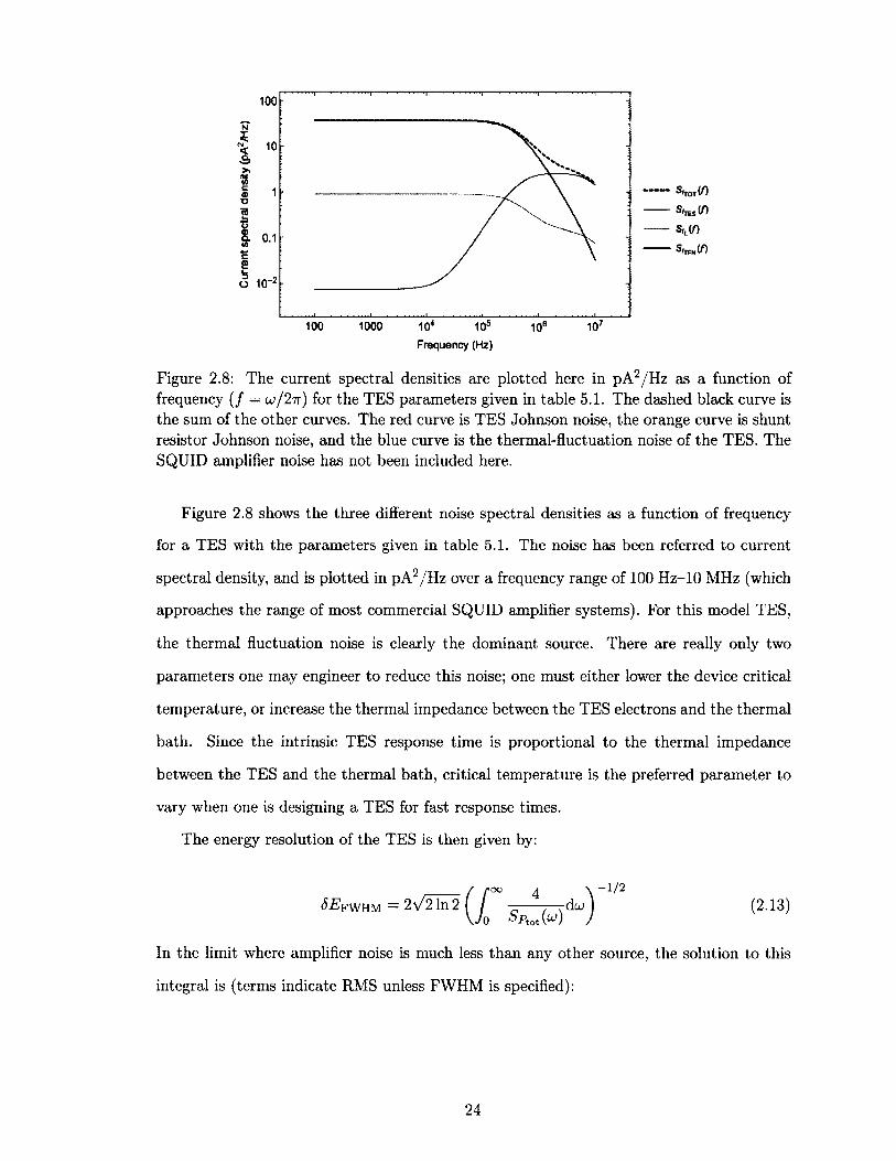
each have Johnson noise. The TES electron system experiences small thermal (energy)
fluctuations, which will be referred to as thermal-fluctuation noise (TFN). Finally, the
SQUID amplifier adds noise. These four noise sources determine the energy resolution of
the detector.
The Johnson noise for the TES and Thevenin-equivalent load resistor follow the typical
Johnson noise formula with voltage spectral density Sy = 4k&TR, which has units of V2 /Hz.
It is im portant to remember, however, tha t R l is at base temperature, while the TES is
approximately at Tc. Thus, SyTE3 = 4A:bTc-Rtes and SyL = 4fcBTbath#L- The thermal noise
formula for power spectral density is similar and is given by SprFN = 4/cqTq G, where G
is the thermal conductance (Mather, 1982) and has units of W 2 /Hz. Finally, the SQUID
amplifier noise is typically quoted as a flux spectral density (5^amp) or current spectral
density (Si ) and must be either measured or acquired from the SQUID manufacturer.
The to tal noise spectral density of the TES is the sum of the four independent noise sources.
In order to perform this sum, the sources must be referred to a common quantity. The two
most useful are current noise (as this is the easiest thing to measure) and power noise, as
the energy resolution is calculated from this quantity. In order to refer a voltage noise to a
power (or current) noise, the voltage to power (or current) responsivity must be calculated.
This is a quantity tha t describes how changes in voltage (as a function of frequency) result in
changes of power (or current). This calculation is complicated, but in the small signal limit
discussed in the previous section, one may arrive at an analytical expression for the total
power-referred TES noise. The details of the calculation, again, are meticulously covered
in Irwin and Hilton (2005).
S p , M = s ^ + Svm i S ^ ( 1 + u V ) + 1 + u 2t?) + ( 2 .1 1 )
All the symbols used are defined in the previous section except for the power to current
responsivity (s/(w)) which is given by:
„ 1 1 ( 1 - r + / r / ) ( 1 - T - / T / )
1 IoRo(2 + 0i) ( l + iair+) (l + iwr_)
23
100
Sitot V)S#Tgs ( 0
sk(f)
100 1000 104 10s 10® 107 Frequency (Hz)
Figure 2.8: The current spectral densities are plotted here in pA2/H z as a function of frequency ( / = for the TES parameters given in table 5.1. The dashed black curve isthe sum of the other curves. The red curve is TES Johnson noise, the orange curve is shunt resistor Johnson noise, and the blue curve is the thermal-fluctuation noise of the TES. The SQUID amplifier noise has not been included here.
for a TES with the parameters given in table 5.1. The noise has been referred to current
spectral density, and is plotted in pA2/H z over a frequency range of 100 Hz-10 MHz (which
approaches the range of most commercial SQUID amplifier systems). For this model TES,
the thermal fluctuation noise is clearly the dominant source. There are really only two
parameters one may engineer to reduce this noise; one must either lower the device critical
temperature, or increase the thermal impedance between the TES electrons and the thermal
bath. Since the intrinsic TES response time is proportional to the thermal impedance
between the TES and the thermal bath, critical temperature is the preferred parameter to
vary when one is designing a TES for fast response times.
The energy resolution of the TES is then given by:
In the limit where amplifier noise is much less than any other source, the solution to this
integral is (terms indicate RMS unless FWHM is specified):
Figure 2.8 shows the three different noise spectral densities as a function of frequency
JEfvvhm = 2 \ / 2 In 2 (2.13)
24
<S2?fwhm = 2 \ / 2 In 2 ~ [(J^f SpTFN + IqSvtes + {■%/ - 1)2IqSvl )
x ( $ S v TES+ l l S v J ] 1/A (2.14)
In the further limits of strong electro-thermal feedback and a base temperature well below
This simplified version, although only strictly true in the above limits, is still a very useful
expression for estimating potential device performance. It captures the strongest predictors
of TES energy resolution: critical temperature, volume (through the heat capacity), the
width of the transition (through the parameter a /) , and the therm al conductance (through
relatively straightforward to engineer. For the example TES tha t has been studied so far in
this chapter, the full-form energy resolution given by (2.14) is <5Ef w h m = 0.08 eV, while the
simplified expression gives 5Efwhm = 0.11 eV. In either case, these numbers are well below
what is actually realized in practice, as they entirely neglect amplifier and environment
noise, but they are a good starting point. In practice, the best detectors measured in the
course of this work had a FWHM energy resolution just over an order of magnitude larger
than the estimate calculated from (2.15).
the critical temperature, the above equation reduces to a much simplified expression:
«5EFWh m = 2 \ / 2 1 n 2 W ^ To C ^ (2.15)
the therm al exponent n). Fortunately, these are all parameters (except for a /) tha t are
25
Experiment design *_/
Chapter
THE experiment was conducted in a custom-designed chamber bolted to the cold stage
of an Oxford Triton cryogen-free dilution refrigerator. The design posed several
technical challenges, which fell into three broad categories:
1. Designing feedthroughs to pass all the electrical lines and the optical fiber from the
vacuum of the cryostat through to the hermetically sealed chamber containing the
superfluid He bath.
2. Filling the experimental chamber with helium.
3. Ensuring tha t the large volume of superfluid never became an inadvertent bomb, by
emptying the chamber sufficiently fast (yet non-destructively) in the case of a rapid
unscheduled warmup.
Figure 3.1 shows a computer rendering of a cross-section of the experimental chamber.
The baseplate and the mounting bracket are machined from oxygen-free high therm al con
ductivity (OFHC) copper. The “L” shaped lid is machined from a solid block of aluminum
and sealed to the baseplate with an indium seal. The chamber contains feedthroughs for
low-voltage signal and amplifier wires, high-voltage wires for biasing the tungsten tip, a
fiber optic line for detector characterization, and ports for filling and venting helium. Each
of these sub-systems is described in this chapter.
Capillary
HV Feedthrough (one of 2)
Tungsten Ground HVNeedle Mesh Mesh
SignalFeedthrough
SQUIDs w/ Nb shielding)
• 10cm
(a) © IEEE 2014
(b)
Figure 3.1: The left panel is a computer render of the experimental chamber and is reprinted with permission from Carter et al. (2014). The right panel shows a photo of the actual experiment.
27
3.1 Helium plumbing
Condensing a large volume of liquid helium into a chamber at the bottom stage of a cryostat
(and keeping it there) is a tricky business. When liquid helium is cooled below 2.2 K, it be
comes a superfluid. Superfluid He has practically zero viscosity and can leak through even
the smallest of holes. This means tha t special care must be taken when joining together
different sections of plumbing, as many standard joints are not superfluid tight. Further
more, superfluid He is essentially a superconductor of heat. This fact, coupled with the
superfluid’s proclivity for climbing walls, means tha t one must take care tha t the bottom
stages of one’s cryostat are not inadvertently thermally shorted together by the superfluid
film. There are three ways to prevent this from happening. One might use a superfluid-
tight valve that is closed once the reservoir has been filled to capacity; one might employ
a so-called film-burner to interrupt the climbing superfluid film either via heat or a very
sharp edge; or one may simply reduce the diameter of the filling tube sufficiently tha t even
when the tube’s walls are fully coated with a superfluid film, it does not present enough
of a heat leak to overwhelm the cooling power available at the cryostat base plate (for a
more in depth discussion of each, see Pobell (2007)). The first option is conceptually the
simplest, however superfluid-tight valves tha t may be remotely actuated are not available
commercially, though Pobell (2007) discusses how to construct such a valve from scratch (it
is not a simple task). The design and manufacture of a good film-burner is one of the few
trade secrets left to manufacturers of dilution refrigerators, which is a good indication of the
difficulty inherent in building one from scratch. Although film burners (or film interrupters)
are conceptually simple (either a small heater to locally heat above 2.2 K or a sharp enough
edge to break the superfluid surface tension), the execution can require a large amount of
either experience or trial and error. For this experiment the third method was employed;
helium is both injected into, and extracted from, the experimental chamber using a thin
stainless steel capillary. In order to avoid ice blockages in the capillary, the helium must be
sufficiently cleaned of impurities before injection. To this end, the room temperature He
gas was circulated through a liquid nitrogen cold trap for several hours prior to injection.
Figure 3.2 depicts the entire fill circuit, both in and out of the cryostat. Appendix B
28

port#2safety k e g tX } - storage keg
inletcontrol
□ 50K
ovcflow metercokJtrap
circulationcontrol
►XJportffl
MC
Figure 3.2: Plumbing diagram for a system designed to handle the ultra-high purity 4 He. See appendix B for operational modes, and the text for description.
details every mode of operation discussed in this chapter.
3.1 .1 P lum b in g inside th e cryostat
A colleague at Yale, Fragner (2013), found through trial and error tha t the optimal inner
diameter of a He fill capillary is around 1 mm. He found tha t diameters below about
0.7 mm were prone to ice blockage, and tha t 1 mm is a good compromise between heat leak
(through the superfluid Rollin film, a r ) 1 and fill time (oc r 4)2. The capillary is heat-sunk
by brazing it into spiral grooves cut into OFHC copper posts, which are then bolted to
each cryostat stage. Because the capillary tubing for this experiment was purchased in five
foot sections, a flange was required to join individual segments. A custom-made, circular,
bolt-together, indium-sealed flange brazed or soldered to the capillary works well for this,
as do the swage-style connectors from HIP3. To connect the capillary to the experimental
chamber in this experiment, a circular indium-sealed flange was used, similar in design to
the one used for joining sections of capillary.
The original design called for a capillary tube from room temperature to base temper
1. For a fixed film thickness, the circumference sets the heat leak.
2. See the Hagen-Poiseuille equation.
3. High Pressure Equipment Company, part number 15-21AF1, http://w w w .highpressure.com .
29
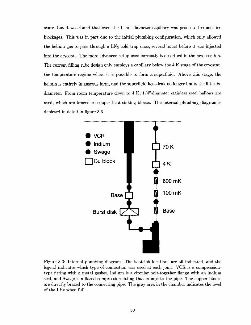
ature, but it was found tha t even the 1 mm diameter capillary was prone to frequent ice
blockages. This was in part due to the initial plumbing configuration, which only allowed
the helium gas to pass through a LN2 cold trap once, several hours before it was injected
into the cryostat. The more advanced setup used currently is described in the next section.
The current filling tube design only employs a capillary below the 4 K stage of the cryostat,
the tem perature regime where it is possible to form a superfluid. Above this stage, the
helium is entirely in gaseous form, and the superfluid heat-leak no longer limits the fill-tube
diameter. Prom room temperature down to 4 K, l /4 ”-diameter stainless steel bellows are
used, which are brazed to copper heat-sinking blocks. The internal plumbing diagram is
depicted in detail in figure 3.3.
■ rI] 70 K
n 4 K
1 600 mK
I 100 mK
1 Base
Figure 3.3: Internal plumbing diagram. The heatsink locations are all indicated, and the legend indicates which type of connection was used a t each joint: VCR is a compression- type fitting with a metal gasket, Indium is a circular bolt-together flange with an indium seal, and Swage is a flared compression fitting tha t crimps to the pipe. The copper blocks are directly brazed to the connecting pipe. The gray area in the chamber indicates the level of the LHe when full.
# VCR# Indium# Swage
I | Cu block
Base
Burst disk
30
To fill the chamber, a 50 L volume of isotopically pure 4He (less than 1 part in 1012
3 He; obtained from the research group of Peter McClintock, Lancaster University, UK)
gas pressurized to 2 bar (100 L at STP) is opened to the capillary through an adjustable
impedance when the cryostat baseplate reaches 4 K. The reason the helium is not opened
to the capillary at once is because the optical fiber feedthrough (see section 3.5) does not
become sufficiently vacuum tight until well below 70 K and it is undesirable to leak helium
gas into the cryostat vacuum space. The adjustable impedance is used to keep the injection
pressure below about 20 Torr. This limits the heat load and keeps the dilution refrigerator
from entering into an unstable mode of operation. He gas is subsequently cryo-pumped
into the fill lines and eventually condensed into the chamber as the cryostat cools to base
temperature. During this process, the impedance is continually adjusted (opened more and
more) to keep the injection pressure constant.
To empty the chamber, heat is slowly applied to boil the liquid helium back into the
50 L gas storage vessel through the capillary. During this process, the compressor is used
to keep the pressure at the top of the capillary low. This fully-closed system is useful for
two reasons: no liquid level measure is required as a known quantity of gas is used, and as
it is a closed system, no helium is lost. This second point is crucial, as isotopically pure
4He is very expensive!
In the event of an ice blockage in the capillary or a rapid warm-up event due to cryostat
failure, the capillary may prove incapable of emptying the chamber fast enough to avoid
dangerous pressures (helium has a liquid-to-gas expansion ratio of s»750). To allow for the
emergency decompression of the chamber, a large-diameter path from the chamber to an
evacuated 50 L volume at room tem perature was constructed. This emergency relief path
was sealed from the chamber with a 3 bar burst-disk4 at the cold stage to contain the su
perfluid. To accommodate the thermally expanding gas while minimizing the stainless steel
thermal link, the burst line is constructed from a welded series of thin-walled tubes ( 1 0 mil) 5
of increasing diameter towards warmer stages to accommodate the gas expansion. Thermal
4. Oseco, h ttp://w w w .oseco.com /.
5. Vita Needle Company, h t tp : / /v i t a n e e d le . com.
31
baffles inside the burst line shield the cold stages from blackbody radiation emanating from
the warmer stages. The burst line connects to the chamber using a VCR fitting, and to
a room temperature stainless steel bellows using a special metal O-ring6. The addition of
the burst line did not add a significant heat load to the base-plate of the cryostat, and
only raised the base tem perature from 15 mK to about 25 mK. It did, however, make the
cryostat tem perature more susceptible to building vibrations produced by large air handlers
on the top floor.
3.1.2 Plumbing outside the cryostat
The external plumbing system must accomplish three goals. It must be able to circulate the
He through a cold trap in a closed cycle prior to filling, to remove air contamination; it must
be able to both fill and empty the chamber; and it must be able to recover any He vented in
the case of a burst-disk rupture. These goals are accomplished with a circulator pump, two
off-the-shelf 50 L beer kegs (purchased clean and new for this experiment), two nitrogen
cold-traps, and a menagerie of valves, gauges, and kwik-flange (KF) hardware. One beer
keg is used as the fill volume, and one is kept at vacuum for collecting any helium tha t vents
through the burst-disk during a failure. Beer kegs are cheaper than any vacuum/pressure
vessel that is sold explicitly for scientific work and they also ship food-grade clean. To attach
the kegs to the vacuum system, KF507 flanges were welded to them. Figure 3.2 shows the
pumping circuit and highlights the different modes of operation, and figure 3.4 shows the
beer kegs mounted overhead the experiment. Because most of the external plumbing uses
compression joints with rubber O-rings tha t are not UHV leak-tight, the He is passed
through a second cold trap right before it enters the internal fill lines in the cryostat. All
the plumbing between the final cold-trap and the internal fill lines utilizes metal-to-metal
UHV seals to prevent any air contamination tha t could result in an ice blockage. In order
to evenly circulate the helium through the cold trap from a keg with only one opening, a
small-diameter length of Cu pipe was inserted through the neck of the fill keg to the bottom;
6. Kurt J. Lesker Company, h ttp : //le sk e r .c o m .
7. Kurt J. Lesker Company, h ttp : //le sk e r .c o m .
32
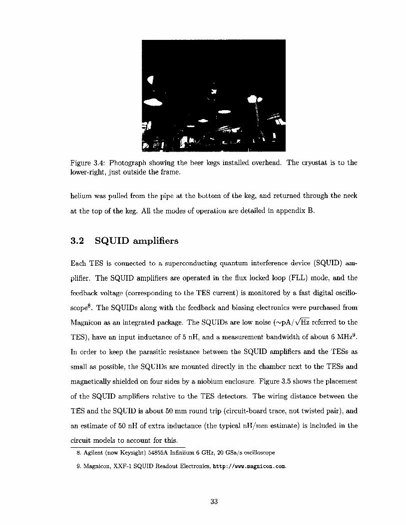
Figure 3.4: Photograph showing the beer kegs installed overhead. The cryostat is to the lower-right, just outside the frame.
helium was pulled from the pipe at the bottom of the keg, and returned through the neck
at the top of the keg. All the modes of operation are detailed in appendix B.
3.2 SQUID amplifiers
Each TES is connected to a superconducting quantum interference device (SQUID) am
plifier. The SQUID amplifiers are operated in the flux locked loop (FLL) mode, and the
feedback voltage (corresponding to the TES current) is monitored by a fast digital oscillo
scope8. The SQUIDs along with the feedback and biasing electronics were purchased from
Magnicon as an integrated package. The SQUIDs are low noise (~pA/v^Hz referred to the
TES), have an input inductance of 5 nH, and a measurement bandwidth of about 6 MHz9.
In order to keep the parasitic resistance between the SQUID amplifiers and the TESs as
small as possible, the SQUIDs are mounted directly in the chamber next to the TESs and
magnetically shielded on four sides by a niobium enclosure. Figure 3.5 shows the placement
of the SQUID amplifiers relative to the TES detectors. The wiring distance between the
TES and the SQUID is about 50 mm round trip (circuit-board trace, not twisted pair), and
an estimate of 50 nH of extra inductance (the typical nH/m m estimate) is included in the
circuit models to account for this.
8. Agilent (now Keysight) 54855A Infiniium 6 GHz, 20 GSa/s oscilloscope
9. Magnicon, XXF-1 SQUID Readout Electronics, http://www.magnicon.com.
33
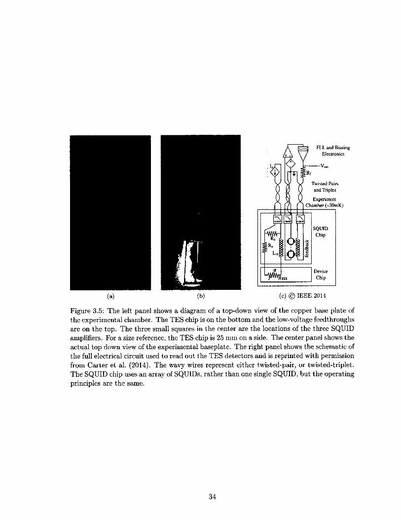
FLL and Biasing Electronics
—Vo„,
Twisted Pairs and Triples
Experiment amber (~30mK)
SQUIDChip
Device Chip
(a) (b) (c) © IEEE 2014
Figure 3.5: The left panel shows a diagram of a top-down view of the copper base plate of the experimental chamber. The TES chip is on the bottom and the low-voltage feedthroughs are on the top. The three small squares in the center are the locations of the three SQUID amplifiers. For a size reference, the TES chip is 25 mm on a side. The center panel shows the actual top down view of the experimental baseplate. The right panel shows the schematic of the full electrical circuit used to read out the TES detectors and is reprinted with permission from Carter et al. (2014). The wavy wires represent either twisted-pair, or twisted-triplet. The SQUID chip uses an array of SQUIDs, rather than one single SQUID, but the operating principles are the same.
34
3.3 Low voltage wiring
Each of the three SQUID amplifier channels requires seven wires. In addition to these
signal wires, extra wiring was installed for general use (thermometry, level sensing, heaters,
etc). Copper wire was used from room temperature to 4 K, and NbTi wire from 4 K to
base temperature. All 48 wires were assembled into two flat ribbon cables, which were heat
sunk at each stage and fed into the superfluid volume through two 25-pin micro-D hermetic
flanges10, which were laser welded into a circular flange and bolted to the chamber with an
indium seal.
3.4 High voltage electronics and wiring
Although the ionization potential of He is large, it is possible to create He^ excimers through
electron discharge from a sharp needle. To maximize electric field (and minimize the re
quired voltage), a tungsten needle was fabricated with a « 1 0 0 nm tip radius following a
sodium-hydroxide etch recipe published by Golov and Ishimoto (1998) (see figure 3.6). A
metallic mesh connected to ground was placed just after the needle to collect the electrons
em itted from the tip. Figure 3.6 shows the basic circuit diagram for the tip, as well as a
photograph of the circuit installed in the chamber.
To access the tip and grid, GPO thread-in hermetic feedthroughs11 were used. They
are both resilient at high voltage (up to about 2 kV) and are superfluid-tight when the
supplied rubber O-ring is replaced with an indium seal. The HV lines used the same wire
as the low-voltage ribbon cables, but with the addition of insulating teflon sleeves. Custom
designed heatsinking clamps for each stage were used to thermally anchor the HV lines
without shorting them electrically, by counteracting the necessarily thick insulating layers
with a large contact area (figure 3.7).
Initially, the high voltage for the tip was to be supplied by small switched-mode pro-
10. SRI Hermetics Inc., Part number SRIMD505-25-B, h ttp ://w w .sr ih e r m e tic s .c o m . The Ceramax proprietary ceramic forms a superfluid-tight seal between each beryllium-copper pin and the surrounding stainless steel body.
11. Corning Gilbert, part number 0119-783-1, h ttp ://co rn in g .co m .
35
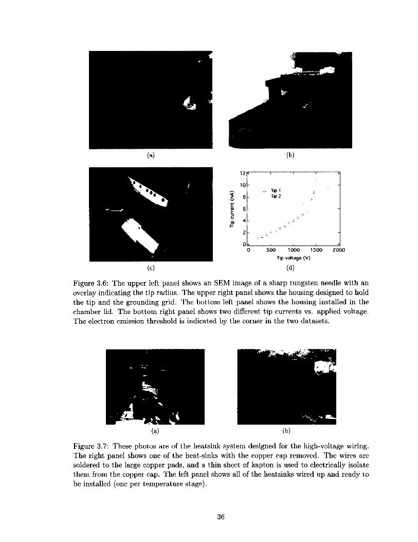
(a) (b)
-r
s
12 * ------- ,--------- j------ -- j---- ... ^
10 -
A Tip 1<C 8 - Tip 2 -*•*4)H 6 - -C3Q. 4 - -P
2 - -
0 t l I I .....t0 500 1000 1500 2000
Tip voltage (V)(c) (d)
Figure 3.6: The upper left panel shows an SEM image of a sharp tungsten needle with an overlay indicating the tip radius. The upper right panel shows the housing designed to hold the tip and the grounding grid. The bottom left panel shows the housing installed in the chamber lid. The bottom right panel shows two different tip currents vs. applied voltage. The electron emission threshold is indicated by the corner in the two datasets.
(a) (b)
Figure 3.7: These photos are of the heatsink system designed for the high-voltage wiring. The right panel shows one of the heat-sinks with the copper cap removed. The wires are soldered to the large copper pads, and a thin sheet of kapton is used to electrically isolate them from the copper cap. The left panel shows all of the heatsinks wired up and ready to be installed (one per temperature stage).
36

grammable DC-DC converters12 tha t take an input of 0-5 V and output 0-1000 V. This
small power supply was wired in series with a fast DC-DC amplifier tha t can output short
pulses (~ fis) of a few hundred volts. This configuration was intended to hold the tip just
below the He ionization threshold and then momentarily push it over and realize a pulse of
He?; excimers. However, there were two reasons this setup was abandoned. The first is that,
contrary to expectations (Guo et al. (2009) achieved excimer creation with only 400 V),
the voltage required at the tip to create excimers was more than 1700 V. This was greater
than the intended supply could output. Secondly the small power supplies were very noisy
at the switching frequency (~ 100 kHz), which is right in the middle of the measurement
bandwidth. A low-pass filter bank was added according to methods described in a tech
nical note published by Crane Aerospace (2006), but it was not enough to damp out the
interference completely.
Eventually, a commercial high-voltage power supply capable of outputting 5000 V was
used13. It was necessary to float it using a ground-isolating plug. The internal capacitance
of the supply was very high and so, when coupled to the large resistance of the tip/grid
circuit, the maximum response time was on the order of several seconds. This made pulsed
operation impossible. Instead, the supply was simply set to a voltage such tha t the detector
experienced an event rate of ~1 Hz.
3.5 Fiber optics
It is useful to have an optical fiber mounted directly over the TES detectors in order to
characterize them with photons of a known energy. To this end, a multi-mode fiber with
a 300 pm diameter1 4 was suspended a few cm above the TES chip. The fiber entered the
cryostat through a hermetic seal at room tem perature15. No attem pt was made to heat-sink
the fiber, and the base temperature of the dilution refrigerator was insensitive to whether
12. American Power, part number M5-S1000, h ttp ://h ttp ://a p o w e rd esig n .c o m /.
13. Stanford Research Systems, part number PS350, http://w w w .th inksrs.com .
14. ThorLabs, part number FT300UMT, h ttp ://w w w .thorlab s.com /.
15. Ocean Optics, part number VFT-400-UV-16, h ttp ://w w w .ocean optics.com /.
37
or not the fiber was installed. The fiber entered the chamber through a superfluid-tight
feedthrough, which was created following the procedure of Butterworth et al. (1998). In this
method the seal is made through the thermal contraction of a length of heat-shrink tubing 1 6
during cool down. Although this feedthrough was not He leak-tight at room temperature,
it worked very well when cold, and was thermally cycled many times successfully. It was
also, however, very fragile. A small accidental bump was often enough of a disturbance
to require rebuilding of the feedthrough; this occurred several times. Finally, it was not
resilient to a high pressure difference. A pressure of even 300 mBar inside of the chamber
with the cryostat at vacuum and the baseplate at 4 K was enough to destroy the seal.
16. TE Connectivity, part number MFT-MT1000-N0.2-X-SP, h ttp ://w w w .te .com /. Several brands and types of heat shrink tubing were investigated. The part listed above is the only one that tested superfluid- leak-tight.
38
TES design and fabrication
Chapter
De s i g n i n g a detector is an exercise in compromises. The materials used and the
physical shape are not only defined by what physical characteristics are desired
(heat capacity, collection area, critical temperature, etc...), but also by what fabrication
processing is available and how complex a process one is willing to undertake. The resulting
design used in this experiment was a titanium TES with aluminum leads, which was then,
in some cases, coated with a thin layer of either gold or platinum. This chapter starts with
a discussion of the desired operating characteristics tha t are required of a detector. This is
followed by a discussion of what materials and fabrication processes were available. Finally,
a description is given of the steps used to fabricate the detectors. All the detectors were
fabricated at Yale by the author.
The critical temperature of pure Al is about 1.2 K, so if Al is used as an absorber, the
detector TES must have a lower Tc, preferably by a factor of three or more in order to
efficiently trap quasiparticles in the TES. For a TES held near TCTES, the number of quasi
particles above the Al gap tha t may escape is described by a Boltzmann distribution and
is oc exp(—A/&bTct e s ), where the superconducting energy gap A = l .75ksT^1 (Bardeen
4.1 TES materials
et al., 1957). For r rA1/7 ’(,TES > 3, the Boltzmann factor is < 10-2 . Also, the sensitivity
of a TES improves with decreasing critical temperature, so the lower the Tc of the TES
in general, the better. Although it is common to achieve a low Tc by combining a bilayer
of a normal metal and a superconductor, the added fabrication and engineering challenges
involved in tuning the bilayer properties ruled out tha t approach for this work. There are
only a few natural superconductors tha t may be reliably produced in thin-films, tha t have a
low enough critical temperature to trap quasiparticles, and have a high enough critical tem
perature to operate above ~50 mK in a dilution refrigerator; they are uranium (U), hafnium
(Hf), tungsten (W), titanium (Ti), and iridium (Ir), and each will be discussed separately.
One thing tha t will not be considered here is the coupling of triplet state excimers to the
TES surface. The mechanism for this is highly dependent on the surface density of states
of the TES, which may altered at will by depositing a very thin layer of some other metal
(or oxide) on top of the TES. This is discussed more in chapter 7.
Uranium
Uranium has a Tc of 200 mK, which would be perfect if it weren’t for the two facts that
uranium is highly radioactive and one of the most controlled materials in the world.
Iridium
Iridium has a bulk Tc of about 100 mK. Iridium does not tarnish or oxidize. From a fab
rication perspective, this is very appealing, as one may deposit a layer of Ir, process that
layer in atmosphere, and deposit another layer of metal onto the processed Ir without wor
rying about the formation of an oxide tunnel barrier. Iridium may be either evaporated or
sputtered, although successful evaporation requires ultra-high vacuum and a heated sub
strate (Irwin and Hilton, 2005). Iridium is easily RF sputtered to achieve a thin film with
a Tc of 120 mK (Bogorin and Galeazzi, 2008), and tha t process has been meticulously doc
umented by Bogorin (2008). Iridium has two drawbacks. The first is tha t it can suffer
from phase separation (where the material is partially normal and partially superconduct
ing) when used as a calorimeter due to its low thermal conductivity and this can result in
non-uniform phase across the TES, which negatively affects the response (Fukuda, 2002).
40
The second, and more important, is that Ir is extremely expensive. Since Yale lacks the
facilities to properly evaporate Ir, it would have to be sputtered. Sputtering targets are
very wasteful in the sense that once they are used up, there is still a large amount of metal
left over. In the end, the high expense of Ir is what removed it from consideration as a
detector material.
Tungsten
Tungsten has a phase-dependent critical temperature. The a-phase has a Tc of about
15 mK, and the ,3-phase Tc is between 1 K and 4 K. Thin film W is typically a mixture of
the two phases depending on deposition parameters, and may be tuned to exhibit either a
pure phase or some mixture of the two. Lita et al. (2005) have characterized how the Tc
of sputtered W varies with sputtering power and pressure. Tungsten has a much higher
thermal conductivity than Ir and therefore does not suffer from the phase-separation issue
as much. For these reasons, W was the initial choice for making the sensors. However,
despite several attem pts over some months, obtaining sputtered W with a Tc above 20 mK
proved to be untenable. After several discussions with the authors of Lita et al. (2005),
it became clear tha t the failure to successfully sputter W was due to two reasons. The
sputtering chamber at Yale does not have the ability to heat the substrate, and the wafers
were coated in PMMA e-beam resist (to pattern the W using a lift-off process), which out-
gassed during deposition and affected the resultant W phase. In order to achieve a good
phase mixture, and therefore an appropriate Tc, the sputtering chamber must be absolutely
clean; the outgassing of the PMMA was sufficient to derail the process entirely. In fact, Lita
found tha t even sputtering a different metal in the same sputtering chamber was sufficient
to force any W sputtered in the same chamber into the a phase. For these reasons, it was
decided to abandon the idea of a tungsten TES.
Hafnium
Hafnium has a critical temperature around 120 mK and has been used successfully for
TESs (Lita et al., 2009). It is also relatively inexpensive (compared to Ir). However, after
several unsuccessful months attempting to engineer W thin-films tha t were acceptable for
41
TES fabrication, the decision to avoid trying to characterize another new material was
made. Instead, Ti was chosen as it was readily available in an evaporator and already well
characterized at Yale.
Titanium
Titanium has a bulk Tc of about 400 mK. It is easily evaporated onto a room temperature
substrate and the quality of the vacuum in the evaporator does not seem to influence the
Tc very much. Although 400 mK is a little higher than the ideal temperature of ~100 mK,
the advantages of using Ti for these initial studies far outweighed the disadvantage for Ti of
losing some signal due to incomplete quasiparticle trapping. Additionally, Yale has an evap
oration chamber tha t has both Ti and Al targets, which means a bilayer may be deposited
without breaking vacuum, ensuring very good contact between metals. Furthermore, Ti
devices created with the same evaporation chamber have been well characterized in prior
years (Santavicca et al., 2009, 2010). The Tc of Ti is also tunable (in general) by combining
the Ti with a thick layer of normal metal and using the proximity effect to lower the Tc (Ven
tu ra et al., 2002). This was not attem pted however, as this work was meant as a proof of
concept rather than a best-possible-implementation. In retrospect, the 400 mK transition
tem perature was somewhat advantageous for studying the dynamics of He^ excimers as,
near the end of the experiment, a malfunctioning air-handler in the building dramatically
increased the mechanical vibrations of the cryostat, raising the base temperature to nearly
100 mK.
4.2 Fabrication
All devices discussed in this dissertation were fabricated on bare (unoxidized) high-resistivity
silicon wafers1. All the metal depositions were accomplished using electron beam evapo
ration in a commercial evaporator from Plasma Systems2. The patterning was done using
electron-beam lithography in a Raith EBPG 5000+ system. In Chapter 5 several configura
1. Crystec, (100) oriented, 500 /um thick, single-side polished, 2 inch Si wafers with resistivity > 10 kflcm
2. Plassys UMS300 UHV, h ttp : //p la ssy s .c o m
42
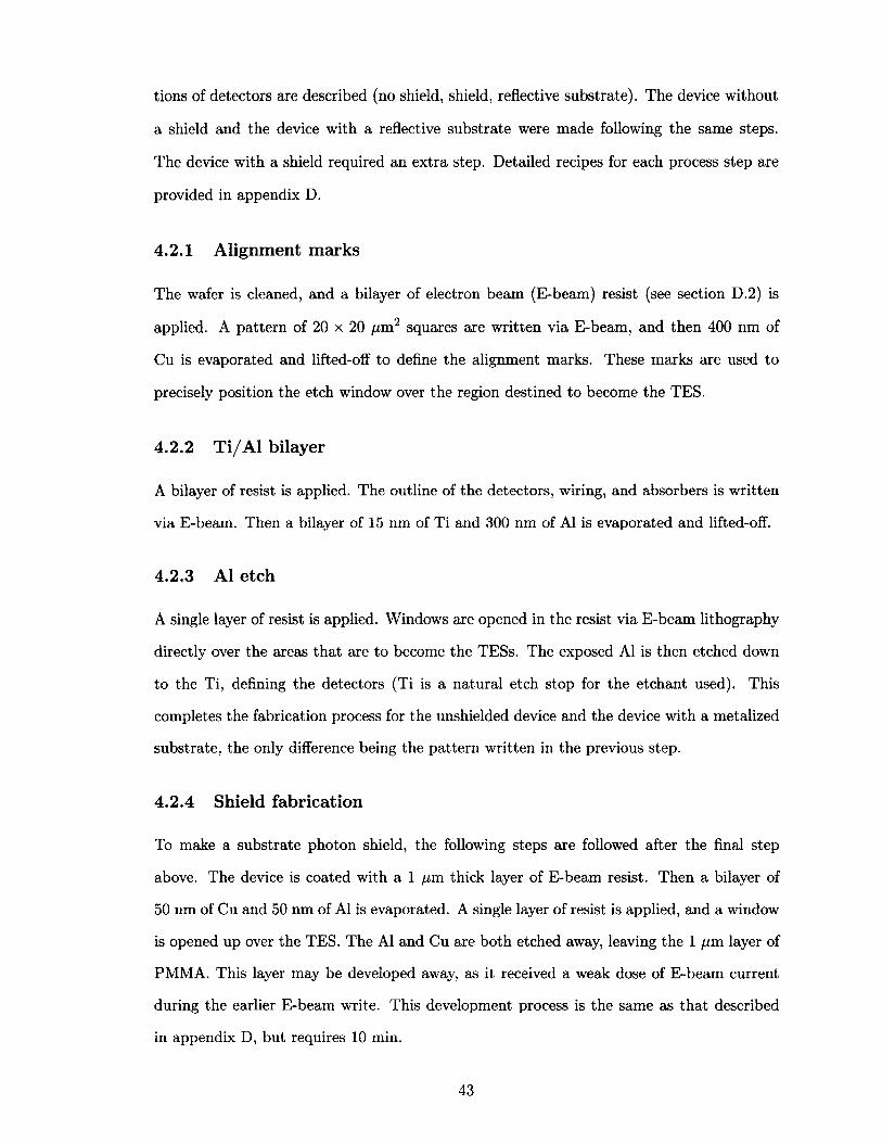
tions of detectors are described (no shield, shield, reflective substrate). The device without
a shield and the device with a reflective substrate were made following the same steps.
The device with a shield required an extra step. Detailed recipes for each process step are
provided in appendix D.
4.2 .1 A lign m en t m arks
The wafer is cleaned, and a bilayer of electron beam (E-beam) resist (see section D.2) is
applied. A pattern of 20 x 20 ptm2 squares are written via E-beam, and then 400 nm of
Cu is evaporated and lifted-off to define the alignment marks. These marks are used to
precisely position the etch window over the region destined to become the TES.
4 .2 .2 T i /A l bilayer
A bilayer of resist is applied. The outline of the detectors, wiring, and absorbers is written
via E-beam. Then a bilayer of 15 nm of Ti and 300 nm of Al is evaporated and lifted-off.
4 .2 .3 A l etch
A single layer of resist is applied. Windows are opened in the resist via E-beam lithography
directly over the areas tha t are to become the TESs. The exposed Al is then etched down
to the Ti, defining the detectors (Ti is a natural etch stop for the etchant used). This
completes the fabrication process for the unshielded device and the device with a metalized
substrate, the only difference being the pattern written in the previous step.
4 .2 .4 Sh ield fabrication
To make a substrate photon shield, the following steps are followed after the final step
above. The device is coated with a 1 pm thick layer of E-beam resist. Then a bilayer of
50 nm of Cu and 50 nm of Al is evaporated. A single layer of resist is applied, and a window
is opened up over the TES. The Al and Cu are both etched away, leaving the 1 pm layer of
PMMA. This layer may be developed away, as it received a weak dose of E-beam current
during the earlier E-beam write. This development process is the same as tha t described
in appendix D, but requires 10 min.
43
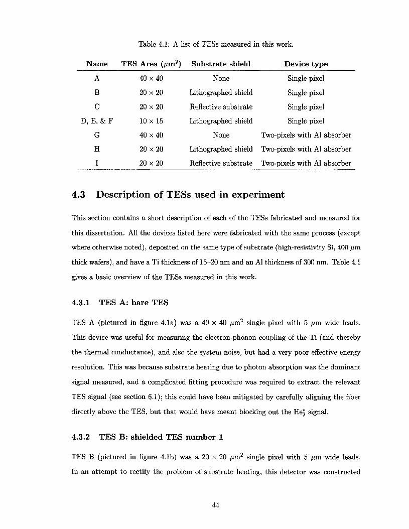
Table 4.1: A list of TESs measured in this work.
Name TES Area (/mi2) Substrate shield Device type
A 40 x 40 None Single pixel
B 2 0 x 2 0 Lithographed shield Single pixel
C 2 0 x 2 0 Reflective substrate Single pixel
D, E, & F 10 x 15 Lithographed shield Single pixel
G 40 x 40 None Two-pixels with Al absorber
H 2 0 x 2 0 Lithographed shield Two-pixels with Al absorber
I 2 0 x 2 0 Reflective substrate Two-pixels with Al absorber
4.3 Description of TESs used in experim ent
This section contains a short description of each of the TESs fabricated and measured for
this dissertation. All the devices listed here were fabricated with the same process (except
where otherwise noted), deposited on the same type of substrate (high-resistivity Si, 400 /im
thick wafers), and have a Ti thickness of 15-20 nm and an Al thickness of 300 nm. Table 4.1
gives a basic overview of the TESs measured in this work.
4.3 .1 T E S A: bare T ES
TES A (pictured in figure 4.1a) was a 40 x 40 yum2 single pixel with 5 /an wide leads.
This device was useful for measuring the electron-phonon coupling of the Ti (and thereby
the therm al conductance), and also the system noise, but had a very poor effective energy
resolution. This was because substrate heating due to photon absorption was the dominant
signal measured, and a complicated fitting procedure was required to extract the relevant
TES signal (see section 6.1); this could have been mitigated by carefully aligning the fiber
directly above the TES, but tha t would have meant blocking out the He^ signal.
4 .3 .2 T E S B: sh ielded T ES num ber 1
TES B (pictured in figure 4.1b) was a 20 x 20 /zm2 single pixel with 5 yum wide leads.
In an attem pt to rectify the problem of substrate heating, this detector was constructed
44
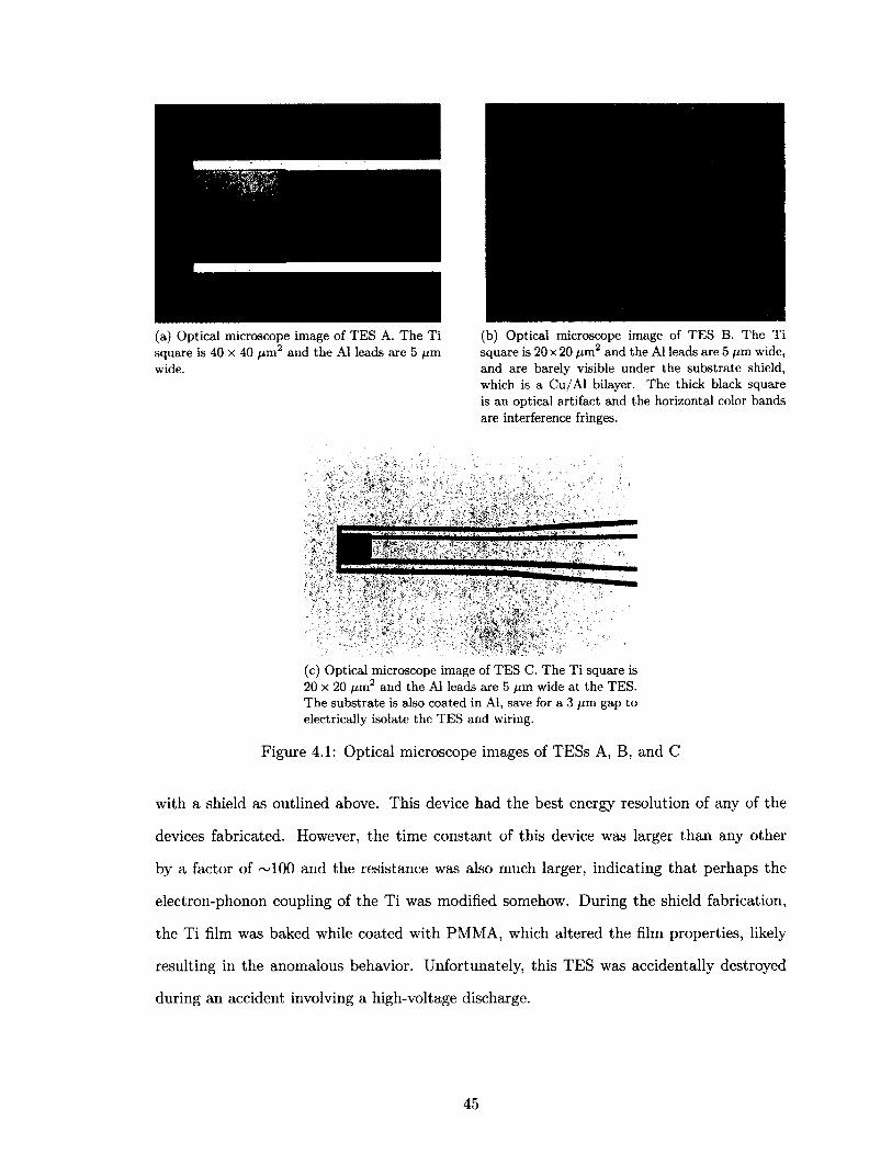
(a) Optical microscope image of TES A. The Ti square is 40 x 40 /rm2 and the Al leads are 5 /irn wide.
(b) Optical microscope image of TES B. The Ti square is 20 x 20 /im2 and the Al leads are 5 fim wide, and are barely visible under the substrate shield, which is a C u/Al bilayer. The thick black square is an optical artifact and the horizontal color bands are interference fringes.
(c) Optical microscope image of TES C. The Ti square is 20 x 20 ^m2 and the Al leads are 5 fim wide at the TES.The substrate is also coated in Al, save for a 3 fim gap to electrically isolate the TES and wiring.
Figure 4.1: Optical microscope images of TESs A, B, and C
with a shield as outlined above. This device had the best energy resolution of any of the
devices fabricated. However, the time constant of this device was larger than any other
by a factor of ~ 1 0 0 and the resistance was also much larger, indicating tha t perhaps the
electron-phonon coupling of the Ti was modified somehow. During the shield fabrication,
the Ti film was baked while coated with PMMA, which altered the film properties, likely
resulting in the anomalous behavior. Unfortunately, this TES was accidentally destroyed
during an accident involving a high-voltage discharge.
45

4 .3 .3 T E S C: T E S w ith reflective su b strate
TES C (pictured in figure 4.1c) was a 20 x 20 /xm2 single pixel with 5 /im wide leads. This
TES was fabricated without a shield. Instead of a metallic shield on a layer of PMMA, the
substrate of this device was coated entirely in aluminum except for a small ~ 2 yum wide
channel surrounding the device to keep it electrically isolated. The intent of the design was
tha t any photons incident on the substrate would reflect, rather than be absorbed. This
TES had a similar time constant and similar resistivity to TES A. The device performance
was much better than TES A, but a substrate contribution to the signal was still observed.
This was the first TES tha t was immersed in superfluid helium, and also the first TES
to detect the excimer signal. However, the performance was not nearly as good as either
TES B or TES D.
4 .3 .4 T E S D , E, and F: sh ield ed T E S num ber 2
TES D (pictured in figure 4.2) was a 10 x 15 yum2 single pixel with 5 yum wide leads. This
TES was fabricated with a substrate shield, but in a slightly different way from TES B.
Instead of performing the aluminum etch tha t exposed the Ti surface before the PMMA
shield spacer was added, this Al etch was performed last, after the shield had been added;
essentially the final two fabrication steps outlined above were swapped. This reordering of
steps was so tha t the Al would protect the Ti surface from contamination from the PMMA
during the shield fabrication. This TES had similar resistivity and similar time constants
to TESs A and C, indicating tha t the altered fabrication recipe protected the Ti. The
energy resolution was still not as good as TES B, but it was sufficient to resolve single blue
photons. This TES (along with TESs E and F) was used to take all the helium excimer
data described in chapter 7.
TESs E and F were identical to TES D, save for an extra layer of sputtered metal
coating the detector. TES E was coated with 10-20 nm of gold, and TES F was coated
with 10-20 nm of platinum. These thicknesses are estimates based on past sputter-tool
performance and were not measured. The Ti surfaces were not cleaned in any way prior to
the sputter coating.
46
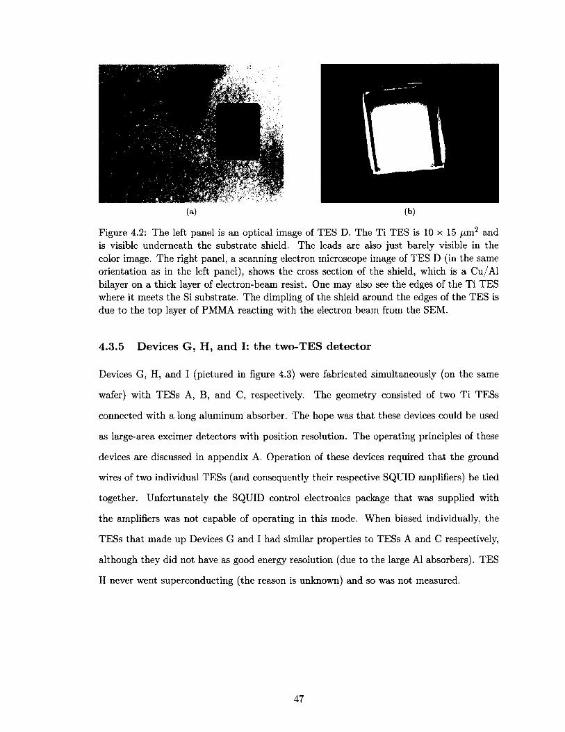
(a) (b)
Figure 4.2: The left panel is an optical image of TES D. The Ti TES is 10 x 15 fim 2 and is visible underneath the substrate shield. The leads are also just barely visible in the color image. The right panel, a scanning electron microscope image of TES D (in the same orientation as in the left panel), shows the cross section of the shield, which is a Cu/Al bilayer on a thick layer of electron-beam resist. One may also see the edges of the Ti TES where it meets the Si substrate. The dimpling of the shield around the edges of the TES is due to the top layer of PMMA reacting with the electron beam from the SEM.
4.3 .5 D ev ices G , H , and I: th e tw o-T E S d etector
Devices G, H, and I (pictured in figure 4.3) were fabricated simultaneously (on the same
wafer) with TESs A, B, and C, respectively. The geometry consisted of two Ti TESs
connected with a long aluminum absorber. The hope was tha t these devices could be used
as large-area excimer detectors with position resolution. The operating principles of these
devices are discussed in appendix A. Operation of these devices required tha t the ground
wires of two individual TESs (and consequently their respective SQUID amplifiers) be tied
together. Unfortunately the SQUID control electronics package that was supplied with
the amplifiers was not capable of operating in this mode. When biased individually, the
TESs tha t made up Devices G and I had similar properties to TESs A and C respectively,
although they did not have as good energy resolution (due to the large Al absorbers). TES
H never went superconducting (the reason is unknown) and so was not measured.
47
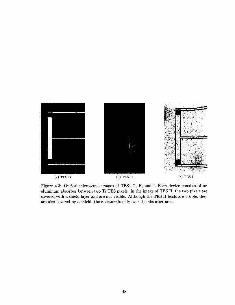
(a) TES G (b) TES H (c) TES I
Figure 4.3: Optical microscope images of TESs G, H, and I. Each device consists of an aluminum absorber between two Ti TES pixels. In the image of TES H, the two pixels are covered with a shield layer and are not visible. Although the TES H leads are visible, they are also covered by a shield; the aperture is only over the absorber area.
48
Detector characterization 5
Chapter
HIS chapter consists of two main parts. The first several sections describe how various
TES parameters may be measured and presents some measurements from the devices
described in section 4.3. The final section discusses the basics of photon detection. In
practice, for single-photon detection, a careful calibration of all the TES parameters is
not really necessary. This is because any device tha t is sensitive to single-photons is self-
calibrating through fitting the response histogram of the TES (to a known energy source)
with a Poisson distribution—a process described in section 5.5 and chapter 6 . For this
reason, not all the devices used in this experiment were exhaustively characterized. At least
one example of each type of measurement is given in this chapter, but they are not all
necessarily of the same TES.
Ideally, the characterization of a TES detector would simply consist of measuring every
single param eter listed in chapter 2. At this point, one could appeal to the small-signal pulse
model (discussed in section 2.3) to create a model pulse response to an incoming photon, use
this model to construct an optimal filter template, and then be done with characterization
and calibration in one fell swoop. Unfortunately, some parameters are harder to measure
than others, and not all may be directly measured while the TES is wired in the electro
thermal feedback circuit. An example of two such parameters are the sensitivities of the
resistance to temperature (a /) and to TES current (/?/). These are difficult to measure
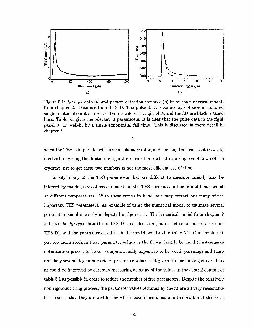
3 6
100 150 2000 50
0.12
0.10
0.08
'Z 0.06
0.02
0.000 2 4 6 B 10
Bias currant (/rA) Time from trigger (f/s)
(a) (b)
Figure 5.1: /b/^TES data (a) and photon-detection response (b) fit by the numerical models from chapter 2. D ata are from TES D. The pulse data is an average of several hundred single-photon absorption events. D ata is colored in light blue, and the fits are black, dashed lines. Table 5.1 gives the relevant fit parameters. It is clear tha t the pulse data in the right panel is not well-fit by a single exponential fall time. This is discussed in more detail in chapter 6
when the TES is in parallel with a small shunt resistor, and the long time constant (~week)
involved in cycling the dilution refrigerator means tha t dedicating a single cool-down of the
cryostat just to get these two numbers is not the most efficient use of time.
Luckily, many of the TES parameters tha t are difficult to measure directly may be
inferred by making several measurements of the TES current as a function of bias current
at different temperatures. W ith these curves in hand, one may extract out many of the
im portant TES parameters. An example of using the numerical model to estimate several
parameters simultaneously is depicted in figure 5.1. The numerical model from chapter 2
is fit to the /b/^TES data (from TES D) and also to a photon-detection pulse (also from
TES D), and the parameters used to fit the model are listed in table 5.1. One should not
put too much stock in these parameter values as the fit was largely by hand (least-squares
optimization proved to be too computationally expensive to be worth pursuing) and there
are likely several degenerate sets of parameter values that give a similar-looking curve. This
fit could be improved by carefully measuring as many of the values in the central column of
table 5.1 as possible in order to reduce the number of free parameters. Despite the relatively
non-rigorous fitting process, the parameter values returned by the fit are all very reasonable
in the sense tha t they are well in line with measurements made in this work and also with
50
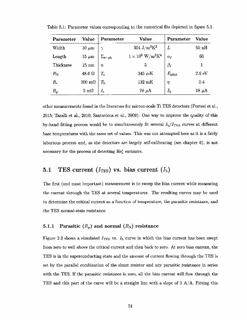
Table 5.1: Parameter values corresponding to the numerical fits depicted in figure 5.1.
Parameter Value Parameter Value Parameter Value
W idth 1 0 pm 7 304 J / m 3 K 2 L 50 nH
Length 15 pm ^e—ph 1 x 10⁹ W /m 3 Kn a i 60
Thickness 15 nm n 5 01 1
i?N 48.6 Q Tc 345 mK -Lphot 2.6 eV
Rs 2 0 0 mfl Tb 132 mK V 0.4
R p 5 mQ Ic 70 pA lb 18 pA
other measurements found in the literature for micron-scale Ti TES detectors (Portesi et al.,
2015; Taralli et al., 2010; Santavicca et al., 2009). One way to improve the quality of this
by-hand fitting process would be to simultaneously fit several Jb//rES curves at different
base temperatures with the same set of values. This was not attem pted here as it is a fairly
laborious process and, as the detectors are largely self-calibrating (see chapter 6 ), is not
necessary for the process of detecting He^ excimers.
5.1 TES current ( / t e s ) v s . bias current (4 )
The first (and most important) measurement is to sweep the bias current while measuring
the current through the TES at several temperatures. The resulting curves may be used
to determine the critical current as a function of temperature, the parasitic resistance, and
the TES normal-state resistance.
5.1.1 Parasitic (Rp) and normal (jRn) resistance
Figure 2.3 shows a simulated / t e s vs. Jb curve in which the bias current has been swept
from zero to well above the critical current and then back to zero. At zero bias current, the
TES is in the superconducting state and the amount of current flowing through the TES is
set by the parallel combination of the shunt resistor and any parasitic resistance in series
with the TES. If the parasitic resistance is zero, all the bias current will flow through the
TES and this part of the curve will be a straight line with a slope of 1 A /A . Fitting this
51
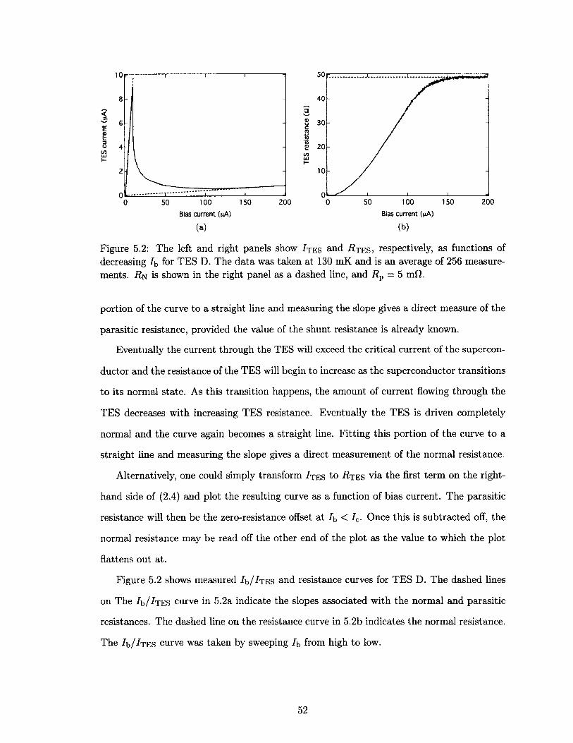
5 0 p
40
o'ucroto(A<u
2000 50 1 0 0 150
10
8
6
4
2
01 0 0 150 2000 50
Bias current (|iA) Bias current (nA)
(a) (b )
Figure 5.2: The left and right panels show / t e s and R t e s > respectively, as functions of decreasing I\> for TES D. The data was taken at 130 mK and is an average of 256 measurements. i?N is shown in the right panel as a dashed line, and R p = 5 mO.
portion of the curve to a straight line and measuring the slope gives a direct measure of the
parasitic resistance, provided the value of the shunt resistance is already known.
Eventually the current through the TES will exceed the critical current of the supercon
ductor and the resistance of the TES will begin to increase as the superconductor transitions
to its normal state. As this transition happens, the amount of current flowing through the
TES decreases with increasing TES resistance. Eventually the TES is driven completely
normal and the curve again becomes a straight line. Fitting this portion of the curve to a
straight line and measuring the slope gives a direct measurement of the normal resistance.
Alternatively, one could simply transform / t e s to R j e s via the first term on the right-
hand side of (2.4) and plot the resulting curve as a function of bias current. The parasitic
resistance will then be the zero-resistance offset at /b < / c- Once this is subtracted off, the
normal resistance may be read off the other end of the plot as the value to which the plot
flattens out at.
Figure 5.2 shows measured /b //rE S and resistance curves for TES D. The dashed lines
on The /b//TES curve in 5.2a indicate the slopes associated with the normal and parasitic
resistances. The dashed line on the resistance curve in 5.2b indicates the normal resistance.
The /b//TES curve was taken by sweeping /b from high to low.
52
5.1 .2 C ritical current (Ic) and critica l tem p eratu re (Tc)
There is some hysteresis of the critical current because the critical current is a function of
temperature; a device tha t is warm from Joule heating will have a lower critical current
than a device tha t is fully superconducting and at base temperature. The critical current
measured as lb is increased can be recorded at several temperatures and the resulting curve
may be fit to the Ginzburg-Landau relation I(T) = Jc( l - T /T c ) 3 / 2 and used to extract
the zero-temperature critical current Jc and the zero-current critical tem perature Tc. It is
entirely possible tha t the Ginzburg-Landau relationship will not fit the data well as it is
based on the assumption of a perfectly homogeneous one-dimensional superconductor and
is only valid near Tc. If this is the case, trial and error may be used to find a better fit
function, and this fit function may be used in (2 .1 ) to make a better model of the resistive
transition vs. current.
5.2 TES Joule power ( P t e s ) v s- bias current ( J b )
The Joule power is given by (2.5). Ideally Ptes as a function of bias current will be zero
while the TES is superconducting, some constant value while the device is held on the
transition and the electro-thermal feedback perfectly balances the input and output power,
and then quadratic in Jb once the TES is driven fully normal. There are two major reasons
why a TES might exhibit a behavior in the transition region tha t deviates from the expected
constant value.
1 . A TES may experience phase separation during the superconducting transition. Typ
ically, a TES should transition smoothly from being all superconducting to all normal
as it is heated. However, it is possible tha t instead it can separate into multiple spa
tial regions tha t have slightly different transition temperatures and critical currents.
This effectively turns the TES into multiple TESs in series and the effect on the Joule
power curve is the introduction of a number of steps into the region tha t should be
smooth. Phase separation happens when the internal thermal conductance of the
TES (typically dominated by electron-electron interaction and electron diffusion) is
53
sufficiently lower than the dominant cooling mechanism (electron-phonon interaction)
tha t regions of the TES cool into the substrate faster than the TES can equilibrate.
2. It is also possible for the “constant” power region of the P j curve to have a uniform
slope. The slope of this portion of the curve is a measure of the width (in temperature)
of the superconducting transition.
In practice, both of these effects may be present with different contribution strengths. The
power curves depicted in figure 5.3b, from TES A, exhibit one step-like feature as well as
a region tha t has a uniform slope. This suggests tha t the TES is experiencing some minor
phase separation, but it still has a large linear section tha t is fairly wide in temperature.
The simple thermal model from chapter 2 would require a more complicated equation to
accurately model these power curves. Compare these to the power curve measured from
TES D in figure 5.3d. Although the curve from TES D has a slope in the bias region, it is
very smooth with no kinks or steps, indicating tha t there is no phase separation present.
This is not surprising since TES D is much smaller than TES A.
The TES power vs. bias current curve may be used to infer values for thermal conduc
tance as well as the exponent, n, tha t determines the power-law for TES cooling.
5.2 .1 T herm al con d u ctan ce (G e- Ph) and th erm al exp on en t (n )
The thermal conductance may be measured indirectly by measuring the TES Joule power
at a fixed bias current at a number of different bath temperatures. In steady state operation
(2 .2 ) becomes / | es 1 ?tes = P t e s = F E e-p h (T cn — T £ ) . A plot is then made of P t e s v s . Tb
and the above power law is fit to the data, allowing n and Ee- Ph to vary. G is the derivative
of the power law and is given by G = n F £ e-p h lc"_1 .
Figure 5.3 shows bias curves at three temperatures and their associated calculated TES
power curves from TES A. Figure 5.3c shows the steady state power as a function of
temperature for two different bias points (indicated by dashed gray lines on the power
plot). Each data-point on the third panel corresponds to an /b/^TES curve taken at a
different cryostat temperature; only three are shown in the first two panels for clarity. The
fits give values for K = Ee_phF and n. Note tha t at different bias points the values for
54
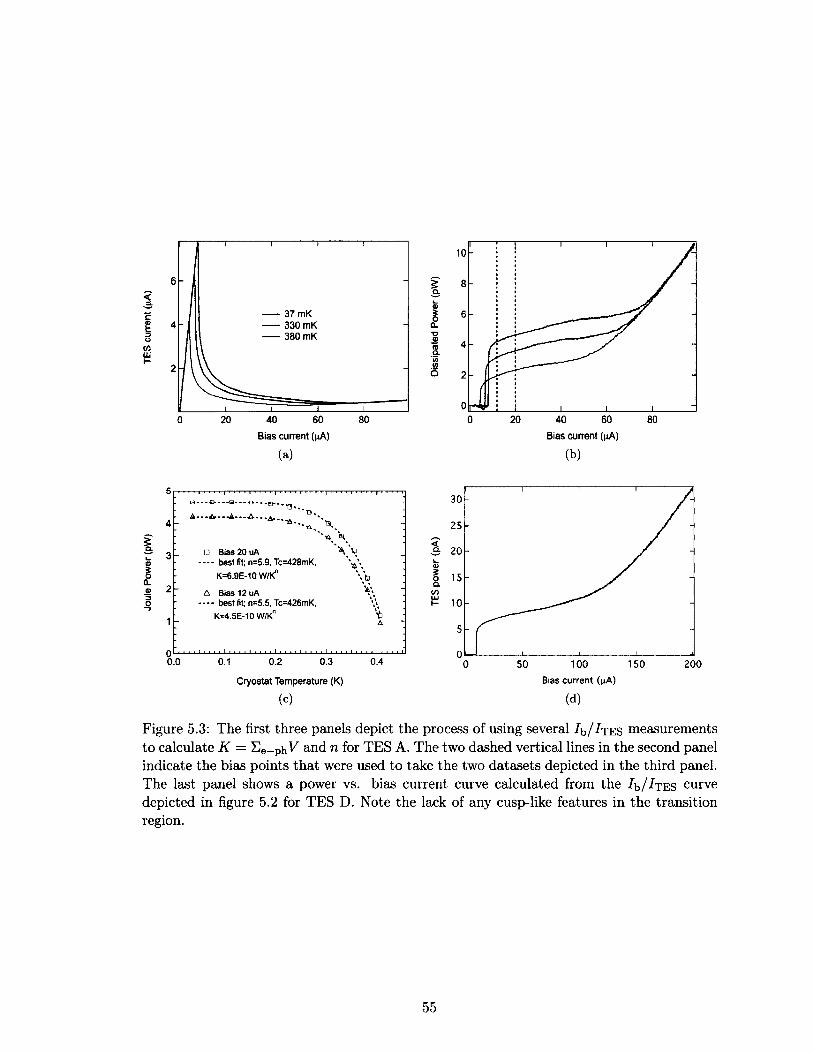
toLUI-
6
37 mK 330 mK 380 mK
4
2
40 60 800 20
Bias current (|iA)
(a)
5Q.
IOCL
aQ
10
8
6
4
2
0
60 800 20 40Bias current (uA)
(b)
ICLa
00.0
i ' i I 1
: A— A . ^ 'T3-.: X -
A. \1 □ Bias 20 uA..................best fit; n=5.9, Tc=428mK, V\
K=6.9E-10W/Kn W7 A Bias 12 uA %*\
. . . . best fit; n=5.5, Tc=426mK,\^ K=4.5E-10W/Kn
'................... i ................. .. i . . * i . . .
A
1L4..LL.L.LLI ..lie 1 10.1 0.2 0.3
Cryostat Temperature (K)
(c)
0.4
<3 20k_VI 15Q.10inK 10
50 1 0 0 150 2000
Bias current (jiA)
(d)
Figure 5.3: The first three panels depict the process of using several ib/TrES measurements to calculate K = S e- PhF and n for TES A. The two dashed vertical lines in the second panel indicate the bias points tha t were used to take the two datasets depicted in the third panel. The last panel shows a power vs. bias current curve calculated from the /b/^TES curve depicted in figure 5.2 for TES D. Note the lack of any cusp-like features in the transition region.
55

thermal conductance and n are slightly different. It is also interesting to note that, for
TES A (see figure 5.3b), there appears to be a cusp in what should be the smooth linear
region of each power curve. As discussed earlier in this section, it is likely tha t this TES,
which was the largest one measured, was experiencing a small amount of phase separation.
For comparison, the power curve from TES D, depicted in figure 5.3d, does not contain
any cusp-like features. Throughout the course of this experiment, TES A was the only
subject of an attem pt to measure £ e- Ph and n as the values from the fits in figure 5.3 are
in reasonably good agreement with values measured by Wei et al. (2008).
For a TES tha t cools predominately through electron-phonon coupling in the supercon
ductor n — 5 is the value predicted by theory for a pure metal (Irwin and Hilton, 2005).
However, a range of values of n may be reasonably expected for the two following reasons:
1. Measurements of n can be highly dependent on the device resistance. As an example,
Lindeman et al. (2008) report tha t using the same method used here, they found values
of n ranging from 2 to 8 for the same system (a T i/A u TES on a SiN membrane),
depending on which resistance they chose to measure at. When they developed a
more accurate method, they found tha t n = 3 for their system (as would be expected
for a system tha t cools predominantly through phonon-phonon interactions).
2. Sergeev and Mitin (2000) calculate an expected range of n between 4 and 6 for electron-
phonon coupling depending on film disorder. Gershenson et al. (2001) report values
of n between 4 and 6 for Hf and Ti films. Wei et al. (2008) also report values of n
between 4 and 6 for Ti TESs.
Another way to arrive at a value for G is to measure the power spectral-density of the
TES as a function of temperature. This is difficult and was not attem pted. If the thermal-
fluctuation noise dominates over the amplifier noise, then the equations in section 2.3.2
may be used to infer the TES thermal conductance. On the other hand, if the amplifier
noise dominates, a good measurement of G may be used to subtract out the thermal-
fluctuation noise contribution to the power spectral-density and get a reasonable estimate
of environmental and amplifier noise contributions.
56
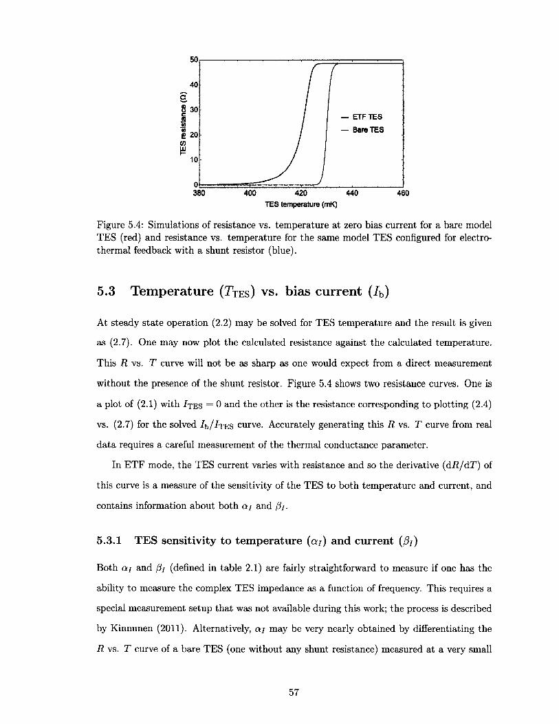
3 30— ETFTES
— Bare TES
3 8 0 4 0 0 420 440 460
TES temperature (mK)
Figure 5.4: Simulations of resistance vs. temperature at zero bias current for a bare model TES (red) and resistance vs. tem perature for the same model TES configured for electrothermal feedback with a shunt resistor (blue).
5.3 Temperature ( T t e s ) v s . bias current ( J b )
At steady state operation (2.2) may be solved for TES temperature and the result is given
as (2.7). One may now plot the calculated resistance against the calculated temperature.
This R vs. T curve will not be as sharp as one would expect from a direct measurement
without the presence of the shunt resistor. Figure 5.4 shows two resistance curves. One is
a plot of (2.1) with / t e s = 0 and the other is the resistance corresponding to plotting (2.4)
vs. (2.7) for the solved R / I tes curve. Accurately generating this R vs. T curve from real
data requires a careful measurement of the thermal conductance parameter.
In ETF mode, the TES current varies with resistance and so the derivative (d R /d T ) of
this curve is a measure of the sensitivity of the TES to both temperature and current, and
contains information about both a j and ,3/.
5.3.1 T E S sen sit iv ity to tem p eratu re (a /) and current (ft/)
Both o lj and /3j (defined in table 2.1) are fairly straightforward to measure if one has the
ability to measure the complex TES impedance as a function of frequency. This requires a
special measurement setup tha t was not available during this work; the process is described
by Kinnunen (2011). Alternatively, a j may be very nearly obtained by differentiating the
R vs. T curve of a bare TES (one without any shunt resistance) measured at a very small
57
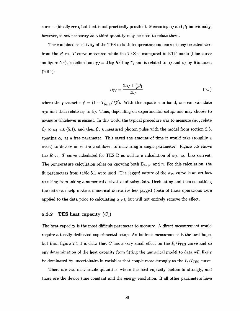
current (ideally zero, but tha t is not practically possible). Measuring a j and 0i individually,
however, is not necessary as a third quantity may be used to relate them.
The combined sensitivity of the TES to both temperature and current may be calculated
from the R vs. T curve measured while the TES is configured in ETF mode (blue curve
on figure 5.4), is defined as a iv = d lo g / i/d log T, and is related to a / and by Kinnunen
(2011):
2“ ' + ? A“ IV = 2 f t ( 5 -1)
where the param eter <j> — (1 — T^ath/T cn). W ith this equation in hand, one can calculate
a iv and then relate a / to (3j. Thus, depending on experimental setup, one may choose to
measure whichever is easiest. In this work, the typical procedure was to measure a iv , relate
/3/ to a / via (5.1), and then fit a measured photon pulse with the model from section 2.3,
treating a / as a free parameter. This saved the amount of time it would take (roughly a
week) to devote an entire cool-down to measuring a single parameter. Figure 5.5 shows
the R vs. T curve calculated for TES D as well as a calculation of a iv vs. bias current.
The temperature calculation relies on knowing both Ee_ph and n. For this calculation, the
fit parameters from table 5.1 were used. The jagged nature of the a iv curve is an artifact
resulting from taking a numerical derivative of noisy data. Decimating and then smoothing
the data can help make a numerical derivative less jagged (both of those operations were
applied to the data prior to calculating a iv ), but will not entirely remove the effect.
5.3 .2 T E S heat cap acity (C e)
The heat capacity is the most difficult param eter to measure. A direct measurement would
require a totally dedicated experimental setup. An indirect measurement is the best hope,
but from figure 2.4 it is clear tha t C has a very small effect on the R / / t e s curve and so
any determination of the heat capacity from fitting the numerical model to data will likely
be dominated by uncertainties in variables tha t couple more strongly to the R / / t e s curve.
There are two measurable quantities where the heat capacity factors in strongly, and
those are the device time constant and the energy resolution. If all other parameters have
58
40
sQ) Ucn■Mt/>U)£
C /5UJH
200 250 300 350 400
40
JS3JJ(0u
0 50 1 0 0 150 200Bias current (pA) Calculated TES tem perature (mK)
(a) (b)
Figure 5.5: Calculated cqv plotted against bias current for TES D (a). Calculated temperature plotted against measured resistance for TES D (b). The temperature was calculated according to (2.7). Values for Ee-ph and n were taken from table 5.1.
been carefully measured, the heat capacity may be determined by fitting a TES pulse with
the model from section 2.3, and treating C as a free parameter. If (as previously mentioned)
aj is also being treated as a free parameter, this task is somewhat more difficult, as both
quantities affect the TES fall-time strongly. One possible option (that was not explored in
this work) is to bias the TES detector in such a way tha t the operating resistance of the TES
is equal to the shunt resistance. In this configuration, the electro-thermal feedback should
be zero, and the TES time constant will be the intrinsic time constant r = C/G. Finally,
if the thermal noise is the dominant system noise contribution, then the measured energy
resolution could be used to calculate C. However, from (2.15) it is clear tha t this method has
the same difficulty as using the time constant; the energy resolution also depends strongly
on Oii. For the purposes of this experiment, it was decided to use the value measured by
Taralli et al. (2010) for evaporated Ti on Si, which is very near the book value.
5.4 TES noise
Section 2.3.2 discusses the dominant noise sources in a TES. Figure 5.6 depicts the measured
current noise for TES A (green trace). The other traces are the calculated curves for the
three dominant TES noise sources: Johnson noise in the TES and in the shunt resistor (blue
curves), and thermal fluctuation noise in the TES (red curve). The SQUID noise quoted by
59
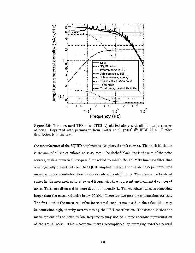
NX>N<CL
</)C<D
"D15k_■MoQ)CL( 0
0 >T>a
86
4-
8 -
6 -
4-
2 -
Q.E 0.1< 8 h
_i t i i i i <
DataSQUID noise Preamp noise in FLL Johnson noise, TES Johnson noise, Rj + Rp Thermal fluctuation noise Total noiseTotal noise, bandwidth limited
:.....i i I I I I I l '" • ’• " ' T r i - T T m T
4 6 4 6 4 6
1 0 1 0
Frequency (Hz)10
Figure 5.6: The measured TES noise (TES A) plotted along with all the major sources of noise. Reprinted with permission from Carter et al. (2014) (c) IEEE 2014. Further description is in the text.
the manufacturer of the SQUID amplifiers is also plotted (pink curves). The thick black line
is the sum of all the calculated noise sources. The dashed black line is the sum of the noise
sources, with a numerical low-pass filter added to match the 1.9 MHz low-pass filter that
was physically present between the SQUID amplifier output and the oscilloscope input. The
measured noise is well-described by the calculated contributions. There are some localized
spikes in the measured noise at several frequencies tha t represent environmental sources of
noise. These are discussed in more detail in appendix E. The calculated noise is somewhat
larger than the measured noise below 10 kHz. There are two possible explanations for this.
The first is tha t the measured value for thermal conductance used in the calculation may
be somewhat high, thereby overestimating the TFN contribution. The second is tha t the
measurement of the noise at low frequencies may not be a very accurate representation
of the actual noise. This measurement was accomplished by averaging together several
60
hundred FFTs of oscilloscope traces, and this method is less accurate at low frequencies
(the frequency resolution is determined by the length of the oscilloscope trace, which is
necessarily finite). For a really good noise measurement, one should use a spectrum analyzer.
The most im portant take-away from this figure is that, except at low frequencies, all
the intrinsic TES noise contributions are much less than the amplifier noise. All the other
TESs fabricated in this project are smaller than TES A, which means tha t their thermal
noise contributions are even smaller; in all cases, the dominant noise contribution to the
experiment is amplifier noise. Ideally, one would operate in the regime where the TES noise
dominates, however ideally one would also have lower-noise amplifiers (lower-noise SQUID
amplifiers are readily available, but are also much more expensive).
5.5 Photon detection
In order to act as a photon detector, an appropriate bias current must be applied to the
TES in order to hold it on its resistive transition. Enough bias current should be applied
to keep the TES in the strong electro-thermal feedback mode (large values of a iv ), but still
low enough in the transition tha t the largest expected signal won’t push the TES out of
the linear operating regime. Over the course of this experiment, the practice was to pick a
bias current tha t would put the TES operating point at the beginning of the “flat”, or linear
region of the power vs. bias current plot. For instance, TES A was biased at 20 //A (see
figure 5.3b for the TES A power curve) and TES D was biased at 16 fiA (see figure 5.3d for
the TES D power curve).
When the TES absorbs a photon it will heat up, and the resistance will increase, divert
ing current from the TES branch of the circuit to the shunt resistor branch. As the TES
cools back down, the current through the TES increases back to the equilibrium value. The
result is a negative current pulse. If this current pulse is multiplied by the bias voltage, the
result has units of power. Physically, this quantity corresponds to the energy per second
leaving the detector through electron-phonon cooling. Integrating this power over the du
ration of the pulse gives the amount of energy removed from the TES, and by inference, the
amount of energy deposited in the TES by the photon (so long as tha t deposited energy is
61
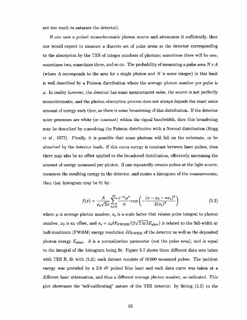
not too much to saturate the detector).
If one uses a pulsed monochromatic photon source and attenuates it sufficiently, then
one would expect to measure a discrete set of pulse areas at the detector corresponding
to the absorption by the TES of integer numbers of photons; sometimes there will be one,
sometimes two, sometimes three, and so on. The probability of measuring a pulse area N x A
(where A corresponds to the area for a single photon and N is some integer) in this limit
is well described by a Poisson distribution where the average photon number per pulse is
fi. In reality however, the detector has some measurement noise, the source is not perfectly
monochromatic, and the photon absorption process does not always deposit the exact same
amount of energy each time, so there is some broadening of this distribution. If the detector
noise processes are white (or constant) within the signal bandwidth, then this broadening
may be described by convolving the Poisson distribution with a Normal distribution (Hogg
et al., 1972). Finally, it is possible tha t some photons will fall on the substrate, or be
absorbed by the detector leads. If this extra energy is constant between laser pulses, then
there may also be an offset applied to the broadened distribution, effectively increasing the
amount of energy measured per photon. If one repeatedly creates pulses at the light source,
measures the resulting energy in the detector, and makes a histogram of the measurements,
then tha t histogram may be fit by:
f ( x ) - A V , j : n ( . . . ( * - i o - n * . ) 2 \ ( r 2 j
where ji is average photon number, xs is a scale factor tha t relates pulse integral to photon
number, xo is an offset, and as = o;s<5Efwhm/(2v/2 In 2 £ ’phot) is related to the full-width at
half-maximum (FWHM) energy resolution <5jEf w h m °f the detector as well as the deposited
photon energy Ephot- A is a normalization parameter (not the pulse area), and is equal
to the integral of the histogram being fit. Figure 5.7 shows three different data sets taken
with TES B, fit with (5.2); each dataset consists of 10000 measured pulses. The incident
energy was provided by a 2.6 eV pulsed blue laser and each data curve was taken at a
different laser attenuation, and thus a different average photon number, as indicated. This
plot showcases the “self-calibrating” nature of the TES detector: by fitting (5.2) to the
62
oo400o
® 800
c3
Uro
1000
200
600
0
O 3 2 % Intensity | i - 0.124
SEpWHM = ^
A 6 3 % in ten sity
□ 1 0 0 % in ten sity
■ g = 0.247 ^Efvvhm = 1 -33 eV
■ g = 0.40 6Efwhm = 1.49 eV■FWHM
■FWNM “ 1 •
0 1 2 3Average photon number
Figure 5.7: Histograms of pulse areas at three different attenuations measured with TES B. Reprinted with permission from Carter et al. (2014) (c) IEEE 2014. The light-source was a pulsed 2.6 eV laser. The histograms are all fit by (5.2).
histogram of measured pulse areas (or pulse heights, as height is proportional to area for
an exponential pulse) one may determine the pulse area (or height) tha t corresponds to the
absorption of a single photon of known energy. W ith this value in-hand, a light-source of
unknown energy may be applied to the TES, and its spectrum may be determined. This
only works in the limit tha t the unknown source is attenuated sufficiently tha t no more
than a single photon is ever incident on the TES at a time as simultaneous absorption of
two photons of different energy could confuse the issue.
TES B was by far the best functioning TES produced during this research, and the
only one tha t was directly amenable to this simple “self-calibration” routine. For reasons
discussed briefly in section 4.3.2, TES B was somehow dirty (as determined by its higher-
than-normal resistivity), and likely chemically distinct (due to the fabrication process) from
the other TESs measured in this work, which were all elemental Ti. Unfortunately, it met
an early demise due to an accident involving high-voltage. Analyzing and understanding
the pulse measurements from the other TESs required more care and analysis, and is the
subject of the next chapter.
63
TES calibrations uChapter
EFFICIENCY (rj) is one of the most important things to know about a TES tha t is single
photon sensitive. Although the TES pulse area is proportional to energy absorbed,
one must know what fraction of the photon’s energy is absorbed to accurately measure
the energy of an unknown incident photon. However, in order to measure 77, one must first
satisfy the requirement tha t the TES be single photon sensitive. The simplest way to do this
is to use a pulsed monochromatic source, attenuated to an average intensity of < 1 photon
incident on the detector per pulse, and fit the resulting pulse area histogram to (5.2). This
histogram can also be used to confirm the linearity of the energy response (but not the
efficiency) of the TES at higher energies, which is important because the blue photons have
lower energy than the intended vacuum UV signal emitted by the helium excimers. This
chapter is divided into three main parts. Section 6.1 discusses the first three TESs created
for this project and details their response to blue (and in some cases near-IR) photons. For
various reasons, each one of these TESs was found unsuitable for the ultim ate goal of the
project, which was the detection of helium excimers. However, the particular failings of
each TES informed the design of the TES tha t followed, and those points are discussed in
this section. Section 6.2 discusses the three TESs (D, E, and F) tha t were used to detect
excimers. The only difference between these three devices is tha t devices E and F had an
extra ~20 nm thick layer of sputtered metal; gold for TES E, and platinum for TES F.
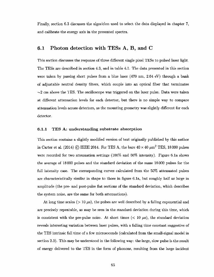
Finally, section 6.3 discusses the algorithm used to select the data displayed in chapter 7,
and calibrate the energy axis in the presented spectra.
6.1 Photon detection w ith TESs A, B, and C
This section discusses the response of three different single pixel TESs to pulsed laser light.
The TESs are described in section 4.3, and in table 4.1. The data presented in this section
were taken by passing short pulses from a blue laser (470 nm, 2.64 eV) through a bank
of adjustable neutral density filters, which couple into an optical fiber tha t terminates
~ 2 cm above the TES. The oscilloscope was triggered on the laser pulse. D ata were taken
at different attenuation levels for each detector, but there is no simple way to compare
attenuation levels across detectors, as the mounting geometry was slightly different for each
detector.
6.1 .1 T E S A: understan d ing su b stra te absorption
This section contains a slightly modified version of text originally published by this author
in Carter et al. (2014) © IEEE 2014. For TES A, the bare 40 x 40 / i in 2 TES, 18000 pulses
were recorded for two attenuation settings (100% and 50% intensity). Figure 6.1a shows
the average of 18 0 0 0 pulses and the standard deviation of the same 18 0 0 0 pulses for the
full intensity case. The corresponding curves calculated from the 50% attenuated pulses
are characteristically similar in shape to those in figure 6 .1 a, but roughly half as large in
amplitude (the pre- and post-pulse flat sections of the standard deviation, which describes
the system noise, are the same for both attenuations).
At long time scales (> 10 /us), the pulses are well described by a falling exponential and
are precisely repeatable, as may be seen in the standard deviation during this time, which
is consistent with the pre-pulse noise. At short times ( < 1 0 fis), the standard deviation
reveals interesting variation between laser pulses, with a falling time constant suggestive of
the TES intrinsic fall time of a few microseconds (calculated from the small-signal model in
section 2.3). This may be understood in the following way: the large, slow pulse is the result
of energy delivered to the TES in the form of phonons, resulting from the large incident
65
I fw o« a| 5 <8 3
*s oc £30) (QI 3° 3
V ) <r=
50
Data from 18,000 traces40
Average of pulses Standard Deviation of pulses-30
3010
0Ion-zero value due to noise
-1080 1200 40
Time from trigger (ps)
(a) © IEEE 2014
Single trace■— Fast pulse template Slow pulse template
Total fit - fast + slow
40
fcE3
20
UJ
50 100 150-50 0
Time from trigger (ps)
(b) © IEEE 2014
Q.Ooo
DoO
16001 J i t 1 1 1 1 1
ST H ----- 50% intensity/ ft ...... p - 0.122
1400 - 1 1 x0/xs * 0.59 photons"
1200f1
SEfWHM = 1.96 eV
1000 i 5f ^ ----- 100% intensity
800 - f ft \ ...... p - 0.255J M vL Xo/xs * 1 -26 photons
600 ■ r / 1 \ \ &Efwhm - 2 4 4 eV400 - / I V. \ li.2 0 0 - / J -V '^CA
A
0 100 200
Integral of fit to fast pulse (femto-Coulombs)
(c) © IEEE 2014
3.0
2.5>V2.0co*•>
8e □ Data from blue laser Fit to blue laser
gs 1.0 gm 0 .5
□ Data from IR laser — Fit to IR laser
o.o60 2 3 51 4
Average photon number
(d)
Raw data, single trace Fit to fast pulse Fit to slow pulse Total f i t » fast + slow
20
5 -
-20 0 20 40 60x10'Time from trigger (s)
(e)
.... i ...n.....------No attenuation........Fit n - 5.98
a « 1.45X o -6 .5 fC
\ r \ ----- Attenuation 50% -\ J J U ........Fit p - 3.04Jfll l l \ o - l . 1 7
is* / n M Xo < 0.1 fC
i f Ji *1 vij ----- Attenuation 67% _I V Vi ........Fit n - 1.89\ \» \ o - 1.05\ \ \ xo < 0 .1 fC
0 20 40 60 80
Integral of fit to fast pulse (femto-Coulombs)
(f)
Figure 6.1: The first three panels summarize the response of TES A to blue laser light and are reprinted with permission from Carter et al. (2014). The fourth panel compares the energy resolution of TES A (at two different wavelengths of light) as a function of laser intensity. The final two panels summarize the response of TES A to IR laser light. See the text for more detailed descriptions.
66
photon flux on the substrate outside the area of the TES. The faster, smaller component
(the component which varies from pulse to pulse) arises from direct photon hits to the TES.
These small, fast pulses are the more interesting component of the data, as they should obey
Poisson statistics and can also be directly modeled by the equations in section 2.3.
The standard deviation can be used as a model pulse template for the fast component
if one assumes three sources of fluctuations in the TES pulses: fluctuations due to noise
processes tha t are not related to the photon pulses <tn, fluctuations due to a varying amount
of power absorbed by the substrate crsi, and fluctuations due to the varying number of
photons directly absorbed in the detector <t t e s - If one assumes these three sources of
fluctuations are uncorrelated then they add in quadrature and the to tal RMS fluctuations
(plotted in figure 6 .1 a, black curve) are described by a2 = + crgj + a ^ ES; this equation
is easily rearranged to give <t t e s a s a function of the other variables. Since the standard
deviation of a set of exponential pulses with different amplitudes, but identical rise and fall
times, is an exponential pulse of the same character, cttes is therefore an excellent template
for the fast pulse tha t contains the information about direct photon hits to the TES. Prom
figure 6 .1 a it is clear tha t <rsi < ctn (since there is no apparent variation on the 2 0 ps
timescale) and tha t <tn is constant over time, and so the model for a good pulse template
(<7t e s ) is easily computed.
One may then use a double exponential (one rising, one falling) pulse shape to fit the
rise and fall of c t t e s and then use this fit function a s a template to extract the fast pulse
component from each individual trace. Because all the fast pulses have the same character,
only the amplitude should vary; the decay time, rise time, and starting time of the template
should be fixed between pulses. This fast-pulse model may then be used, along with the
average of the data, to infer a model for the slow pulse (also a double exponential). Finally,
as with the fast pulse template, the slow pulse template parameters must be fixed, save
for the amplitude, and the full model (now with only the two model pulse amplitudes as
free parameters) may be fit to all 18000 traces. One of these fits is depicted in figure 6.1b.
The fast pulse fits were then integrated and histograms were made for both attenuations
(figure 6 .1 c).
The histograms were fit to the first 20 terms of (5.2). The initial guess for xs was
67
calculated by plugging all the measured device parameters into the small-signal model,
generating a model pulse for a single photon, and integrating the model. Likewise, the
initial guess for as was calculated from the small-signal model. The scale factor A is a fixed
parameter and is equal to the area of the histogram being fit.
One may calculate < 5 £ 7 fw h m from as. For the full intensity histogram, a = <ts/ x s = 0.39
and (5-Efwhm = 2.44 eV. It is interesting to compare this to the intrinsic device resolution
calculated from the small-signal model, ^ fw h m = 0.6 eV. The full system resolution is
roughly four times worse than the theoretical value from the model, but tha t is reason
able given tha t over much of the bandwidth amplifier and electronic noise dominate (see
figure 5.6), rather than intrinsic TES noise.
The fact tha t xq and a component of 5-EpwHM 9X6 both linearly proportional to fi
implies tha t there is some extra signal tha t is unaccounted for in the two-pulse model. If
the contribution from the constant external input from substrate events (the slow pulse) is
imperfectly modeled, then there will be a residual amount of energy in every fast pulse. This
residual energy will be constant across measured pulses, independent of how many photons
directly hit the TES, and will manifest as a constant offset from zero for the histogram that
scales with laser intensity. TES A ’s energy resolution in the absence of a substrate signal
may be estimated by fitting a straight line to a plot of <5Ef w h m vs- AL and extracting the
y-intercept. This calculation gives <5£ f w h m — 1-52 eV, and is depicted in figure 6. Id.
One way to test the assumption tha t the slow pulse is due to photon absorption in the
substrate is to repeat the experiment with an infrared laser with a wavelength of 1550 nm
(~0.8 eV). At this wavelength, the Si substrate is nearly transparent, and so the absorption
should be much less. Figure 6.1e depicts an example of the model fit to an IR photon
detection event. Note the relative heights of the slow and fast contributions is inverted from
the blue laser case. Figure 6.If shows histograms from three different attenuations of the IR
laser. The <5Efwhm is plotted against average photon number for the IR data in figure 6.Id.
The slope of this line is more shallow than the corresponding line for the blue laser data,
indicating tha t a smaller fraction of the energy resolution is due to substrate events. The
fact tha t both curves intersect at n = 0 is not surprising, as tha t point represents the
best-case energy resolution in the absence of any broadening due to substrate absorption.
68
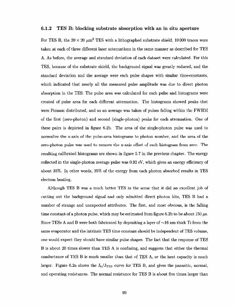
6.1 .2 T E S B: b locking su b stra te absorption w ith an in s itu aperture
For TES B, the 20 x 20 fim2 TES with a lithographed substrate shield, 10000 traces were
taken at each of three different laser attenuations in the same manner as described for TES
A. As before, the average and standard deviation of each dataset were calculated. For this
TES, because of the substrate shield, the background signal was greatly reduced, and the
standard deviation and the average were each pulse shapes with similar time-constants,
which indicated tha t nearly all the measured pulse amplitude was due to direct photon
absorption in the TES. The pulse area was calculated for each pulse and histograms were
created of pulse area for each different attenuation. The histograms showed peaks that
were Poisson distributed, and so an average was taken of pulses falling within the FWHM
of the first (zero-photon) and second (single-photon) peaks for each attenuation. One of
these pairs is depicted in figure 6.2b. The area of the single-photon pulse was used to
normalize the x-axis of the pulse-area histograms to photon number, and the area of the
zero-photon pulse was used to remove the x-axis offset of each histogram from zero. The
resulting calibrated histograms are shown in figure 5.7 in the previous chapter. The energy
collected in the single-photon average pulse was 0.92 eV, which gives an energy efficiency of
about 35%. In other words, 35% of the energy from each photon absorbed results in TES
electron heating.
Although TES B was a much better TES in the sense tha t it did an excellent job of
cutting out the background signal and only admitted direct photon hits, TES B had a
number of strange and unexpected attributes. The first, and most obvious, is the falling
time constant of a photon pulse, which may be estimated from figure 6.2b to be about 150 /is.
Since TESs A and B were both fabricated by depositing a layer of ~16 nm thick Ti from the
same evaporator and the intrinsic TES time constant should be independent of TES volume,
one would expect they should have similar pulse shapes. The fact tha t the response of TES
B is about 20 times slower than TES A is confusing, and suggests tha t either the thermal
conductance of TES B is much smaller than tha t of TES A, or the heat capacity is much
larger. Figure 6.2a shows the Ib/IrES curve for TES B, and gives the parasitic, normal,
and operating resistances. The normal resistance for TES B is about five times larger than
69
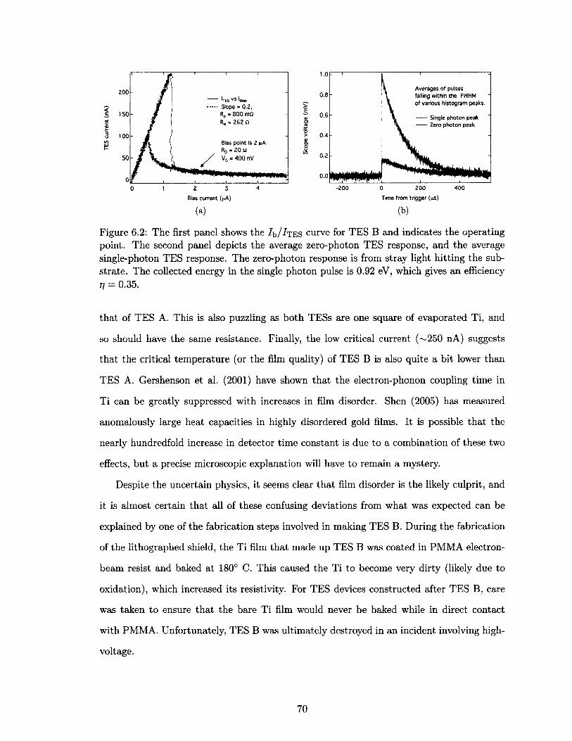
Averages of pulses falling within the FWHM of various histogram peaks.
0.8
0.6 Single photon peak Zero photon peak
0.0
200 400-200 0
200hxs vs taas Slope * 0.2, Rp * 800 mQ Rn - 262 Q
1 150cpfc3 100V) Bias point is 2 pA
R o « 2 0 Q V0 * 400 nV
0 2 3 41
Bias current (pA) Time from trigger (ps)
(a) (b)
Figure 6.2: The first panel shows the /b/^TES curve for TES B and indicates the operating point. The second panel depicts the average zero-photon TES response, and the average single-photon TES response. The zero-photon response is from stray light hitting the substrate. The collected energy in the single photon pulse is 0.92 eV, which gives an efficiency 77 = 0.35.
tha t of TES A. This is also puzzling as both TESs are one square of evaporated Ti, and
so should have the same resistance. Finally, the low critical current (~250 nA) suggests
tha t the critical tem perature (or the film quality) of TES B is also quite a bit lower than
TES A. Gershenson et al. (2001) have shown tha t the electron-phonon coupling time in
Ti can be greatly suppressed with increases in film disorder. Shen (2005) has measured
anomalously large heat capacities in highly disordered gold films. It is possible tha t the
nearly hundredfold increase in detector time constant is due to a combination of these two
effects, but a precise microscopic explanation will have to remain a mystery.
Despite the uncertain physics, it seems clear tha t film disorder is the likely culprit, and
it is almost certain tha t all of these confusing deviations from what was expected can be
explained by one of the fabrication steps involved in making TES B. During the fabrication
of the lithographed shield, the Ti film tha t made up TES B was coated in PMMA electron-
beam resist and baked at 180° C. This caused the Ti to become very dirty (likely due to
oxidation), which increased its resistivity. For TES devices constructed after TES B, care
was taken to ensure tha t the bare Ti film would never be baked while in direct contact
with PMMA. Unfortunately, TES B was ultimately destroyed in an incident involving high-
voltage.
70
Q)U2
1 us pulse areas normalized to photon number.
(Q§ 0.8
Fit: n » 0.19 photons o ffse t - 0 .17 photons O -0 .1 7§o
■gNre0.2
z
0.00 2 3 4
50
A v e r a g e s o f p u l s e s fa ll in g w i th in t h e FW HM o f v a r io u s h i s t o g r a m p e a k s .
40
30 Single photon peak Zero photon peak
20
10
00 2 6 8 10 124
Photon num ber Time from trigger (ps)
(a) (b)
Figure 6.3: The left panel shows a histogram of pulse areas normalized to photon number from TES C. The right panel shows zero-photon and one-photon average pulse shapes made by averaging together traces tha t fell within the zero- and one-photon peaks of the histogram in the left panel.
6 .1 .3 T E S C: b lock ing su b stra te absorption w ith a su b stra te m irror
TES C was designed to block the substrate from photon absorption and to avoid the com
plicated (and possibly damaging) fabrication steps required to create a lithographed shield.
Instead of creating an aperture over TES C, the entire substrate was coated with aluminum,
save for under the TES, and for a thin border around the TES, which electrically isolated
it from the rest of the substrate. This aluminum coating was intended to act as a mirror,
reflecting any incident light away from the substrate. Although not as successful as the
lithographed shield used on TES B at shielding the substrate from incident light, the re
flective coating reduces the background contribution to a point where it is well below the
signal from the blue photons. Figure 6.3b shows the average signal recorded when zero
photons were incident on the TES (dark blue), and also when a single photon was incident
on the TES (light blue). The substrate signal is non-zero because the mirror-coating is not
complete. There is an exposed area surrounding the TES pixel where light may be absorbed
by the substrate.
In order to get the best possible estimate of the pulse area due to the direct photon
hits, pulse areas were only recorded between 0 /is and 1 fis from the trigger. In this region,
the direct TES hit signal to substrate signal is maximized. The histogram in figure 6.3a
71
was created by binning these 1 [is pulse areas, fitting the histogram to (5.2), and then
normalizing the areas to photon number so tha t x s = 1. Overall, the fit to (5.2) is good,
however there is a region between the zero- and one- photon peaks, and also a region between
the one- and two- photon peaks, where there are more counts than would be expected for
Poisson distributed data. Identifying the cause of this excess signal is largely the subject of
the next section.
6.2 Photon detection w ith TESs D, E, and F
TESs D, E, and F were made smaller than TES C to increase the amount of heating
(and therefore the pulse height for a given energy input) and were constructed with built-
in shields. The shield design was the same as tha t used for TES B, however a different
fabrication process was used to ensure tha t the Ti TES surface was not contaminated by
interaction with the electron-beam resist. TESs E and F were identical to TES D, but
also had an additional thin layer ( ~ 2 0 nm) of sputtered metal added as a final step to the
fabrication process. TES E was coated with gold, and TES F was coated with platinum.
These two metals were chosen as they are both very resistant to corrosion, and have a high
work function, both which are im portant when detecting triplet state excimers directly (see
chapter 7). TES E will not be discussed in this section as the device was qualitatively
similar to TES F (thin metal layer on top of a TES).
6.2 .1 T E S D: searching for th e source o f an ex tra unw anted signal
As discussed in the previous sections, a large amount of effort has gone in to designing a
detector tha t allows photons to couple into the detector, but not into the substrate. From
figures 6.2b and 6.3b, it is evident tha t neither a substrate shield nor a reflective substrate
coating is entirely sufficient to keep energy out of the substrate; even when no photon is
absorbed directly in the TES, some energy always couples in through the substrate. This
substrate response is proportional to laser intensity as shown in figure 6 .Id. In the analysis
of TES C’s photon response, it was noted tha t there was a population of pulses tha t were
not well-described by a Poisson distribution. This population is also present in the results
72
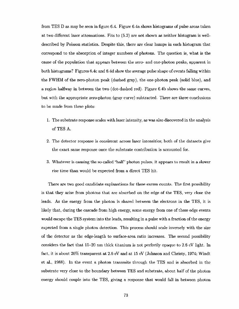
from TES D as may be seen in figure 6.4. Figure 6.4a shows histograms of pulse areas taken
at two different laser attenuations. Fits to (5.2) are not shown as neither histogram is well-
described by Poisson statistics. Despite this, there are clear humps in each histogram that
correspond to the absorption of integer numbers of photons. The question is, what is the
cause of the population tha t appears between the zero- and one-photon peaks, apparent in
both histograms? Figures 6.4c and 6.4d show the average pulse shape of events falling within
the FWHM of the zero-photon peak (dashed gray), the one-photon peak (solid blue), and
a region halfway in between the two (dot-dashed red). Figure 6.4b shows the same curves,
but with the appropriate zero-photon (gray curve) subtracted. There are three conclusions
to be made from these plots:
1. The substrate response scales with laser intensity, as was also discovered in the analysis
of TES A.
2. The detector response is consistent across laser intensities; both of the datasets give
the exact same response once the substrate contribution is accounted for.
3. W hatever is causing the so-called “h a lf’ photon pulses, it appears to result in a slower
rise time than would be expected from a direct TES hit.
There are two good candidate explanations for these excess counts. The first possibility
is that they arise from photons tha t are absorbed on the edge of the TES, very close the
leads. As the energy from the photon is shared between the electrons in the TES, it is
likely that, during the cascade from high energy, some energy from one of these edge events
would escape the TES system into the leads, resulting in a pulse with a fraction of the energy
expected from a single photon detection. This process should scale inversely with the size
of the detector as the edge-length to surface-area ratio increases. The second possibility
considers the fact tha t 15-20 nm thick titanium is not perfectly opaque to 2.6 eV light. In
fact, it is about 20% transparent at 2.6 eV and at 15 eV (Johnson and Christy, 1974; W indt
et al., 1988). In the event a photon transm its through the TES and is absorbed in the
substrate very close to the boundary between TES and substrate, about half of the photon
energy should couple into the TES, giving a response tha t would fall in between photon
73
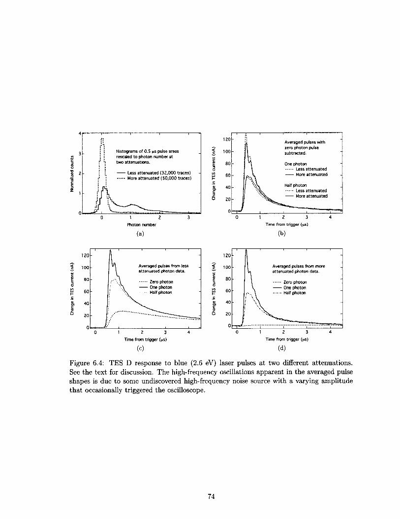
----- --T ....... ....................T...... ................ 1 1 "
1 2 0
i ■............. i ....................... i i i
; Averaged pulses with
Histograms of 0.5 \xs puise areas rescaled to photon number at
i zero photon pulse- c 1 0 0 1 subtracted.
• two attenuations. S□80 - ^ One photon
\ ...... Less attenuated-
- ;f -------Less attenuated (32,000 traces) 10 60 . ti -------More attenuated: — More attenuated (50,000 traces) H
V 40 / Half photonj r c 'vV ........ Less attenuated
h X2 0
----- More attenuated; l. u - -
i* r— r i 0 1 1 1 ----- ------i—
1 2
Photon number
(a)
1 2 3Time from trigger (j*s)
(b)
120
Averaged pulses from less attenuated photon data.
0 0
60 — Zero photon— One photon
Half photon60
40o>
20
0 1 2 3 4Time from trigger (ps)
(c)
120
Averaged pulses from more attenuated photon data.
100
Zero photon One photon Half photon60
40
2 3 40 1
Time from trigger (ps)
(d)
Figure 6.4: TES D response to blue (2.6 eV) laser pulses at two different attenuations. See the text for discussion. The high-frequency oscillations apparent in the averaged pulse shapes is due to some undiscovered high-frequency noise source with a varying amplitude tha t occasionally triggered the oscilloscope.
74
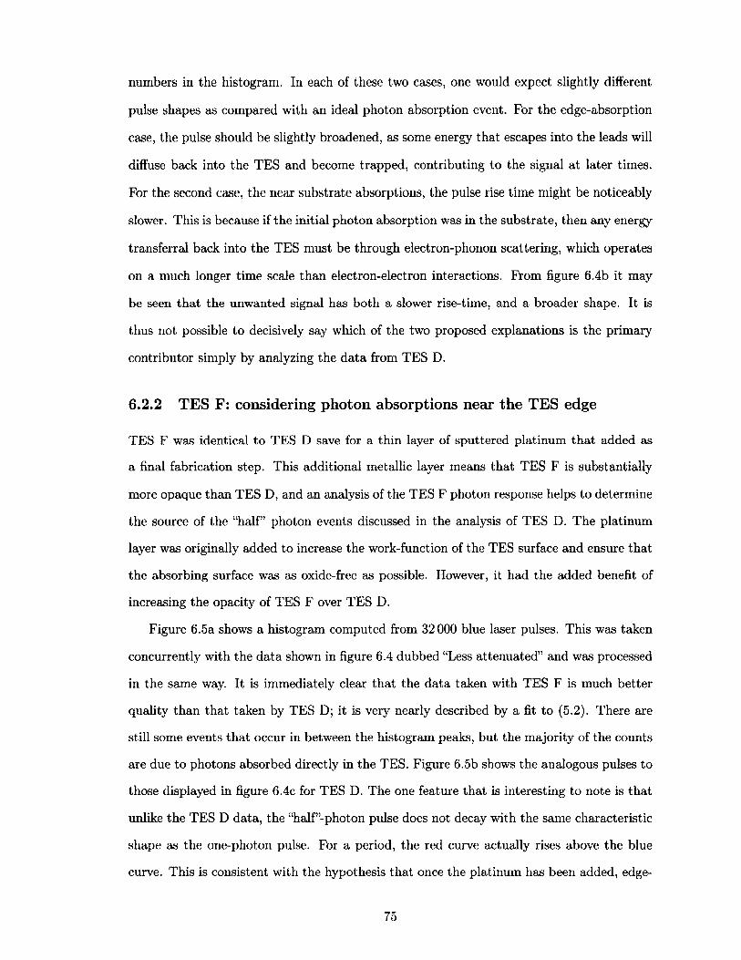
numbers in the histogram. In each of these two cases, one would expect slightly different
pulse shapes as compared with an ideal photon absorption event. For the edge-absorption
case, the pulse should be slightly broadened, as some energy tha t escapes into the leads will
diffuse back into the TES and become trapped, contributing to the signal at later times.
For the second case, the near substrate absorptions, the pulse rise time might be noticeably
slower. This is because if the initial photon absorption was in the substrate, then any energy
transferral back into the TES must be through electron-phonon scattering, which operates
on a much longer time scale than electron-electron interactions. From figure 6.4b it may
be seen tha t the unwanted signal has both a slower rise-time, and a broader shape. It is
thus not possible to decisively say which of the two proposed explanations is the primary
contributor simply by analyzing the data from TES D.
6.2 .2 T E S F: considering p h oton absorption s near th e T ES edge
TES F was identical to TES D save for a thin layer of sputtered platinum tha t added as
a final fabrication step. This additional metallic layer means tha t TES F is substantially
more opaque than TES D, and an analysis of the TES F photon response helps to determine
the source of the “h a lf’ photon events discussed in the analysis of TES D. The platinum
layer was originally added to increase the work-function of the TES surface and ensure that
the absorbing surface was as oxide-free as possible. However, it had the added benefit of
increasing the opacity of TES F over TES D.
Figure 6.5a shows a histogram computed from 32 000 blue laser pulses. This was taken
concurrently with the data shown in figure 6.4 dubbed “Less attenuated” and was processed
in the same way. It is immediately clear that the data taken with TES F is much better
quality than tha t taken by TES D; it is very nearly described by a fit to (5.2). There are
still some events tha t occur in between the histogram peaks, but the majority of the counts
are due to photons absorbed directly in the TES. Figure 6.5b shows the analogous pulses to
those displayed in figure 6.4c for TES D. The one feature tha t is interesting to note is that
unlike the TES D data, the “h a lf’-photon pulse does not decay with the same characteristic
shape as the one-photon pulse. For a period, the red curve actually rises above the blue
curve. This is consistent with the hypothesis tha t once the platinum has been added, edge-
75
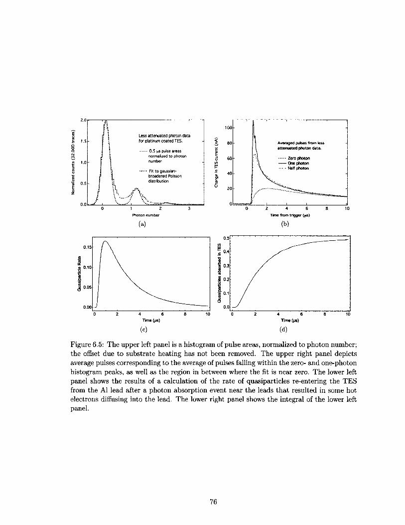
2.0
M4>O Less attenuated photon data for platinum coated TES.
oooOJto0.5 ps pulse areas normalized to photon numberV>£3Oo Fit to gaussian- broadened Poisson distributionN
0.5§oz
0.00 2 3
Photon number
(a)
100
<c Averaged pulses a ttenuated photon data.
80 less
3Uonpc
•— Zero photon— One photon— Half photon
«>O)CMJZu 20
0 2 4 6 8 10
Time from trigger (ps)
(b)
0.15
o 0.10
8 0.05
0.000 2 4 6 8 10
Time (ps)
0.5
0.4
0.3
0.2
« 0.1
0.00 2 4 6 8 10
Time (ps)
Figure 6.5: The upper left panel is a histogram of pulse areas, normalized to photon number; the offset due to substrate heating has not been removed. The upper right panel depicts average pulses corresponding to the average of pulses falling within the zero- and one-photon histogram peaks, as well as the region in between where the fit is near zero. The lower left panel shows the results of a calculation of the rate of quasiparticles re-entering the TES from the A1 lead after a photon absorption event near the leads tha t resulted in some hot electrons diffusing into the lead. The lower right panel shows the integral of the lower left panel.
76

hits are the primary cause of the events that deviate from a Poisson distribution. If a photon
is absorbed close enough to the leads, some energy from the photon will be converted into
quasiparticles in the aluminum. These quasiparticles will diffuse along the aluminum, and
some of them will reenter the TES. The quasiparticles tha t return to the TES will do so
on a time-scale tha t depends on the diffusion constant and the quasiparticle lifetime in Al.
Figure 6.5c shows the fractional quasiparticle arrival rate into the TES from the leads as a
function of time, modeled in M athematica (see appendix C for the code, and appendix A
for a discussion of the diffusion model), for the case where a population of quasiparticles
is created on the boundary of the TES and a long aluminum lead. Figure 6.5d gives the
fraction of initial quasiparticle population injected into the TES over time. Values for the
diffusion constant and quasiparticle lifetime of Al were taken from Wang et al. (2014), a
work tha t measured the properties of aluminum evaporated from the same machine used
to create the detectors for this experiment. The electron-electron scattering time in the Ti
was set at 10 ns for the simulation. The time-scale of quasiparticles entering the TES from
the leads, as calculated by this model, is consistent with the small increase in TES response
seen at late times in the “half-photon pulse.
Now tha t the unwanted signal has been tentatively identified as arising from photon
hits in the TES tha t are close to the leads (at least for TESs E and F), it is interesting
to estimate what fraction of the TES area gives “good” responses (all the available photon
energy couples into the TES). The integral of the fit-curve in figure 6.5a is 0.85. Since
the data histogram was normalized to an area of 1, this means tha t 15% of the data falls
outside the fit, and may be attributed to edge-hits. The integral of the zero-photon Gaussian
peak in the fit curve is 0.68, which means that for 6 8 % of events, the TES had no photon
incident upon it. The remaining 17% of events, then are “good” data in the sense tha t they
correspond to the data tha t is described by the fit. If photon flux is uniformly incident on
the TES, this analysis suggests tha t 47% of the photons absorbed in the TES are edge-hits.
Since edge hits are adjacent to an edge, and TES F is 15 fim long and symmetric in the
width dimension, then it may be inferred tha t a photon absorption within 3.5 fim of either
lead may be classified as an unwanted edge-hit.
Finally, whether it is possible to easily remove the unwanted signals, regardless of origin,
77
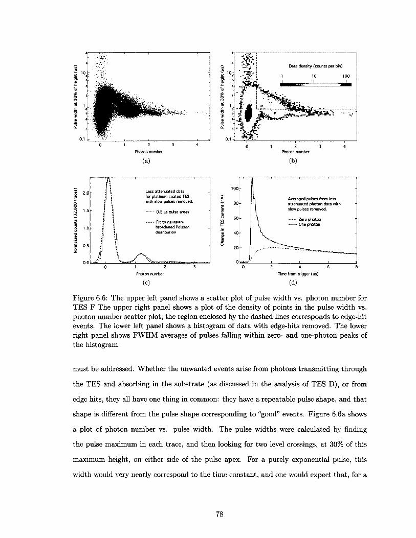
2.0
1.0
0.5
0.0
1 2 3
Photon number
(a)
Less attenuated data for platinum coated TES with slow pulses removed.
0.5 (xs pulse areas
Fit to gaussian- broadened Poisson distribution
1 2
Photon number
(c)
Data density (counts per bin)V)a.r io- £ 8- .2> 6. Vf 4.Oo 2ro
100
£%I8£
0 1 2Photon number
3 4
(b)
100
Averaged pulses from less attenuated photon data with slow pulses removed.
3O</)c
€0 Zero photon One photon
40v?n£o
20
0 2 6 84
Time from trigger (ps)
(d)
Figure 6 .6 : The upper left panel shows a scatter plot of pulse width vs. photon number for TES F The upper right panel shows a plot of the density of points in the pulse width vs. photon number scatter plot; the region enclosed by the dashed lines corresponds to edge-hit events. The lower left panel shows a histogram of data with edge-hits removed. The lower right panel shows FWHM averages of pulses falling within zero- and one-photon peaks of the histogram.
must be addressed. W hether the unwanted events arise from photons transm itting through
the TES and absorbing in the substrate (as discussed in the analysis of TES D), or from
edge hits, they all have one thing in common: they have a repeatable pulse shape, and that
shape is different from the pulse shape corresponding to “good” events. Figure 6 .6 a shows
a plot of photon number vs. pulse width. The pulse widths were calculated by finding
the pulse maximum in each trace, and then looking for two level crossings, at 30% of this
maximum height, on either side of the pulse apex. For a purely exponential pulse, this
width would very nearly correspond to the time constant, and one would expect that, for a
78
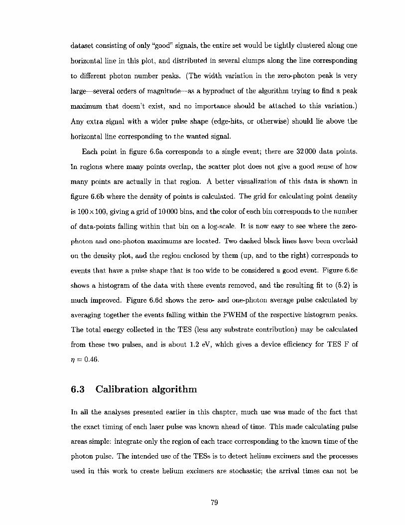
dataset consisting of only “good” signals, the entire set would be tightly clustered along one
horizontal line in this plot, and distributed in several clumps along the line corresponding
to different photon number peaks. (The width variation in the zero-photon peak is very
large—several orders of magnitude—as a byproduct of the algorithm trying to find a peak
maximum tha t doesn’t exist, and no importance should be attached to this variation.)
Any extra signal with a wider pulse shape (edge-hits, or otherwise) should lie above the
horizontal line corresponding to the wanted signal.
Each point in figure 6 .6 a corresponds to a single event; there are 32000 data points.
In regions where many points overlap, the scatter plot does not give a good sense of how
many points are actually in tha t region. A better visualization of this data is shown in
figure 6 .6 b where the density of points is calculated. The grid for calculating point density
is 1 0 0 x 1 0 0 , giving a grid of 1 0 0 0 0 bins, and the color of each bin corresponds to the number
of data-points falling within tha t bin on a log-scale. It is now easy to see where the zero-
photon and one-photon maximums are located. Two dashed black lines have been overlaid
on the density plot, and the region enclosed by them (up, and to the right) corresponds to
events th a t have a pulse shape tha t is too wide to be considered a good event. Figure 6 .6 c
shows a histogram of the data with these events removed, and the resulting fit to (5.2) is
much improved. Figure 6 .6 d shows the zero- and one-photon average pulse calculated by
averaging together the events falling within the FWHM of the respective histogram peaks.
The total energy collected in the TES (less any substrate contribution) may be calculated
from these two pulses, and is about 1.2 eV, which gives a device efficiency for TES F of
rj = 0.46.
6.3 Calibration algorithm
In all the analyses presented earlier in this chapter, much use was made of the fact tha t
the exact timing of each laser pulse was known ahead of time. This made calculating pulse
areas simple: integrate only the region of each trace corresponding to the known time of the
photon pulse. The intended use of the TESs is to detect helium excimers and the processes
used in this work to create helium excimers are stochastic; the arrival times can not be
79
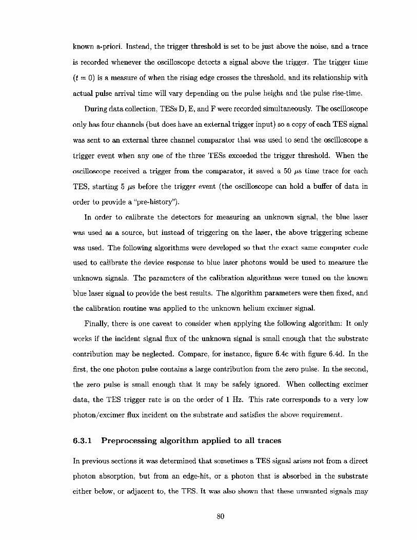
known a-priori. Instead, the trigger threshold is set to be just above the noise, and a trace
is recorded whenever the oscilloscope detects a signal above the trigger. The trigger time
(t = 0 ) is a measure of when the rising edge crosses the threshold, and its relationship with
actual pulse arrival time will vary depending on the pulse height and the pulse rise-time.
During data collection, TESs D, E, and F were recorded simultaneously. The oscilloscope
only has four channels (but does have an external trigger input) so a copy of each TES signal
was sent to an external three channel comparator tha t was used to send the oscilloscope a
trigger event when any one of the three TESs exceeded the trigger threshold. W hen the
oscilloscope received a trigger from the comparator, it saved a 50 fj,s time trace for each
TES, starting 5 /is before the trigger event (the oscilloscope can hold a buffer of data in
order to provide a “pre-history”).
In order to calibrate the detectors for measuring an unknown signal, the blue laser
was used as a source, but instead of triggering on the laser, the above triggering scheme
was used. The following algorithms were developed so tha t the exact same computer code
used to calibrate the device response to blue laser photons would be used to measure the
unknown signals. The parameters of the calibration algorithms were tuned on the known
blue laser signal to provide the best results. The algorithm parameters were then fixed, and
the calibration routine was applied to the unknown helium excimer signal.
Finally, there is one caveat to consider when applying the following algorithm: It only
works if the incident signal flux of the unknown signal is small enough tha t the substrate
contribution may be neglected. Compare, for instance, figure 6.4c with figure 6.4d. In the
first, the one photon pulse contains a large contribution from the zero pulse. In the second,
the zero pulse is small enough tha t it may be safely ignored. When collecting excimer
data, the TES trigger rate is on the order of 1 Hz. This rate corresponds to a very low
photon/excimer flux incident on the substrate and satisfies the above requirement.
6 .3 .1 P reprocessin g algorithm applied to all traces
In previous sections it was determined tha t sometimes a TES signal arises not from a direct
photon absorption, but from an edge-hit, or a photon tha t is absorbed in the substrate
either below, or adjacent to, the TES. It was also shown tha t these unwanted signals may
80
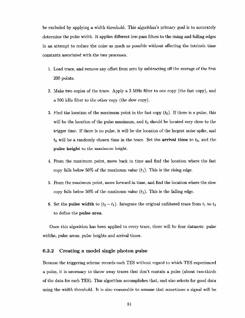
be excluded by applying a width threshold. This algorithm’s primary goal is to accurately
determine the pulse width. It applies different low-pass filters to the rising and falling edges
in an attem pt to reduce the noise as much as possible without affecting the intrinsic time
constants associated with the two processes.
1. Load trace, and remove any offset from zero by subtracting off the average of the first
2 0 0 points.
2. Make two copies of the trace. Apply a 3 MHz filter to one copy (the fast copy), and
a 500 kHz filter to the other copy (the slow copy).
3. Find the location of the maximum point in the fast copy (to)- If there is a pulse, this
will be the location of the pulse maximum, and to should be located very close to the
trigger time. If there is no pulse, it will be the location of the largest noise spike, and
to will be a randomly chosen time in the trace. Set the arrival tim e to to, and the
p u lse h e ig h t to the maximum height.
4. From the maximum point, move back in time and find the location where the fast
copy falls below 50% of the maximum value (t \ ). This is the rising edge.
5. From the maximum point, move forward in time, and find the location where the slow
copy falls below 50% of the maximum value (<2 )- This is the falling edge.
6 . Set the pulse width to ( £ 2 — h) . Integrate the original unfiltered trace from t\ to 12
to define the pulse area.
Once this algorithm has been applied to every trace, there will be four datasets: pulse
widths, pulse areas, pulse heights and arrival times.
6.3.2 Creating a model single photon pulse
Because the triggering scheme records each TES without regard to which TES experienced
a pulse, it is necessary to throw away traces tha t don’t contain a pulse (about two-thirds
of the data for each TES). This algorithm accomplishes that, and also selects for good data
using the width threshold. It is also reasonable to assume tha t sometimes a signal will be
81
due to an external event like an electrical fluctuation. These events should be present in all
three TESs, and tha t characteristic may be used to eliminate them.
1. For each set of simultaneous traces, calculate the fraction of total pulse area across
all three TESs according to: (TES pulse area)/(Sum of all three TES pulse areas).
Select data where this fraction is greater than 0.7.
2. From the data tha t survives the previous step, make a histogram of arrival times.
There should be a large peak near t = 0 corresponding to events tha t caused a trigger.
Select data that falls within this peak.
3. From the data tha t survives the previous step, make a density plot of pulse widths
vs. pulse areas, and use this plot to select a width threshold (rmax), keeping only the
data below the threshold. This step can, in principle, be automated, but is easy to
do manually and only needs to be done once.
4. Make a histogram of pulse areas from the data tha t survives the previous step. Average
together the original unfiltered pulses in the FWHM of the single-photon peak, which
should be clearly defined. This average is a good estimate of an ideal single photon
response.
5. Fit the single-photon average pulse to an analytical function. In the case of this
work, the best fit model was a pulse shape defined by one rising exponential and two
falling exponentials. The resulting model is the best possible estimate of the detector
response to a single photon.
The resulting model pulse may now be used as a calibration pulse. Any data processing
algorithm tha t calculates an area may be also applied to the model pulse to return the
“single-photon” area. The efficiency rj may be calculated by dividing the model pulse area
by the known photon energy (2.6 eV for the calibration laser used here).
6 .3 .3 U sin g th e pu lse m od el and th e noise traces to build a b e tter filter
Figure 7.1b shows a scatter plot of pulse heights vs. pulse areas for some helium excimer
data, which were conditioned according to the preprocessing algorithm 6.3.1. There are
82
three clear clusterings of data: two of traces tha t contain signal, and one of traces that
only contain noise. It is possible to use the noise traces, in conjunction with a model of the
desired signal, to create a filter tha t maximizes signal-to-noise. The method is described in
detail by Press et al. (2007), and the algorithm used in this work is given here.
1. Select only the noisy traces. Take a numerical Fourier Transform (FFT) of each trace,
and then calculate the magnitude squared of the FFTd trace. This is the unsealed
power spectrum (PS) of the noise in A2. Average all the noise PSs calculated this way
to get the total best estimate for the noise power spectrum 5 n -
2. Compute the model pulse’s power spectrum 5 m by taking the magnitude squared of
the FFT of the pulse model.
3. A filter ( / ) is then created according to / = 5m/(5m + 5^). This filter is a filter in
frequency space. It is near unity for frequencies where 5 m 2> 5 n , and close to zero
for frequencies where 5m •C 5n-
4. Apply the filter by taking the FFT of each trace, multiplying it by the filter, and then
inverting the FFT. This could also be accomplished by converting the filter to the
time domain and convolving it with each trace.
5. Filter the model pulse also, so tha t the effects of the filter on the pulse area may be
worked out.
Once the entire dataset of traces has been filtered in this way, the preprocessing algo
rithm is then run again to determine better estimates for pulse width, height, area, and
arrival time. Finally, the preprocessing algorithm is run on the filtered model pulse to get
the pulse area tha t corresponds to a single photon. The efficiency T) is the filtered model
pulse area divided by the photon energy.
6.3 .4 P rocessin g a lgorithm for exp erim en ta l d ata
1. Apply the algorithms described above to filter each pulse and then compute pulse
area and pulse width from the filtered data. For the filter creation, a new 5 n must be
83

calculated for each dataset as the noise contributions from each run might be different,
but S u comes from the intrinsic detector response and only needs to be calculated
once.
2. Apply the first two steps of the algorithm from section 6.3.2 and then reject any
remaining traces tha t have pulse widths greater than Tm a x .
3. Multiply the pulse areas by the bias-voltage. The resulting number is the uncalibrated
energy incident on the TES detector.
Once this algorithm has been applied to the unknown data, a histogram of incident
energies may be made. The energy axis is then scaled by dividing by r/ (which must be
calculated separately for each dataset as it depends on the filter used) and this corresponds
to the spectrum of energy incident on the TES. This process is how all the spectra in
chapter 7 were created.
84
Helium excimer /detections /
Chapter
T HERE were two methods used in this experiment to create helium excimers. The first
was to place a 22Na gamma-ray source outside the cryostat at the same height as the
superfluid chamber. Some fraction of the emitted gamma-rays pass through to the superfluid
bath and Compton scatter off an electron, causing a chain reaction of events tha t ends in
a cloud of both singlet and triplet excimers (Ito and Seidel, 2013). The second method is
to immerse a sharp tungsten tip in the superfluid bath and hold it at a voltage above the
electron emission threshold of the tip (~-1500 V in this experiment, although Guo et al.
(2009) report lower voltages). The ejected electrons lose their energy by scattering in the
superfluid bath, and the result is a cloud of excimers created near the tip. The first section
of this chapter discusses the detection of excimers created via gamma-ray excitation, and
the second discusses the detection of excimers created via electrons emitted from a sharp tip.
All the spectra shown in this chapter were produced according to the algorithms described
above in section 6.3.
One of the primary goals of this work was to detect (and differentiate between) both
the triplet state excimers and the singlet state excimers. The signal arising from singlet
decays should be straightforward to understand, as it ought to correspond directly to the
allowable spectrum of UV light produced during relaxation. The mechanism by which the
triplet state confers its energy to the TES is more nuanced, and is the subject of the final
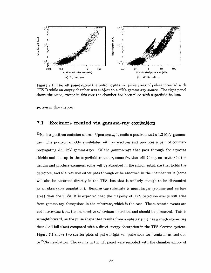
<c
0.01 0.1 10 1 0 0
Uncalibrated pulse area (eV)
(a) No helium
10
t 410
6 -4-
1 0 - "•
I—I M n ----- 1— I—i I 1111|------1—i ) 11 ni[-----1—i ! I ij
0.01 0.1 1 10 100 Uncalibrated pulse area (eV)
(b) With helium
Figure 7.1: The left panel shows the pulse heights vs. pulse areas of pulses recorded with TES D while an empty chamber was subject to a 22Na gamma-ray source. The right panel shows the same, except in this case the chamber has been filled with superfluid helium.
section in this chapter.
7.1 Excimers created via gamma-ray excitation
22Na is a positron emission source. Upon decay, it emits a positron and a 1.3 MeV gamma-
ray. The positron quickly annihilates with an electron and produces a pair of counter-
propagating 511 keV gamma-rays. Of the gamma-rays tha t pass through the cryostat
shields and end up in the superfluid chamber, some fraction will Compton scatter in the
helium and produce excimers, some will be absorbed in the silicon substrate tha t holds the
detectors, and the rest will either pass through or be absorbed in the chamber walls (some
will also be absorbed directly in the TES, but that is unlikely enough to be discounted
as an observable population). Because the substrate is much larger (volume and surface
area) than the TESs, it is expected tha t the majority of TES detection events will arise
from gamma-ray absorptions in the substrate, which is the case. The substrate events are
not interesting from the perspective of excimer detection and should be discarded. This is
straightforward, as the pulse shape tha t results from a substrate hit has a much slower rise
time (and fall time) compared with a direct energy absorption in the TES electron system.
Figure 7.1 shows two scatter plots of pulse height vs. pulse area for events measured due
to 22Na irradiation. The events in the left panel were recorded with the chamber empty of
86
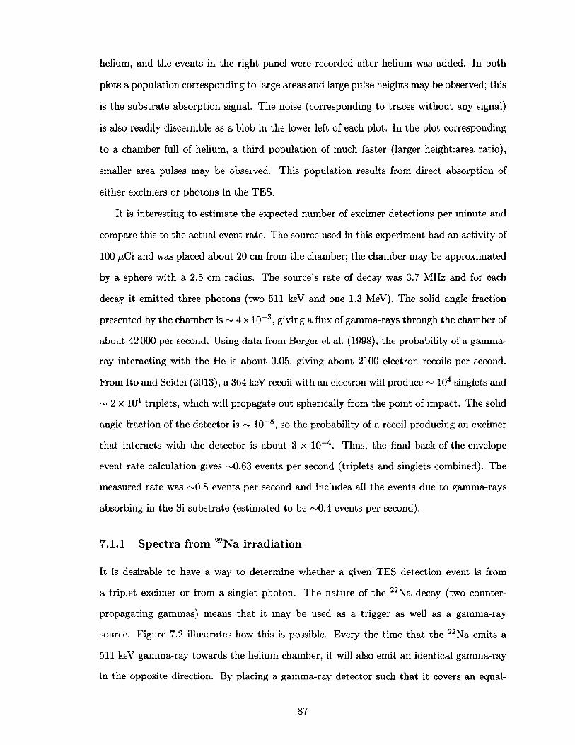
helium, and the events in the right panel were recorded after helium was added. In both
plots a population corresponding to large areas and large pulse heights may be observed; this
is the substrate absorption signal. The noise (corresponding to traces without any signal)
is also readily discernible as a blob in the lower left of each plot. In the plot corresponding
to a chamber full of helium, a third population of much faster (larger height:area ratio),
smaller area pulses may be observed. This population results from direct absorption of
either excimers or photons in the TES.
It is interesting to estimate the expected number of excimer detections per minute and
compare this to the actual event rate. The source used in this experiment had an activity of
100 /xCi and was placed about 20 cm from the chamber; the chamber may be approximated
by a sphere with a 2.5 cm radius. The source’s rate of decay was 3.7 MHz and for each
decay it emitted three photons (two 511 keV and one 1.3 MeV). The solid angle fraction
presented by the chamber is ~ 4 x 10~3, giving a flux of gamma-rays through the chamber of
about 42000 per second. Using data from Berger et al. (1998), the probability of a gamma-
ray interacting with the He is about 0.05, giving about 2100 electron recoils per second.
From Ito and Seidel (2013), a 364 keV recoil with an electron will produce ~ 104 singlets and
~ 2 x 10⁴ triplets, which will propagate out spherically from the point of impact. The solid
angle fraction of the detector is ~ 1 0 -8 , so the probability of a recoil producing an excimer
tha t interacts with the detector is about 3 x 10⁻⁴ . Thus, the final back-of-the-envelope
event rate calculation gives ~0.63 events per second (triplets and singlets combined). The
measured rate was ~ 0 . 8 events per second and includes all the events due to gamma-rays
absorbing in the Si substrate (estimated to be ~0.4 events per second).
7.1.1 S p ectra from 22N a irradiation
It is desirable to have a way to determine whether a given TES detection event is from
a triplet excimer or from a singlet photon. The nature of the 22Na decay (two counter-
propagating gammas) means tha t it may be used as a trigger as well as a gamma-ray
source. Figure 7.2 illustrates how this is possible. Every the time tha t the 22Na emits a
511 keV gamma-ray towards the helium chamber, it will also emit an identical gamma-ray
in the opposite direction. By placing a gamma-ray detector such tha t it covers an equal-
87
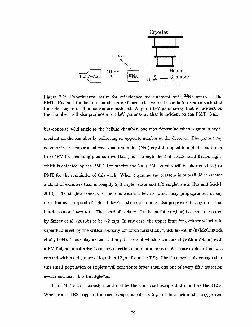
C ryostat
1.3 MeVX/ 511 keV f
PMT+Nal <—------- 22— \ L
Figure 7.2: Experimental setup for coincidence measurement with 22Na source. The PM T+N al and the helium chamber are aligned relative to the radiation source such that the solid angles of illumination are matched. Any 511 keV gamma-ray tha t is incident on the chamber, will also produce a 511 keV gamma-ray tha t is incident on the PM T+N al.
but-opposite solid angle as the helium chamber, one may determine when a gamma-ray is
incident on the chamber by collecting its opposite number at the detector. The gamma ray
detector in this experiment was a sodium-iodide (Nal) crystal coupled to a photo-multiplier
tube (PMT). Incoming gamma-rays tha t pass through the Nal create scintillation light,
which is detected by the PMT. For brevity the N al+PM T combo will be shortened to just
PM T for the remainder of this work. When a gamma-ray scatters in superfluid it creates
a cloud of excimers tha t is roughly 2/3 triplet state and 1/3 singlet state (Ito and Seidel,
2013). The singlets convert to photons within a few ns, which may propagate out in any
direction at the speed of light. Likewise, the triplets may also propagate in any direction,
but do so at a slower rate. The speed of excimers (in the ballistic regime) has been measured
by Zmeev et al. (2013b) to be ~ 2 m /s. In any case, the upper limit for excimer velocity in
superfluid is set by the critical velocity for roton formation, which is ~50 m /s (McClintock
et al., 1984). This delay means tha t any TES event which is coincident (within 250 ns) with
a PM T signal must arise from the collection of a photon, or a triplet state excimer tha t was
created within a distance of less than 12 fim from the TES. The chamber is big enough tha t
this small population of triplets will contribute fewer than one out of every fifty detection
events and may thus be neglected.
The PM T is continuously monitored by the same oscilloscope tha t monitors the TESs.
Whenever a TES triggers the oscilloscope, it collects 5 / i s of data before the trigger and
511 k<?V .
HeliurhC ham ber
88
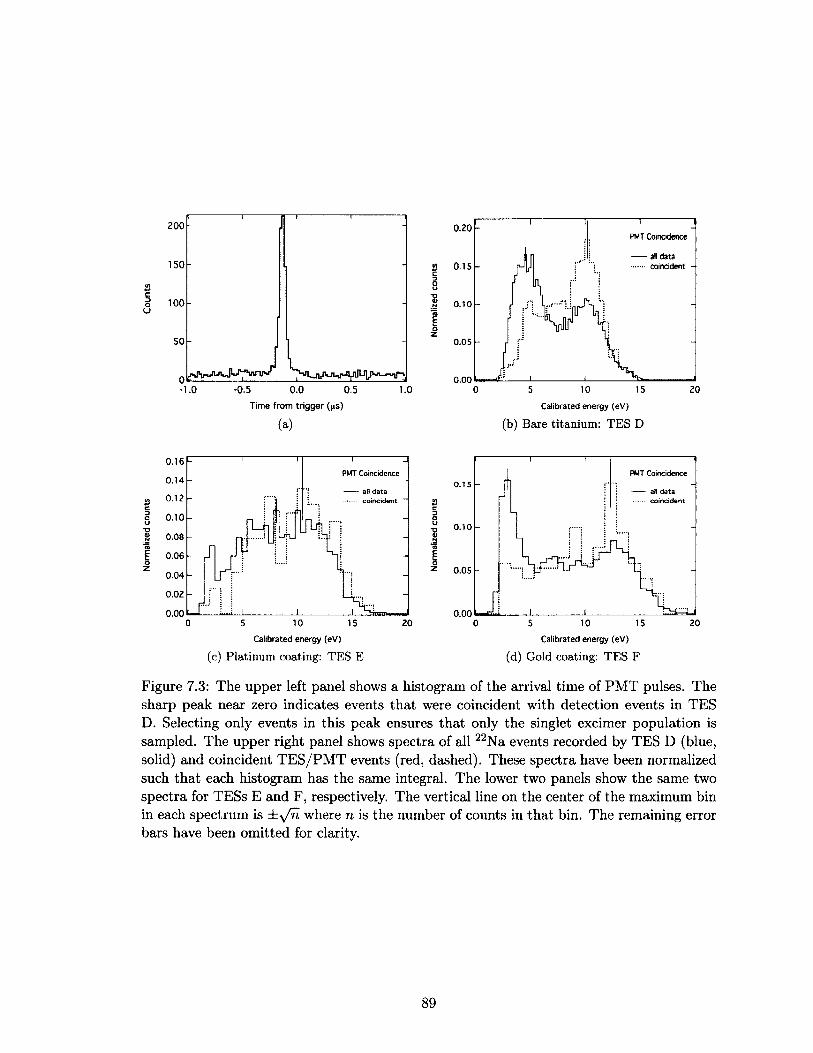
200
150
1 0 0
SO
- 1.0 -0.5 0.0 0.5 1.0Time from trigger (us)
(a)
0.20PMT Coincidence
all data coincident -0 .15<0C3oo
0.10re§oz
0 .0 5
0.0010 200 5 15
Calibrated energy (eV)(b) Bare titanium: TES D
PMT Coincidence0 .15
ail d a ta co in c id en t
0.10
0 .0 5
0.000 5 10 15 20
0 .1 6PMT Coincidence
0 .1 4all d a ta co in c id en t0.12
0.10 -
0 .0 8
0 .0 6
0 .0 4
0.02
0.000 5 10 15 2 0
Calibrated energy (eV) Calibrated energy (eV)(c) Platinum coating: TES E (d) Gold coating: TES F
Figure 7.3: The upper left panel shows a histogram of the arrival time of PM T pulses. The sharp peak near zero indicates events tha t were coincident with detection events in TES D. Selecting only events in this peak ensures tha t only the singlet excimer population is sampled. The upper right panel shows spectra of all 22Na events recorded by TES D (blue, solid) and coincident TE S/PM T events (red, dashed). These spectra have been normalized such tha t each histogram has the same integral. The lower two panels show the same two spectra for TESs E and F, respectively. The vertical line on the center of the maximum bin in each spectrum is ±^/n where n is the number of counts in tha t bin. The remaining error bars have been omitted for clarity.
89
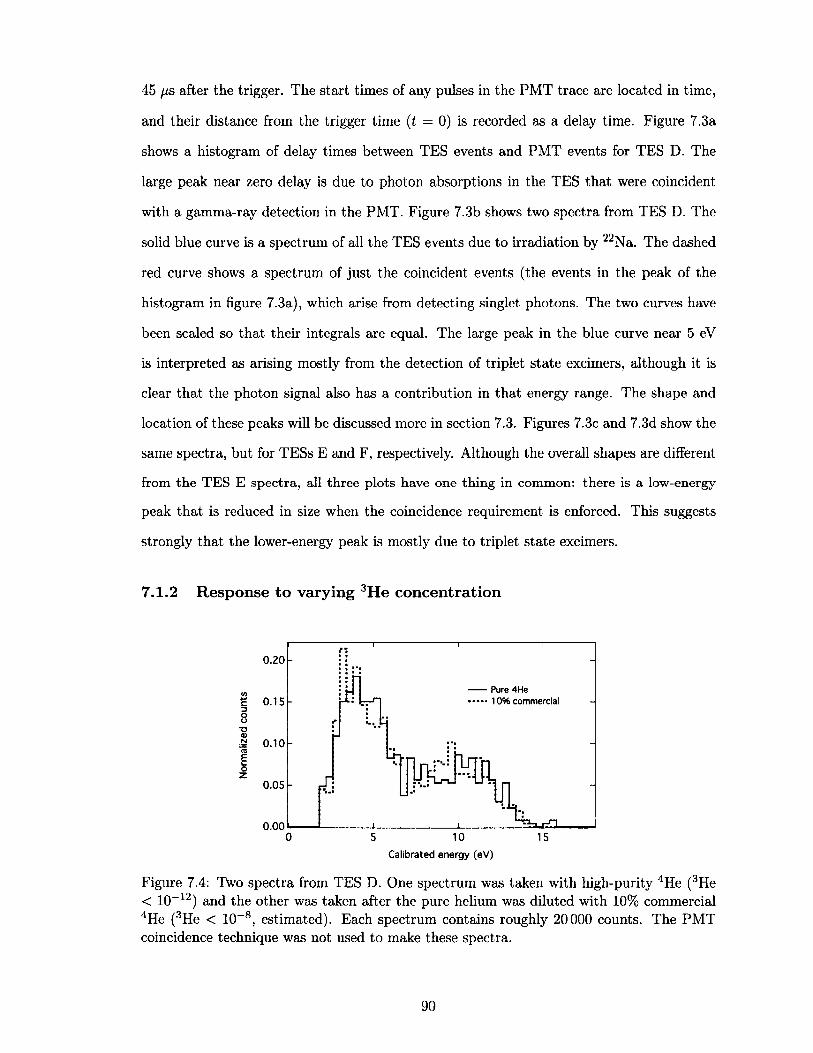
45 fj,s after the trigger. The start times of any pulses in the PM T trace are located in time,
and their distance from the trigger time (t = 0) is recorded as a delay time. Figure 7.3a
shows a histogram of delay times between TES events and PM T events for TES D. The
large peak near zero delay is due to photon absorptions in the TES tha t were coincident
with a gamma-ray detection in the PMT. Figure 7.3b shows two spectra from TES D. The
solid blue curve is a spectrum of all the TES events due to irradiation by 2 2 Na. The dashed
red curve shows a spectrum of just the coincident events (the events in the peak of the
histogram in figure 7.3a), which arise from detecting singlet photons. The two curves have
been scaled so tha t their integrals are equal. The large peak in the blue curve near 5 eV
is interpreted as arising mostly from the detection of triplet state excimers, although it is
clear tha t the photon signal also has a contribution in tha t energy range. The shape and
location of these peaks will be discussed more in section 7.3. Figures 7.3c and 7.3d show the
same spectra, but for TESs E and F, respectively. Although the overall shapes are different
from the TES E spectra, all three plots have one thing in common: there is a low-energy
peak tha t is reduced in size when the coincidence requirement is enforced. This suggests
strongly tha t the lower-energy peak is mostly due to triplet state excimers.
7.1 .2 R esp on se to varying 3H e con cen tration
0.20
Pure 4He 10% commercial0 .1 5
0.10
0 .0 5
0.000 5 1 0 15
Calibrated energy (eV)
Figure 7.4: Two spectra from TES D. One spectrum was taken with high-purity 4He (3He < 1 0 -12) and the other was taken after the pure helium was diluted with 1 0 % commercial 4He (3He < 10-8 , estimated). Each spectrum contains roughly 20000 counts. The PM T coincidence technique was not used to make these spectra.
90
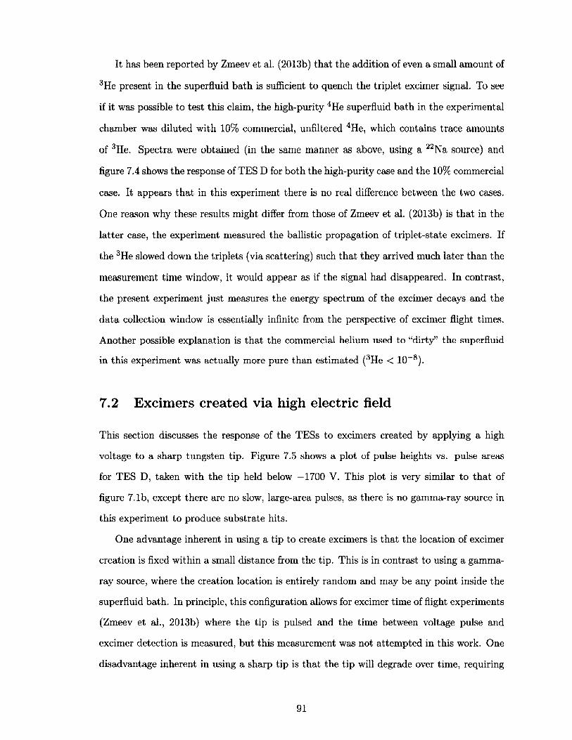
It has been reported by Zmeev et al. (2013b) tha t the addition of even a small amount of
3He present in the superfluid bath is sufficient to quench the triplet excimer signal. To see
if it was possible to test this claim, the high-purity 4He superfluid bath in the experimental
chamber was diluted with 10% commercial, unfiltered 4 He, which contains trace amounts
of 3 He. Spectra were obtained (in the same manner as above, using a 22Na source) and
figure 7.4 shows the response of TES D for both the high-purity case and the 10% commercial
case. It appears tha t in this experiment there is no real difference between the two cases.
One reason why these results might differ from those of Zmeev et al. (2013b) is tha t in the
latter case, the experiment measured the ballistic propagation of triplet-state excimers. If
the 3He slowed down the triplets (via scattering) such tha t they arrived much later than the
measurement time window, it would appear as if the signal had disappeared. In contrast,
the present experiment just measures the energy spectrum of the excimer decays and the
data collection window is essentially infinite from the perspective of excimer flight times.
Another possible explanation is tha t the commercial helium used to “dirty” the superfluid
in this experiment was actually more pure than estimated (3He < 10-8 ).
7.2 Excimers created via high electric field
This section discusses the response of the TESs to excimers created by applying a high
voltage to a sharp tungsten tip. Figure 7.5 shows a plot of pulse heights vs. pulse areas
for TES D, taken with the tip held below —1700 V. This plot is very similar to tha t of
figure 7.1b, except there are no slow, large-area pulses, as there is no gamma-ray source in
this experiment to produce substrate hits.
One advantage inherent in using a tip to create excimers is tha t the location of excimer
creation is fixed within a small distance from the tip. This is in contrast to using a gamma-
ray source, where the creation location is entirely random and may be any point inside the
superfluid bath. In principle, this configuration allows for excimer time of flight experiments
(Zmeev et al., 2013b) where the tip is pulsed and the time between voltage pulse and
excimer detection is measured, but this measurement was not attem pted in this work. One
disadvantage inherent in using a sharp tip is tha t the tip will degrade over time, requiring
91
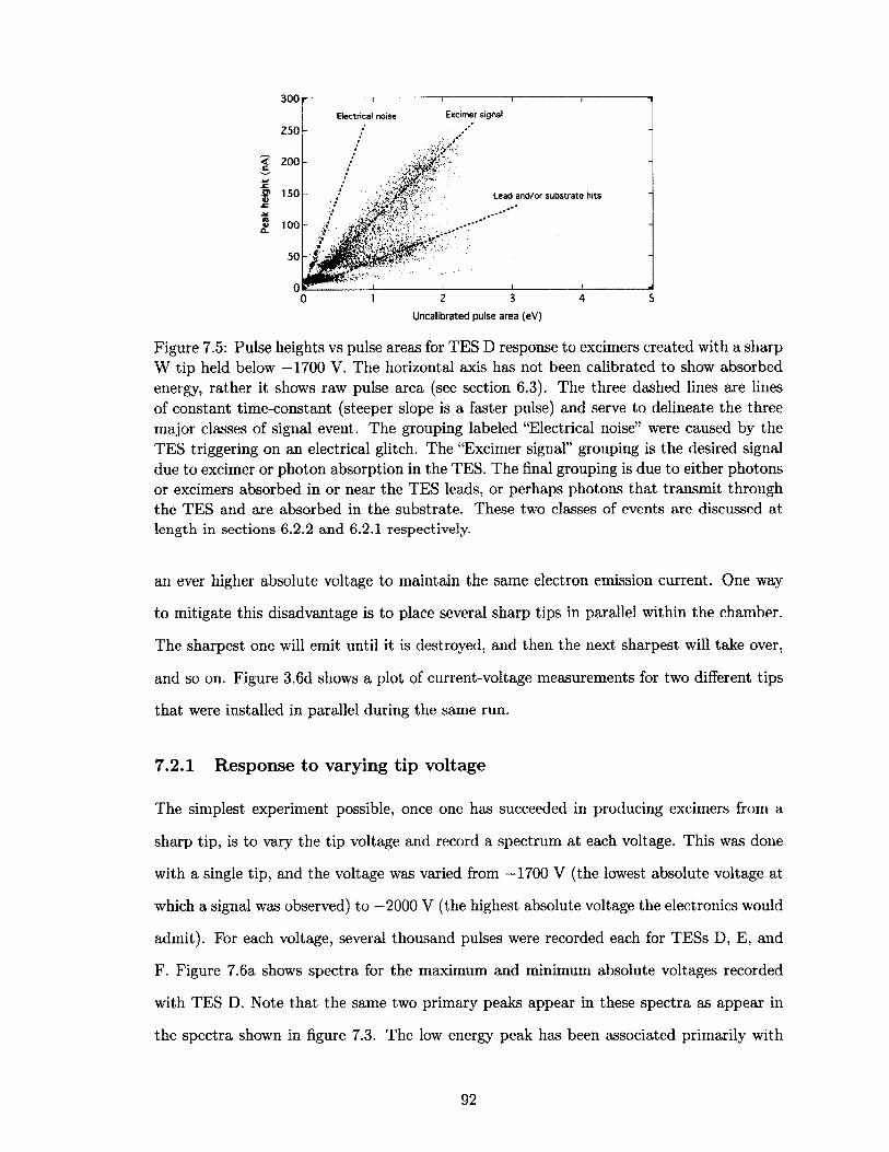
300Excimer signalElectrical noise
200<cXZ0 5C£
150 Lead and/or substra te hits
mvo_ 1 0 0
3 52 40
Uncalibrated pulse area (eV)
Figure 7.5: Pulse heights vs pulse areas for TES D response to excimers created with a sharp W tip held below —1700 V. The horizontal axis has not been calibrated to show absorbed energy, rather it shows raw pulse area (see section 6.3). The three dashed lines are lines of constant time-constant (steeper slope is a faster pulse) and serve to delineate the three major classes of signal event. The grouping labeled “Electrical noise” were caused by the TES triggering on an electrical glitch. The “Excimer signal” grouping is the desired signal due to excimer or photon absorption in the TES. The final grouping is due to either photons or excimers absorbed in or near the TES leads, or perhaps photons tha t transm it through the TES and are absorbed in the substrate. These two classes of events are discussed at length in sections 6 .2 . 2 and 6 .2 . 1 respectively.
an ever higher absolute voltage to maintain the same electron emission current. One way
to mitigate this disadvantage is to place several sharp tips in parallel within the chamber.
The sharpest one will emit until it is destroyed, and then the next sharpest will take over,
and so on. Figure 3.6d shows a plot of current-voltage measurements for two different tips
tha t were installed in parallel during the same run.
7.2.1 R esp on se to varying tip vo ltage
The simplest experiment possible, once one has succeeded in producing excimers from a
sharp tip, is to vary the tip voltage and record a spectrum at each voltage. This was done
with a single tip, and the voltage was varied from —1700 V (the lowest absolute voltage at
which a signal was observed) to —2000 V (the highest absolute voltage the electronics would
admit). For each voltage, several thousand pulses were recorded each for TESs D, E, and
F. Figure 7.6a shows spectra for the maximum and minimum absolute voltages recorded
with TES D. Note tha t the same two primary peaks appear in these spectra as appear in
the spectra shown in figure 7.3. The low energy peak has been associated primarily with
92
triplet state excimers and the higher energy peak with photon absorption from singlet state
excimer decay. Figure 7.6b shows how these two peak areas vary with increasing absolute
tip voltage: The triplet peak area decreases with increasing absolute tip voltage, while the
singlet peak area increases. Zmeev et al. (2013a) found tha t a tip at high absolute voltage
produces a turbulent vortex tangle as well as excimers. It is possible tha t increasing the
absolute tip voltage increases the amount of turbulence, and thus the number of vortices,
produced in the superfluid at the tip. Since triplet state excimers are efficiently trapped
on vortices, increasing the tip to a higher absolute voltage would effectively reduce the
number of triplet state excimers tha t reach the detector. Another possibility is th a t as the
density of triplet state excimers in the vicinity of the needle increases, they become more
likely to quench on each other through Penning ionization (Shaw, 1974; Adams, 2001), and
eventually are converted to photons, which show up in the higher energy singlet peak. This
process has a reaction rate of ~ 1 0 - 9 cm3 /s , which limits the maximum possible triplet
density (Keto et al., 1974).
Figures 7.6c and 7.6d show the same spectra as figure 7.6a, except for TESs E and F,
which were coated with a thin layer of platinum and gold, respectively. Although the peak
height shift is not as pronounced in these spectra, there is still a shift in peak area from the
low-energy peak to the high-energy peak with increasing absolute voltage, which is in line
with the hypotheses made above regarding the relationship of vortex creation (or Penning
ionization) to tip voltage.
7.3 Discussion
The previous sections in this chapter have presented several spectra, and made claims as to
what the different peaks in the spectra represent (i.e., one is the triplet peak, etc). There
are three outstanding questions tha t immediately ask for resolution.
1. Why is the triplet peak at such a low energy if the excimer binding energy is ~15 eV?
2. Why do the spectrum shapes differ between detectors if they are detecting the same
signal?
93
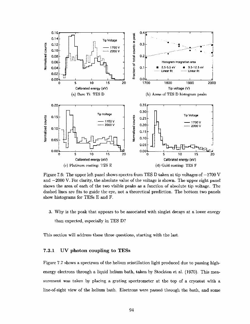
0.16
0.14 Tip Voltage2 0 .1 2c3OO
T 3VN15
1700 V 2000 V0.10
0 .08
0 .06£uOz 0 .04
0.02
0.002010 IS0 5
Calibrated energy (eV)
(a) Bare Ti: TES D
ravac
0.4
0.3
0.2
0.1
0.0 k1700
Histogram integration area
■ 2.5-5.5 eV • 9.5-12.5 eV Linear fit Linear fit
1800 1900
Tip voltage (V)
(b) Areas of TES D histogram peaks
2000
0.35
0 .30</>c 0.25 => o0 TJ V
1 0.15 (0
§ o.io z
0.05
Tip Voltage
1700 V 2000 V0.20
0.000 5 1 0 2015
0.20
Tip Voltage(A 0.15c3oo 1700 V
2000 V0.10vM
nEl.oz 0.05
0.00 L 0 10 205 15
Calibrated energy (eV) Calibrated energy (eV)
(c) Platinum coating: TES E (d) Gold coating: TES F
Figure 7.6: The upper left panel shows spectra from TES D taken at tip voltages of —1700 V and —2000 V. For clarity, the absolute value of the voltage is shown. The upper right panel shows the area of each of the two visible peaks as a function of absolute tip voltage. The dashed lines are fits to guide the eye, not a theoretical prediction. The bottom two panels show histograms for TESs E and F.
3. Why is the peak tha t appears to be associated with singlet decays at a lower energy
than expected, especially in TES D?
This section will address these three questions, starting with the last.
7.3 .1 U V p h oton cou p lin g to T E Ss
Figure 7.7 shows a spectrum of the helium scintillation light produced due to passing high-
energy electrons through a liquid helium bath, taken by Stockton et al. (1970). This mea
surement was taken by placing a grating spectrometer at the top of a cryostat with a
line-of-sight view of the helium bath. Electrons were passed through the bath, and some
94
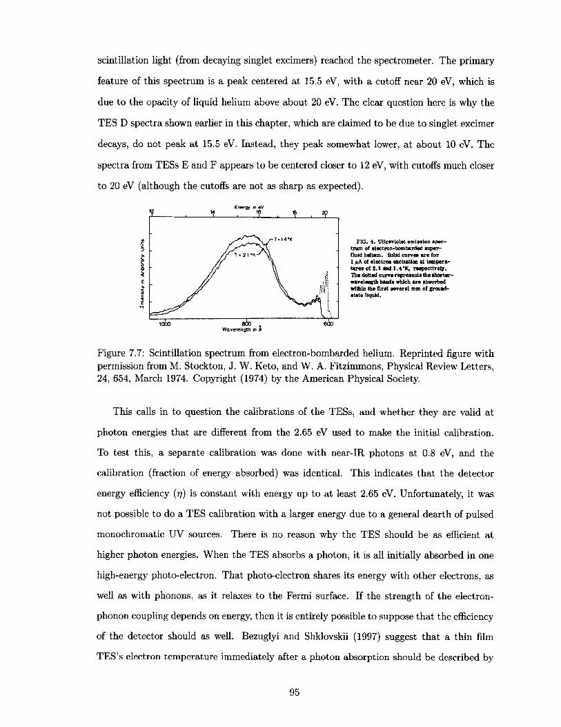
scintillation light (from decaying singlet excimers) reached the spectrometer. The primary
feature of this spectrum is a peak centered at 15.5 eV, with a cutoff near 20 eV, which is
due to the opacity of liquid helium above about 20 eV. The clear question here is why the
TES D spectra shown earlier in this chapter, which are claimed to be due to singlet excimer
decays, do not peak at 15.5 eV. Instead, they peak somewhat lower, at about 10 eV. The
spectra from TESs E and F appears to be centered closer to 12 eV, with cutoffs much closer
to 2 0 eV (although the cutoffs are not as sharp as expected).
FIG. 4. Ultraviolet emission spectrum of electron-bombarded super- fluid helium. Solid curves are for 1 pA of electron excitation at temperatures of 2.1 and 1.4 *K, respectively. The dotted curve represents the shorter- wavelength bands which are absorbed within the first several mm of ground- state liquid.
Figure 7.7: Scintillation spectrum from electron-bombarded helium. Reprinted figure with permission from M. Stockton, J. W. Keto, and W. A. Fitzimmons, Physical Review Letters, 24, 654, March 1974. Copyright (1974) by the American Physical Society.
This calls in to question the calibrations of the TESs, and whether they are valid at
photon energies tha t are different from the 2.65 eV used to make the initial calibration.
To test this, a separate calibration was done with near-IR photons at 0.8 eV, and the
calibration (fraction of energy absorbed) was identical. This indicates tha t the detector
energy efficiency (77) is constant with energy up to at least 2.65 eV. Unfortunately, it was
not possible to do a TES calibration with a larger energy due to a general dearth of pulsed
monochromatic UV sources. There is no reason why the TES should be as efficient at
higher photon energies. When the TES absorbs a photon, it is all initially absorbed in one
high-energy photo-electron. That photo-electron shares its energy with other electrons, as
well as with phonons, as it relaxes to the Fermi surface. If the strength of the electron-
phonon coupling depends on energy, then it is entirely possible to suppose tha t the efficiency
of the detector should as well. Bezuglyi and Shklovskii (1997) suggest th a t a thin film
TES’s electron temperature immediately after a photon absorption should be described by
T » U K
5
c>3ccM
6001000W avelength n A
95
-E'phot = V 7 / 2 ( T | e s - T Eath). In limit of (T t e s - Tbath) «C Tbath, this reduces to
£phot = t/ 7 Tbath (rTES - Tbath) or, more familiarly, E’phot = CeATTES. However, at larger
input energies, the TES electron temperature rises like the square-root of the photon energy.
In this case, treating the detector temperature as linear with regards to photon energy will
result in an underestimate of the true photon energy. As an example, for E phot = 15 eV,
Tbath = 100 mK, V = 1 /tm3, and 7 = 304 J /K 2 m3, the above equation predicts a measured
energy of 13.4 eV, or about a 12% discrepancy.
At higher photon energies (larger than the work function of the TES), the photo-electric
effect also may play a role. When an electron is removed from the TES via the photo
electric effect, the resulting hole is filled by an electron at the Fermi-surface, and the energy
difference is read out as a pulse on the oscilloscope. This means tha t, in addition to a
peak around 15.5 eV, a TES tha t measures UV light should also have some peaks at lower
energies tha t correspond to the TES band structure within several eVs of the Fermi level.
Oxidized titanium has a large peak in the density of states tha t is 5 eV below the Fermi
level (Eastman, 1972; Hanson et al., 1981; Hagstrom et al., 1977). This is one possible
explanation for why, in figure 7.3, even after using the PM T to window exclusively on the
photon signal, there are still many counts near 5 eV.
The spectra from TESs E and F are closer to what is expected at high energies in the
sense tha t the cutoff is closer to tha t expected from figure 7.7. One possible reason for
this is tha t the extra layer of metal present on these two TESs helps keep the efficiency
more constant at higher energies, as any high-energy phonons created during the initial
photo-electron’s scattering process will have a higher probability of being reabsorbed into
the electron system thanks to the larger total detector volume.
7.3.2 Triplet excimer coupling to TES
Figure 7.8 depicts the manner in which a triplet excimer couples its energy to the TES.
This has been generalized from the method in which a single excited He atom couples to a
surface presented by Harada et al. (1997). There are four main steps:
1 . When the excimer gets physically close to the TES surface, the excited electron res-
96
onantly tunnels into the empty states above the Fermi level. This electron scatters
down to the Fermi surface, releasing an energy (E\ - Ep) into the TES. For this to
happen, the work function of the TES surface must be greater than Ev — E\. E\ is
somewhat dependent on the proximity of the excimer to the surface, and increases as
this distance decreases.
2. An electron from within the TESs Fermi sea fills the empty state at the ground level
of the helium atom, leaving a hole in the TES Fermi sea.
3. An electron from within the Fermi sea gains the energy released in the previous step
( £ 3 — Eg) through an Auger process. This may be enough energy to cause the electron
to escape the TES.
4. Finally, electrons from the Fermi surface drop down to fill the holes left in the previous
two steps. These two energies are Ep — £ 3 and Ep — £ 2 - If the Auger electron
from the previous step remains within the TES, it will deposit the rest of its energy,
( £ 3 — £ g) — (£p — £ 2 ), in the TES as it relaxes to the Fermi level.
In this process, E\ — Ep is always deposited in the TES. For Ti, this energy is very nearly
zero. For Au and P t, it should be about 2-3 eV, as these metals have larger work-functions
than Ti. There appears to be a peak near 2-3 eV in both figure 7.3c and figure 7.3d that
is reduced in size when the triplet signal is suppressed by enforcing PM T coincidence. The
two electrons from steps 2 and 3 can come from any filled state in the TES, and so the
density of states plays a large part in determining £ 2 and £ 3 . There is also no reason why
£ 2 should be larger than £ 3 . This process effectively maps out the density of states near the
Fermi level, and is nearly the inverse of a technique called atomic/molecular deexcitation
spectroscopy (Trioni et al., 2005; Harada et al., 1997). In tha t process the Auger electron is
collected when it escapes from the surface, where in this case, the TES collects the energy
tha t does not escape.
This process gives some insight into the spectra shown in this chapter and allows one
to make some educated guesses as to what the various peaks all mean. The following
statem ents are this author’s best hypotheses as to what is happening, but a more careful
97
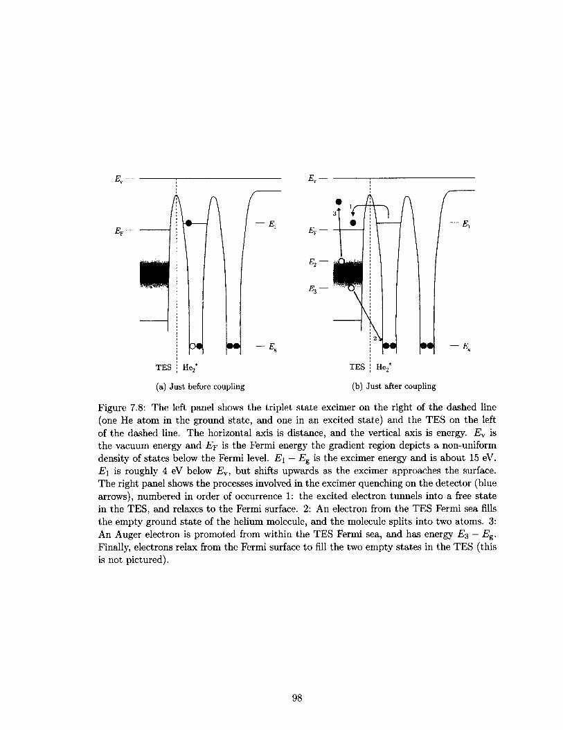
TES
(a) Just before coupling (b) Just after coupling
Figure 7.8: The left panel shows the triplet state excimer on the right of the dashed line (one He atom in the ground state, and one in an excited state) and the TES on the left of the dashed line. The horizontal axis is distance, and the vertical axis is energy. Ev is the vacuum energy and Ep is the Fermi energy the gradient region depicts a non-uniform density of states below the Fermi level. E\ — Eg is the excimer energy and is about 15 eV. Ei is roughly 4 eV below Ev, but shifts upwards as the excimer approaches the surface. The right panel shows the processes involved in the excimer quenching on the detector (blue arrows), numbered in order of occurrence 1 : the excited electron tunnels into a free state in the TES, and relaxes to the Fermi surface. 2: An electron from the TES Fermi sea fills the empty ground state of the helium molecule, and the molecule splits into two atoms. 3: An Auger electron is promoted from within the TES Fermi sea, and has energy £ 3 — Eg. Finally, electrons relax from the Fermi surface to fill the two empty states in the TES (this is not pictured).
98
study with higher energy resolution is required to make any definitive statements.
Discussion of TES D spectra
Oxidized titanium (and TES D is certainly oxidized as it was exposed to air for several days
prior to installation) has peaks in the density of states near 2 eV and 5 eV below the Fermi
level (Eastman, 1972; Hanson et al., 1981; Hagstrom et al., 1977). This means tha t when
the Auger electron escapes, there should be peaks in the spectrum at 4 ( 2 + 2 ), 7 ( 2 + 5,
5 + 2), and 10 (5 + 5) eV, and when the Auger is reabsorbed there will be a peak near 15 eV
as in tha t case, the to tal energy of the excimer is deposited in the TES. The blue curve from
figure 7.3b has a broad peak at 4 eV tha t shifts to a narrower peak at 5 eV when the PM T
coincidence is applied (red curve). This is the expected behavior as the dominant physics
for the low energy-peak on the red curve should be the photo-electric effect as discussed
above in section 7.3.1.
Discussion of TES E spectra
The density of states of platinum has a sharp narrow peak within an eV of the Fermi level,
but then is relatively constant below 1 eV (Harada et al., 1997; Baptist and Chauvet, 2000).
This explains the lack of any real structure in the TES E spectra depicted in figure 7.3c save
for the small peak near 2 eV, which is likely due to the fact tha t E\ « 2 eV for platinum.
This peak is strongly reduced when PM T coincidence is enforced, as expected.
Discussion of TES F spectra
The density of states of gold has a large peak near 3 eV below the Fermi level (Krolikowski
and Spicer, 1970; Smith, 1971), which should give rise to a peak in the blue curve of
figure 7.3d at 6 eV (3 + 3). There does appear to be a small bump in the spectrum near
6 eV, but that could also be due to statistical variation. The large peak near 3 eV is due
to triplet excimers, as may be seen by the corresponding reduction of tha t peak in the red
curve. The most plausible origin of this peak is that, like platinum, E\ is about 2 eV for
gold and so the spectrum is peaked at low energy.
99

Discussion o f TES count rate differences
It is clear from the sizes of the error bars on the blue curves in figure 7.3 tha t the TES D
spectrum contains many more counts than the spectra collected by either TES E or TES
F. The reason for this is unknown. The fact tha t both TES E and F experienced the same
dearth of detection events when exposed to the same excimer flux suggests tha t the surface
chemistry is responsible; gold and platinum both have similar surface properties. For now
this will have to remain an open question.
100
Next steps QChapter
Sh o r t l y before the writing of this dissertation, the experiment was decommissioned and
is, at the time of this writing, bound for the University of California, Berkeley. In
the hopes tha t it may be eventually recommissioned, here are presented a number of things
tha t could be done differently (and better). W ith a better system would come increased
capabilities to answer questions, and so a list of future science goals is also presented.
8.1 Engineering improvements for version 2
This section breaks down the list of improvements tha t ought to be made to any future
version of this experiment by sub-system.
8.1 .1 E lectron ics
Low-voltage signal electronics
There were three main issues encountered with the signal electronics.
1 . The original detector design (discussed in appendix A) called for a two-pixel TES
coupled to an aluminum absorber tha t also acted as a shared ground. Unfortunately,
the bias current sources provided with the SQUID system tha t was purchased for this
experiment was not able to provide two independent current biases when two of the
SQUID chips were sharing a ground.
2. There was no way to attach external instruments to the SQUID/TES system. It
would have been helpful to be able to measure the complex impedance of the TESs
as a function of a frequency, but there were no ports for applying an external signal
to the TES.
3. The TES was very sensitive to any small currents on the ground lines. Turning the
room lights on/off, connecting a new instrument, rolling a large metal object near the
cryostat, or even using a noisy switched-mode computer power supply were all enough
to introduce fluctuations in the TES output tha t were several times larger than the
photon signal.
All three of these problems are easily remedied, and only require some careful planning
when wiring up the electronics for the first time. First, each twisted pair/trip let should
have its own shield (either a braided stainless steel sheath or a solid thin-walled stainless
steel capillary). At each stage of the cryostat, all the output lines should be filtered heavily
with non-dissipative low-pass filters at the desired bandwidth. The input lines should have
current dividers at each cryostat stage to reduce the input fluctuations by several orders of
magnitude. Care should be taken, however, not to attenuate so much tha t the input current
source is incapable of biasing the TES. Second, instead of using the built-in current sources,
the input lines should instead be wired to general input ports at the cryostat bulkhead.
This would allow one to connect anything from a current source to a spectrum analyzer to
the TES, and would make it easy to take measurements of the complex impedance as well
as the Jb/TrES curves. Finally, it is now clear tha t there was really no need to mount the
SQUID amplifiers in the same chamber as the TES. Originally this was done to minimize the
parasitic resistance (see figure 2.2). A better design would have had each SQUID amplifier
in its own niobium shield, mounted outside the chamber on the cryostat baseplate.
102
High-voltage tip electronics
The main difficulty with the HV system was figuring out a way to create a high-voltage
pulse tha t was short (~ /zs) and did not produce any electrical noise tha t would be picked up
by the TES. This was never properly solved. The answer is probably to spend some money
and just buy a system engineered for exactly this. They exist, but are expensive. Attempts
to build one from scratch were only marginally successful; it produced a short high-voltage
pulse, but also produced so much electronic noise tha t it completely overwhelmed the TES.
The HV system was also slightly more complicated than was necessary, as it included
a grid at a negative high-voltage to keep electrons from the tip from impacting the TES.
However, by the time they reach the TES the energy contained in any electrons is below
the noise floor of the detector. During this experiment, there was no observed difference in
signal whether the high-voltage grid was on or off.
8.1 .2 LH e cham ber
The chamber discussed in chapter 3 has several flaws tha t a new chamber design could
address.
1. The chamber is very large. It takes 100 L of helium gas at standard temperature and
pressure to fill it up completely with superfluid helium. The condensation process
takes a very long time, and the more helium required to fill the chamber, the more
potential there is for an ice block in the filling capillary.
2. Opening and closing the chamber was a laborious process due to the large number
of screws required to seal the flange. It was also very difficult to access the tungsten
needles, which needed to be changed after every cool-down. The more difficult a
subsystem is to access, the more likely it will be broken whenever maintenance is
required.
3. There were far too many electrical lines going into the chamber. As discussed above,
the choice to mount the SQUIDs inside the chamber was not a particularly good one
and raised the number of required DC feedthroughs into the chamber from 6 to 24.
103
An extra 25-pin connector was also added for auxiliary wiring. This connector was
never used, and could have been eliminated.
4. The lack of a film-burner meant tha t a small injection capillary had to be used for
helium filling in order to minimize the heat leak from the superfluid film. Because
such a small capillary was prone to ice blockages, a secondary plumbing line had to
be added to the chamber to evacuate it sufficiently fast in the event of either a rapid
unscheduled warm up or a capillary ice blockage. This secondary plumbing line, while
necessary (it was required more than once), could be eliminated by incorporating
a film burner and using a larger injection line. If a supplier could be found, this
simplification would be well worth any added cost. One possible option would be to
salvage a still unit off of a decommissioned dilution refrigerator (or convince a cryostat
company to sell a stand-alone still), as the film burner is typically incorporated into
the still.
5. The “high voltage” feedthroughs used were actually RF feedthroughs and were only
good to about 1800 V. It would have been much better to use true high-voltage
feedthroughs (and would have saved the hassle of having to replace them).
The solution to most of the above issues is simple: redesign the chamber to be cylindrical
with a circular flange on each end. One flange could hold the detectors along with two DC
feedthroughs per TES (as mentioned above, the SQUIDs would be outside the chamber in
this implementation). The other flange could hold all the tungsten needle hardware, the
fiber-optic feedthrough, and the helium injection port. Either flange could be mounted with
no more than six bolts and would be easily removable for maintenance. Furthermore, only
the system requiring maintenance would have to be removed. The overall volume of helium
required to fill such a chamber could be reduced by a factor of at least two or three without
any special consideration, and perhaps even farther with a careful approach to design.
8.1 .3 T ES
Although the TESs used in this work were sufficient to detect individual excimers, there
are a few improvements tha t could make them much better.
104
1. The TESs could be much thicker. The TESs were 16 nm thick evaporated Ti. As
mentioned in chapter 6 , they were ~20% transparent to both blue light and UV light.
A thicker TES would allow for more complete absorption of signal in the detector.
2. The TESs could be longer. A longer TES (length between leads) would be less sus
ceptible to edge-hits (where the photon is absorbed near enough to the lead tha t it
loses some fraction of the signal to the lead). In chapter 6 it was estimated tha t an
area of about 3 /rm from the leads shouldn’t be used as a detection area as energy
deposited in tha t zone may be lost. A narrow, but long detector would minimize the
effect of edge-hits. Increasing length and thickness is also going to decrease sensitivity,
as the amount of TES heating is proportional to the TES volume, through the heat
capacity, and so there is some limit to how long is reasonable. Another way to reduce
the edge hit effect would be to use a superconductor with a larger Tc (like Nb) for the
leads, which would increase the depth of the hot electron trap. This would come at
the expense of a more complicated fabrication procedure.
3. It might be interesting to consider suspending the TESs above the Si substrate (this
could be accomplished with a Xe2 F etch prior to the aluminum etch tha t exposes the
TES). This would reduce any substrate absorptions and would likely clean the signal
up quite a bit. This is, however, at odds with the above recommendation to make the
TES longer (longer things axe harder to suspend), but would be relatively easy to try.
The robustness of a suspended thin film is not known, but could also prove to be an
issue.
8.2 Future science goals
Here is a short list of immediate goals tha t should be the first priority for a future TES-based
excimer detection experiment.
• Acquire a narrow-band pulsed light source in the vacuum UV (or as high energy as
possible) and look at calibrations over a wide spectrum. This will help determine
whether the efficiency of the TES is constant, or depends on input energy.
105
• It would be interesting to look at more surface materials than just gold or platinum
to get a better idea of what is happening with the excimer coupling, especially with
regards to the count rate.
• A careful look at spectra at a range of different bath temperatures would be very
interesting for both for the tip data and the 22Na data.
• Using an alpha source mounted very near the TES would change the ratio of sin-
glet:triplet excimers produced and would also increase the count rate to the point
where it should be possible to see coincident singlets and triplets tha t arise from the
same scattering event. This would make it possible to determine excimer time-of-flight
as well.
• A low-noise fast HV pulse generator would make time-of-flight measurements using the
tungsten tip possible, and would make it feasible to actually start studying quantum
turbulence.
• Getting the two-pixel device working would significantly increase the detector col
lection area. There is no reason why this concept should not work, however, the
aluminum absorber should probably be deposited via evaporation, not sputtering, in
order to realize long quasiparticle lifetimes and a large diffusion constant.
8.3 Concluding remarks
This experiment was designed as a proof of concept to show that
1. It is possible to detect individual He^ excimers directly within a superfluid bath.
2. It is possible to differentiate between the triplet and singlet state excimers.
3. It is possible to have a detector tha t is easily scalable to large surface area.
On the first count the experiment was very successful; the detection of individual excimers
has been conclusively demonstrated. Indeed, this work is the first demonstration of calori-
metric detection of individual He^ excimers. On the second count of differentiating between
106
excimer states, the success level was somewhat mixed. It appears tha t each excimer state
has a characteristic spectrum (that also depends strongly on the TES surface material),
but the singlet and triplet spectra overlap in energy to such an extent tha t it is only pos
sible to fully differentiate between the two states in aggregate. Perfect real-time tagging of
individual detection events has not been accomplished. On the third count, there was no
demonstration of detector scalability, but this was not due to any intrinsic limitations of
the detector design. In fact, the success of the single pixel TESs suggests th a t a scalable
detector based on an aluminum absorber should work as designed.
Finally, there is a considerable amount of uncertainty as to the physics behind the unique
spectrum shapes presented in chapter 7. A hypothesis has been put forward that appeals
to the photoelectric effect, the surface chemistry of the TES, and the unknown high-energy
electron-phonon coupling of the TES, but it is not at all rigorous. A full understanding is
not possible within the limits of the current data, and a new set of experiments and devices
is required to arrive at a satisfactory explanation of the results presented here.
107
TES absorber ZAdiffusion math IT * .
Appendix
IMAGINE a long superconducting absorber of superconducting gap energy (A) with TES
detectors at each end. If the TES is biased on the transition, then its superconducting
energy gap is zero, and any quasiparticles at the boundary of the absorber and the TES
will scatter into the lower-energy region of the TES. In the event of a photon incident on
the absorber, the photon will break a Cooper pair and create two excited quasiparticles. As
these quasiparticles relax, they will break more Cooper pairs, exciting more quasiparticles
above the gap, until all the quasiparticles have energy A. These quasiparticles will then
diffuse along the absorber until they reach one of the two TES detectors, where they will
relax down to the Fermi levels of the TESs and will effectively become trapped. They will
share their energy with the electron systems of the two TESs, which will result in a pulse in
each TES. The following analysis solves for the total number of quasiparticles collected by
each of the two detectors as a function of excitation location along the absorber. In sections
A .l and A.2 the lossless 1 -D case is treated. Section A.3 deals with the addition of loss
in the absorber. Section A.4 considers the 2-D case and shows tha t if the boundaries not
connected to the TESs exhibit specular reflection, the problem reduces to the 1-D problem.
Finally, in the last section, section A.5, the addition of a finite trapping length (the distance
a quasiparticle must travel into the TES to become trapped) in the TES is considered and
the result is the conclusion of this appendix. These solutions may also be used to estimate
the number of quasiparticles tha t end up in the TES when a photon is absorbed in/near
the TES leads for the case where the TES lead is a superconductor with a higher Tc than
the TES material.
This problem is well studied already in the context of superconducting tunnel junction
(STJ) detectors and the solution has been presented in multiple works (Loidl et al., 2001; Li,
2003). However, although these works provide the final expression given in (A.34), none of
them (even in aggregate) provide all the steps for arriving at the solution. The full solution
is thus presented here.
A .l Diffusion equation
In 1 -D, the relevant equation for describing the number-density of quasiparticles as a func
tion of time and position is the lossless diffusion equation:
d_dt
$qp(x, t) = ^ (^D (x ) -^% p(x, t)^ (A .l)
If the superconducting absorber is homogeneous along its length, then D(x) — D and the
above becomes:
d ^= ^ ^ 2 >qp(a;’ *) (A-2)
If one assumes tha t $ qp is separable in both time and space1, then $qp(x,t) — X(x)T(t) .
This may be substituted into (A.2) and rearranged to get:
The only way tha t the above equation is valid for all t and all x is if both sides equal some
constant value k. Now the partial differential equation (A.2) has reduced to two ordinary
1. The proof of separability is straightforward: If one is able to separate it, then it is separable. If it is not separable, then it will be impossible to arrive at a separated expression such as (A.3).
109
differential equations:
X"(x) = ~ X { x ) (A.4)
T(t) = kT(t) (A.5)
The solutions to each of these equations are trivial, but depend of the value of the
constant k, which can be positive, negative, or zero. In order to fix the constant, one must
consider the boundary conditions. Let the 1-D wire be centered at x = 0 with length L. As
the quasiparticles diffuse to the end of the wire, they are trapped in the TES and disappear
from the wire; at the ends of the wires, the quasiparticle density must be zero:
X ( ± | ) = 0 (A.6 )
If one considers the solution to (A.4) in light of this boundary condition, there is only one
range of k th a t gives meaningful results: k < 0. In light of this, redefine k -» —k2 where
now k > 0, and rewrite (A.4) and (A.5) as:
X"{x) = = l f x ( x ) (A.7)
T(t) = —k2T(t) (A.8 )
and the solutions to these equations are:
X(x) = Aei:$B + B e^V B (A.9)
T(t) = Ce~kH + Eekh (A. 10)
110
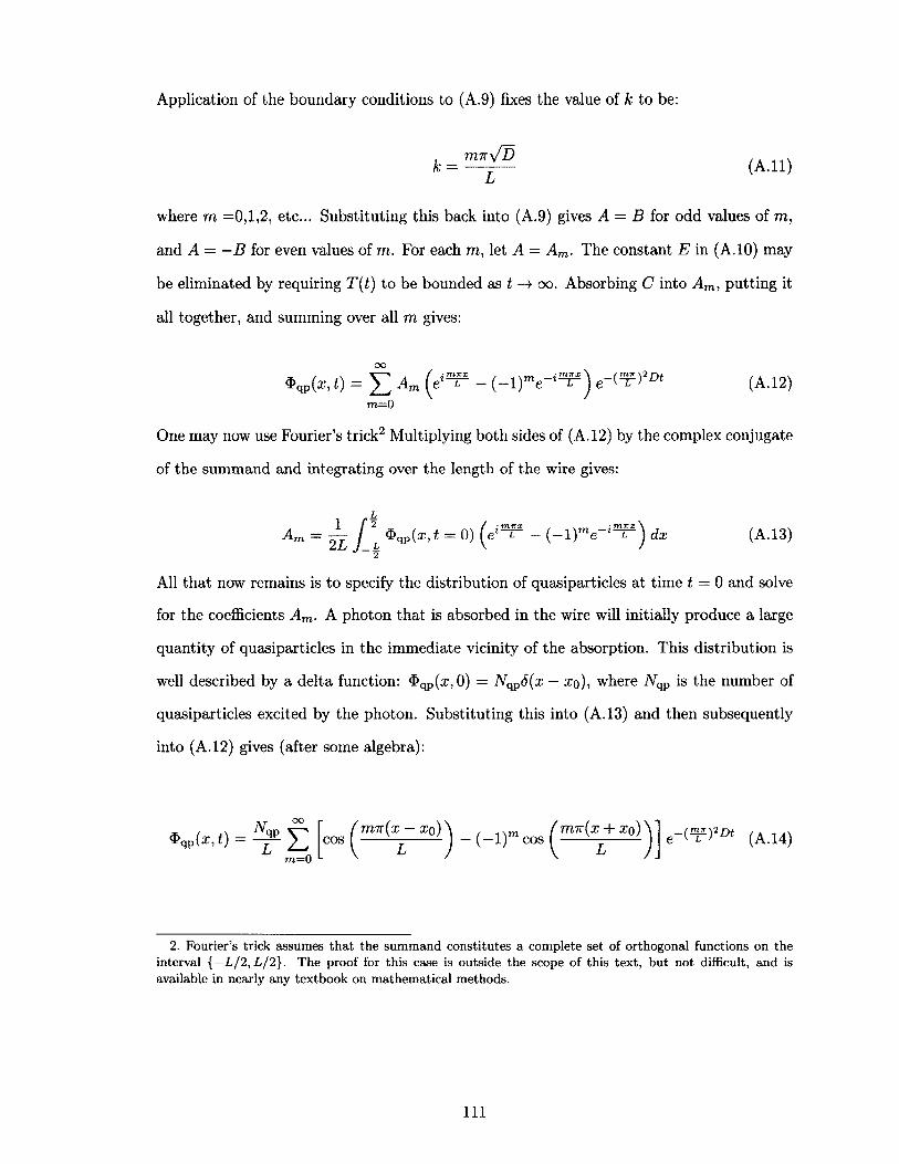
Application of the boundary conditions to (A.9) fixes the value of k to be:
(A.11)
where m =0,1,2, etc... Substituting this back into (A.9) gives A = B for odd values of m,
and A = - B for even values of m. For each m, let A = Am. The constant E in (A.10) may
be eliminated by requiring T( t ) to be bounded as t —»• oo. Absorbing C into A m, putting it
all together, and summing over all m gives:
O O
$ , p(x, t) = £ (e1™ - M r e - ^ ) * -< ¥> ’«• (A.12)m=0
One may now use Fourier’s trick2 Multiplying both sides of (A.12) by the complex conjugate
of the summand and integrating over the length of the wire gives:
Am = 2 ~L J l = 0 ) - ( - 1 )me~%mTr dx (A.13)
All tha t now remains is to specify the distribution of quasiparticles at time t = 0 and solve
for the coefficients Am. A photon tha t is absorbed in the wire will initially produce a large
quantity of quasiparticles in the immediate vicinity of the absorption. This distribution is
well described by a delta function: $qP(x, 0) = Nqp5(x — xq), where Arqp is the number of
quasiparticles excited by the photon. Substituting this into (A.13) and then subsequently
into (A.12) gives (after some algebra):
s ^ . t ) = f ; [cos j _ (_ ir c o s + e- (T m (AJ4)TO=0 f '
2. Fourier’s trick assumes that the summand constitutes a complete set of orthogonal functions on the interval { —L / 2 , L /2 } . The proof for this case is outside the scope of this text, but not difficult, and is available in nearly any textbook on mathematical methods.
I l l
A.2 Solving for the number of quasiparticles in the TES de
tector
In the previous section the quasiparticle number density as a function of time and position
was calculated, given some initial excitation of quasiparticles at xq. W hat is more interesting
is determining the number of quasiparticles tha t end up in each detector after an excitation.
Since the quasiparticles tha t reach the ends of the absorber are trapped into the TESs, the
change in quasiparticle density a t either end of the wire is proportional to the rate at
which quasiparticles get trapped as a function of time (Jn±)- Another way of saying this is
tha t the number current (Jn±) is proportional to the gradient of the number density along
the wire, with the diffusion constant playing the analog of conductivity as the constant of
proportionality.
In the above equation, the absolute value signs account for the fact tha t the change in
magnitude is im portant). The plus sign denotes the TES at x — L /2 and the minus sign
denotes the TES at x = -L /2 . Evaluating this gives:
Finally, this expression may be integrated from the absorption of the photon at time
t = 0 to t —> oo to get the total number of quasiparticles deposited in the TES detector a
long time after an absorption event:
(A-15)
number at the ends may be negative (i.e., the number current has a direction and only the
OO |- ,m n sin I
rr» = n - '
±TO7T m TTXo
2 L^ - (—l) m sin
±m7r mnxo ( 2 2 2 ) 2 D t
(A.16)
±rmr rmrxo2 L
^ — (—l) m sinmirxo
(A.17)
112
The infinite sum is analytic on the interval —L /2 < x < L /2 and reduces to3:
JV± = N*. ( \ ± 2 ! ] (A. 18)
A .3 Adding loss in the superconducting absorber
The addition of a loss mechanism in the superconducting absorber is straightforward, and
consists of adding a loss term to (A.2):
Q— $ qp(x, t) = D — 2 $qp(x, t) ~ 'J^qp(x, t) (A.19)
Here, 7 = 1 / r where r is the time constant of all the combined loss mechanisms (1 / r =
1 / t i + I/T 2 + . . .) . Equation A.7 is unchanged, and (A.8 ) becomes:
T(t) = - ( k 2 + 'f)T(t) (A.20)
This is straightforward to propagate through the previous analysis, and (A. 17) becomes:
N± = N (qpm7r
* m 27r2 -I- —— 0 , n n ^ D t (±m7T r m r x n \ , . ( ±m 7r m 7 rx n \_----------_ j _ (_ i r a n ^ _ + _ _ |
(A.2 1 )
In the limit r —> 0 0 this reduces to the lossless case. The infinite sum is analytic, and
evaluates to4:
N± = N( ™h Um (h ± ¥ ) )qp
sinh (^fe)(A.22)
3. I.S. Gradshteyn and I.M. Ryzhik, “Table of integrals, series, and products; corrected and enlargededition,” pp. 38, Sec. 1.441, Eqs. 1 and 3, Academic Press Inc. San Diego, 1980.
4. I.S. Gradshteyn and I.M. Ryzhik, “Table of integrals, series, and products; corrected and enlargededition,” pp. 40, Sec. 1.445, Eqs. 1 and 4, Academic Press Inc. San Diego, 1980.
113
A .4 The 2-D case
If some width (W ) is given to the superconducting wire so tha t it becomes a superconducting
slab, one may calculate the effect on the collection of quasiparticles by the TES detectors
at either end of the slab. This analysis assumes tha t the TES detectors are in contact with
the entirety of each edge of the slab. The coordinate system is chosen such tha t center of
the slab is at (0,0). In this case, (A.19) becomes:
r \
— $qp(x, t) = D V 2 $qp(x, t) ~ 7 $qp(£, 0 (A.23)
Note th a t now $ qp(r , t) has units of per-length squared. Separation of variables gives:
7 ( A 2 4 )m - D ( x ( X) + y (V) ) 7 (A-24)
The X(x) solution remains the same as in the previous case. The T(x) solution is mod
ified slightly by replacing (m / L ) 2 with (m /L ) 2 + (n j W )2. At the top and bottom of the
absorber (where there are no detectors) the quasiparticle number should remain constant
(no quasiparticles escape; they all reflect). This is written as:
j U ( * , 2/ = ± ^ , t ) = 0 (A.25)dy 2
Application of these conditions to Y (y) gives:
Y{y) = A n ( e ^ + ( - 1 ) ^ “ ^ ) (A.26)
Combining this with (A.1 2 ) gives:
X ] l) ” e ,m" ) . . .
. . . An + e - " '2DW + £ H ‘ (A .27)
rqpvm,n=0
114
If the initial quasiparticle distribution is NqpS(x — xq,y — yo) then the coefficients may
be determined and the final 2-D solution (with loss) becomes:
N(qp2 L W
OO
E m,7r(:r - :ro)\ , fmir(x + xo)cos | -----^ 1 1 - ( - 1 ) cos '
cos
m,n=0
( nn{y - yo)V w + ( - l ) n cos ^
mr (y + y0)w
(A.28)
If one now integrates over y from —W j 2 to W j 2, it becomes clear tha t the only term in the
sum over n to survive is the n = 0 term. This integral returns a constant of 2W and the
equation becomes:
Na$ qp (x,t) =
( r m r ( x - x 0) \ f mK(x + x0)c o s ( — i — J - f - 1) c o s ( — z —
e - ( 7
(A.29)
This is identical to the 1-D case with loss and one may immediately write down the number
of quasiparticles tha t become trapped in each TES as:
N± = N( sinh (-jfc ( i ± ¥ ) )qp (A.30)
sinh(^fc)It is worth noting th a t although the number of quasiparticles entering the TES detectors
in the 2-D case is identical to the 1-D case for a given length (L), the actual density of the
quasiparticles in the TES detectors goes like 1 /W . Care must be taken to ensure tha t there
are adequate quasiparticles relaxing into the TES to heat it up enough to give a signal.
115
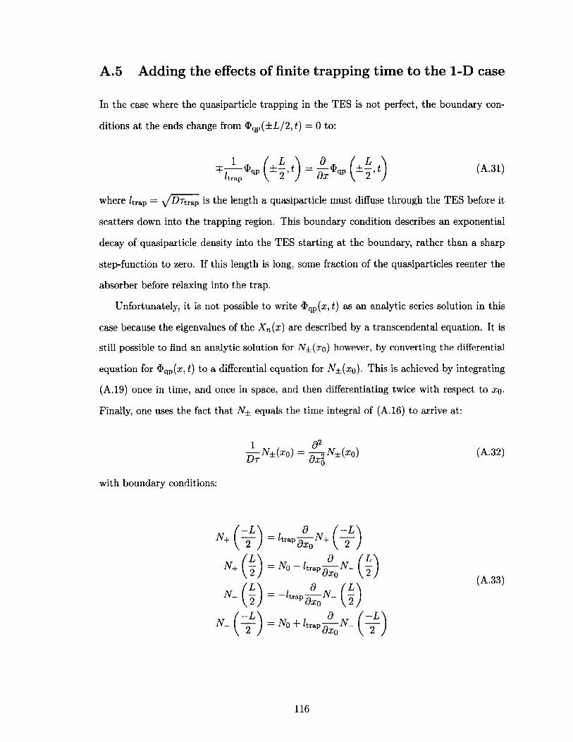
A .5 Adding the effects of finite trapping tim e to the 1-D case
In the case where the quasiparticle trapping in the TES is not perfect, the boundary con
ditions at the ends change from <Dqp(± L / 2 , t) = 0 to:
where ftrap = \ f f^Ttrap is the length a quasiparticle must diffuse through the TES before it
scatters down into the trapping region. This boundary condition describes an exponential
decay of quasiparticle density into the TES starting at the boundary, rather than a sharp
step-function to zero. If this length is long, some fraction of the quasiparticles reenter the
absorber before relaxing into the trap.
Unfortunately, it is not possible to write $ qp(x,f) as an analytic series solution in this
case because the eigenvalues of the X n(x) are described by a transcendental equation. It is
still possible to find an analytic solution for N±(xo) however, by converting the differential
equation for 3>qp(x, t) to a differential equation for N±(xo). This is achieved by integrating
(A. 19) once in time, and once in space, and then differentiating twice with respect to x q .
Finally, one uses the fact tha t N± equals the time integral of (A.16) to arrive at:
(A.31)
Dt n ±{x °) “ d 4 N±{-xo)(A.32)
with boundary conditions:
(A.33)
116
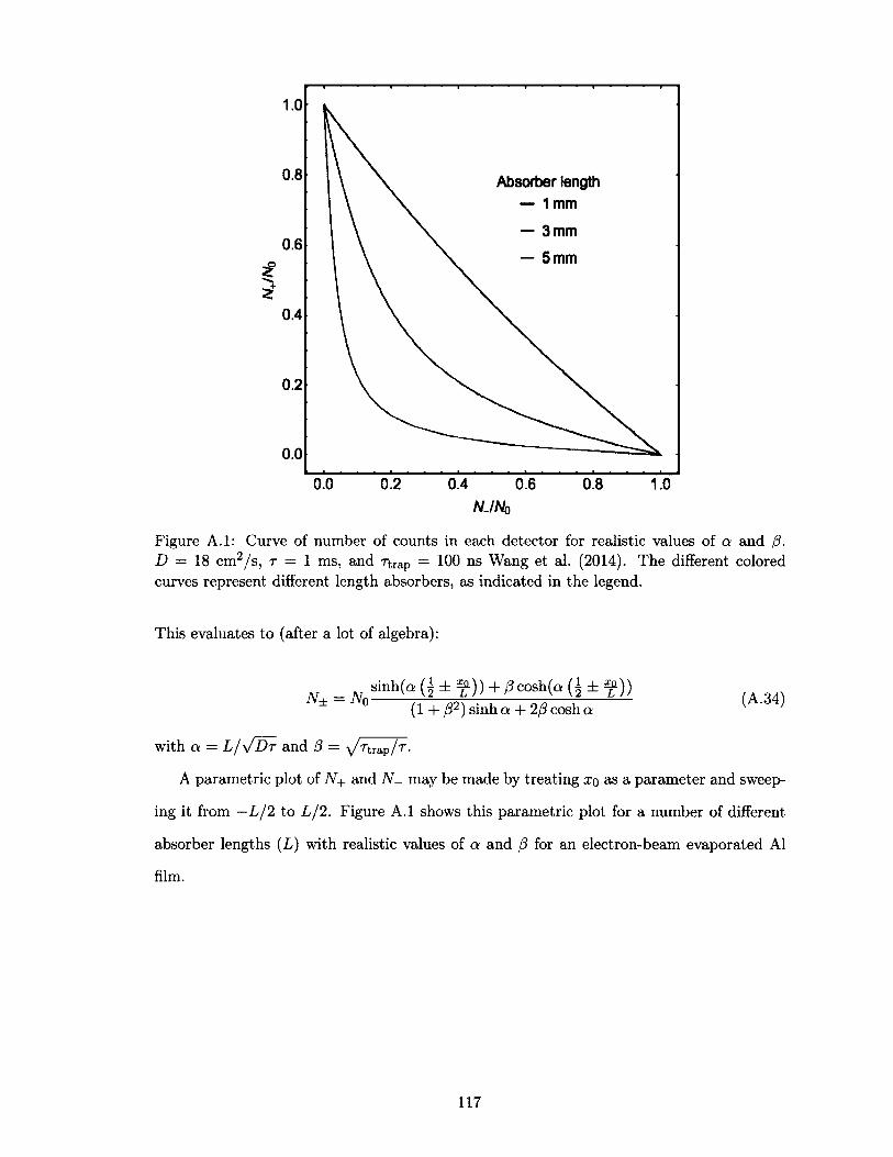
0.8 Absorber length — 1 mm
— 3 mm
— 5mm0.6
0.4
0.2
0.0
0.0 0.2 0.4 0.6 0.8 1.0NJNo
Figure A .l: Curve of number of counts in each detector for realistic values of a and j3. D — 18 cm2 /s , t — 1 ms, and r trap = 100 ns Wang et al. (2014). The different colored curves represent different length absorbers, as indicated in the legend.
This evaluates to (after a lot of algebra):
sinh(a: ± ^ ) ) + /3cosh(a (^ ± ^ ) )N ± = N0- (A.34)
(1 + /32) sinh a + 2/5 cosh a
with a = L / V D t and 0 = yVtrap/r.
A parametric plot of N+ and AT may be made by treating xo as a parameter and sweep
ing it from —L/2 to L/2. Figure A .l shows this parametric plot for a number of different
absorber lengths (L) with realistic values of a and {3 for an electron-beam evaporated Al
film.
117

Plumbing circuits nAppendix
Th e following diagrams depict the plumbing network used to fill the chamber with
helium. Every possible mode of operation is depicted, and the route the He gas
takes during each mode is highlighted in blue. Note tha t there are two inputs to the He fill
keg. One input is a thin pipe tha t extends to the back of the keg. This allows for pulling
helium from the back of the keg while replacing it at the front, thereby causing the gas in
the keg to circulate.
The first diagram depicts the electrical connectivity of the network. It was desirable to
keep as much of the plumbing network as possible electrically separated from the rest of
the experiment. This was accomplished with the use of plastic flange clamps and plastic
O-ring holders between the stainless steel bellows at certain key points. The components
sharing an electrical ground with the cryostat are highlighted in orange-red.
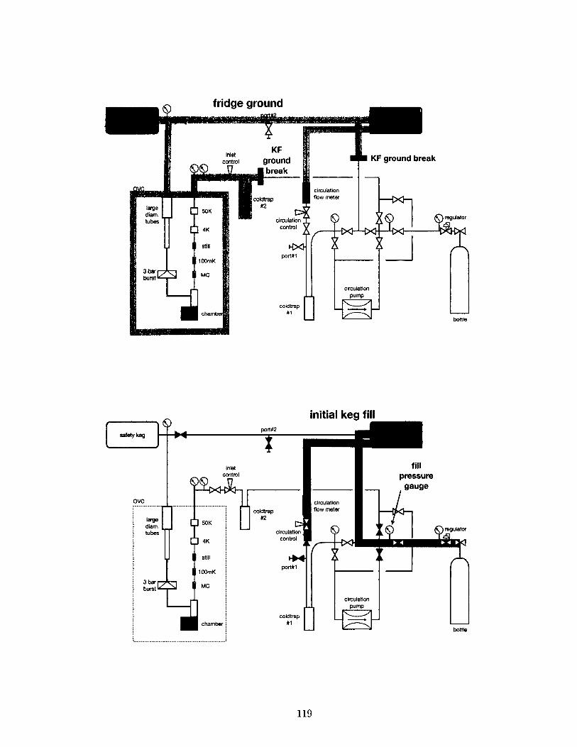
initial keg fillport#2
Hsafety keg
inletcontrol pressure
gauge
ovc circulation flow metercoldtrap
largediam.tubes
50Kregulatorcirculation
control4K
still
port#1100mK
3 bar burst MC
circulationpump
coldtrapchamber
bottle
119
circulation through cold trap
inletcontrol pump
inlet/outlet gauges
circulation flow matercoldtrap
»2
regulatorcirculationcontrol
lOOmK
3 bar burst
circulationpump
coldtrap#1chamber
bottle
condensing from storage kegsafety keg
inletcontrol
circulation flow metercoldtrap
#2largediam.tubes
regulatorcirculationcontrol
port#1100mK
3 bar burst
circulation
coldtrap#1chamber
bottle
120
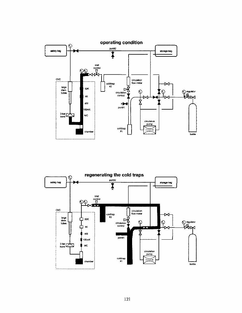
operating conditionport#2
safety Keg storage keg
inietcontrol
OVC circulation flow metercoidtrap
largediam.tubes
50Kregulatorcirculation
control4K tX -L + 4 1*}still
port#1hOOmK
3 bar burst MC
circulationpump
coldtrap
bottle
©safety keg
regenerating the cold trapsport#2I storagekeg
control
circulation flow meter
largediamtubes regulatorcirculation
control
port#t100mK
circulationpump
coldtrap#1chamber
121
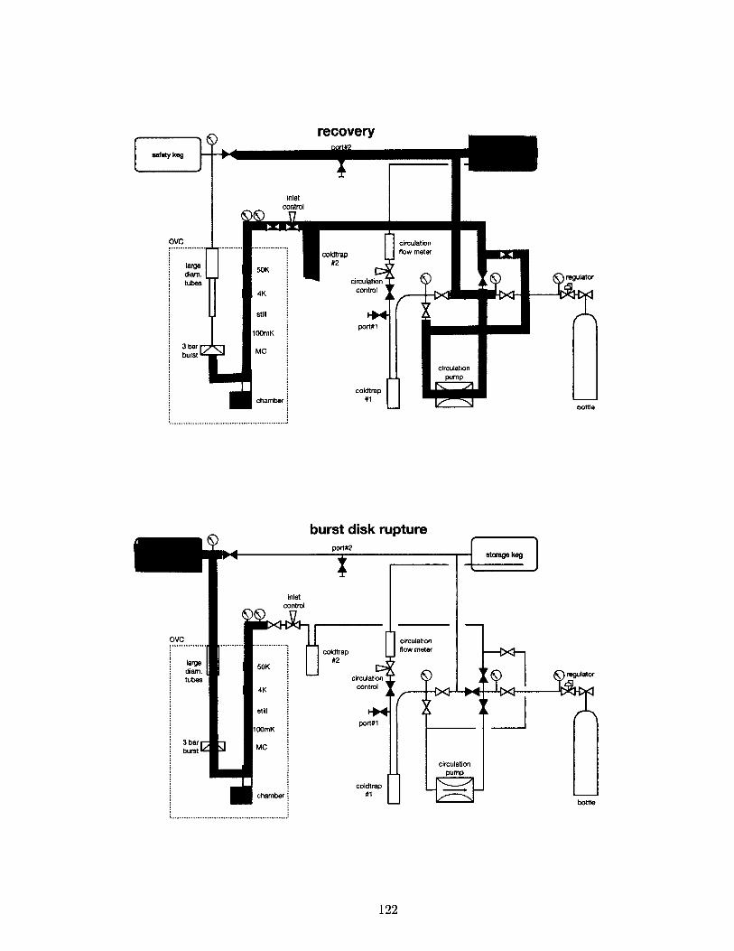
recoverysafety Keg
inletcontrol
circulation flow m etercoldtrap
#2diam.tubes
regulatorcirculation jT control ’ '
100mK
circulationpum p
coldtrapcham ber
bottle
burst disk rupture
control
circulationflow metercoldtrap
#2
(V ) regulatorcirculationcontrol
OOmK
circulation
coldtrap#1chamber
122
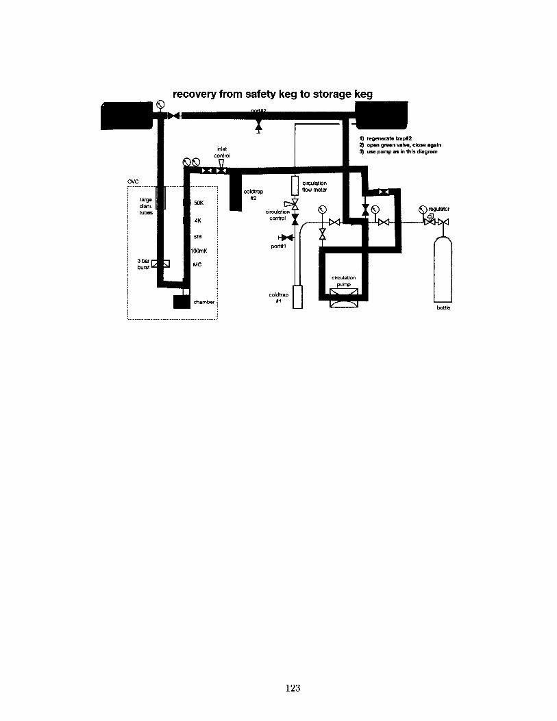
recovery from safety keg to storage keg
1) regenerate trap#22) open green valve, close again3) use pump as in this diagraminlet
control
circulation flow metercoidtrap
#2largediam.tubes
regulatorcirculationcontrol
lOOmK
circulationpum p
coldtrap#1
bottle
123

Computer codeAppendix
Ma t h e m a t i c a was chosen for solving differential equations because it has a built-
in engine tha t chooses the best method for solving a particular problem. It also
outputs very nice plots with minimal effort. D ata analysis was all handled in Igor Pro, but
tha t code is not listed here, as all the relevant algorithms are described in the text.
C .l TES differential equations
Solving the TES equations is fairly straightforward with one small exception: when the
TES switches to, or from, the super-current branch of the ib/iTES curve, it experiences a
very sharp cusp. Since the derivative of this cusp is discontinuous, the standard numerical
solver can get hung up. Luckily, the solution to the equations in the super-current region is
amenable to a simple analytic expression. This means one only needs to run the numerical
solver in the region to the right of the cusp.
The algorithm for the code is straightforward:
1. S tart at I — 0, T — 0 and run the solver until the derivative starts to change. This
location will be the cusp of the increasing current branch.
2. S tart at the end (maximum current), calculate I and T for the fully normal situation,
and work backwards until I gets close to the super-current branch.
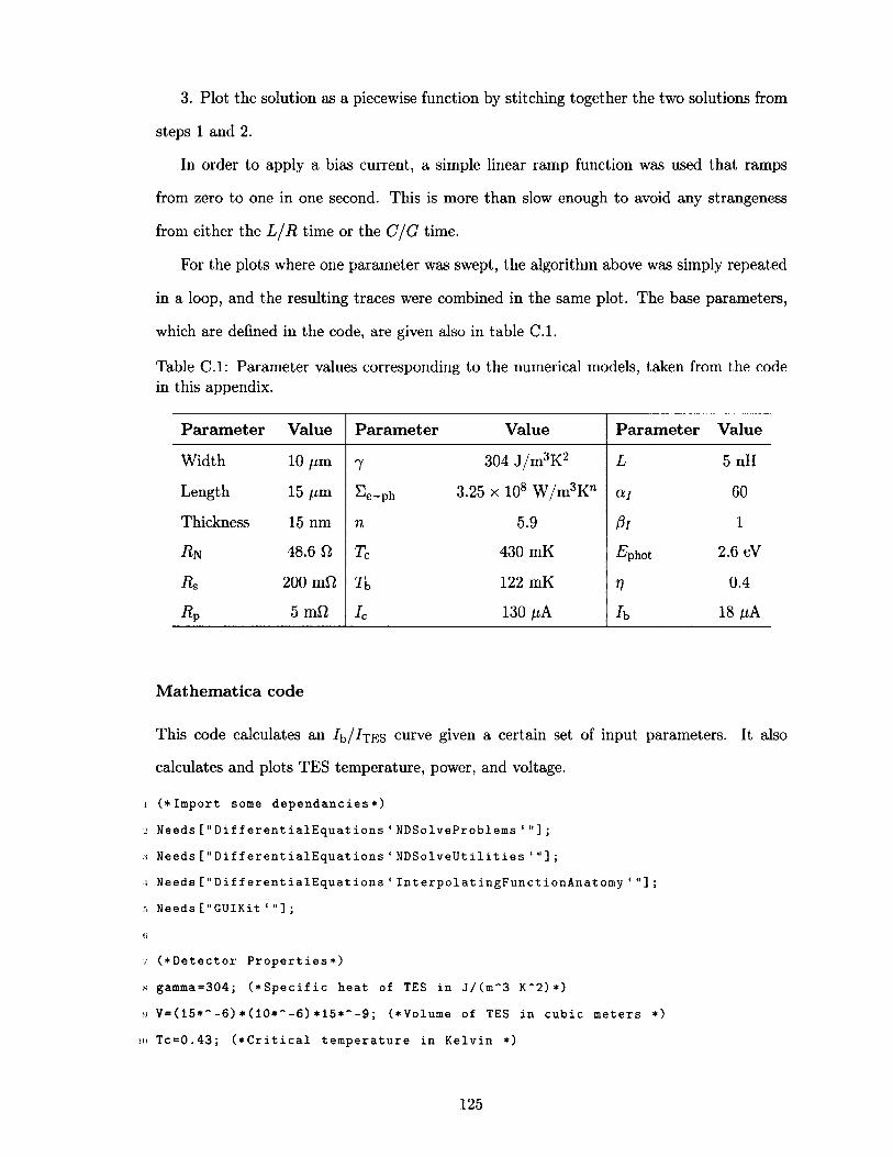
3. Plot the solution as a piecewise function by stitching together the two solutions from
steps 1 and 2 .
In order to apply a bias current, a simple linear ramp function was used tha t ramps
from zero to one in one second. This is more than slow enough to avoid any strangeness
from either the L /R time or the C/G time.
For the plots where one param eter was swept, the algorithm above was simply repeated
in a loop, and the resulting traces were combined in the same plot. The base parameters,
which are defined in the code, are given also in table C .l.
Table C .l: Parameter values corresponding to the numerical models, taken from the code in this appendix.
Parameter Value Parameter Value Parameter Value
W idth 1 0 fim 7 304 J /m 3 K 2 L 5 nH
Length 15 fim ^ e —ph 3.25 x 10⁸ W /m 3 Kn ai 60
Thickness 15 nm n 5.9 01 1
■Rn 48.6 ft Tc 430 inK Rphot 2.6 eV
Rs 2 0 0 mft Th 122 inK V 0.4
RP 5 mft Ic 130 /fA lb 18 /iA
M athem atica code
This code calculates an Ib/iTES curve given a certain set of input parameters. It also
calculates and plots TES temperature, power, and voltage.
1 ( * Im p o rt some d e p e n d e n c i e s * )
2 N e e d s [ " D i f f e r e n t i a l E q u a t i o n s ‘ N D S o l v e P r o b l e m s ‘ ;
i N e e d s [ " D i f f e r e n t i a l E q u a t i o n s ‘ N D S o l v e U t i l i t i e s ‘ " ] ;
4 N e e d s [ " D i f f e r e n t i a l E q u a t i o n s ‘I n t e r p o l a t i n g F u n c t i o n A n a t o m y ‘ ;
r, Needs ["GUIKit ‘ "] ;
7 ( * D e t e c t o r P r o p e r t i e s * )
s gamma=304; ( * S p e c i f i c h e a t o f TES i n J / ( m “3 K“2 ) * )
» V = ( 1 5 * “ - 6 ) * ( 1 0 * “ - 6 ) * 1 5 * “ - 9 ; (*Volume o f TES i n c u b i c m e t e r s *)
in T c = 0 . 4 3 ; ( * C r i t i c a l t e m p e r a t u r e i n K e l v i n *)
125
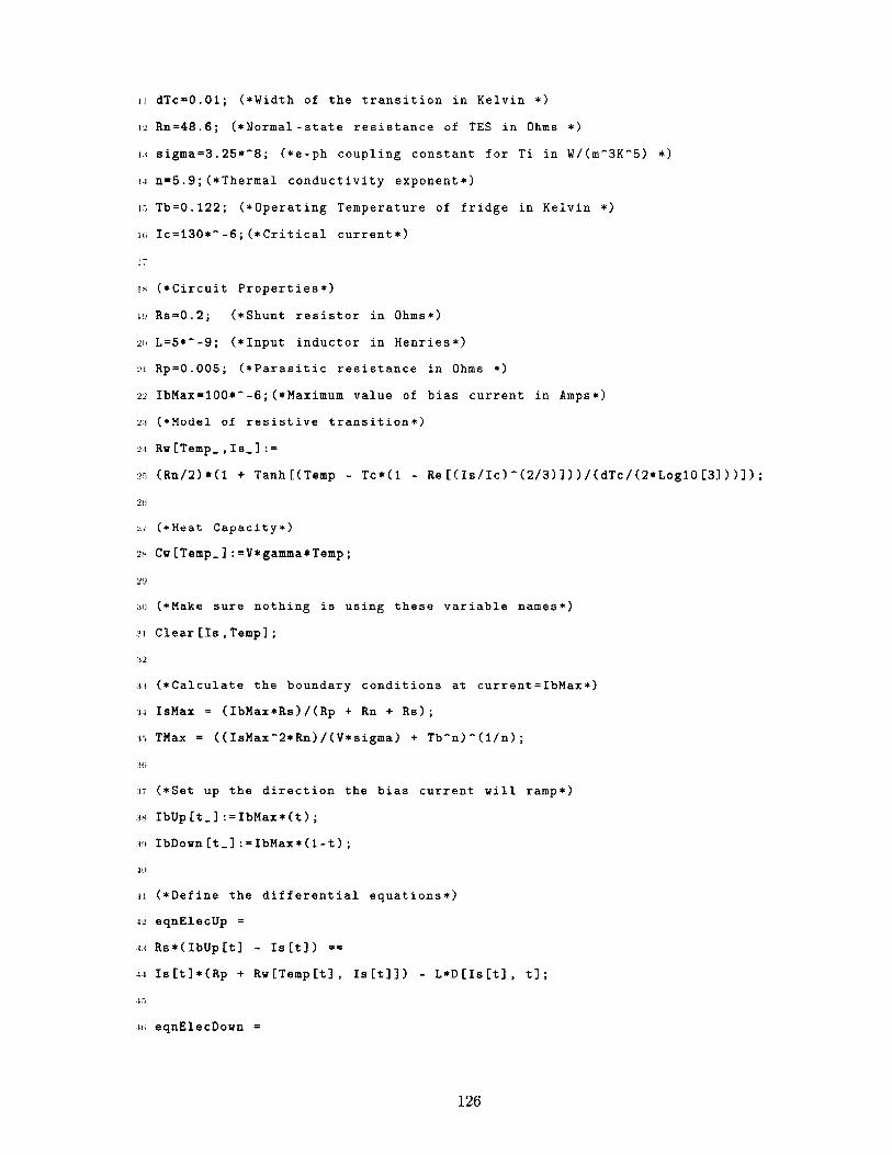
n d T c = 0 . 0 1 ; (*Width o f t h e t r a n s i t i o n in K e l v i n *)
12 R n= 4 8 .6 ; ( * N o r m a l - s t a t e r e s i s t a n c e o f TES i n Ohms *)
n s i g m a = 3 . 2 5 * “8 ; ( * e - p h c o u p l i n g c o n s t a n t f o r Ti in W/(m“3K~5) *)
ij n = 5 . 9 ; (*Thermal c o n d u c t i v i t y e x p o n e n t * )
ir, T b = 0 . 1 2 2 ; ( * O p e r a t i n g Te mp era tur e o f f r i d g e i n K e l v i n *)
io I c = i 3 0 * ~ - 6 ; ( * C r i t i c a l c u r r e n t * )
17
i* ( * C i r c u i t P r o p e r t i e s * )
io R s = 0 . 2 ; (* Sh unt r e s i s t o r i n Ohms*)
2 ii L=5*"'-9; ( * I n p u t i n d u c t o r i n H e n r i e s * )
2 i R p = 0 . 0 0 5 ; ( * P a r a s i t i c r e s i s t a n c e i n Ohms *)
2 > IbMax=1 00 *~- 6 ; (*Maximum v a l u e o f b i a s c u r r e n t in Amps*)
2 i ( *H ode l o f r e s i s t i v e t r a n s i t i o n * )
2 i Rh[Temp_, I s _ ] : =
27 ( R n / 2 ) * ( 1 + Tanh [(Temp - T c * ( l - Re [ ( I s / I c ) " ( 2 / 3 ) ] ) ) / ( d T c / (2*LoglO [ 3 ] ) ) ] ) ;
20
27 (*Hea t C a p a c i t y * )
as Cw[Temp_] : =V*gamma*Temp;
20
oo (*Make s u r e n o t h i n g i s u s i n g t h e s e v a r i a b l e names*)
31 C l e a r [ I s , Temp];
32
3) ( * C a l c u l a t e t h e boundary c o n d i t i o n s a t c u r r e n t = IbMax*)
34 IsMax = ( IbMax*Rs) / ( R p + Rn + R s ) ;
in TMax = ( ( I sM a x~ 2 *R n) / ( V * s ig m a ) + T b ~ n ) ~ ( 1 / n ) ;
30
3 7 ( * S e t up t h e d i r e c t i o n t h e b i a s c u r r e n t w i l l ramp*)
is IbUp [ t _ ] : = Ib M a x * ( t ) ;
io IbDown [ t _ ] : = IbMax* ( 1 - 1 ) ;
40
41 ( * D e f i n e t h e d i f f e r e n t i a l e q u a t i o n s * )
42 eqn ElecUp =
43 R s * ( I b U p [ t ] - I s [ t ] ) ==
it I s [ t ] * ( R p + R w [ T e m p [ t ] , I s [ t ] ] ) - L * D [ I s [ t ] , t ] ;
4.3
4o eqnElecDown =
126
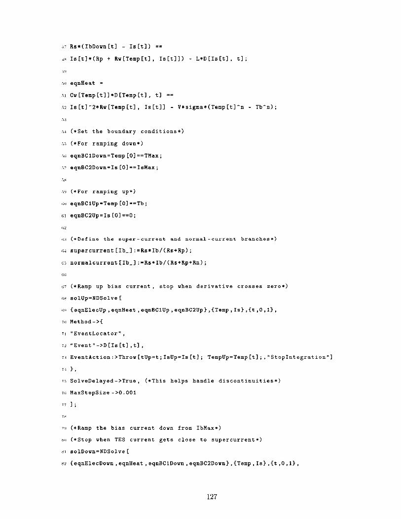
4 7 Rs * ( IbDown [ t ] - I s [ t ] ) ==
4« I s [ t ] * ( R p + R w [T e m p [ t ] , I s [ t ] ] ) - L * D [ I s [ t ] , t ] ;
■19
5 0 e q n H e a t =
si C w [ T e m p [ t ] ] *D[Temp [ t ] , t ] ==
52 I s [ t ] " 2 * R w [ T e m p [ t ] , I s [ t ] ] - V*s igma*(Temp [ t ] ~ n - T b ' n ) ;
53
51 ( * S e t t h e b o u n d a r y c o n d i t i o n s * )
5 5 ( * F o r r a m p i n g down*)
>0 eqnBClDown = Temp [0 ] ==TMax ;
5 7 eqnBC2Down = I s [ 0 ] = = IsMax ;
53
5>j ( * F o r r a m p i n g up* )
00 eqnBCiUp = Temp [ 0 ] = = T b ;
01 eqnBC2Up = I s [ 0 ]= = 0 ;
02
oo (*Define the super - current and normal - current branches*)
04 s u p e r c u r r e n t [ I b _ ] : = R s * I b / ( R s + R p ) ;
05 n o r m a l c u r r e n t [ I b _ ] : = R s * I b / ( R s + R p + R n ) ;
00
0 7 (*Ramp up b i a s c u r r e n t , s t o p when d e r i v a t i v e c r o s s e s z e r o * )
03 s o l U p = N D S o l v e [
oy { e q n E l e c U p , e q n H e a t , e q n B C l U p , eq n B C2 U p >, { T e m p , l s > , { t , 0 , l > ,
70 M e t h o d - > {
71 " E v e n t L o c a t o r " ,
72 "E v e n t " - > D [ I s [ t ] , t ] ,
73 E v e n t A c t i o n : > T h r o w [ t U p = t ; I sUp = I s [ t ] ; TempUp = T e m p [ t ] ; , " S t o p I n t e g r a t i o n "]
74 } ,
75 S o l v e D e l a y e d - > T r u e , ( * T h i s h e l p s h a n d l e d i s c o n t i n u i t i e s * )
70 M a x S t e p S i z e - > 0 . 0 0 1
77 ] ;
73
79 (*Ramp t h e b i a s c u r r e n t down f rom IbMax*)
so ( * S t o p when TES c u r r e n t g e t s c l o s e t o s u p e r c u r r e n t *)
si s o l D o w n = N D S o l v e [
82 { e q n E l e c D o w n , e q n H e a t , eqnBClDown, eqnBC2Down>, { T e m p , l s > , { t , 0 , l > ,
127
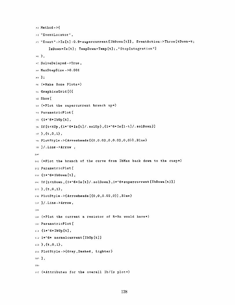
x;i Method - > {
so "E v e n t L o c a t o r ",
" E v e n t " -> I s [ t ] - 0 . 9* s u p e r c u r r e n t [ IbDown [ t ] ] , E v e n t A c t i o n : > Throw [ t D o w n = t ;
I sDown = I s [ t ] ; T e m p D o w n = T e m p [ t ] ; , " S t o p I n t e g r a t i o n "]
K<i } .
x7 S o l v e D e l a y e d - > T r u e ,
ss M a x S t e p S i z e - > 0 . 001
xi) ] ;
00 (*Make Some P l o t s * )
in G r a p h i c s G r i d [ { {
<)2 Show [
01 ( * P l o t t h e s u p e r c u r r e n t b r a n c h up* )
in P a r a m e t r i c P l o t [
in { 1 * ~ 6 * I b U p [ t ] ,
00 I f [ t < t U p , { l * ' 6 * I s [ t ] / . s o l U p } , { l * ~ 6 * I s [ l - t ] / . s o l D o w n > ]
97 } , { t , 0 , l } ,
os P l o t S t y l e - > { A r r o w h e a d s [ { 0 , 0 . 0 2 , 0 , 0 . 0 2 , 0 , 0 } ] . B l u e }
iw ] / . L i n e A r r o w ,
l Ut )
mi ( * P l o t t h e b r a n c h o f t h e c u r v e f rom IbMax b a c k down t o t h e c u s p * )
102 P a r a m e t r i c P l o t [
io.) { 1 * ~ 6 * IbDown [ t ] ,
km I f [ t < t D o w n , { 1 * " 6 * I s [ t ] / . s o l D o w n } , 1*"6* s u p e r c u r r e n t [ I b D o w n [ t ] ] ]
105 } , { t , 0 , 1 } ,
loo P l o t S t y l e - > { A r r o w h e a d s [ { 0 , 0 , 0 . 0 2 , 0 } ] . B l u e }
io7 ] / . L i n e - > Arrow ,
ID S
loo ( * P l o t t h e c u r r e n t a r e s i s t o r o f R=Rn w o u ld h a v e * )
no P a r a m e t r i c P l o t [
i n { 1 * “ 6 * I b U p [ t ] ,
112 1* ~6* n o r m a l c u r r e n t [ I b U p [ t ] ]
113 } , { t , 0 , 1 } ,
i n P l o t S t y l e - > { G r a y , D a s h e d , L i g h t e r }
115 ] ,
1 10
117 ( * A t t r i b u t e s f o r t h e o v e r a l l I b / I s p l o t * )
128
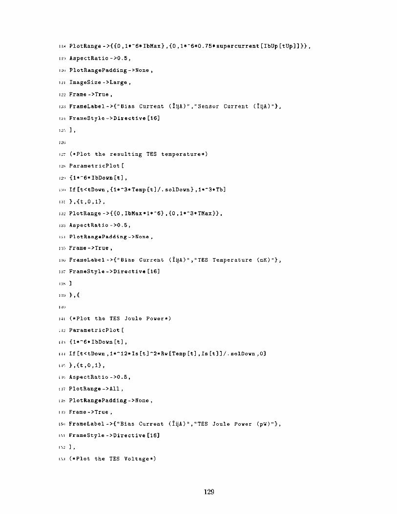
iin P l o t R a n g e - > { { 0 , 1 * “6 * I b M a x } , { 0 , 1 # ~ 6 * 0 . 7 5 * s u p e r c u r r e n t [ I b U p [ t U p ] ] } } ,
mi A s p e c t R a t i o - > 0 . 5 ,
120 P l o t R a n g e P a d d i n g - > N o n e ,
121 I m a g e S i z e - > L a r g e ,
122 F r a m e - > T r u e ,
12, i F r a m e L a b e l - > { " B i a s C u r r e n t ( I i j A ) S e n s o r C u r r e n t ( I i j A ) " } ,
i2 i F r a m e S t y l e - > D i r e c t i v e [1 6 ]
123 ] ,
120
127 ( * P l o t t h e r e s u l t i n g TES t e m p e r a t u r e * )
12* P a r a m e t r i c P l o t [
120 { 1 * ~ 6 * I b D o w n [ t ] ,
ini I f [ t < tD o w n , { l * ~ 3 * T e m p [ t ] / . s o l D o w n } , l * " 3 * T b ]
mi } , { t , 0 , l } ,
132 P l o t R a n g e - > { { 0 , I b M a x * l * ~ 6 > , { 0 , l * ~ 3 * T M a x » ,
lies A s p e c t R a t i o - >0 . 5 ,
isi P l o t R a n g e P a d d i n g - > N o n e ,
i; i3 F r a m e - > T r u e ,
iso F r a m e L a b e l - > { ”B i a s C u r r e n t ( I i j A ) " , "TES T e m p e r a t u r e (m K )" } ,
is? F r a m e S t y l e - > D i r e c t i v e [1 6 ]
I .M ]
iso } , {
I Hi
in ( * P l o t t h e TES J o u l e P o w e r * )
112 P a r a m e t r i c P l o t [
u s { 1 * ~ 6 * I b D o w n [ t ] ,
u s I f [ t < t D o w n , l * ~ 1 2 * I s [ t ] ~ 2 * R w [ T e m p [ t ] , I s [ t ] ] / . s o l D o w n , 0 ]
143 > , { t , 0 , l > ,
i4o A s p e c t R a t i o - > 0 . 5 ,
u7 P l o t R a n g e - > A 1 1 ,
i its P l o t R a n g e P a d d i n g - > N o n e ,
no F r a m e - > T r u e ,
iso F r a m e L a b e l - > { " B i a s C u r r e n t ( I i j A ) " , "TES J o u l e Power (p W ) " } ,
i.3i F r a m e S t y l e - > D i r e c t i v e [16 ]
132 ] ,
1.3:3 ( * P l o t t h e TES V o l t a g e * )
129
i5t P a r a m e t r i c P l o t [
155 - (1*~6* IbDown [ t ] ,
i5(, I f [ t < tD o w n , 1 * * 6 * I s [ t ] * R w [Temp [ t ] , I s [ t ] ] / . s o l D ow n , 0]
157 } , { t , 0 , l > ,
i.w A s p e c t R a t i o - >0 . 5 ,
i5<) P l o t R a n g e ->A11 ,
ion P l o t R a n g e P a d d i n g - > N o n e ,
ini Frame - >True ,
Ki2 F r a m e L a b e l - > { " B i a s C u r r e n t ( I i j A ) " , "TES V o l t a g e ( I i j V ) " } ,
ion F r a m e S t y l e - > D i r e c t i v e [1 6 ]
Kit ]
K15 » ]
C.2 Diffusion equation
For a discussion on the solution to the diffusion equation as it relates to TESs, see ap
pendix A.
M athem atica code
This code calculates the quasiparticle dynamics associated with a photon hit right at the
edge of the TES and the Al lead.
1 ( * S e t up some m o d e l p a r a m e t e r s * )
2 A = 1 8 0 0 ; ( * D i f f u s i o n c o n s t a n t i n m i c r o n “ 2 / s * )
:i t a u L o s s = 1 0 0 0 ; (* q u a s i p a r t i c l e l i f e t i m e i n m i c r o s e c o n d s * )
i l e n g t h = 2 0 0 ; ( * l e n g t h o f a lum inu m l e a d - - a n y t h i n g l o n g w i l l d o * )
5 s i g m a = 2; ( * d i a m e t e r o f t h e i n i t i a l q u a s i p a r t i c l e c l o u d i n m i c r o n s * )
0 I T r a p = 0 . 1 ; ( * T r a p p i n g l e n g t h i n TES i n urn*)
K
y ( * S e t up t h e d i f f u s i o n e q u a t i o n * )
io e q n D i f f = D e r i v a t i v e [ 1 , 0 ] [ u ] [ t , x ] - A * D e r i v a t i v e [ 0 , 2 ] [ u ] [ t , x ] + u [ t , x ] /
t a u L o s s == 0;
u
12 ( * S e t some b o u n d a r y c o n d i t i o n s a t e i t h e r end o f t h e a lu m in u m * )
130
is eqnBCl = D e r i v a t i v e [ 0 , 1 ] [ u ] [ t , - l e n g t h / 2 ] == ( 1 / l T r a p ) * u [ t , - l e n g t h / 2 ] ;
u eqnBC2 = D e r i v a t i v e [ 0 , 1 ] [u ] [ t , l e n g t h / 2 ] == ( - I T r a p ~ ( - 1 ) ) * u [ t , l e n g t h / 2 ] ;
i.')
io ( * S e t up t h e i n i t i a l q u a s i p a r t i c l e d i s t r i b u t i o n a s a g a u s s i a n * )
17 e q n l n i t = u [ 0 , x ] == ( 1 / ( S q r t [ 2 * P i ] * s i g m a ) ) *Exp [ - ( ( x - x O ) * 2 / ( 2 * s i g m a " 2 ) ) ] ;
18
id (*How l o n g t o run t h e s i m u l a t i o n f o r i n u s * )
2 » t e n d = 50 ;
21
22 ( * S o l v e t h e e q u a t i o n s , b u t l e a v e t h e l o c a t i o n o f t h e d i s t r i b u t i o n a s a
p a r a m e t e r * )
23 s o l = P a r a m e t r i c N D S o l v e [ { e q n D i f f , e q n B C l , e q n B C 2 , e q n l n i t } , u , { t , 0 , 1 0 } , {
x , - l e n g t h / 2 , l e n g t h / 2 } , x O ,
2 i M a x S t e p S i z e -> 0 . 1 ] ;
23
20 ( * P l o t t h e r a t e o f q u a s i p a r t i c l e s e n t e r i n g i n t o t h e TES f o r a h i t on t h e
e d g e . x 0 = 0 * )
27
28 p i t = P l o t [ {
2 d E v a l u a t e [ A * ( 1 / I T r a p ) * u [ 0 ] [ t , l e n g t h / 2 ] / . s o l ]
3t> } , { t , 0 , 1 0 } ,
31
3 2 Frame -> True ,
33 F r a m e L a b e l -> {" T im e ( l i j s ) " , " Q u a s i p a r t i c l e R a t e " } ,
34 F r a m e S t y l e -> D i r e c t i v e [18 ] ,
or, I m a g e S i z e -> La rge ,
io P l o t R a n g e -> A l l
37 ]
38
39
40 ( * C a l c u l a t e t h e t o t a l q u a s i p a r t i c l e s i n j e c t e d i n t h e TES v s t i m e * )
41 i n t = I n t e g r a t e [ { ( A / l T r a p ) * u [0 ] [ t , l e n g t h / 2 ] / . s o l } , t ] ;
42
43 p l t 2 = P l o t [
44 i n t , { t , 0 , 1 0} ,
45
131
hi Frame -> True ,
47 F r a m e L a b e l -> {" Tim e ( I i j s ) " , " Q u a s i p a r t i c l e s a b s o r b e d i n TES1' } ,
is F r a m e S t y l e -> D i r e c t i v e [18 ] ,
io I m a g e S i z e -> La rg e ,
so P l o t R a n g e -> A l l
51 ]
132
Fabrication I 1 recipes J_-/
Appendix
ALL of the fabrication was done at Yale University. Electron-beam lithography was
accomplished with the Raith EBPG 5000+ at the Yale Institute for Nanoscience
and Quantum Engineering. Wet processing and metal deposition was done at the Yale
Clean Room.
D .l Wafer cleaning
The wafer is sonicated for 2 minutes each in N-methyl-2-pyrrolidone (NMP), acetone, and
methanol, and then blow-dried with dry nitrogen.
D.2 Single layer resist
The wafer is spun with a 4% solution of 950k polymethyl methacrylate (PMMA) in anisole
(A4) at 2500 rpm for 60 s. It is then baked on a hotplate for 5 min at 180° C. This results
in a layer of PMMA tha t is about 200 nm thick.
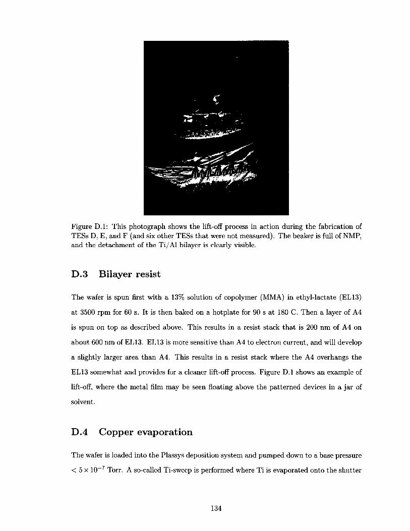
Figure D .l: This photograph shows the lift-off process in action during the fabrication of TESs D, E, and F (and six other TESs tha t were not measured). The beaker is full of NMP, and the detachment of the T i/A l bilayer is clearly visible.
D.3 Bilayer resist
The wafer is spun first with a 13% solution of copolymer (MMA) in ethyl-lactate (EL13)
at 3500 rpm for 60 s. It is then baked on a hotplate for 90 s at 180 C. Then a layer of A4
is spun on top as described above. This results in a resist stack tha t is 200 nm of A4 on
about 600 nm of EL13. EL13 is more sensitive than A4 to electron current, and will develop
a slightly larger area than A4. This results in a resist stack where the A4 overhangs the
EL13 somewhat and provides for a cleaner lift-off process. Figure D .l shows an example of
lift-off, where the metal film may be seen floating above the patterned devices in a ja r of
solvent.
D.4 Copper evaporation
The wafer is loaded into the Plassys deposition system and pumped down to a base pressure
< 5 x 10- 7 Torr. A so-called Ti-sweep is performed where Ti is evaporated onto the shutter
134
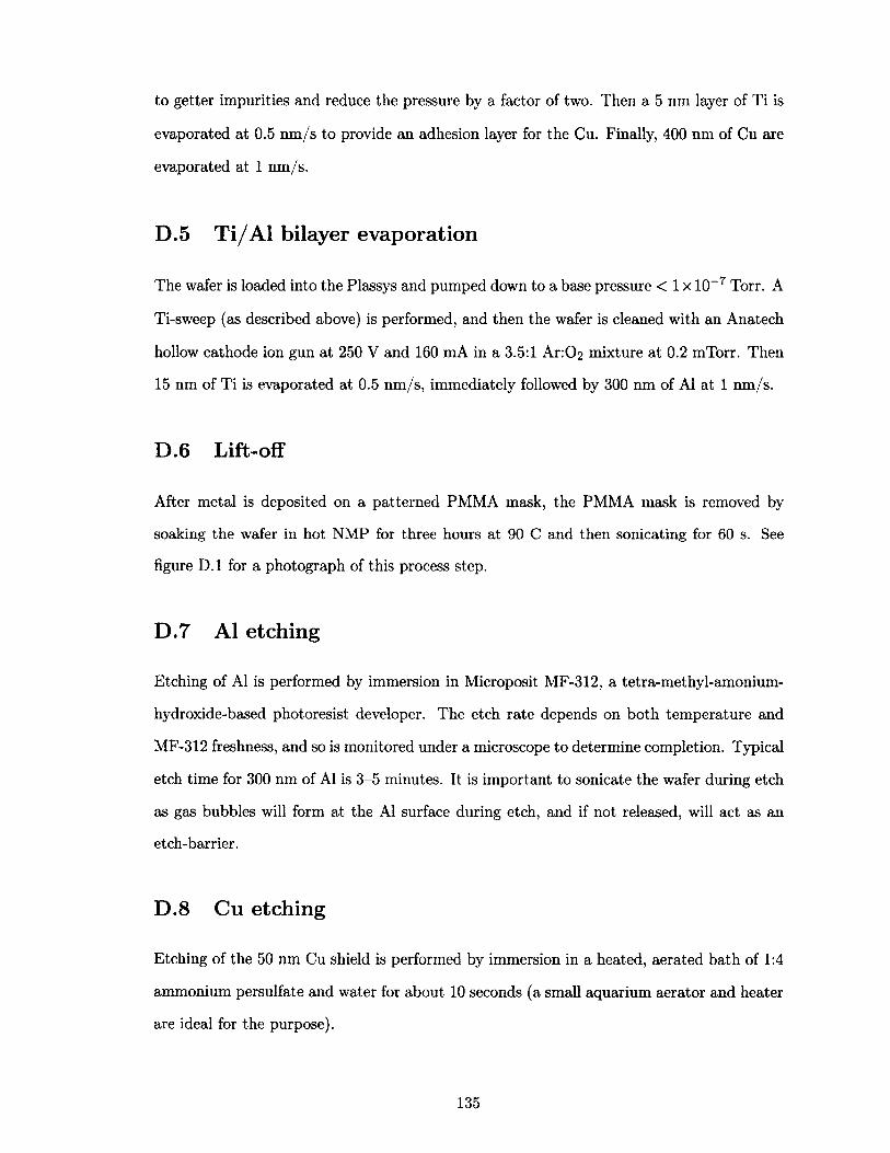
to getter impurities and reduce the pressure by a factor of two. Then a 5 nm layer of Ti is
evaporated at 0.5 nm /s to provide an adhesion layer for the Cu. Finally, 400 nm of Cu are
evaporated at 1 nm/s.
D.5 T i/A l bilayer evaporation
The wafer is loaded into the Plassys and pumped down to a base pressure < 1 x 10- 7 Torr. A
Ti-sweep (as described above) is performed, and then the wafer is cleaned with an Anatech
hollow cathode ion gun at 250 V and 160 mA in a 3.5:1 A r : 0 2 mixture at 0.2 mTorr. Then
15 nm of Ti is evaporated at 0.5 nm /s, immediately followed by 300 nm of A1 at 1 nm /s.
D.6 Lift-off
After metal is deposited on a patterned PMMA mask, the PMMA mask is removed by
soaking the wafer in hot NMP for three hours at 90 C and then sonicating for 60 s. See
figure D .l for a photograph of this process step.
D .7 A1 etching
Etching of A1 is performed by immersion in Microposit MF-312, a tetra-methyl-amonium-
hydroxide-based photoresist developer. The etch rate depends on both tem perature and
MF-312 freshness, and so is monitored under a microscope to determine completion. Typical
etch time for 300 nm of A1 is 3-5 minutes. It is im portant to sonicate the wafer during etch
as gas bubbles will form at the A1 surface during etch, and if not released, will act as an
etch-barrier.
D .8 Cu etching
Etching of the 50 nm Cu shield is performed by immersion in a heated, aerated bath of 1:4
ammonium persulfate and water for about 1 0 seconds (a small aquarium aerator and heater
are ideal for the purpose).
135

D .9 Electron beam lithography: writing and developing
D.9.1 Beam current and dose
All e-beam lithography is performed on a Raith EBPG 5000+. It is a 100 keV system
capable of providing beam currents of several hundred nA. For the resists described above,
spun on a Si substrate, a beam current of 50-150 nA is used for an electric charge dose of
700 /iC/'cm2. The fact tha t pattern centers naturally receive a higher dose than pattern
edges is nullified through an automatic routine tha t estimates the actual dose at each point
in the pattern required to achieve an effective dose of 700 fiC/cm2.
D .9.2 Developing E-beam resist
After writing, the wafer is developed by immersion in a 3:1 isopropanohwater solution kept
at 7 C. The wafer is immersed for 2 min. The wafer is sonicated for the last 30 s of
development.
136

Sources of noise I—Iand interference -I—/
Appendix
Id e a l l y , the experiment would be housed in a perfect Faraday cage to prevent electromag
netic (EM) interference, installed in a basement on a concrete slab connected directly
to bedrock to prevent vibrations, and connected to a magical set of noise-free instruments
and computers powered by clean linear power supplies. In this experimental utopia, the
nearest other scientist is miles away in her own perfect Faraday cage, and the measurement
noise floor is limited only by the intrinsic noise of the TES detectors. This is an unlikely
scenario. The experiment discussed in this dissertation shared a room with three qubit-
based experiments, each with a large collection of RF generators, synchronization clocks,
computer controllers, and resourceful graduate students who use narrow bandpass filters
to pretend they live in a clean EM environment. Furthermore, the building the experi
ment is in has an interesting (euphemism for maddening) electrical wiring configuration
tha t somehow manages to couple building utilities and experiments together in a variety
of unintelligible ways tha t introduce interference covering the spectrum from a few mHz to
a few kHz. The computers used all contain highly-efficient switched mode power supplies
tha t broadcast loudly in and around the AM radio band, and the SQUID amplifiers used to
read out the TES are so sensitive to current tha t rolling a large ungrounded helium dewar
across the floor can induce a measurable current spike. Interference can be dealt with in
one of four ways: Remove the source; filter out the source; fix the ground-loop tha t picks
up the source; or ignore the source. The following short sections discuss how these methods
were applied to the majority of interference sources encountered in this work. An excellent
reference for mitigating noise and interference issues is O tt (2009), which was consulted
heavily throughout the operation of this work.
E .l Computers (and other electronics)
By far the noisiest piece of equipment in the lab is the common switch-mode computer
power supply. This supply switches on and off at hundreds of kHz and is a modern marvel
of efficiency. It is also very loud! The ~100 kHz signal it creates is broadcast out into the
room by anything resembling an antenna, most often by the power cord tha t plugs into
the wall and by any USB cables. The best way to deal with this solution is to buy an
old linear power supply or make a battery supply and use tha t for the computer. These
can be hard to find however, and annoying to mate to modern motherboard connectors.
A good alternative is to get a large ferrite toroid and wrap the power supply cord around
it as many times as possible. The toroid should be as close to the end of the cord that
plugs into the computer as possible. Smaller toroids may be used for USB cables in the
same manner. This effectively puts a large inductor in series with the antenna/power cord
and attenuates the noisy signal. If possible, the computer should also be plugged into a
completely separate electrical panel than the one used for the oscilloscope or other readout
instruments. Otherwise, the circuit ground in the wall can inject the noisy power-supply
signal right back into the readout. Figure E .l shows an example of how to set this up.
Another good option is to use a battery-powered laptop computer as the measurement
computer. Laptops are, from an unwanted noise perspective, very quiet!
Switch-mode power supplies are found in nearly every piece of modern electronics, so i t’s
possible tha t more than just the computer may interfere with an experiment. In addition
to the computer, the network switches and routers in the lab were also found to emit a fair
bit of unwanted signal. Happily, Ethernet cables can be quite long and still function well,
so the solution here is to just move the offending piece of electronics far away.
The static DC power supplies tha t were integrated into the high-voltage setup were also
138
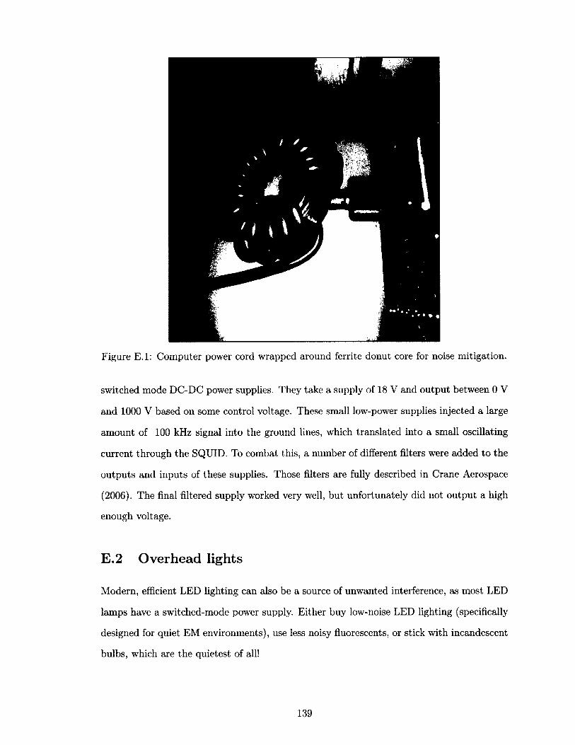
Figure E .l: Computer power cord wrapped around ferrite donut core for noise mitigation.
switched mode DC-DC power supplies. They take a supply of 18 V and output between 0 V
and 1000 V based on some control voltage. These small low-power supplies injected a large
amount of 100 kHz signal into the ground lines, which translated into a small oscillating
current through the SQUID. To combat this, a number of different filters were added to the
outputs and inputs of these supplies. Those filters are fully described in Crane Aerospace
(2006). The final filtered supply worked very well, but unfortunately did not output a high
enough voltage.
E.2 Overhead lights
Modern, efficient LED lighting can also be a source of unwanted interference, as most LED
lamps have a switched-mode power supply. Either buy low-noise LED lighting (specifically
designed for quiet EM environments), use less noisy fluorescents, or stick with incandescent
bulbs, which are the quietest of all!
139
E.3 Vibrations
The mechanical resonant frequency of the dilution refrigerator is between 9-10 Hz. Any
vibration source (from the pulse-tube cryocooler to the building’s HVAC system) is enough
to excite this resonance. In practice, this interference source manifested as a small square-
wave type signal every 100 ms or so tha t contains frequency components as high as 300 Hz.
A 1 kHz high-pass filter takes care of this problem from an electrical standpoint, but to
really solve the problem (and keep the cryostat tem perature from responding to vibrations)
vibrational isolators should be installed on the cryostat.
140

Bibliography
R. G. K. M. Aarts and A. T. A. M. de Waele, “Numerical investigation of the flow
properties of He II,” Phys. Rev. B 50 (14), pages 10069-10079 (1994).
doi: 10.1103/PhysRevB.50.10069.
J. Adams, Energy deposition by electrons in superfluid helium, Ph.D. thesis, Brown
University (2001).
D. H. Andrews, W. F. Brucksch, W. T. Ziegler, and E. R. Blanchard, “Attenuated
superconductors: I. For measuring infra-red radiation,” Rev. Sci. Instrum. 13 (7), pages
281-292 (1942). doi: 10.1063/1.1770037.
R. Baptist and G. Chauvet, “Inverse photoemission of platinum,” J. Phys. C Solid State
Phys. 15 (10), pages 2313-2320 (2000). doi:10.1088/0022-3719/15/10/030.
J. Bardeen, L. N. Cooper, and J. R. Schrieffer, “Theory of superconductivity,” Phys. Rev.
108 (5), pages 1175-1204 (1957). doi:10.U03/PhysRev.l08.1175.
A. V. Benderskii, R. Zadoyan, N. Schwentner, and V. A. Apkarian, “Photodynamics in
superfluid helium: Femtosecond laser-induced ionization, charge recombination, and
preparation of molecular Rydberg states,” J. Chem. Phys. 110 (3), pages 1542-1557
(1999). doi: 10.1063/1.477796.
M. J. Berger, J. H. Hubbell, S. M. Seltzer, J. Chang, J. S. Coursey, R. Sukumar, and D. S.
Zucker, “XCOM: photon cross sections database,” NIST Stand. Ref. Database 8 , pages
87-3597 (1998).
G. P. Bewley, D. P. Lathrop, and K. R. Sreenivasan, “Superfluid helium: visualization of
quantized vortices.” Nature 441 (7093), page 588 (2006). doi:10.1038/441588a.
G. P. Bewley, K. R. Sreenivasan, and D. P. Lathrop, “Particles for tracing turbulent liquid
helium,” Exp. Fluids 44 (6 ), pages 887-896 (2008). doi:10.1007/s00348-007-0444-6.
A. I. Bezuglyi and V. A. Shklovskii, “The kinetics of low-temperature electron-phonon
relaxation in a metallic film following instantaneous heating of the electrons,” J. Exp.
Theor. Phys. 84 (6 ), pages 1149-1163 (1997). doi:10.1134/1.558253.
D. F. Bogorin, Superconducting Iridium Thin Films as Transition Edge Sensors, Ph.D.
thesis, University of Miami (2008).
D. F. Bogorin and M. Galeazzi, “Characterization of iridium thin films for TES
microcalorimeters,” J. Low Temp. Phys. 151 (1-2), pages 167-172 (2008).
doi: 10.1007/sl0909-007-9622-4.
P. L. Brink, Non-equilibrium superconductivity induced by x-ray photons, Ph.D. thesis,
Oxford University (1995).
J. S. Butterworth, C. R. Brome, P. R. Huffman, C. E. H. Mattoni, D. N. McKinsey, and
J. M. Doyle, “A demountable cryogenic feedthrough for plastic optical fibers,” Rev. Sci.
Instrum. 69 (10), pages 3697-3698 (1998). doi:10.1063/l.1149161.
F. W. Carter, S. A. Hertel, M. J. Rooks, D. N. McKinsey, and D. E. Prober, “Toward the
In Situ Detection of Individual He^ Excimers Using a Ti TES in Superfluid Helium,”
IEEE Trans. Appl. Supercond. 25 (3), pages 1-7 (2014).
doi: 10.1109/TASC.2014.2372673.
Crane Aerospace, “Measurement and Filtering of Output Noise of DC / DC Converters,”
(2006). URL h t tp :
/ / m m . in te r p o in t . com/product_documents/DC_DC_Converters_Output_Noise.pdf.
J. P. Delaboudiniere, G. E. Artzner, J. Brunaud, A. H. Gabriel, J. F. Hochedez, F. Millier,
X. Y. Song, B. Au, K. P. Dere, R. A. Howard, R. Kreplin, D. J. Michels, J. D. Moses,
142
J. M. Defise, C. Jam ar, P. Rochus, J. P. Chauvineau, J. P. Marioge, R. C. Catura, J. R.
Lemen, L. Shing, R. A. Stern, J. B. Gurman, W. M. Neupert, A. Maucherat, F. Clette,
P. Cugnon, and E. L. Van Dessel, “EIT: Extreme-ultraviolet Imaging Telescope for the
SOHO mission,” Sol. Phys. 162 (1-2), pages 291-312 (1995). doi:10.1007/BF00733432.
D. Eastman, “Photoemission energy level measurements of sorbed gases on titanium ,”
Solid State Commun. 10 (10), pages 933-935 (1972). doi:10.1016/0038-1098(72)90225-6.
A. A. Fragner, Circuit Quantum Electrodynamics with Electrons on Helium, Ph.D. thesis,
Yale University (2013).
D. Fukuda, “TES x-ray microcalorimeters with single element superconductors,” AIP
Conf. Proc. 605 (1 ), pages 263-266 (2002). doi:10.1063/1.1457643.
M. E. Gershenson, D. Gong, T. Sato, B. S. Karasik, and A. V. Sergeev, “Millisecond
electron-phonon relaxation in ultrathin disordered metal films at millikelvin
tem peratures,” Appl. Phys. Lett. 79 (13), pages 2049—2051 (2001).
doi:10.1063/l. 1407302.
A. I. Golov and H. Ishimoto, “Sharp and stable metal tips for helium ionization at mK
temperatures,” J. low Temp. Phys. 113, pages 957-962 (1998).
doi: 10.1023/A: 1022583729253.
W. Guo, M. La Mantia, D. P. Lathrop, and S. W. Van Sciver, “Visualization of two-fluid
flows of superfluid helium-4,” Proc. Natl. Acad. Sci. I l l (Supplement_1), pages
4653-4658 (2014). doi:10.1073/pnas.l312546111.
W. Guo and D. N. McKinsey, “Concept for a dark m atter detector using liquid helium-4,”
Phys. Rev. D - Part. Fields, Gravit. Cosmol. 87 (11), page 115001 (2013).
doi: 10.1103/PhysRevD.87.115001.
W. Guo, J. D. Wright, S. B. Cahn, J. A. Nikkei, and D. N. McKinsey, “Metastable helium
molecules as tracers in superfluid He4,” Phys. Rev. Lett. 102 (23), pages 4-7 (2009).
doi:10.1103/PhysRevLett. 102.235301.
143
A. L. Hagstrom, A. Platau, and S.-E. Kaelsson, “Adsorption of oxygen at room
temperature on polycrystalline titanium studied by ultraviolet and X-ray photoelectron
spectroscopy,” Phys. Status Solidi 83 (1 ), pages 77-84 (1977).
doi: 10.1002/pssb.2220830107.
D. M. Hanson, R. Stockbauer, and T. E. Madey, “Photon-stimulated desorption and other
spectroscopic studies of the interaction of oxygen with a titanium (001) surface,” Phys.
Rev. B 24 (10), pages 5513-5521 (1981). doi:10.1103/PhysRevB.24.5513.
Y. Harada, S. Masuda, and H. Ozaki, “Electron Spectroscopy Using Metastable Atoms as
Probes for Solid Surfaces.” Chem. Rev. 97 (6 ), pages 1897-1952 (1997).
doi: 10.1021/cr940315v.
R. V. Hogg, J. McKean, and A. T. Craig, Introduction to Mathematical Statistics,
Pearson, 7 edition (1972), ISBN 0321795431.
K. D. Irwin, “An application of electrothermal feedback for high resolution cryogenic
particle detection,” Appl. Phys. Lett. 6 6 (15), page 1998 (1995). doi:10.1063/1.113674.
K. D. Irwin and G. C. Hilton, “Transition-edge sensors,” Top. Appl. Phys. 99, pages
63-152 (2005). doi:10.1007/10933596_3.
T. M. Ito and G. M. Seidel, “Scintillation of liquid helium for low-energy nuclear recoils,”
Phys. Rev. C - Nucl. Phys. 8 8 (2), pages 1-13 (2013). doi:10.1103/PhysRevC.88.025805.
P. B. Johnson and R. W. Christy, “Optical constants of transition metals: Ti, V, Cr, Mn,
Fe, Co, Ni, and Pd,” Phys. Rev. B 9 (12), pages 5056-5070 (1974).
doi:10.1103/PhysRevB.9.5056.
B. S. Karasik, S. V. Pereverzev, A. Soibel, D. F. Santavicca, D. E. Prober, D. Olaya, and
M. E. Gershenson, “Energy-resolved detection of single infrared photons with A = 8 pm
using a superconducting microbolometer,” Appl. Phys. Lett. 101 (5), page 052601
(2012). doi: 10.1063/1.4739839.
J. W. Keto, F. J. Soley, M. Stockton, and W. A. Fitzsimmons, “Dynamic properties of
neutral excitations produced in electron-bombarded superfluid helium. I. The He(2 S3)
144
and He2(a 3) atomic and molecular metastable states,” Phys. Rev. A 10 (3), pages
872-886 (1974). doi: 10.1103/PhysRevA. 10.872.
J. W. Keto, M. Stockton, and W. A. Fitzsimmons, “Dynamics of atomic and molecular
metastable states produced in electron-bombarded superfluid helium,” Phys. Rev. Lett.
28 (13), pages 792-795 (1972). doi:10.1103/PhysRevLett.28.792.
K. Kinnunen, Studies of transition-edge sensor physics: thermal models and noise, Ph.D.
thesis, University of Jyvaskyla (2011).
W. F. Krolikowski and W. E. Spicer, “Photoemission Studies of the Noble Metals. II.
Gold,” Phys. Rev. B 1 (2), pages 478-487 (1970). doi:10.1103/PhysRevB.1.478.
M. La Mantia, T. V. Chagovets, M. Rotter, and L. Skrbek, “Testing the performance of a
cryogenic visualization system on thermal counterflow by using hydrogen and deuterium
solid tracers,” (2012), doi: 10.1063/1.4719917.
S. P. Langley, “The Bolometer and Radiant Energy,” Proc. Am. Acad. Arts Sci. 16, pages
342-358 (1880). doi:10.2307/25138616.
L. Li, X-ray single photon imaging detectors using superconducting tunnel junctions, Ph.D.
thesis, Yale University (2003).
M. A. Lindeman, K. A. Barger, D. E. Brandi, S. G. Crowder, L. Rocks, and
D. McCammon, “Accurate thermal conductance and impedance measurements of
transition edge sensors,” J. Low Temp. Phys. 151 (1-2), pages 180-184 (2008).
doi:10.1007/sl0909-007-9616-2.
A. E. Lita, B. Calkins, L. A. Pellochoud, A. J. Miller, and S. W. Nam, “High-effieieney
photon-number-resolving detectors based on hafnium transition-edge sensors,” in AIP
Conf. Proc., volume 1185, ISBN 9780735407510 (2009) pages 351-354,
doi: 10.1063/1.3292350.
A. E. Lita, D. Rosenberg, S. W. Nam, A. J. Miller, D. Balzar, L. M. Kaatz, and R. E.
Schwall, “Tuning of tungsten thin film superconducting transition tem perature for
145
fabrication of photon number resolving detectors,” IEEE Trans. Appl. Supercond. 15 (2
PART III), pages 3528-3531 (2005). doi:10.1109/TASC.2005.849033.
M. Loidl, S. Cooper, O. Meier, F. Probst, G. Safran, W. Seidel, M. Sisti, L. Stodolsky, and
S. Uchaikin, “Quasiparticle diffusion over several mm in cryogenic detectors,” Nucl.
Instruments Methods Phys. Res. Sect. A Accel. Spectrometers, Detect. Assoc. Equip.
465 (2-3), pages 440-446 (2001). doi:10.1016/S0168-9002(01)00621-0.
J. C. Mather, “Bolometer noise: nonequilibrium theory.” Appl. Opt. 2 1 (6 ), pages
1125-1129 (1982). doi:10.1364/A0.21.001125.
J. C. Mather, E. S. Cheng, D. A. Cottingham, J. Eplee, R. E., D. J. Fixsen,
T. Hewagama, R. B. Isaacman, K. A. Jensen, S. S. Meyer, P. D. Noerdlinger, S. M.
Read, L. P. Rosen, R. A. Shafer, E. L. Wright, C. L. Bennett, N. W. Boggess, M. G.
Hauser, T. Kelsall, J. Moseley, S. H., R. F. Silverberg, G. F. Smoot, R. Weiss, and D. T.
W ilkinson, “Measurement of the cosmic microwave background spectrum by the COBE
FIRAS instrum ent,” Astrophys. J. 420, page 439 (1994). doi: 10.1086/173574.
P. V. E. McClintock, D. J. Meredith, and J. K. Wigmore, Matter at Low Temperatures,
Blackie Academic & Professional (1984), ISBN 9780216915947.
D. N. McKinsey, C. R. Brome, J. S. Butterworth, S. Dzhosyuk, P. R. Huffman,
C. M attoni, J. M. Doyle, R. Golub, and K. Habicht, “Radiative decay of the metastable
He2 (a3 E+) molecule in liquid helium,” Phys. Rev. A 59 (1), pages 200-204 (1999).
doi:10.1103/PhysRevA.59.200.
D. N. McKinsey, W. H. Lippincott, J. A. Nikkei, and W. G. Rellergert, “Trace detection of
metastable helium molecules in superfluid helium by laser-induced fluorescence,” Phys.
Rev. Lett. 95 (11), page 111101 (2005). doi:10.1103/PhysRevLett.95.111101.
H. W. O tt, Electromagnetic Compatibility Engineering, Wiley (2009), ISBN
9780470189306, doi: 10.1002/9780470508510.
M. S. Paoletti, M. E. Fisher, K. R. Sreenivasan, and D. P. Lathrop, “Velocity statistics
146
distinguish quantum turbulence from classical turbulence,” Phys. Rev. Lett. 101 (15)
(2008). doi:10.1103/PhysRevLett. 101.154501.
F. Pobell, Matter and Methods at Low Temperatures, Springer Berlin Heidelberg, Berlin,
Heidelberg (2007), ISBN 3540463569, doi:10.1007/978-3-540-46360-3_l.
C. Portesi, E. Taralli, L. Lolli, M. Rajteri, and E. Monticone, “Fabrication and
Characterization of Fast TESs W ith Small Area for Single Photon Counting,” IEEE
Trans. Appl. Supercond. 25 (3), pages 1-4 (2015). doi:10.1109/TASC.2014.2367455.
W. H. Press, S. A. Teukolsky, W. T. Vetterling, and B. P. Flannery, Numerical Recipes:
The Art of Scientific Computing (3rd edition), Cambridge University Press (2007),
ISBN 9780521880688.
W. G. Rellergert, S. B. Cahn, A. Garvan, J. C. Hanson, W. H. Lippincott, J. A. Nikkei,
and D. N. McKinsey, “Detection and imaging of He2 molecules in superfluid helium,”
Phys. Rev. Lett. 100 (2), pages 1-4 (2008). doi:10.1103/PhysRevLett.100.025301.
D. F. Santavicca, B. Reulet, B. S. Karasik, S. V. Pereverzev, D. Olaya, M. E. Gershenson,
L. Frunzio, and D. E. Prober, “Characterization of terahertz single-photon-sensitive
bolometric detectors using a pulsed microwave technique,” in AIP Conf. Proc., volume
1185, ISBN 9780735407510 (2009) pages 72-75, doi:10.1063/1.3292445.
D. F. Santavicca, B. Reulet, B. S. Karasik, S. V. Pereverzev, D. Olaya, M. E. Gershenson,
L. Frunzio, and D. E. Prober, “Energy resolution of terahertz single-photon-sensitive
bolometric detectors,” Appl. Phys. Lett. 96 (8 ), page 083505 (2010).
doi: 10.1063/1.3336008.
S. Sato, K. Okazaki, and S. Ohno, “The Estimation of the G-Values for the Ionization and
Excitation of Noble Gases Irradiated by 100 keV Electrons,” Bull. Chem. Soc. Jpn.
47 (9), pages 2174-2180 (1974). doi:10.1246/bcsj.47.2174.
A. V. Sergeev and V. V. Mitin, “Electron-phonon interaction in disordered conductors:
Static and vibrating scattering potentials,” Phys. Rev. B 61 (9), pages 6041-6047
(2000). doi:10.1103/PhysRevB.61.6041.
147
Y. A. Sergeev and C. F. Barenghi, “Particles-Vortex Interactions and Flow Visualization
in 4He,” J. Low Temp. Phys. 157 (5-6), pages 429-475 (2009).
doi: 10.1007/ sl0909-009-9994-8.
M. J. Shaw, “Penning ionization,” Contemp. Phys. 15 (5), pages 445-464 (1974).
doi:10.1080/00107517408210804.
M. Shen, Low Temperature Electron-Phonon Interaction in Disordered Metal Thin Films
and Applications to F ast, Sensitive Sub-Millimeter Photon Sources and Detectors,
Ph.D. thesis, Yale University (2005).
N. V. Smith, “Photoelectron energy spectra and the band structures of the noble metals,”
Phys. Rev. B 3 (6), pages 1862-1878 (1971). doi:10.1103/PhysRevB.3.1862.
M. Stockton, J. W. Keto, and W. A. Fitzsimmons, “Ultraviolet Emission Spectrum of
Electron-Bombarded Superfluid Helium,” Phys. Rev. Lett. 24 (12), pages 654-657
(1970). doi:10.1103/PhysRevLett.24.654.
E. Taralli, C. Portesi, L. Lolli, E. Monticone, M. Rajteri, I. Novikov, and J. Beyer,
“Impedance measurements on a fast transition-edge sensor for optical and near-infrared
range,” Supercond. Sci. Technol. 23 (10), page 105012 (2010).
doi: 10.1088/0953-2048/23/10/105012.
D. W. Tokaryk, R. L. Brooks, and J. L. Hunt, “Reaction dynamics of metastable helium
molecules and atoms near 4.2 K,” Phys. Rev. A 48 (1), pages 364-381 (1993).
doi: 10.1103/PhysRevA.48.364.
M. I. Trioni, G. Butti, N. Bonini, and G. P. Brivio, “Metastable helium spectroscopy on
simple metals: Comparison between low and high work function substrates,” Surf. Sci.
587 (1-2), pages 121-127 (2005). doi:10.1016/j.susc.2005.04.040.
G. Ventura, M. Barucci, E. Pasca, E. Monticone, and M. Rajteri, “Development of Ti
Based Transition Edge Sensors for Cryogenic Detectors,” in Adv. Technol. Part. Phys.,
World Scientific Publishing Co. Pte. Ltd., Singapore, ISBN 9789812381804 (2002) pages
677-683, doi:10.1142/9789812776464_0096.
148
R. Wagner, P. J. Ras, P. Remeijer, S. C. Steel, and G. Frossati, “Observation of 3He
crystallization down to 1 mK using a cooled CCD camera,” J. Low Temp. Phys.
95 (5-6), pages 715-728 (1994). doi:10.1007/BF00754712.
C. Wang, Y. Y. Gao, I. M. Pop, U. Vool, C. Axline, T. Brecht, R. W. Heeres, L. Frunzio,
M. H. Devoret, G. Catelani, L. I. Glazman, and R. J. Schoelkopf, “Measurement and
Control of Quasiparticle Dynamics in a Superconducting Qubit,” Nat. Commun. 5,
page 7 (2014). doi:10.1038/ncomms6836.
T. S. Wang, G. C. Guo, Q. F. Zhu, J. X. Wang, T. F. Li, J. S. Liu, W. Chen, and X. Zhou,
“Device modeling of superconductor transition-edge sensors based on the two-fluid
theory,” IEEE Trans. Appl. Supercond. 22 (4) (2012). doi:10.1109/TASC.2012.2196041.
J. Wei, D. Olaya, B. S. Karasik, S. V. Pereverzev, A. V. Sergeev, and M. E. Gershenson,
“Ultrasensitive hot-electron nanobolometers for terahertz astrophysics.” Nat.
Nanotechnol. 3 (8), pages 496-500 (2008). doi:10.1038/nnano.2008.173.
C. M. Wilson, L. Frunzio, and D. E. Prober, “Superconducting tunnel junction detectors
for extreme ultraviolet applications,” IEEE Trans. Appl. Supercond. 13 (2 I), pages
1120-1123 (2003). doi:10.1109/TASC.2003.814170.
D. L. W indt, W. C. Cash, M. Scott, P. Arendt, B. Newnam, R. F. Fisher, and A. B.
Swartzlander, “Optical constants for thin films of Ti, Zr, Nb, Mo, Ru, Rh, Pd, Ag, Hf,
Ta, W, Re, Ir, Os, P t, and Au from 24 A to 1216 A.” Appl. Opt. 27 (2), pages 246-278
(1988). doi: 10.1364/A0.27.000246.
T. Zhang, D. Celik, and S. W. Van Sciver, “Tracer Particles for Application to PIV
Studies of Liquid Helium,” J. Low Temp. Phys. 134 (3/4), pages 985-1000 (2004).
doi:10.1023/B:JOLT.0000013213.61721.51.
T. Zhang and S. W. Van Sciver, “Large-scale turbulent flow around a cylinder in
counterflow superfluid 4He (He (II)),” Nat. Phys. 1 (1), pages 36-38 (2005).
doi:10.1038/nphysll4.
149
D. E. Zmeev, F. Pakpour, P. M. Walmsley, A. I. Golov, W. Guo, D. N. McKinsey, G. G.
Ihas, P. V. E. McClintock, S. N. Fisher, and W. F. Vinen, “Excimers He2* as tracers of
quantum turbulence in He4 in the T = 0 Limit,” Phys. Rev. Lett. 110 (17), page 175303
(2013a). doi:10.1103/PhysRevLett. 110.175303.
D. E. Zmeev, F. Pakpour, P. M. Walmsley, A. I. Golov, P. V. E. McClintock, S. N. Fisher,
W. Guo, D. N. McKinsey, G. G. Ihas, and W. F. Vinen, “Observation of crossover from
ballistic to diffusion regime for excimer molecules in superfluid 4He,” J. Low Temp.
Phys. 171 (3-4), pages 207-213 (2013b). doi:10.1007/sl0909-012-0720-6.
150


![arXiv:2010.15488v1 [quant-ph] 29 Oct 2020cas.ensmp.fr/~leghtas/papers/Smith_2020.pdf · 2020. 11. 5. · plemented with Josephson junction arrays and C is de-termined by the speci](https://img.dokumen.tips/doc/110x75/60b64c448e02c057614ab1d4/arxiv201015488v1-quant-ph-29-oct-leghtaspaperssmith2020pdf-2020-11-5.jpg)


![arXiv:1711.01208v2 [quant-ph] 25 Apr 2018 · Dynamics of a qubit while simultaneously monitoring its relaxation and dephasing Q. Ficheux,1,2 S. Jezouin,2 Z. Leghtas,3,2,4 and B. Huard1,2,](https://img.dokumen.tips/doc/110x75/5e0b744d903b2079035d4144/arxiv171101208v2-quant-ph-25-apr-2018-dynamics-of-a-qubit-while-simultaneously.jpg)