Embed Size (px)
Citation preview
1
A Successful Industry
Collaboration Model to Achieve
Toxics Use Reduction
Greg Morose
Toxics Use Reduction Institute
University of Massachusetts Lowell
November 4, 2009
2
Lead in Electronics
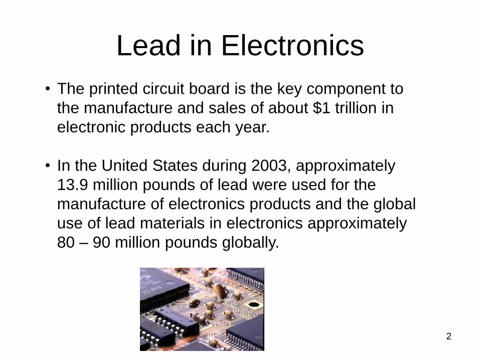
• The printed circuit board is the key component to
the manufacture and sales of about $1 trillion in
electronic products each year.
• In the United States during 2003, approximately
13.9 million pounds of lead were used for the
manufacture of electronics products and the global
use of lead materials in electronics approximately
80 – 90 million pounds globally.
3
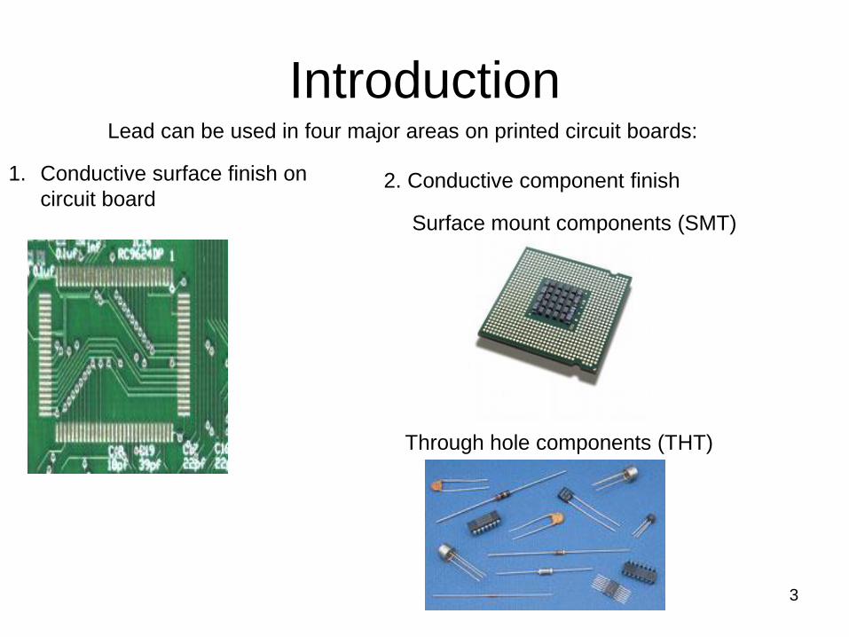
Introduction Lead can be used in four major areas on printed circuit boards:
1. Conductive surface finish on
circuit board
2. Conductive component finish
Surface mount components (SMT)
Through hole components (THT)

4
Introduction 3. Bar solder for assembly of through-hole components
4. Solder paste for the assembly of surface mount components
5
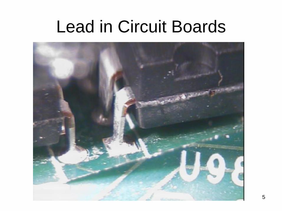
Lead in Circuit Boards

6
Human Health Effects
Acute effects of lead exposure:
Chronic effects of lead exposure:
Brain damage, kidney damage, and gastrointestinal distress
occur from acute exposure to high levels of lead in humans. The
most sensitive targets for the acute toxic effects of lead are the
kidneys and the hematological, cardiovascular, and nervous
systems.
EPA considers lead to be a Group B2, probable human
carcinogen. Chronic exposure to lead in humans can affect the
blood, reproductive, and the nervous system.
7
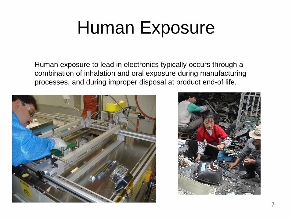
Human Exposure
Human exposure to lead in electronics typically occurs through a
combination of inhalation and oral exposure during manufacturing
processes, and during improper disposal at product end-of life.
8
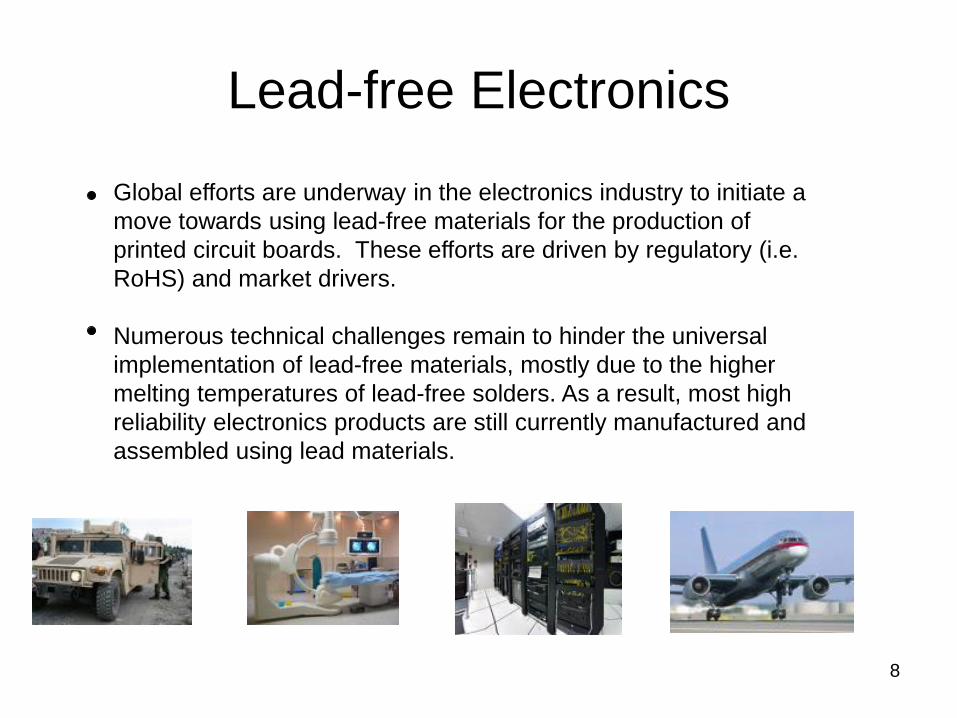
Lead-free Electronics
Global efforts are underway in the electronics industry to initiate a
move towards using lead-free materials for the production of
printed circuit boards. These efforts are driven by regulatory (i.e.
RoHS) and market drivers.
Numerous technical challenges remain to hinder the universal
implementation of lead-free materials, mostly due to the higher
melting temperatures of lead-free solders. As a result, most high
reliability electronics products are still currently manufactured and
assembled using lead materials.
9
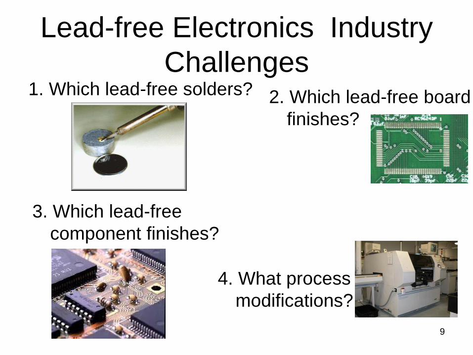
Lead-free Electronics Industry
Challenges
4. What process
modifications?
2. Which lead-free board
finishes?
3. Which lead-free
component finishes?
1. Which lead-free solders?
10
Lead-free Electronics Initiatives
• Company specific initiatives
• Industry association sponsored initiatives
• Government/academia/industry partnerships
11
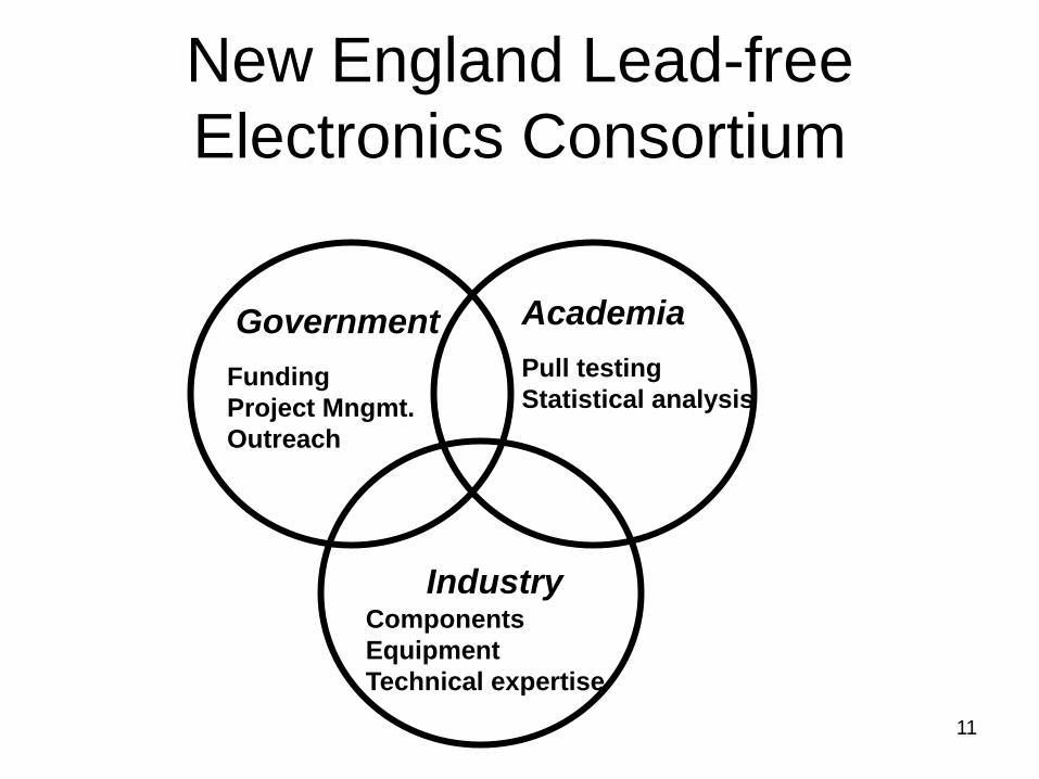
New England Lead-free
Electronics Consortium
Government Academia
Industry
Pull testing
Statistical analysis Funding
Project Mngmt.
Outreach
Components
Equipment
Technical expertise

12
Consortium Plan
Objectives:
Design, assemble, and test printed circuit boards using lead-free materials
to achieve equal or better solder joint integrity for lead-free electronics
assembly as compared to leaded electronics assembly.
Share and disseminate the research results with consortium members as
well as the entire electronics industry.

13
Consortium Members Project Manager:
Greg Morose, TURI
General Consortium Members
Subgroups: Assigned to address specific tasks
• FMEA creation subgroup
• Design subgroup
• Rework subgroup
• Reliability subgroup
Representatives from industry, government, and academia
14
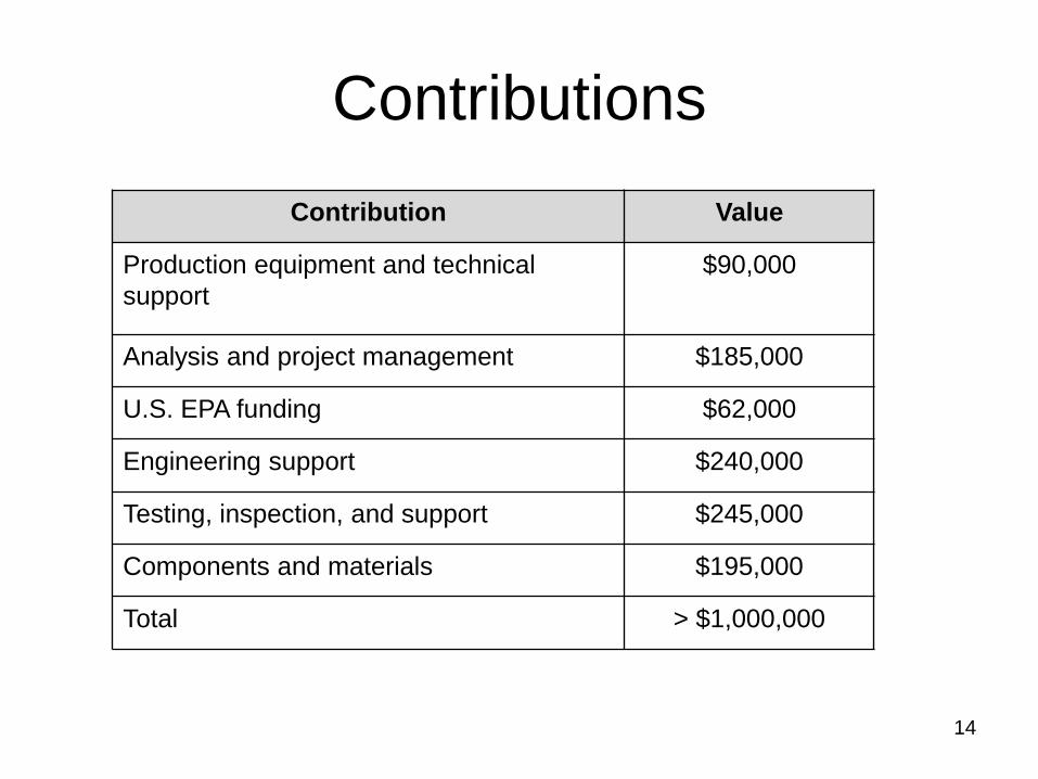
Contributions
Contribution Value
Production equipment and technical
support
$90,000
Analysis and project management $185,000
U.S. EPA funding $62,000
Engineering support $240,000
Testing, inspection, and support $245,000
Components and materials $195,000
Total > $1,000,000
15
Phase IV Contributors

16
Consortium Communication • Bimonthly consortium meetings
• Subgroup meetings (design, rework, reliability)
• Distribution of meeting materials and meeting minutes
• Subgroup documentation and presentation of results
• Surveys
• Workshops and conferences
• Develop papers and articles for submission to electronics
publications and electronics conferences
• Presentation at major electronics conferences
• Maintain consortium website
17
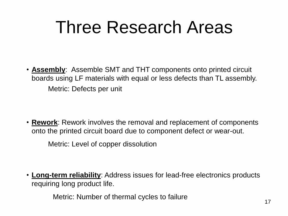
Three Research Areas
• Assembly: Assemble SMT and THT components onto printed circuit
boards using LF materials with equal or less defects than TL assembly.
• Rework: Rework involves the removal and replacement of components
onto the printed circuit board due to component defect or wear-out.
• Long-term reliability: Address issues for lead-free electronics products
requiring long product life.
Metric: Defects per unit
Metric: Level of copper dissolution
Metric: Number of thermal cycles to failure

18
Six Sigma Approach - DMAIC
Measure Analyze Improve Control
Initiate the
Project
Define the
Process
Determine
Customer
Requirements
Define Key
Process
Output
Variables
Verify Critical
Inputs Using
Planned
Experiments
Design
Improvement
Pilot New
Process
(Implement)
Analyze Data
to Prioritize
Key Input
Variables
Identify Waste
Finalize the
Control
System
Verify Long
Term
Capability
Understand
the Process
Evaluate Risks
on Process
Inputs
Develop and
Evaluate
Measurement
Systems
Measure
Current
Process
Performance
Define
19
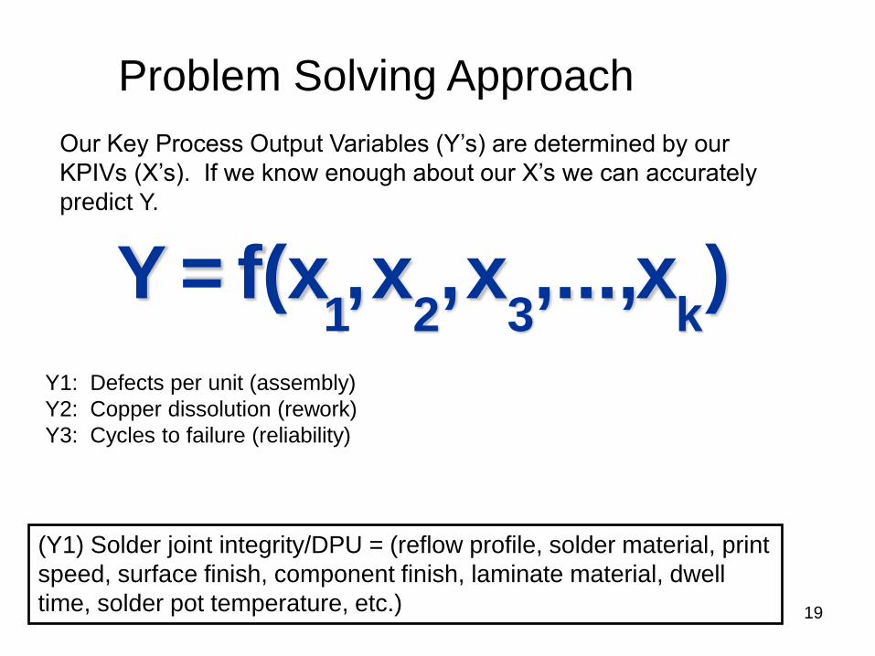
Our Key Process Output Variables (Y’s) are determined by our
KPIVs (X’s). If we know enough about our X’s we can accurately
predict Y.
Y1: Defects per unit (assembly)
Y2: Copper dissolution (rework)
Y3: Cycles to failure (reliability)
(Y1) Solder joint integrity/DPU = (reflow profile, solder material, print
speed, surface finish, component finish, laminate material, dwell
time, solder pot temperature, etc.)
) x ,..., x , x , f(x = Y k 3 2 1
Problem Solving Approach
20
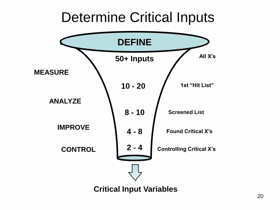
Critical Input Variables
50+ Inputs
8 - 10
4 - 8
DEFINE
2 - 4
Found Critical X’s
Controlling Critical X’s
10 - 20
All X’s
1st “Hit List”
Screened List
ANALYZE
IMPROVE
CONTROL
MEASURE
Determine Critical Inputs
21
Methods Used to Reduce X’s
• Phase I, II, and III experiment results
• Surveys and meetings with technical experts
• Cause and Effect diagrams
• Failure Modes and Effects Analysis (FMEA)
22
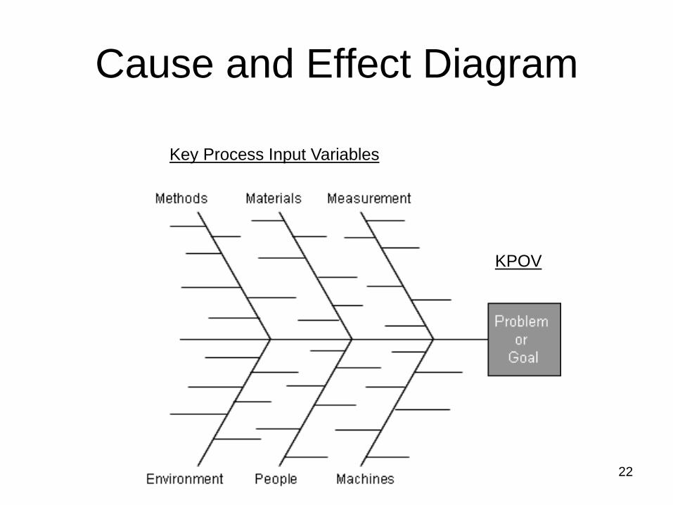
Cause and Effect Diagram
Key Process Input Variables
KPOV
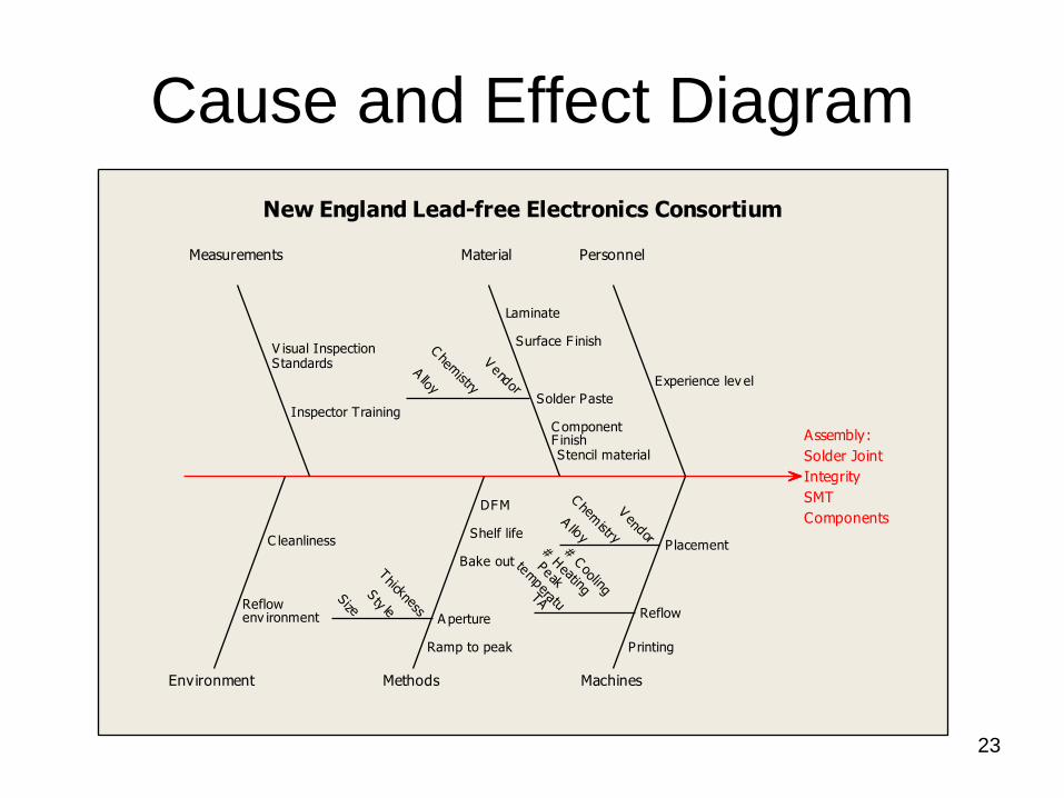
23
Cause and Effect Diagram
Components
SMT
Integrity
Solder Joint
Assembly:
Environment
Measurements
Methods
Material
Machines
Personnel
Experience lev el
P lacement
Reflow
Printing
Stencil materialF inishC omponent
Solder Paste
Surface F inish
Laminate
DFM
Shelf life
Bake out
A perture
Ramp to peak
Inspector Training
StandardsV isual Inspection
C leanliness
env ironmentReflow
# C
ooling
# H
eating
temperatu
PeakTA
Vendor
Chem
istry
Alloy
Vendor
Chem
istry
Alloy
Thickness
Sty le
Size
New England Lead-free Electronics Consortium
24
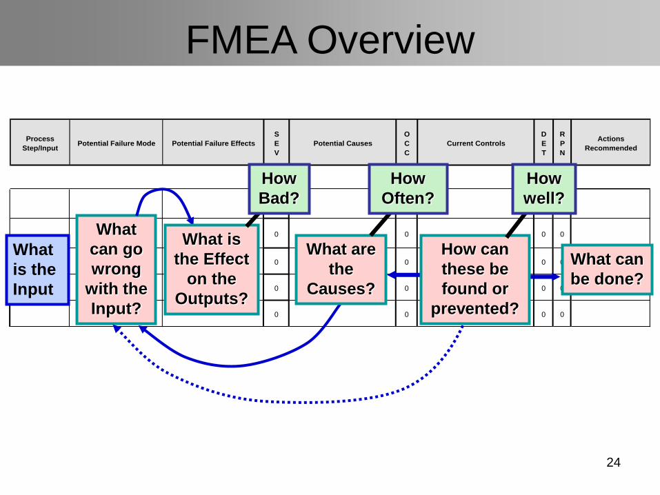
FMEA Overview
Process
Step/InputPotential Failure Mode Potential Failure Effects
S
E
V
Potential Causes
O
C
C
Current Controls
D
E
T
R
P
N
Actions
Recommended
0 0 0 0
0 0 0 0
0 0 0 0
0 0 0 0
0 0 0 0
What
is the
Input
What
can go
wrong
with the
Input?
What can
be done?
What is
the Effect
on the
Outputs?
What are
the
Causes?
How can
these be
found or
prevented?
How
Bad?
How
Often?
How
well?
Effects Causes Controls
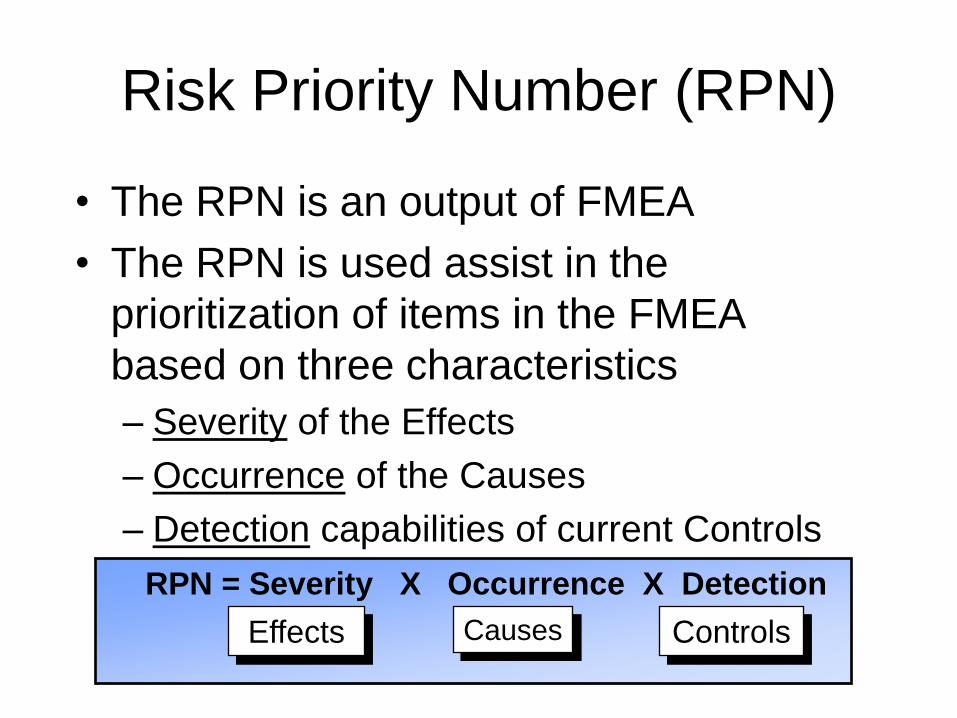
RPN = Severity X Occurrence X Detection
Risk Priority Number (RPN)
• The RPN is an output of FMEA
• The RPN is used assist in the
prioritization of items in the FMEA
based on three characteristics
– Severity of the Effects
– Occurrence of the Causes
– Detection capabilities of current Controls
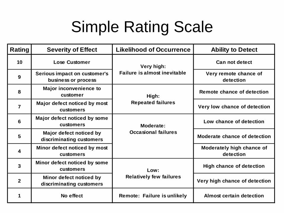
Simple Rating Scale
Rating Severity of Effect Likelihood of Occurrence Ability to Detect
10 Lose CustomerVery high:
Can not detect
9Serious impact on customer's
business or process
Failure is almost inevitable Very remote chance of
detection
8Major inconvenience to
customer High:Remote chance of detection
7Major defect noticed by most
customers
Repeated failuresVery low chance of detection
6Major defect noticed by some
customers Moderate:Low chance of detection
5Major defect noticed by
discriminating customers
Occasional failuresModerate chance of detection
4Minor defect noticed by most
customers
Moderately high chance of
detection
3Minor defect noticed by some
customers Low:High chance of detection
2Minor defect noticed by
discriminating customers
Relatively few failuresVery high chance of detection
1 No effect Remote: Failure is unlikely Almost certain detection

27
FMEA Page 1 of 5
28
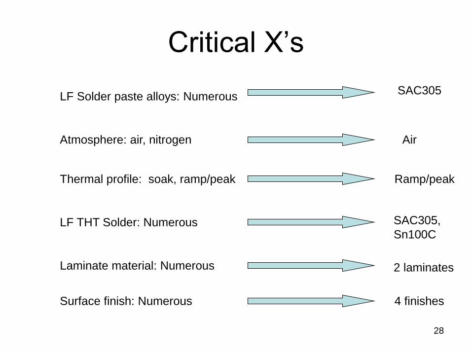
Critical X’s
LF Solder paste alloys: Numerous
Atmosphere: air, nitrogen
LF THT Solder: Numerous
Thermal profile: soak, ramp/peak
Laminate material: Numerous
Surface finish: Numerous
SAC305
Air
Ramp/peak
SAC305,
Sn100C
2 laminates
4 finishes
29
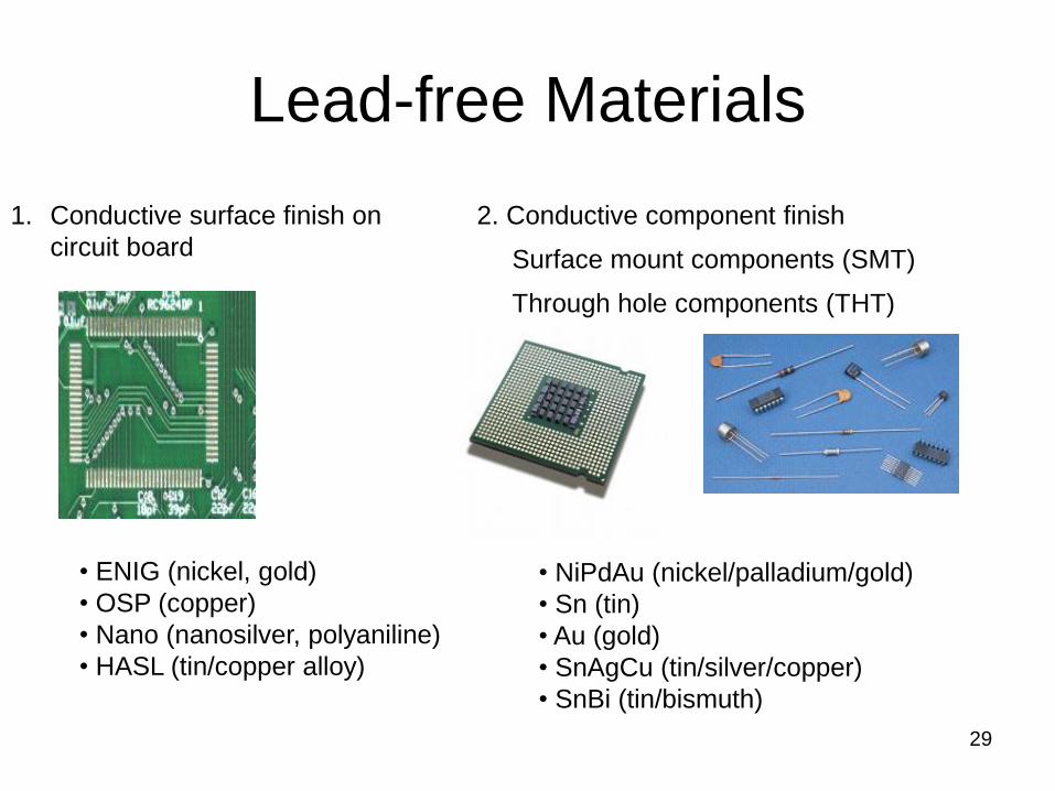
Lead-free Materials
1. Conductive surface finish on
circuit board
2. Conductive component finish
Surface mount components (SMT)
Through hole components (THT)
• ENIG (nickel, gold)
• OSP (copper)
• Nano (nanosilver, polyaniline)
• HASL (tin/copper alloy)
• NiPdAu (nickel/palladium/gold)
• Sn (tin)
• Au (gold)
• SnAgCu (tin/silver/copper)
• SnBi (tin/bismuth)

30
Lead-free Materials 3. Bar solder for assembly
of through-hole components 4. Solder paste for the assembly
of surface mount components
• Tin/copper (Sn100C)
• Tin/silver/copper (SAC305)
• Tin/silver/copper (SAC305)
31
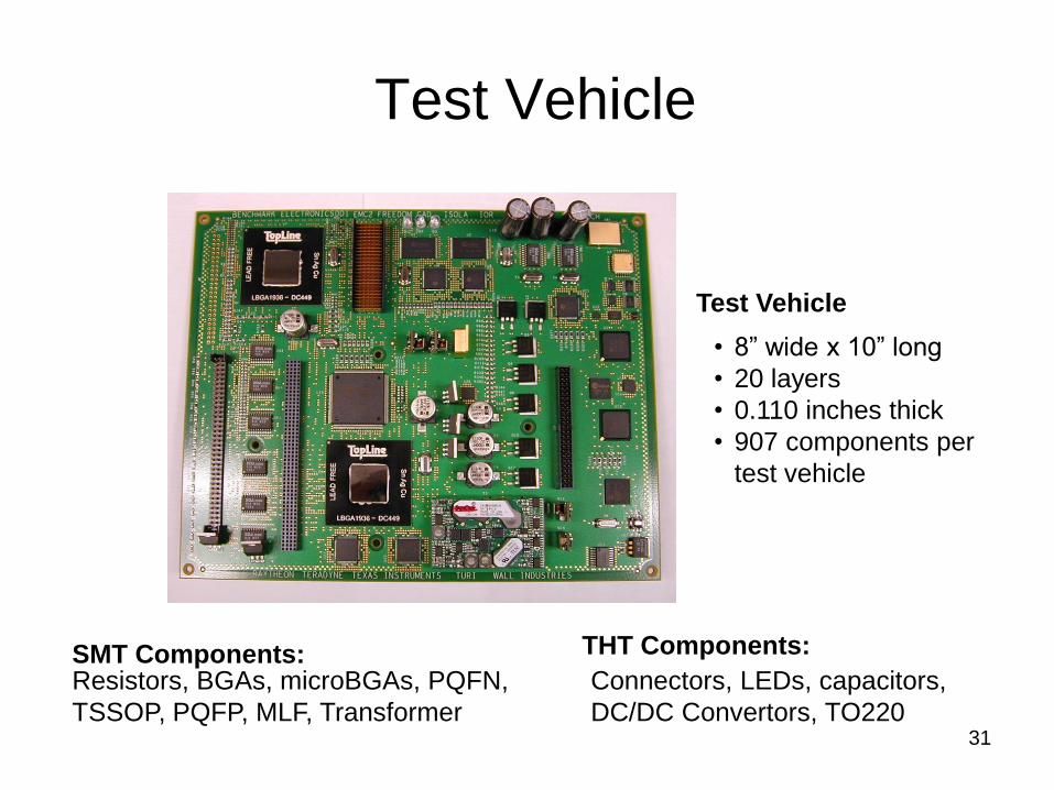
Test Vehicle
• 8” wide x 10” long
• 20 layers
• 0.110 inches thick
• 907 components per
test vehicle
SMT Components: THT Components:
Connectors, LEDs, capacitors,
DC/DC Convertors, TO220
Resistors, BGAs, microBGAs, PQFN,
TSSOP, PQFP, MLF, Transformer
Test Vehicle
32
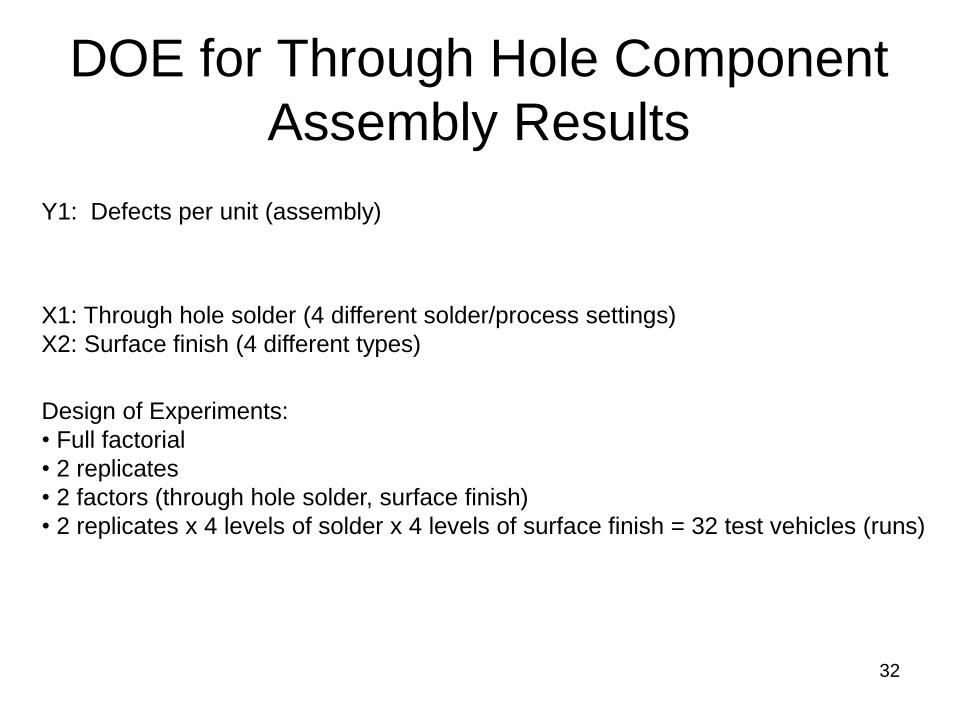
DOE for Through Hole Component
Assembly Results
Y1: Defects per unit (assembly)
X1: Through hole solder (4 different solder/process settings)
X2: Surface finish (4 different types)
Design of Experiments:
• Full factorial
• 2 replicates
• 2 factors (through hole solder, surface finish)
• 2 replicates x 4 levels of solder x 4 levels of surface finish = 32 test vehicles (runs)
33
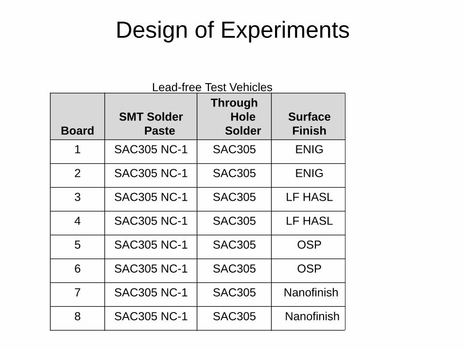
Design of Experiments
Board
SMT Solder
Paste
Through
Hole
Solder
Surface
Finish PWB Laminate
1 SAC305 NC-1 SAC305 ENIG High Tg FR4
2 SAC305 NC-1 SAC305 ENIG High Tg FR4
3 SAC305 NC-1 SAC305 LF HASL High Tg FR4
4 SAC305 NC-1 SAC305 LF HASL High Tg FR4
5 SAC305 NC-1 SAC305 OSP High Tg FR4
6 SAC305 NC-1 SAC305 OSP High Tg FR4
7 SAC305 NC-1 SAC305 Nanofinish High Tg FR4
8 SAC305 NC-1 SAC305 Nanofinish High Tg FR4
Lead-free Test Vehicles
34
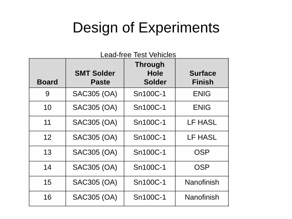
Design of Experiments
Board
SMT Solder
Paste
Through
Hole
Solder
Surface
Finish PWB Laminate
9 SAC305 (OA) Sn100C-1 ENIG High Tg FR4
10 SAC305 (OA) Sn100C-1 ENIG High Tg FR4
11 SAC305 (OA) Sn100C-1 LF HASL High Tg FR4
12 SAC305 (OA) Sn100C-1 LF HASL High Tg FR4
13 SAC305 (OA) Sn100C-1 OSP High Tg FR4
14 SAC305 (OA) Sn100C-1 OSP High Tg FR4
15 SAC305 (OA) Sn100C-1 Nanofinish High Tg FR4
16 SAC305 (OA) Sn100C-1 Nanofinish High Tg FR4
Lead-free Test Vehicles
35
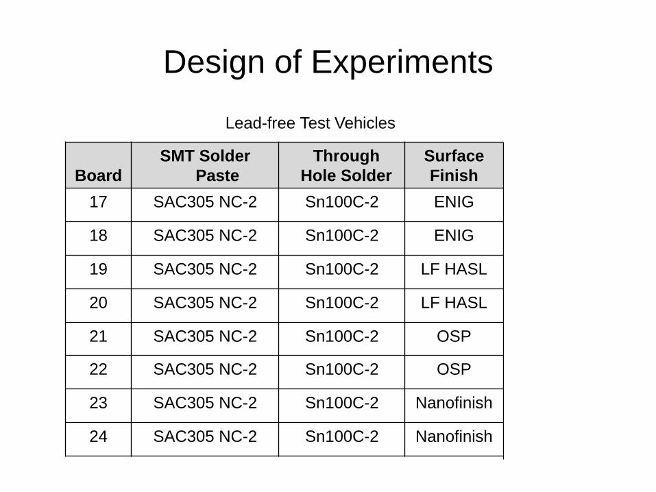
Design of Experiments
Board
SMT Solder
Paste
Through
Hole Solder
Surface
Finish PWB Laminate
17 SAC305 NC-2 Sn100C-2 ENIG High Tg FR4
18 SAC305 NC-2 Sn100C-2 ENIG High Tg FR4
19 SAC305 NC-2 Sn100C-2 LF HASL High Tg FR4
20 SAC305 NC-2 Sn100C-2 LF HASL High Tg FR4
21 SAC305 NC-2 Sn100C-2 OSP High Tg FR4
22 SAC305 NC-2 Sn100C-2 OSP High Tg FR4
23 SAC305 NC-2 Sn100C-2 Nanofinish High Tg FR4
24 SAC305 NC-2 Sn100C-2 Nanofinish High Tg FR4
Lead-free Test Vehicles
36
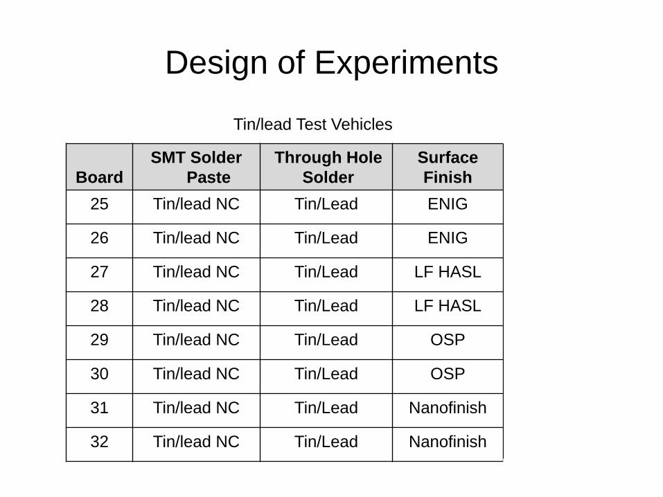
Design of Experiments
Board
SMT Solder
Paste
Through Hole
Solder
Surface
Finish PWB Laminate
25 Tin/lead NC Tin/Lead ENIG High Tg FR4
26 Tin/lead NC Tin/Lead ENIG High Tg FR4
27 Tin/lead NC Tin/Lead LF HASL High Tg FR4
28 Tin/lead NC Tin/Lead LF HASL High Tg FR4
29 Tin/lead NC Tin/Lead OSP High Tg FR4
30 Tin/lead NC Tin/Lead OSP High Tg FR4
31 Tin/lead NC Tin/Lead Nanofinish High Tg FR4
32 Tin/lead NC Tin/Lead Nanofinish High Tg FR4
Tin/lead Test Vehicles
37
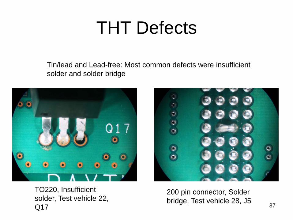
THT Defects
TO220, Insufficient
solder, Test vehicle 22,
Q17
200 pin connector, Solder
bridge, Test vehicle 28, J5
Tin/lead and Lead-free: Most common defects were insufficient
solder and solder bridge

38
Assembly Results:
THT Component Main Effects M
ea
n o
f TH
T D
efe
cts
Tin/LeadSn100C (2)Sn100C (1)SAC 305
140
130
120
110
100
90
80
70
60
50
OSPNanoLF HASLENIG
THT Solder Surface Finish
Main Effects Plot (data means) for THT Defects
• Sn100C (1) had the lowest defect rate for all solders
• Lead-free HASL had the lowest defect rate for all surface finishes
39
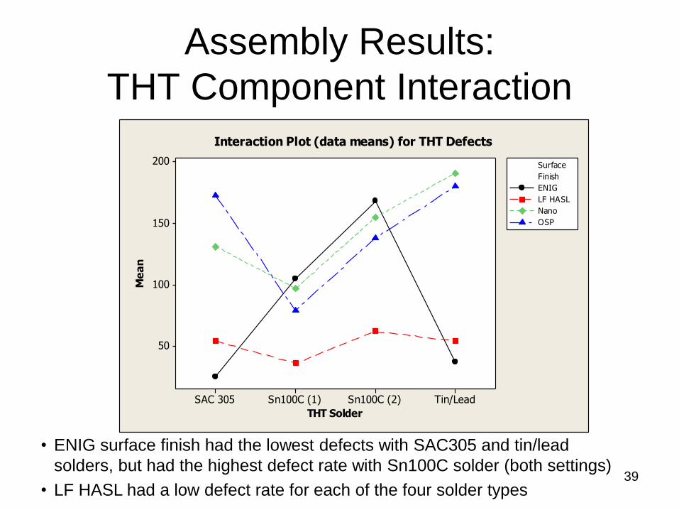
Assembly Results:
THT Component Interaction
THT Solder
Me
an
Tin/LeadSn100C (2)Sn100C (1)SAC 305
200
150
100
50
ENIG
LF HASL
Nano
OSP
Finish
Surface
Interaction Plot (data means) for THT Defects
• ENIG surface finish had the lowest defects with SAC305 and tin/lead
solders, but had the highest defect rate with Sn100C solder (both settings)
• LF HASL had a low defect rate for each of the four solder types
40
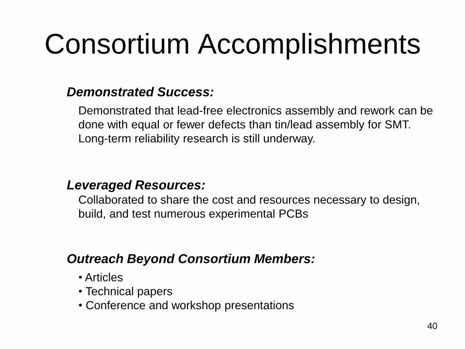
Consortium Accomplishments
Collaborated to share the cost and resources necessary to design,
build, and test numerous experimental PCBs
Demonstrated that lead-free electronics assembly and rework can be
done with equal or fewer defects than tin/lead assembly for SMT.
Long-term reliability research is still underway.
Leveraged Resources:
Demonstrated Success:
Outreach Beyond Consortium Members:
• Articles
• Technical papers
• Conference and workshop presentations

41
Consortium Member Benefits
Academia:
Forged collaborative relationships between university
and regional businesses.
Provided real world learning opportunities for graduate
and undergraduate students.
Increased university faculty experience in applied
science and engineering.
42
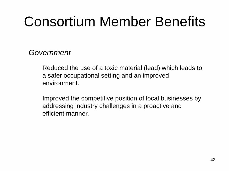
Consortium Member Benefits
Government
Reduced the use of a toxic material (lead) which leads to
a safer occupational setting and an improved
environment.
Improved the competitive position of local businesses by
addressing industry challenges in a proactive and
efficient manner.

43
Consortium Member Benefits
Industry
Ability to have input and influence on consortium efforts (e.g.
material selection, supplier selection, testing strategies, etc.).
Access to cutting edge research and analysis.
Ability to share the costs to address a major industry challenge.
Forum provided to share ideas and receive advice from industry
peers.
Ability to derive competitive advantage for early preparedness.
Individual: Become a knowledge leader within organization.

44
Thank you.
For any questions, contact:
Gregory Morose, Sc.D.
Industry Research Project Manager
Toxics Use Reduction Institute
www.turi.org
University of Massachusetts Lowell
Phone: 978-934-2954