Embed Size (px)
Citation preview

IFM - Department of Physics, Chemistry and Biology
Master of Science Thesis
A Combinatorial Chemistry Approach tothe Amorphous Al-In-Zn-O Transparent
Oxide Semiconductor System
Pär Arumskog
A diploma work with
The Plasma & Coatings Physics Division
2012-06-15
LITH-IFM-A-EX–12/2694–SE
Department of Physics, Chemistry and Biology
Linköping University
SE-581 83 Linköping, Sweden

IFM - Department of Physics, Chemistry and Biology
Master of Science Thesis
A Combinatorial Chemistry Approach tothe Amorphous Al-In-Zn-O Transparent
Oxide Semiconductor System
Pär Arumskog
A diploma work with
The Plasma & Coatings Physics Division
2012-06-15
SUPERVISOR
Dr. Kostas Sarakinos
EXAMINER
Professor Ulf Helmersson

Presentation Date 2012-06-15
Publishing Date (Electronic version) 2012-
Department and Division Plasma & Coating Physics Division Department of Physics, Chemistry and Biology Linköpings universitet, SE-581 83 Linköping
URL, Electronic Version http://urn.kb.se/resolve?urn=urn:nbn:se:liu:diva-xxxx
Publication Title A Combinatorial Chemistry Approach to the Amorphous Al-In-Zn-O Transparent Oxide Semiconductor System
Author(s) Pär Arumskog
Abstract This report describes the successful application of a combinatorial chemistry approach to the evaluation of the amorphous transparent oxide semiconductor Al-In-Zn-O, a-AIZO, for use as channel layers in thin film transistors, TFTs. Many technologies, such as computing and electronic displays, rely on the use of the transistor. In particular, for flat panel displays, the development of new TFTs for the control electronics are necessary for thinner displays with better resolution. In addition, transparent materials deposited at low temperatures would enable a new range of applications. To accomplish this, new materials for the TFT channel layer are needed.
Transparent oxide semiconductors (TOS) are one alternative the silicon based materials currently in use and the first TOS, amorphous In-Ga-Zn-O, has just gone into production. However, despite its good properties, it suffers from the disadvantage of containing the scarce and expensive metals In and Ga. Several attempts have been made to replace Ga with Al but no systematic study of a-AIZO has been reported. This report describes such a study, using a method known as combinatorial chemistry.
Initially, a-AIZO thin films with composition gradients were deposited by DC/RF magnetron sputtering and, following characterization, TFTs with a variety of a-AIZO channel layer composition were manufactured and investigated. Two different compositional areas were found to yield TFTs with good characteristics.
Keywords Transparent oxide semiconductors, TOS, amorphous TOS, TAOS, combinatorial chemistry, Al-In-Zn-O, AIZO, a-AIZO, IAZO
Language
X English Other (specify below)
Number of Pages
Type of Publication
Licentiate thesis X Degree thesis Thesis C-level Thesis D-level Report Other (specify below)
ISBN (Licentiate thesis)
ISRN: LITH-IFM-A-EX—12/2694--SE
Title of series (Licentiate thesis)
Series number/ISSN (Licentiate thesis)

Abstract
This report describes the successful application of a combinatorial chemistryapproach to the evaluation of the amorphous transparent oxide semiconductorAl-In-Zn-O, a-AIZO, for use as channel layers in thin film transistors, TFTs. Manytechnologies, such as computing and electronic displays, rely on the use of thetransistor. In particular, for flat panel displays, the development of new TFTs forthe control electronics are necessary for thinner displays with better resolution.In addition, transparent materials deposited at low temperatures would enablea new range of applications. To accomplish this, new materials for the TFTchannel layer are needed.
Transparent oxide semiconductors (TOS) are one alternative to the siliconbased materials currently in use and the first TOS, amorphous In-Ga-Zn-O, hasjust gone into production. However, despite its good properties, it suffers fromthe disadvantage of containing the scarce and expensive metals In and Ga. Sev-eral attempts have been made to replace Ga with Al but no systematic study ofa-AIZO has been reported. This report describes such a study, using a methodknown as combinatorial chemistry.
Initially, a-AIZO thin films with composition gradients were deposited byDC/RF magnetron sputtering and, following characterization, TFTs with a vari-ety of a-AIZO channel layer composition were manufactured and investigated.Two different compositional areas were found to yield TFTs with good charac-teristics.

Acknowledgements
I would like to thank all of those who have helped me during my thesis work.I am grateful for the support I have recieved from all the people of the Plasma& Coating Division. I would like to thank my examiner Ulf Helmersson and mysupervisor Kostas Sarakinos for giving me this opportunity. I thank Kostas for hishelpful, professional and quick comments on my report. I thank Sankara Pillayfor his support in getting me both to and from Japan and Daniel Magnefält fortaking of his time to help me learn the art of magnetron sputtering in what iscalled the clean room.
I would also like to thank the Inorganic Materials R&D Department at theSumitomo Electric Industries Ltd. factility in Itami, Japan, and especially theperson responsible for my internship Dr. Yoshida, my supervisor at SumitomoMrs Miyanaga, Mr Awata and Mr Kurisu. For the long hours spent in the labtogether I would also like to extend my gratitude to Mr Kono of the support staff.Finally, I would like to thank the people at Sumitomo Electric for welcoming meto their company and making my stay a memorable one.
Those not mentioned here are not forgotten, neither is their support.
i

Contents
1 Introduction 11.1 Background and Motivation . . . . . . . . . . . . . . . . . . . . . 11.2 Aim and Research Strategy . . . . . . . . . . . . . . . . . . . . . . 31.3 On the Report . . . . . . . . . . . . . . . . . . . . . . . . . . . . . 4
2 Theory 52.1 Introduction to Thin Films . . . . . . . . . . . . . . . . . . . . . . 5
2.1.1 Nucleation and Growth . . . . . . . . . . . . . . . . . . . 52.1.2 Sputtering . . . . . . . . . . . . . . . . . . . . . . . . . . . 62.1.3 Combinatorial Chemistry Approach . . . . . . . . . . . . . 8
2.2 Introduction to Transparent Oxide Semiconductors . . . . . . . . 102.3 Characterization Techniques . . . . . . . . . . . . . . . . . . . . . 11
2.3.1 Stylus Profilometer . . . . . . . . . . . . . . . . . . . . . . 112.3.2 Scanning Electron Microscope and Energy Dispersive X-
ray Spectroscopy . . . . . . . . . . . . . . . . . . . . . . . 122.3.3 Rutherford Backscattering Spectroscopy . . . . . . . . . . 122.3.4 Electrical Transport Properties and the Hall Effect . . . . . 132.3.5 Photolithography . . . . . . . . . . . . . . . . . . . . . . . 142.3.6 Thin Film Transistor Characteristics . . . . . . . . . . . . 15
3 Experiments 163.1 Depositions . . . . . . . . . . . . . . . . . . . . . . . . . . . . . . 16
3.1.1 Deposition system . . . . . . . . . . . . . . . . . . . . . . 163.1.2 Determination of Deposition Rates . . . . . . . . . . . . . 163.1.3 Sample Depositions . . . . . . . . . . . . . . . . . . . . . 16
3.2 Sample Characterization . . . . . . . . . . . . . . . . . . . . . . . 183.2.1 Scanning Electron Microscope and Energy Dispersive X-
ray Spectroscopy . . . . . . . . . . . . . . . . . . . . . . . 183.2.2 Rutherford Backscattering Spectroscopy . . . . . . . . . . 183.2.3 Hall Effect Measurements . . . . . . . . . . . . . . . . . . 18
3.3 Thin Film Transistors . . . . . . . . . . . . . . . . . . . . . . . . . 183.3.1 Thin Film Transistor Fabrication Process . . . . . . . . . . 183.3.2 Thin Film Transistor Characteristics Measurements . . . . 19
4 Results 204.1 Depositions . . . . . . . . . . . . . . . . . . . . . . . . . . . . . . 20
4.1.1 Film Appearance . . . . . . . . . . . . . . . . . . . . . . . 204.2 Sample Characterization . . . . . . . . . . . . . . . . . . . . . . . 21
ii

4.2.1 Film Thickness . . . . . . . . . . . . . . . . . . . . . . . . 214.2.2 Chemical Composition . . . . . . . . . . . . . . . . . . . . 214.2.3 Electrical and Transport Properties . . . . . . . . . . . . . 234.2.4 Thin Film Transistor Fabrication and Characteristics . . . . 27
5 Discussion 315.1 Depositions . . . . . . . . . . . . . . . . . . . . . . . . . . . . . . 315.2 Sample Characterization . . . . . . . . . . . . . . . . . . . . . . . 31
5.2.1 Chemical Composition . . . . . . . . . . . . . . . . . . . . 315.2.2 Electrical and Transport Properties . . . . . . . . . . . . . 325.2.3 Thin Film Transistor Characteristics . . . . . . . . . . . . . 325.2.4 Thin Film Transistor Characteristics and Hall Effect Mea-
surements . . . . . . . . . . . . . . . . . . . . . . . . . . . 33
6 Summary and Outlook 34
iii

List of Tables
3.1 Substrate-target distances . . . . . . . . . . . . . . . . . . . . . . 173.2 Sample deposition conditions . . . . . . . . . . . . . . . . . . . . 173.3 RBS measurement uncertainties and detection limits. . . . . . . 183.4 TFT characteristics measurement conditions . . . . . . . . . . . . 19
4.1 Comparison between composition measurements performed withSEM-EDX and RBS . . . . . . . . . . . . . . . . . . . . . . . . . . 23
4.2 Electrical and transport properties for the low Al part of the 0%O2 sample . . . . . . . . . . . . . . . . . . . . . . . . . . . . . . . 23
iv

List of Figures
1.1 Schematic of a TFT . . . . . . . . . . . . . . . . . . . . . . . . . . 2
2.1 Schematic diagram of total system free energy vs the radius r ofa spherical nucleus in a homogeneous fluid . . . . . . . . . . . . 7
2.2 Schematic of the sputtering process . . . . . . . . . . . . . . . . . 92.3 Illustration of the combinatorial chemistry method . . . . . . . . 102.4 Illustration of the band structure of a material . . . . . . . . . . . 122.5 SEM electron beam interaction with the sample volume . . . . . 132.6 Scattering geometry of an RBS experiment . . . . . . . . . . . . . 142.7 Illustration of the Hall effect for electrons . . . . . . . . . . . . . 152.8 Illustration of ideal TFT output and transfer characteristics. . . . 15
4.1 Film appearance . . . . . . . . . . . . . . . . . . . . . . . . . . . 204.2 Film thickness for both 500 nm samples . . . . . . . . . . . . . . 224.3 Chemical composition in the 0% O2 sample. . . . . . . . . . . . 244.4 Chemical composition in the 6.7% O2 sample. . . . . . . . . . . 254.5 Measured part of the ternary diagram for the 0% O2 sample . . . 264.6 Hall effect mobility, µH [cm2/V s], against composition . . . . . . 274.7 Carrier concentration, N [cm−3], against composition . . . . . . 284.8 Resistivity, ρ [Ωcm], against composition . . . . . . . . . . . . . . 294.9 Photograph and SEM image of the TFTs . . . . . . . . . . . . . . 294.10 Classification of TFTs . . . . . . . . . . . . . . . . . . . . . . . . . 30
v

Chapter 1
Introduction
1.1 Background and Motivation
Electronic displays are already ubiquitous in the modern world and the numberand quality of them are constantly increasing. Flat panel display (FPD) tech-nology is currently developing rapidly and new advances promises thinner andlighter displays with better resolution. In addition, the goal of much researchlately has been to develop flexible and transparent displays. This would en-able a range of exciting applications, such as converting the windscreen of a carinto a transparent screen, a tablet computer that can be rolled up and wearableelectronics. To enable this development and drive it forward, new materials areneeded to form the components of these future displays.
In a FPD, the light usually travels from the backlight through a liquid crystallayer and then passes through a colour filter before reaching the eye of thebeholder. If light is let through or not is controlled by electronics in the backplane of the FPD. The main component here is the transistor, the basis of moderndigital electronics.
At their lowest level, all digital electronic devices ultimately deal with onesand zeros. This is physically performed by transistors. There are many variantsof transistors but the transistors in this report is so-called metal oxide semi-conductor field effect transistors (MOSFET). A MOSFET transistor consists ofa conducting gate electrode and a semiconducting channel layer separated byan insulating gate oxide. In addition, a transistor has two regions of oppositedoping compared to the transistor substrate, known as source and drain. Theseare positioned on either side of the channel layer. Opposite doping means thatif the Si substrate is p-doped (electron deficient), the source and drain will ben-doped (electron rich), and the other way around. A transistor constructed outof thin film layers are known as a thin film transistor or TFT, a schematic pictureof which can be found in figure 1.1. In a research setting , it has traditionallybeen common to employ a silicon substrate as gate with an SiO2 layer actingas gate oxide. However, SiO2 has a low dielectric constant κ, resulting in a lowgate oxide capacitance and thereby also a high voltage at which the transistorbegins to enter the ’on’ state, the threshold voltage VT , and a low maximum cur-rent flowing between source and drain, the so-called saturation current Id(sat).As a low VT and a high Id(sat) is desired for most devices, SiO2 has been largely
1

Gate
(Si wafer)
Gate oxide(SiO2)
Channel layer (a-AIZO)
Source Drain
Figure 1.1: Schematic of a TFT. Note that this is a bottom-gate TFT and thematerials indicated are those used in this report.
replaced by higher-κ oxides such as HfO2. [1]The gate and channel layers of most FPD transistors are silicon-based. This
usually means either amorphous hydrogenated silicon (a-Si:H) or polycrystallinesilicon. a-Si:H can be deposited at temperatures below 350°C but suffers fromlow mobility and instability under illumination and electrical bias stress. Poly-crystalline Si on the other hand offer excellent mobility and stability. However,to lower deposition temperatures sufficiently, excimer laser annealing must beused to crystallize the silicon and this has the drawback of resulting in inhomo-geneous crystallization with long-range variations in grain sizes. In addition,polycrystalline silicon suffers from short-range variations in electrical propertiesdue to grain boundaries. [2] There are several problems with the existence ofgrain boundaries; electrical properties will vary between the inside of the grainand along the grain boundary and, due to the fact that different grains have dif-ferent crystallographic orientations and therefore also different electrical prop-erties in a given direction, the electrical properties might change suddenly andwill therefore be difficult to predict or replicate.
To resolve these issues, the search for alternatives to Si-based channel layershas attracted substantial research attention. Alternatives include transparentsemiconducting oxides (TOS) and organic semiconductors. One of the first ofthese alternatives to go into production was the amorphous TOS indium gal-lium zinc oxide (a-IGZO). Although the mobility of a-IGZO is lower than thatof polycrystalline silicon, it does offers higher mobility and better stability thana-Si:H. a-IGZO can also be deposited at low temperatures, room temperatureto 400°C, on glass or plastic substrates. Furthermore, the amorphousness ofa-IGZO means that grain boundary problems are eliminated, giving excellentuniformity.
A common way of growing films of a-IGZO is by a method known as sput-tering. In sputtering, atoms are ejected from a target material by atomic bom-bardment and transferred to the vapor state from which it, in turn, is depositedas a film on a substrate. Because sputtering is one of the standard techniquesused in the semiconductor industry to manufacture TFTs [2] compatibility withthis deposition method would facilitate a transition to a-IGZO.
However, one of the current problems facing the semiconductor industry isthe need to reduce the use of scarce and expensive elements such as In and Ga inits products in order to obtain a cheaper and more sustainable production. The
2

inclusion of In and Ga in a-IGZO is perhaps the main drawback of this material.One of the possible candidates for replacing Ga is Al, having the same valencyas Ga and sharing the strong affinity for oxygen while being a cheap and readilyavailable material. As a comparison, as of May 2012 the price of In and Ga wasover 500 USD/kg while Zn, Al and Si all sold for less than 2 USD/kg. While goldis many times as expensive, silver sells for 900 USD/kg and Ti for 25 USD/kg.[3]
Furthermore, the abundance of Al in the Earth’s crust is 8.23%, Zn 70 ppm,Ga 19 ppm, In 0.25 ppm [4]. In addition, price depends on ease of produc-tion. While aluminium and zinc can be mined as ores, gallium is produced asa byproduct of this production. Indium is also mainly produced as a byproductof zinc mining. For 2011, the United States Geological Survey estimated worldproduction of aluminium to 44.1 million tonnes and of zinc to 12.4 milliontonnes while primary production of gallium was estimated to be a mere 216tonnes (310 including recycling) and that of indium to 640 tonnes (exceeding1800 tonnes if recycling is included) [5].
There have been some research devoted to the TOS aluminium indium zincoxide (AIZO) although this has focused mainly on lightly doped ZnO [6, 7, 8] orInZnO [9]. Also, much of the research has concerned crystalline AIZO [6, 7, 8].Research done on AIZO include deposition by means of direct current sputtering[10, 11], radio frequency alternating current sputtering [12], solution process-ing [9], pulsed laser deposition [6, 7, 8, 13] and the manufacture of organiclight-emitting diodes [10] and capacitors [6, 8, 13]. Furthermore, attemptshave been made to clarify the role of the different elements [11, 12]. Also,a dual-channel AIZO/IZO TFT has been manufactured [9] although a workingTFT with a pure AIZO channel has yet to be reported. However, until now, nosystematic approach to investigating the amorphous Al-In-Zn-O system has beenpublished.
1.2 Aim and Research Strategy
This work aims to take a systematic approach to amorphous AIZO (a-AIZO),investigating a much larger part of the Al-In-Zn ternary phase diagram thanhas previously been done, with the ultimate goal of evaluating the feasibilityof a-AIZO as a TFT channel layer. The objectives are to attempt to elucidatethe influence of composition on electrical properties, followed by an attempt atproducing TFTs with differing channel layer compositions and evaluate these.
The approach chosen here is known as combinatorial chemistry and is ex-plained in detail in Section 2.1.3 on page 8. In keeping with this method, ini-tially an a-AIZO sample with composition gradients is deposited. This sample isdeposited in such a way that the concentration of a given element is maximizedat a sample edge and then decreases across the sample to reach a minimum atthe opposite edge. The maxima of Al, In and Zn form a triangle and the com-positions over the sample represents the ternary phase diagram of these threeelements.
Following deposition, compositions and electrical transport properties of dif-ferent parts of the sample are measured. TFTs are then manufactured with dif-ferent channel layer compositions and the TFT characteristics are measured andevaluated. Finally, all data is analyzed in order attempt to determine the role of
3

the different elements and which, if any, compositions show promising resultsfor use as TFT channel layers.
1.3 On the Report
The work described in this report was performed in cooperation with SumitomoElectric Industries Ltd. and it has been agreed that certain information whichmight affect future research should be excluded from this report.
4

Chapter 2
Theory
2.1 Introduction to Thin Films
Thin films can have a variety of thicknesses, from a single atom layer to mi-crometer thickness. Often, as in this report, they fall in the range between tensand hundreds of nanometers. Thin films can be used to give a bulk material thesurface properties of a different material or, as in the case of a TFT, to constructa very small device layer by layer. Thin films can be deposited by a numberof different techniques. These techniques can in general be divided into thetwo broad categories of chemical vapor deposition (CVD) and physical vapordeposition (PVD). In CVD the solid film is deposited from a chemical vapor byreactions on or in the vicinity of the substrate, which is normally heated. InPVD the source material is initially solid, being transferred to the vapor state byphysical means such as electric, kinetic or thermal energy, before condensing onthe substrate.
2.1.1 Nucleation and Growth
The physical properties of a thin film are ultimately determined by the primarydeposition variables: the film material, the flux J and kinetic energy E of thespecies incident on the substrate, the growth temperature, the flux of contam-inants to the substrate, the substrate material, surface cleanliness, crystallinityand orientation. All these determine the manner in which the film will growand thereby the evolution of its microstructure. [14]
Thermodynamically, the minimum requirement for net deposition on a sur-face is that the condensate pressure P in the gas phase is at least equal toits equilibrium vapor pressure Pvp over the solid of the surface. However, sincesmall clusters of atoms have substantially higher vapor pressures than their bulkcounterparts due to their large surface-to-volume ratio, the supersaturation ra-tio ξ = P/Pvp required is in actuality larger than unity. [14]
The growth of a thin film is initiated by the nucleation of solid clusters (nu-clei) from the vapor or liquid phase. Fluctuations in cluster sizes will enablesome clusters to become stable, i.e. more likely to grow larger than to dis-sociate. Since the surface-to-volume ratio decreases with volume, this occurswhen the energy required to increase the volume of the cluster is offset by the
5

reduction in surface interface area between the cluster and its surroundings.Further cluster growth will thus be thermodynamically favourable. To expressthis formally, the concept of Gibbs free energy need to be introduced. Gibbs freeenergy is a measure of the potentially useful work that could be obtained froma thermodynamic system at constant temperature and pressure. The net freeenergy for the formation of a solid spherical cluster in a homogeneous fluid is
∆G = 4π2γ +4π3∆GV
3(2.1)
where the first term on the right hand side expresses the free energy of theinterface area through the use of the interfacial energy per area, γ, and thesecond term expresses the free energy of the cluster volume. An expression forthe critical cluster size is arrived at by setting d(∆G)
dr = 0 and solving, yielding
r∗ = − 2γ
∆GV(2.2)
Substituting back into (2.1) gives the so-called nucleation activation barrier:
∆G∗ =16γπ3
3G2V
(2.3)
This represents the amount of energy that has to be contributed to form a stablecluster, illustrated in figure 2.1. Naturally, the above discussion is simplified,dealing only with spherical cluster in a homogeneous solution. However, theprinciple still holds although the equations might requires adaptations to beuseful for other cases.
Once a stable cluster has formed, it will grow, both by direct impingementon it by atoms arriving at the surface and by surface diffusion of atoms whichare already present on the surface. Eventually, the cluster will coalesce withneighbouring clusters to form a continuous film.[14]
If, during or after deposition, enough energy is supplied to a material, itsatoms will arrange themselves in a regular manner, forming a lattice. The resultis called a crystal structure and the orientation of the crystal lattice is called thecrystallographic orientation. If all atoms in a film is arranged in the same latticeand is in the same direction, the film is said to be single crystalline whereas ifthe film is composed of regions (grains) of varying crystallographic orientation,it is said to be polycrystalline. A film that lacks crystal structure is said to beamorphous. Such a film has no grains and its surface is smooth and featureless.Amorphous films are formed when there are not enough energy, usually in theform of heat, to form the bonds of the crystal structure.
The energy needed to form crystal structures vary with the bond energies in-volved. Metals have low energy bond and therefore they are found as crystallinesolids even below room temperature. Semiconductors on the other hand havecovalent bonds that require substantially more energy, and thus higher temper-atures, to form. This means that semiconductors grown at room temperaturewill usually be amorphous.
2.1.2 Sputtering
Sputtering is a method for physical vapor deposition (PVD) [15, 14, 16]. It relieson the ejection of atoms or molecules from a surface, called the target, by means
6

Surface energy
Volume free energy
Gibbs free energy
0Cluster radius, r
ΔG*
r*
Total free energy
Figure 2.1: Schematic diagram of total system free energy vs the radius r ofa spherical nucleus in a homogeneous fluid. The total free energy is ∆G =
4π2γ+ 4π3∆GV
3 and the right hand terms are plotted separately as dashed lines,4π2γ being the surface energy and 4π3∆GV
3 the volume free enrgy. The criticalcluster size r∗ and the nucleation barrier ∆G∗ is also shown in the graph.
7

of bombardment by energetic species, usually gaseous ions. The species aresupplied by a plasma and they are then accelerated towards the target surfaceby means of application of a negative electrical voltage to the cathode on whichthe target is mounted. Upon colliding with the target, energy and momentumis transferred to target atoms, ejecting (sputtering) these. The sputtered atomswill then travel away from the target, impinging on the chamber walls or thesubstrate and forming a film. A schematic figure of the sputtering system andprocess can be found in figure 2.2.
Sputtering is always performed in a vacuum chamber and the pressure inthe chamber during deposition is referred to as the working pressure. The gasthat will form the plasma is called the sputtering gas and is introduced into thesputtering chamber after evacuation of the same. The sputtering gas is mostfrequently Ar but other, heavier inert gases such as Kr may also be used. Alongwith the sputtering gas, reactive gas may also be introduced into the chamber,e.g. N2 or O2. This gas will react with the materials on the target surface,forming the material that is to be sputtered. This way it is possible to use ametal target and O2 reactive gas to obtain a metal oxide film on the substrate.This method is called reactive sputtering.
Along with the sputtered atoms, electrons, called secondary electrons alsoleave the surface. The secondary electrons are repelled from the negativelycharged cathode and contribute to the ionization of the plasma. Since a higherionization degree of the plasma increases the number of incident ions andthereby the amount of material sputtered, concentrating the secondary elec-trons close to the target is beneficial for the sputtering rate. In order to ac-complish this a magnetron is used. A magnetron consists of a set of carefullypositioned permanent magnets behind the target cathode. As charged parti-cles moving in a magnetic field, the electrons will experience a force that willcompell them to move in a helical trajectory around the magnetic field lines,thus being trapped closer to the target. This type of sputtering is referred to asmagnetron sputtering.
If the power is applied to the magnetron by means of a direct current, wehave DC magnetron sputtering, whereas if the power is applied by means of analternating current, we have AC magnetron sputtering. When the AC power hasa frequency of 13.56 MHz this is referred to as radio frequency, RF, magnetronsputtering. Sputtering using several magnetrons simultaneously are called co-sputtering and will produce a film containing species from all targets. If bothsubstrate and targets are stationary during deposition, co-sputtering will pro-duce a film with concentration gradients since sputtering depositions only areline-of-sight.
2.1.3 Combinatorial Chemistry Approach
Combinatorial chemistry approaches were developed as an efficient way ofsearching for materials which would have improved performances. Originallyapplied in the pharmaceutical industry, it has now spread to other areas suchas material science. Combinatorial chemistry is basically an approach to large-scale, rapid testing of samples. It involves the synthesis and investigation of alarge number of similar but slightly different samples in order to narrow downfurther research to the most likely candidate(s). In material science the differ-ence could be in composition, crystal structure, growth temperature etc. [17]
8

Substrate
e-
e-e- e-
e-
Magnets
Target
shielding
(grounded)
Target
Gas outlet
(to pump)
Gas
inlet
Secondary
electrons
Sputtered
target atom
Cooling water Power source
Cooling water
Substrate holder (cooling)
Ar+
Ar+ Magnetic
field lines
Electric field
direction
Plasma
(magnetically
confined)
Figure 2.2: Schematic of the sputtering process, here magnetron sputteringusing Ar gas is depicted.
9

Perhaps the simplest variant of the combinatorial method used in materialscience is called natural compositional spread. When employing this method,films are deposited on a large substrate using co-sputtering or a similar tech-nique to obtain a sample with compositional gradients, akin to a ternary phasediagram, as illustrated in figure 2.3. The substrate is divided into a regular pat-tern and for each small area, film composition and other interesting propertiesare measured. The data obtained is then analyzed, enabling the researcher todetermine what effect the composition changes have and what compositions, ifany, are interesting enough to warrant further research. [17]
It is expected that a combinatorial chemistry approach will have the addedadvantage of suppressing the influence of process variation, allowing for a morereliable evaluation of device characteristics. Furthermore, this might be espe-cially clear for amorphous materials since the composition variation can be var-ied continuously unlike a crystalline material where only certain compositionsare allowed. [18]
Figure 2.3: Illustration of the combinatorial chemistry method, here specificallynatural compositional spread. The sample on the left is deposited using co-sputtering from three targets and subdivided into a grid. Measuring the chemi-cal composition of the pieces of the grid enables placing of them in the ternaryphase diagram shown on the right.
2.2 Introduction to Transparent Oxide Semiconduc-tors
Transparent oxide semiconductors have been known for some time but it is onlyrecently, starting in the late 1990s that intensive research has brought themforward as an alternative to conventional semiconductors such as Si, GaAs, InP
10

and GaN. The first report of a ZnO TFT was published in 1968 [19] and at thetime several other oxides were also suggested for use as TFT channel layers, e.g.SnO2 [20, 21] and In2O3. Current research is focused on ZnO, usually dopedwith a variety of dopants and many articles have been published since early2000. [2]
IGZO was pioneered by Professor Hosono of the Tokyo Institute of Technol-ogy [2, 22, 23] and a substantial amount of research has been devoted to itduring the last few years. This includes investigations of deposition techniques[24, 25], influence of process parameters [24, 25, 26] and effect of chemi-cal composition [18] on electronic properties and applied research such as themanufacture and evaluation of TFTs [24, 25, 26, 27].
The requirements for a TOS is obviously that it be an oxide-based trans-parent semiconductor. Transparent here means visually transparent to humans,i.e. it should not absorb light in the wavelength range between 380 and 740nm (photon energies of 1.8 - 3.2 eV) [28]. A semiconductor is usually definedby its band structure. The band structure is formed by the combination of theelectronic orbitals of a material. This results in two bands, called the valence(VB) and the conduction bands (CB), separated by a so-called band gap (Eg),see figure 2.4. Conduction occurs via electrons in the conduction band. In aconductor, the conduction band is partially filled with electrons whereas in aninsulator there are no electrons in the conduction band and the band gap is toolarge to excite any electrons up to the level of the conduction band. A semicon-ductor has a small band gap, enabling excitations of electrons from the valanceband to the conduction band. [29] Furthermore, the optical and electrical prop-erties are not independent but can affect each other [30].
Since conventional semiconductors like silicon have highly directional cova-lent bonds, destroying the crystal structure will drastically reduce carrier mobil-ity, resulting in seriously degraded electronic properties. However, the standardband structure of a TOS is that the valence band consists of the oxygen 2p or-bitals and the conduction band consists of the metal s-orbitals [28]. Due tothe fact that the metal s-orbitals are spherical and therefore overlap regardlessof crystal structure or lack thereof, the carrier mobility of a TOS will survive abreakdown of the crystal structure intact. Thanks to this property of transparentamorphous oxide semiconductors, TAOS, they can be deposited at temperatureslow enough to enable plastic substrates to be used. In addition, this will elimi-nate any grain boundary problems.
In most TOS, oxygen vacancies provide the free carriers needed for conduc-tion, hence the large dependence of TAOS properties on oxygen content. Also,since most TAOS are a mix of different binary oxides, exact composition is cru-cial to device performance when the TAOS is used as a TFT channel layer [26].This has also been demonstrated by a combinatorial approach to a-IGZO [18].
2.3 Characterization Techniques
2.3.1 Stylus Profilometer
A stylus profilometer utilizes a stylus, usually made of diamond, to measuresthe profile of a surface. The stylus is moved vertically till it is in contact withthe surface to be measured and it is then moved horizontally over the surface,
11

E
kEg
CB
VB
Figure 2.4: Illustration of the band structure of a material. Here CB denotesthe conduction band and V B the valence band. Furthermore, E is energy, k isthe wave vector and Eg is the energy gap.
registering the vertical displacement of the stylus as it moves, often relying oninterferometry to do so. A stylus profilometer has the advantage of being largelyindependent of the surface material and can have resolution in the range of tensof nanometers. [31, 32]
2.3.2 Scanning Electron Microscope and Energy DispersiveX-ray Spectroscopy
The scanning electron microscope (SEM) uses electrons to probe samples, imag-ing topography and structure. Electrons are generated in the SEM electron gunand focused on the sample using a series of electromagnetic lenses. The focusedelectron beam scans the sample and the secondary or backscattered electronsare collected and form the SEM image. The electron beam interactions with thesample are illustrated in figure 2.5. [14]
When the electron beam strikes the sample surface, an incoming electronmay excite an electron in an inner shell of a sample atoms, ejecting it. An elec-tron from an outer shell of the atom will fill the empty orbital and in so doingwill emit X-rays of a wavelength characteristic for that element, so-called char-acteristic X-rays. Measuring the energy of these X-rays enables determination ofthe elemental composition of the sample. This analysis technique is referred toas energy dispersive X-ray spectroscopy, EDX.[14]
2.3.3 Rutherford Backscattering Spectroscopy
Rutherford backscattering (RBS) relies on bombarding the sample with ions andmeasuring the elastically backscattered ions to determine the sample composi-tion with depth, see figure 2.6 for a schematic setup. The mass of the sampleatoms are identified by measuring the energy of the backscattered ions usingthe so-called kinematic factor k, defined as E1 = k · E0 where E0 and E1 arethe ion energies before and after collision respectively. The depth at which thescattering occurs is determined by comparing the energy of the backscattered
12
Interaction
volume
Electron
beam
Backscattered
electrons
Secondary
electrons
Cathodoluminescence
Characteristic
X-rays
Sample
volume
Figure 2.5: SEM electron beam interaction with the sample volume. The sizeand shape of the interaction volume depends on the energy of the incidentelectron beam. Note that, unlike e.g. the backscattered electrons that are allscattered close to the surface, the characteristic X-rays originate from the entireinteraction volume and emanate in all directions.
ions with the maximum energy of an ion scattered at the surface using the so-called stopping power S, defined as the mean energy loss per unit path length,S(E) = −dEdx . The amount of an element in the sample is measured by compar-ing the number of ions scattered by atoms of the element in question to the tothe total number of incident ions. Here, the probability of a collision betweenthe incident ion and target atom is determines by the scattering cross sectionσ(θ) ∝ Z2
1Z22
E2 where θ is the scattering angle, Z1 and Z2 is the atomic numbersof the incident ion and the target atom respectively, and E is the energy of theincident ion beam. [33, 34]
When using RBS, the results will be a mixture of mass and depth scales.To separate these, one relies on simulations and match these with the exper-imental data. RBS is a non-destructive analysis technique that requires littlesample preparation. Furthermore, it is very accurate, especially for medium toheavy elements on light substrates, and provides depth perception as well. Thedrawbacks of RBS is its poor sensitivity for elements with low scattering crosssection, low resolution for high Z elements and high cost. [33, 34]
2.3.4 Electrical Transport Properties and the Hall Effect
Charge carriers in semiconductors can in general be both electrons and holes.The number of charge carriers per volume, known as the carrier concentration,and the resistivity are properties that are often of interest when working withTFTs. Another property, related to the earlier, is carrier mobility. Carrier mobil-ity is a measure of how quickly a charge carrier can move through a material
13

Sample
Incident He2+
Normal Angle
Detector~160
Backscattered
He2+
Figure 2.6: Scattering geometry of an RBS experiment. Here, the conditionsdescribed in the experimental section of this report is depicted. In reality, theincident particles can differ from He2+ and the angle to the detector can differslightly.
and it is therefore inversely proportional to the effective mass. The relationbetween the resistivity ρ (Ωcm), the carrier concentration N (cm−3) and themobility μ (cm2/V s) is
ρ =1
q ·N · µ(2.4)
where q is the elemental charge (1.60 · 10−19C). [29]Carrier mobility can be defined and measured in several different ways but
a common way to measure mobility is to use the Hall effect. When a current Iflows in the x-direction in a perpendicular magnetic field BZ directed along thez-axis, an electrical field EY is induced along the negative y-axis, see figure 2.7.The Lorentz force acting on the electrons or holes in the current will acceler-ate them in the negative y-direction, inducing the electric field. The voltageassociated with this induced electrical field is what is called the Hall voltage,VH . Note that both electrons and holes will be accelerated in the same directionsince both their direction of travel and their charge are opposite, canceling theeffect. The sign of the measured voltage will, however, reflect the nature of thecharge carriers. [29]
2.3.5 Photolithography
Photolithography is a technique for selectively removing parts of a thin filmoften used in the fabrication of TFTs. It utilizes UV light to transfer the desiredpattern from a photomask to a light sensitive chemical, known as a photoresistor resist, previously applied to the film. Having exposed the resist to UV light,a developer fluid is used to remove the illuminated resist (in case of a negativeresist), after which the underlying film is etched. In case of a positive resist,the developing process removes the unilluminated parts of the resist instead.Finally, the remaining resist is removed, leaving behind a substrate with onlythe unetched parts of the film remaining. [16]
14

I
BZEY
x
y
ze-
Figure 2.7: Illustration of the Hall effect, here the carriers are electrons. VXis the applied voltage and BZ the applied magnetic field whereas EY is theresulting electric field and VH the measured Hall voltage.
2.3.6 Thin Film Transistor Characteristics
To evaluate a TFT, its so-called output and transfer characteristics are measured.To measure the output or I − V characteristics, the gate voltage VG is fixed, thedrain-source voltage VDS is varied and the drain-source current IDS is mea-sured, resulting in a IDS − VDS curve. Ideally, IDS rises linearly for small VDSand then saturates, the saturation value increasing with increasing VG. To mea-sure the transfer characteristics, the source-drain voltage VDS is fixed, the gatevoltage VG is varied and again, the source-drain current IDS is measured, givinga IDS − VG curve. Ideally, a TFT will have extremely low IDS for negative VG,rising very steeply as VG becomes positive,. However, the slope should decreaserapidly and tend to a saturation value for higher voltages. The ideal shape ofthe IDS − VGS resembles a smoothed step function. Ideal TFT characteristicsare illustrated in figure 2.8.[29]
VG=1 V
VG=2 V
VG=3 V
VG=5 V
VG=10 V
VDS
IDS
Output Characteristic
VG
IDS
0
VDS = fixed
Transfer Characteristic
Figure 2.8: Illustration of ideal TFT output and transfer characteristics.
15

Chapter 3
Experiments
All experiments were performed at the factility of Sumitomo Electric IndustriesLtd. in Itami, Hyogo Prefecture, Japan, unless otherwise stated.
3.1 Depositions
3.1.1 Deposition system
The depositions were performed with a Showa SPH-2302 sputtering systemequipped with three 2 inch (5 cm) magnetrons. The targets used were In2O3,Al2O3, ZnO, all 99.99% purity, thickness 3 mm. The substrate position was inthe chamber centre, equidistant from all targets. The working pressure was0.50 Pa and two different atmospheres were used; a pure Ar atmosphere (30sccm Ar) or a mix of Ar and O (28 sccm Ar, 2 sccm O2). Hereinafter, the samplesdeposited in these atmospheres will be identified by the oxygen content in theatmosphere, i.e. 0% and 6.7% respectively.
3.1.2 Determination of Deposition Rates
To determine the depositions rates of the different targets and to match themwith each other, films were deposited on quartz glass substrates, both over thetarget in question and in the sample position in the centre of the chamber.The quartz glass substrates had a piece of tape taped across them which wereremoved after the deposition, exposing the glass surface. The height differencebetween the film surface and the bare glass surface was then measured using aTokyo Seimitsu Surfcom E-MD-S75B stylus profilometer. The deposition rates,in nm/min, were then calculated for each target and power and substrate-targetdistances were adjusted to achieve the same deposition rate for all three targets.The film thickness of the samples described in Section 3.1.3 were also verifiedusing the same profilometer.
3.1.3 Sample Depositions
Following matching of the deposition rates of the three targets, the a-AIZO sam-ples were deposited. For the sample depositions, SiO2 terminated (111) ori-
16

ented p-doped (Boron) Si wafers with a diameter of 4 inches (100 mm) wasused as substrates. The SiO2 layer was produced by thermal oxidation and hada thickness of 100 nm. All three targets as well as the substrate were watercooled. Before sample depositions, the chamber was evacuated to < 7.0 · 10−5
Pa. The targets were pre-sputtered for 10 minutes at the same target powersused during deposition (see table 3.2). A total of 4 samples were deposited.Two with target thickness of 500 nm and two with target thickness of 70 nm. Inboth cases, the samples with the same thickness were deposited in different de-position atmospheres. The 500 nm samples were deposited to be used for Halleffect measurements and the 70 nm samples were to be used to manufactureTFTs. The 500 nm samples were deposited with a metal mask shadowing partsof the substrate and giving rise to a grid pattern where each small square wereto become a small sample.
The deposition conditions were chosen after the deposition rates of the tar-gets had been matched, as described above, and deposition conditions for allsamples can be found in tables 3.1 and 3.2.
Table 3.1: Substrate-target distances
Target S-T distance [mm]
Al2O3 63
In2O3 108
ZnO 87
Table 3.2: Sample deposition conditions
Sample Target powers Gas flows Deposition time Substrate
70 nm0% O2
In2O3: 40W DCAl2O3: 150W RF
ZnO: 45W RF
Ar: 30 sccmO2: 0 sccm
6 min Si wafer,d=100 mm
70 nm6.7% O2
In2O3: 25W DCAl2O3: 150W RF
ZnO: 20W RF
Ar: 28 sccmO2: 2 sccm
23 min 20 s Si wafer,d=100 mm
500 nm0% O2
In2O3: 40 W DCAl2O3: 150W RF
ZnO: 45W RF
Ar: 30 sccmO2: 0 sccm
41 min 40 s Si wafer,d=100 mm,with metal
mask
500 nm6.7% O2
In2O3: 25W DCAl2O3: 150W RF
ZnO: 20W RF
Ar: 28 sccmO2: 2 sccm
2 h 46 min 40 s Si wafer,d=100 mm,with metal
mask
17

3.2 Sample Characterization
3.2.1 Scanning Electron Microscope and Energy DispersiveX-ray Spectroscopy
Measurements were performed using a JEOL JSM-6490LV SEM system witha Bruker AXS Microanalysis GmbH XFlash QUANTAX EDX. Only the 500 nmsamples were measured and the measurements were made in the middle of thesquares that constituted the grid pattern.
3.2.2 Rutherford Backscattering Spectroscopy
RBS measurements were only performed on two small samples from the 0% O2
500 nm wafer. These samples were selected after evaluation of the Hall effectmeasurements. The measurements were performed by Evans Analytical Group,CA, USA, using a He2+ ion beam of energy 2.275 MeV and a normal detectorangle of 160°. The measurements uncertainties and detection limits for theelements contained in the thin film are listed in table 3.3.
Table 3.3: RBS measurement uncertainties and detection limits.
Element Uncertainty (at%) Detection limit (at%)
Al ±1 1
In ±0.3 0.2
Zn ±1 0.5
O ±4 4
3.2.3 Hall Effect Measurements
The 500 nm samples were cut according to the metal mask grid pattern andsent for measurements at Hyogo Prefectural Institute of Technology, Japan. Theoutermost parts of the grid very close to the wafer edge were not sent for anal-ysis. The measurements were performed at room temperature with a magneticfield of 0.508 T. The current was adjusted according to each sample measured.
3.3 Thin Film Transistors
3.3.1 Thin Film Transistor Fabrication Process
For the TFTs, the Si-substrate was used as gate, the SiO2 (100 nm) as gate oxide,a-AIZO as channel layer and Mo electrodes (100 nm) as source and drain. The6.7% O2 70 nm samples were first cut in a grid pattern, the pieces were thenannealed at 350°C in air for 1h. Photolithography was used to produce AIZOislands, electrodes were deposited by sputtering at Nara Institute of Science andTechnology, Japan, and finally the samples were once again annealed at 300°Cin N2 for 2h.
18

Photolithography process:
The samples were initially cleaned and spin-coated with positive resist (com-mercially available AZ5214, with adhesion promoter hexamethyldisilazane, HMDS)and prebaked at 110°C, before being exposed to UV light. Following exposure,the samples were developed with the commercially available AZ300 developer.The exposed a-AIZO was etched with a phosphoric acid (H3PO4) and acetic acid(CH3COOH) aqueous solution after which the remaining resist was removedand the samples cleaned. In order to form the pattering needed to deposit theelectrodes, the samples were then again spin-coated with AZ5214 resist andprebaked before being exposed to UV light and developed using AZ300 devel-oper.
Electrode depositions:
Mo electrodes were deposited by RF sputtering from a 80 mm in diameter tar-get, target power 100 W, at a S-T distance of 100 mm, using a mask to controlfilm deposition. The working pressure was 0.5 Pa, and the depositions weredone in an Ar gas atmosphere. The electrode thickness was 100 nm.
3.3.2 Thin Film Transistor Characteristics Measurements
The TFT characteristics measurements were performed with a MJC semi-automaticwafer prober AP-80 system and a Agilent Technologies B1500 Semiconductordevice analyzer. For each measuring position, two different TFTs located invery close proximity to each other were measured. For the measurements, thevoltages listed in table 3.4 were used.
Table 3.4: TFT characteristics measurement conditions
Curve Voltage set values Voltage variations
IDS − VDS VG = 0, 1, 2, ..., 10V VDS = 0 ∼ 10V
IDS − VG VDS = 5.1V VG = −10 ∼ 20V
19

Chapter 4
Results
4.1 Depositions
4.1.1 Film Appearance
The 70 nm samples were shiny metallic yellow with slight tints of green andblue. Around the edges of the squares and the wafer edge the blue colour ofthe original SiO2 was visible. The 500 nm samples showed a greater colourvariation; from green to red to violet to yellow from thickest to thinnest partof the film, see figure 4.1. All samples displayed a mirror-like reflection withcoloured tint when viewed at an incident angle close to the surface normal andtotal reflection at low incident angles. Colour variation with film thickness leadto the conclusion that the film itself was transparent. Furthermore, the filmshowed no identifiable surface features in the SEM images, consistent with anamorphous film.
Figure 4.1: Film appearance. Shown here is a 500 nm sample being measuredin the profilometer.
20

4.2 Sample Characterization
4.2.1 Film Thickness
The profilometer thickness measurements, figure 4.2, showed an average thick-ness over the region later measured with the SEM-EDX of 375 nm for the 0% O2
film and 471 nm for the 6.7% O2. Furthermore, the 0% O2 film were thickestclosest to the In2O3 target while the 6.7% O2 film were thickest closest to theAl2O3 target. In the case of the 0% O2, the thinning furthest away from theIn2O3 target might at least partially be attributed to shadowing of the substrateby the substrate holder. This effect is also visible in the 6.7% O2 sample but lesspronounced. The thickness variations did not, however, effect the Hall effectmeasurements (Section 4.2.3 on page 23).
4.2.2 Chemical Composition
The compositional distributions were, as expected, highest closest to the targetand tapered off in a regular manner. The distributions were equally smoothfor both samples, see figure 4.3 and figure 4.4 for the 0% O2 and the 6.7% O2
sample respectively. For the 0% O2 sample, the SEM-EDX measurements indi-cated that there were less In compared to the other metals. In never exceeded47% while Zn were close to and Al over 60%, always assuming that the con-tents of the three metals sum to 100%. However, as previously mentioned, thethickness measurements did not show a thinner film closer to the In target butthe exact opposite. For the 6.7% O2 sample, the maximum Al concentrationreached 65% and the maximum In concentrations exceeded 55%, whereas Zncontent only reached 40%, thus indicating a lower Zn content of the film. Thistime, thickness measurements also showed a thinning of the film close to theZnO target.
In both samples, the oxygen distribution was relatively even, with an aver-age of 59% for 0% O2 and 64% for 6.7% O2. For the 0% O2 the oxygen concen-tration showed slightly lower values close to the ZnO target but this trend wasweaker in the 6.7% O2 sample. The difference between highest and lowest oxy-gen content, taking the content of In, Al, Zn and O to total 100%, was 16.37%for 0% O2 and 12.58% with 6.7% O2.
The RBS results, table 4.1, indicate a quite substantial absolute error in theSEM-EDX results. In general, the SEM results seems to underestimate the Incontent by approximately 25%, overestimate the Al content by approximately20%, and underestimate the Zn content by approximately 5%.
21

1
2
3
4
5
6
7
12
34
56
7
0
200
400
Film Thickness 0% O2
thic
knes
s [n
m]
ZnO
Al2O
3
In2O
3
(a) Film thickness for the 500 nm 0% O2 sample with all three targets marked.
2
4
6
1
2
3
4
5
6
7
0
200
400
600
Film Thickness 6.7% O2
thic
knes
s [n
m]
In2O
3
ZnO
Al2O
3
(b) Film thickness for the 500 nm 6.7% O2 sample with all three targets marked.
Figure 4.2: Film thickness for both 500nm samples. Note that the reason thatthe corner points of the surface has zero thickness is that the substrate wafer isround and hence lacks corners.
22

Table 4.1: Comparison between composition measurements performed withSEM-EDX and RBS on the 500 nm 0% O2 sample. Note that the sample position-column denotes the positions of the sample in the x-y coordinate system of thesubstrate grid pattern.
Sample position Al In Zn
3-2 SEM 24.57 16.24 59.19
3-2 RBS 20.22 22.22 57.56
Δ(SEM/RBS) 122% 73% 103%
5-2 SEM 18.29 27.07 54.64
5-2 RBS 15.58 34.76 49.66
Δ(SEM/RBS) 117% 78% 110%
4.2.3 Electrical and Transport Properties
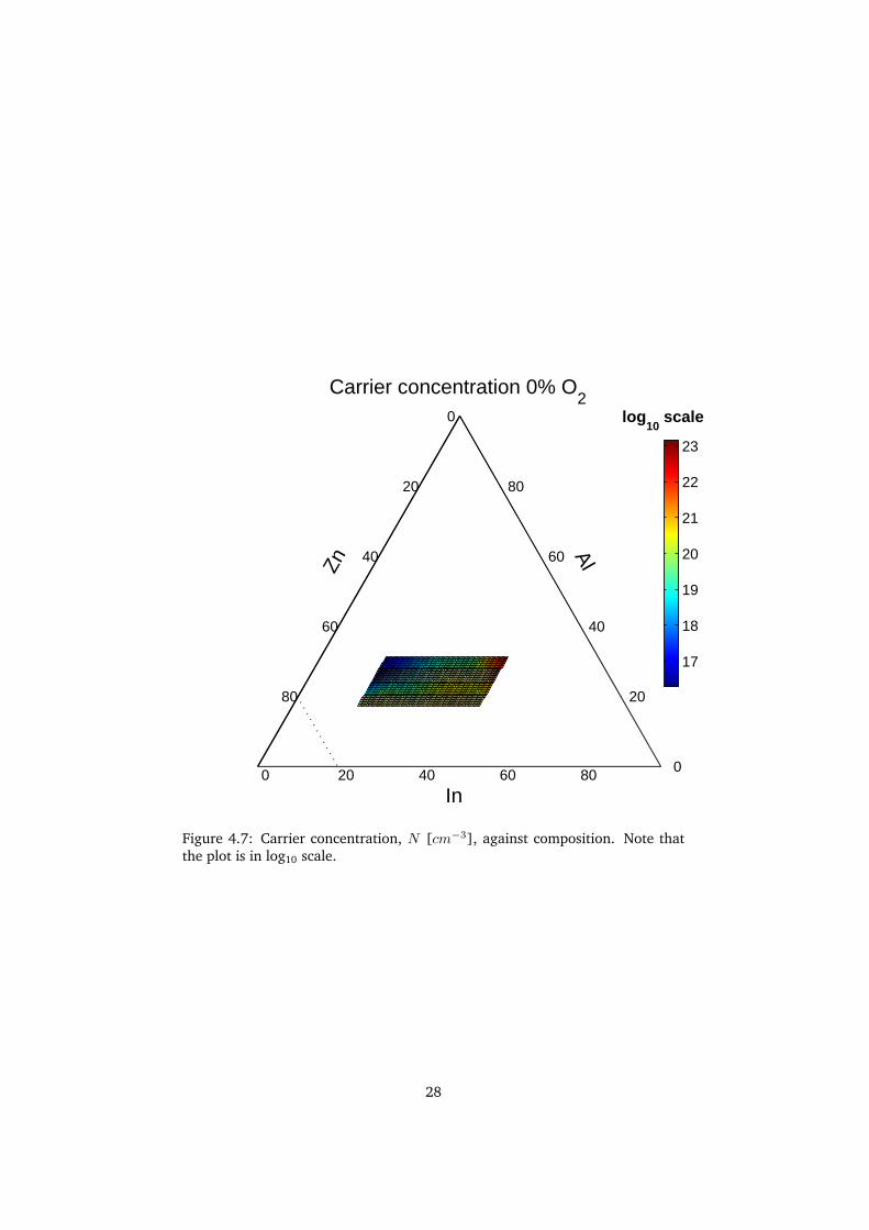
The Hall effect measurements could only be performed for the low Al part ofthe 0% O2 sample, see figure 4.5, and not at all for 6.7% O2 sample. With thenotable exception of two samples with extreme values, the values measured arelisted in table 4.2 together with values for a-IGZO and a-Si:H for comparison.For ternary plots of electrical and transport properties against composition, seefigures 4.6, 4.7, and 4.8.
Table 4.2: Electrical and transport properties for the low Al part of the 0% O2
sample
Hall effect mobilityµH (cm2/V s)
Carrier concentrationN (cm−3)
Resistivityρ (Ωcm)
a-AIZO 0.10− 5.03 1.43 · 1019 − 3.09 · 1020 0.005− 0.905
a-IGZO ∼ 10 1018 − 1020 105 − 107
a-Si:H < 1 1016 − 1017 102 − 104
The two exceptions were Al0.25In0.16Zn0.59O :µH = 514.00 cm2/V s,N =7.44·1016 cm−3, ρ = 0.163 Ωcm andAl0.27In0.44Zn0.29O :µH = 0.10 cm2/V s,N =1.23 · 1021 cm−3, ρ = 0.051 Ωcm. Here it is especially interesting to note the ex-tremely high mobility of Al0.25In0.16Zn0.59O.
However, as the neighbouring sample Al0.21In0.22Zn0.58O only showed amobility of 4.84 and the mobility measured was very unusual, a new sample wasdeposited, this time on a quartz glass substrate to rule out any influence of theSi/SiO2 substrate. The same position on the new sample could not be measuredbut the closest position, Al0.20In0.14Zn0.65O, yielded µH = 3.81 cm2/V s.
Also, although the dependence of electrical and transport properties on com-position was plotted, see figures 4.6, 4.7, 4.8, the effect of the different elementswas not immediately clear except for resistivity which increased with Al. An
23

2
4
6
1 2 3 4 5 6 7
0
20
40
60
Al distribution 0% O2
atom
ic p
erce
nt
Al2O
3
(a) Aluminium distributions as measured by SEM-EDX.
23
45
612345670
10
20
30
40
50
In distribution 0% O2
atom
ic p
erce
nt
In2O
3
(b) Indium distributions as measured by SEM-EDX.
2
3
4
5
6
2
4
6
0
20
40
60
Zn distribution 0% O2
atom
ic p
erce
nt
ZnO
(c) Zinc distributions as measured by SEM-EDX.
Figure 4.3: Chemical composition in the 0% O2 sample.
24

23456
0
2
4
6
8
0
20
40
60
80
Al distribution 6.7% O2
atom
ic p
erce
nt
Al2O
3
(a) Aluminium distribution as measured by SEM-EDX.
2
3
4
5
6
02
46
80
20
40
60
In distribution 6.7% O2
atom
ic p
erce
nt
In2O
3
(b) Indium distribution as measured by SEM-EDX.
2
3
4
5
6 02
46
8
0
20
40
60
Zn distribution 6.7% O2
atom
ic p
erce
nt
ZnO
(c) Zinc distribution as measured by SEM-EDX.
Figure 4.4: Chemical composition in the 6.7% O2 sample.
25

0
20
40
60
80
0 20 40 60 80
0
20
40
60
80
Compositions whose Hall effect were measured, 0% O2
In
AlZ
n
Figure 4.5: Measured part of the ternary diagram for the 0% O2 sample. The(blue) diamonds represent all compositions in the sample as measured by SEM-EDX and the area whose electrical and transport properties could be measuredis delineated by the (purple) hexagon.
26

0
20
40
80
Al 60
80
60
Hall mobility 0% O2
In
0
40
20
40Zn
20
60
80
0
0
1
2
3
4
5
Figure 4.6: Hall effect mobility, µH [cm2/V s], against composition.
attempt at discerning the effect of the different elements indicated that Hallmobility increases with Zn and decreases with Al while carrier concentrationincreases with In and decreases with Zn.
4.2.4 Thin Film Transistor Fabrication and Characteristics
Fabrication proceeded without any major problems, the main difference com-pared to IGZO TFTs being the longer etch time required. Images of the TFTscan be found in figure 4.9. To simplify evaluation, once measured, the TFTcharacteristics were classified according to figure 4.10. Each measured TFTwas assigned a value between 0 and 3 for both characteristics; 0 denoting badresponses, 1 average responses, 2 good responses and 3 the best responses.These values were then summed and finally the average of the two transistorsmeasured for each sample was taken. These results were then mapped to thesubstrate wafer, and then, using the SEM-EDX measurements, to chemical com-position. The TFTs with the best characteristics were obtained in two differentcomposition areas.
27
0
20
Al
40
80
60
80
60
Carrier concentration 0% O2
In
0
40
20
40
20
Zn
60
80
0
17
18
19
20
21
22
23
log10
scale
Figure 4.7: Carrier concentration, N [cm−3], against composition. Note thatthe plot is in log10 scale.
28

0
20
Al
40
80
60
80
60
Resistivity 0% O2
In
0
40
20
40
20
Zn
60
80
0
0
0.2
0.4
0.6
0.8
Figure 4.8: Resistivity, ρ [Ωcm], against composition.
(a) (b)
Figure 4.9: Photograph and SEM image of the TFTs. (a) shows a photograph ofa sample with TFTs. The TFTs are just barely visible with the naked eye. (b) is alow resolution SEM image of the TFTs. The larger black squares are electrodesconnected to the source and drain, the smaller grey squares. The channel layeris visible as a narrow grey stip in the middle of the TFTs.
29

0 2 4 6 8 10-1.0x10⁻¹²
-9.0x10⁻¹³
-8.0x10⁻¹³
-7.0x10⁻¹³
-6.0x10⁻¹³
-5.0x10⁻¹³
-4.0x10⁻¹³
-3.0x10⁻¹³
-2.0x10⁻¹³
-1.0x10⁻¹³
0.01.0x10-13
2.0x10⁻¹³
3.0x10⁻¹³
4.0x10⁻¹³D
rain
sou
rce
curr
ent (
A)
Drain source voltage (V)
Vg = 0 V Vg = 1 V Vg = 2 V Vg = 3 V Vg = 4 V Vg = 5 V Vg = 6 V Vg = 7 V Vg = 8 V
-10 -5 0 5 10 15 20-4.0x10⁻¹²
-2.0x10⁻¹²
0.0
2.0x10⁻¹²
4.0x10⁻¹²
6.0x10⁻¹²
8.0x10⁻¹²
Dra
in s
ourc
e cu
rren
t (A
)
Gate voltage (V)
(a) Bad characteristics: Insulating
0 2 4 6 8 10-2.0x10⁻⁵
0.0
2.0x10⁻⁵
4.0x10⁻⁵
6.0x10⁻⁵
8.0x10⁻⁵
1.0x10⁻⁴
1.2x10⁻⁴
1.4x10⁻⁴
1.6x10⁻⁴
Dra
in s
ourc
e cu
rren
t (A
)
Drain source voltage (V)
Vg = 0 V Vg = 1 V Vg = 2 V Vg = 3 V Vg = 4 V Vg = 5 V Vg = 6 V Vg = 7 V Vg = 8 V
-10 -5 0 5 10 15 206.6x10⁻⁵
6.8x10⁻⁵
7.0x10⁻⁵
7.2x10⁻⁵
7.4x10⁻⁵
7.6x10⁻⁵
7.8x10⁻⁵
8.0x10⁻⁵
8.2x10⁻⁵
8.4x10⁻⁵
8.6x10⁻⁵
8.8x10⁻⁵
Dra
in s
ourc
e cu
rren
t (A
)
Gate voltage (V)
(b) Bad characteristics: Conductive
0 2 4 6 8 10
-5.0x10⁻¹²
0.05.0x10-12
1.0x10⁻¹¹
1.5x10⁻¹¹
2.0x10⁻¹¹
2.5x10⁻¹¹
3.0x10⁻¹¹
3.5x10⁻¹¹
4.0x10⁻¹¹
4.5x10⁻¹¹
5.0x10⁻¹¹
5.5x10⁻¹¹
6.0x10⁻¹¹
6.5x10⁻¹¹
Dra
in s
ourc
e cu
rren
t (A
)
Drain source voltage (V)
Vg = 0 V Vg = 1 V Vg = 2 V Vg = 3 V Vg = 4 V Vg = 5 V Vg = 6 V Vg = 7 V Vg = 8 V Vg = 9 V
-10 -5 0 5 10 15 20
10-14
10-13
10-12
10-11
10-10
10-9
10-8
10-7
Dra
in s
ourc
e cu
rren
t (A
)
Gate voltage (V)
(c) Average characteristics
0 2 4 6 8 10
0.0
2.0x10⁻⁷
4.0x10⁻⁷
6.0x10⁻⁷
8.0x10⁻⁷
1.0x10⁻⁶
1.2x10⁻⁶
Dra
in s
ourc
e cu
rren
t (A
)
Drain source voltage (V)
Vg = 0 V Vg = 1 V Vg = 2 V Vg = 3 V Vg = 4 V Vg = 5 V Vg = 6 V Vg = 7 V Vg = 8 V Vg = 9 V
-10 -5 0 5 10 15 2010-12
10-11
10-10
10-9
10-8
10-7
10-6
10-5
Dra
in s
ourc
e cu
rren
t (A
)
Gate voltage (V)
(d) Good characteristics
Figure 4.10: Classification of TFTs
30

Chapter 5
Discussion
5.1 Depositions
The deposited films showed some thickness variations, probably due to inexactdetermination of the target deposition rates prior to sample deposition. De-termining the deposition rates are time consuming and will ultimately have tobe a compromise between time spent and accuracy. Also, the accuracy of thethickness measurements might very well have suffered due to low resolutionof the profilometer and human error in interpreting the profilometer printouts.However, it is believed that in general the results concerning film thickness iscorrect. In addition, when the profilometer showed results that were unclear orunstable, the measurements were redone, occasionally several times.
For the sample deposition DC power was used for the In2O3 target due toinitial problems with plasma ignition with RF power. It should also be notedthat the oxygen gas flow affects the targets differently, a low oxygen gas flowresulting in blackening of the In2O3 target but being beneficial for the Al2O3
target. However, none of this is expected to cause problems in an industrialprocess as it is then more likely that one will operate with a single target of acertain composition rather than co-sputtering from three targets.
Overall, there were no major problems with the thin film depositions, some-thing that is promising for further research.
5.2 Sample Characterization
5.2.1 Chemical Composition
Since no reference sample was measured, SEM-EDX has to be considered aqualitative technique, not a quantitative one. This means that the absolute el-emental contents of the samples remains uncertain. There are several sourcesof errors in the SEM-EDX measurements. Firstly, the measurements volume islarger than the sample thickness and this will introduce errors into the mea-surements when filtering out the substrate signal. Also, separating the oxygensignal from SiO2 from the a-AIZO oxygen signal is not possible. In addition,after having measured the concentrations of Al, In, Zn and O, the results wererecalculated to discount the O content.
31

The measurements should, however, give us a qualitative picture, enabling acomparison of the amounts of a certain metal at different points of the film andperhaps also comparison of the concentrations of the different metals relativeto each other at a given point on the film. Quantitative measurements, such asRBS, are needed to determine the exact concentrations of any one componentsin the film.
Though the RBS results indicate substantial errors in the SEM-EDX film com-position measurements, a recalculation of the SEM-EDX results to compensatefor the errors would be very uncertain since it would be based on only twomeasurements. Also, while this may be interesting, what is more important isto determine the absolute compositions for the samples that yielded TFTs withgood characteristics.
5.2.2 Electrical and Transport Properties
The Hall effect mobilities were slightly lower than hoped but still demonstratedthat a-AIZO can achieve higher mobilities than a-Si:H and that it might be possi-ble to achieve mobilities comparable to a-IGZO. The resistivities were, however,low for semiconductors. The effect of the different elements were in generaldifficult to determine unequivocally but might have appeared more lucid had alarger part of the sample been possible to measure. However, this depends onmeasurement equipment limitations and while alternatives ways of measuringthe electrical and transport properties, such as raising the temperature, havebeen discussed, the discussion in Section 5.2.4 on the following page cautionsagainst continuous efforts in this respect.
In theory [26, 9], increased In content should result both in increased car-rier concentration and mobility as well as decreasing resistivity. While the mo-bility increase is desired, a too high carrier concentration would give a non-controllable channel conductivity. Al addition would then, similar to the effectof Ga, work to compensate the oxygen vacancies, thereby decreasing the carrierconcentration and giving increased control of channel conductivity. Zn shouldincrease resistivity and decrease mobility. An increase in carrier concentrationand decrease of resistivity with increased In content was seen as well as in-creased resistivity with Al content. However, the effect of Zn was less clear.
The extremely high mobility value measured in one sample could not berepeated and neither were neighbouring values out of the ordinary. Whilst thisproblem may warrant further investigation, the evidence for concluding thatsuch high mobilities are possible in a-AIZO can at the moment not be consideredstrong.
5.2.3 Thin Film Transistor Characteristics
The characteristics of the TFTs manufactured varied greatly with channel be-haviours covering everything from insulating via semiconducting to conductive.Nevertheless, working TFTs were manufactured and two areas with good TFTcharacteristics were identified. However, as these areas have only been mea-sured with SEM-EDX the compositions are uncertain.
A suggestion for further research would be to measure these TFTs with RBSand then proceed to make targets with those compositions.
32

5.2.4 Thin Film Transistor Characteristics and Hall Effect Mea-surements
When comparing the Hall effect measurements with the TFT characteristics re-sults, one first observes that the Hall effect measurements only cover a verysmall part of the ternary composition diagram while the TFT measurementscover a substantially larger area. Also, it was not possible to measure the elec-trical transport properties for the compositions which yielded well performingTFT channel layers. In addition, compositions that showed semiconductor be-haviour in the Hall effect measurements produced conductive TFT channel lay-ers. In short, the usefulness of the Hall effect measurements could be seriouslydoubted.
33

Chapter 6
Summary and Outlook
This report describes the first use of a systematic approach, a combinatorialchemistry approach, to the a-AIZO system. DC/RF co-sputtering was employedto deposit a-AIZO on Si/SiO2 substrates. Some thickness variations were seen,probably due to inexact determination of the sputtering rates for each target,but this did not adversely affect the results. Composition gradients as measuredwith SEM-EDX were good although they can only be considered qualitative andRBS measurements indicate substantial and systematic errors. Hall effect mea-surements were only possible for a smaller subset of the samples and their re-sults contributed little. TFTs with a variety of channel layer compositions weremanufactured, including a number that displayed good characteristics. The TFTperformance were related to the composition and the compositions of channellayers that yielded TFTs with good characteristics was identified for further re-search. The successful manufacture of working TFTs with channel layers of purea-AIZO could be considered a proof of concept.
Having proved that a-AIZO TFTs are possible, one might wish to proceedwith further investigations of the compositions identified as yielding TFTs withgood characteristics. However, before such investigations, RBS measurementsor similar are needed to determine the chemical compositions with greater ac-curacy. Once done, targets could be manufactured with those compositions andtransistors of the type used in FPDs could be manufactured and investigated.The aim here would naturally be to determine whether a-AIZO TFTs have theperformance needed to compete with a-IGZO TFTs. If the results are positive,the next step would be to try to eliminate In to reduce the costs and increasesustainability further. Success here would yield cheaper transparent TFTs and,by extension, better and less expensive flat panel displays, and it would also bepossible to use these TFTs for many new applications.
34

Bibliography
[1] J. H. Choi, Y. Mao, and J. P. Chang. Development of hafnium based high-kmaterials–a review. Materials Science and Engineering: R: Reports, 2011.
[2] T. Kamiya, K. Nomura, and H. Hosono. Present status of amorphous in-ga-zn-o thin-film transistors. Science and Technology of Advanced Materials,11:044305, 2010.
[3] Metalprices.com, 2012 (accessed 2012-05-28).
[4] G. Baysinger. CRC Handbook of Chemistry and Physics, 2012.
[5] US Geological Survey. Mineral commodity summaries 2012. Technicalreport, US Geological Survey, 2012.
[6] C. M. Park, J. H. Park, and S. G. Yoon. Conduction properties and a long-term stability of the transparent capacitors. Journal of the ElectrochemicalSociety, 157:G258, 2010.
[7] C. J. Xian, S. G. Yoon, W. J. Lee, and C. R. Cho. Effect of depositiontemperature on alinzno thin films grown on glass substrates by pulsedlaser deposition. Journal of the Electrochemical Society, 155:H786, 2008.
[8] C. J. Xian and S. G. Yoon. Transparent capacitor for the storage of electricpower produced by transparent solar cells. Journal of the ElectrochemicalSociety, 156:G180, 2009.
[9] K. M. Kim, W. H. Jeong, D. L. Kim, Y. S. Rim, Y. Choi, M. K. Ryu, K. B. Park,and H. J. Kim. Low-temperature solution processing of alinzno7inznodual-channel thin-film transistors. IEEE Electron Device Letters, 32(9):1242–1244, 2011.
[10] J. H. Bae and H. K. Kim. Characteristics of al doped zno co-sputtered inznoanode films prepared by direct current magnetron sputtering for organiclight-emitting diodes. Thin Solid Films, 516(21):7866–7870, 2008.
[11] T. Tohsophon, N. Wattanasupinyo, B. Silskulsuk, and N. Sirikulrat. Effectof aluminum and indium co-doping on zinc oxide films prepared by dcmagnetron sputtering. Thin Solid Films, 2011.
[12] C. Hong, H. Kim, H. W. Kim, N. Cho, I. Lee, I. Lee, and C. Lee. Influenceof the aluminum and indium concentrations on the electrical resistivityand transmittance properties of inalzno thin films. Journal of the CeramicSociety of Japan, 117(1365):566–569, 2009.
35

[13] C. J. Xian, J. M. Park, H. J. Jung, and S. G. Yoon. Electrical property andlong-term stability of transparent capacitors using multi-layer transparentconducting oxide electrodes. Japanese Journal of Applied Physics, 50(3):5807, 2011.
[14] P. M. Martin. Handbook of deposition technologies for films and coatings:science, applications and technology. William Andrew, 2009.
[15] S. Berg and T. Nyberg. Fundamental understanding and modeling of re-active sputtering processes. Thin Solid Films, 476(2):215–230, 2005.
[16] M. Ohring. The materials science of thin films. Academic Press, 1992.
[17] H. Koinuma and I. Takeuchi. Combinatorial solid-state chemistry of inor-ganic materials. Nature materials, 3(7):429–438, 2004.
[18] T. Iwasaki, N. Itagaki, T. Den, H. Kumomi, K. Nomura, T. Kamiya, andH. Hosono. Combinatorial approach to thin-film transistors using mul-ticomponent semiconductor channels: An application to amorphous ox-ide semiconductors in in-ga-zn-o system. Applied Physics Letters, 90(24):242114, 2007.
[19] G. F. Boesen and J. E. Jacobs. Zno field-effect transistor. Proceedings of theIEEE, 56(11):2094–2095, 1968.
[20] A. Aoki and H. Sasakura. Tin oxide thin film transistors. Japanese Journalof Applied Physics, 9(5):582–582, 1970.
[21] H. Klasens. A tin oxide field-effect transistor. Solid State Electronics, 7:701–702, 1964.
[22] K. Nomura, A. Takagi, T. Kamiya, H. Ohta, M. Hirano, and H. Hosono.Amorphous oxide semiconductors for high-performance flexible thin-filmtransistors. Japanese Journal of Applied Physics, 45:4303, 2006.
[23] K. Nomura, H. Ohta, A. Takagi, T. Kamiya, M. Hirano, and H. Hosono.Room-temperature fabrication of transparent flexible thin-film transistorsusing amorphous oxide semiconductors. Nature, 432(7016):488–492,2004.
[24] Y. K. Moon, S. Lee, D. H. Kim, D. H. Lee, C. O. Jeong, and J. W. Park.Application of dc magnetron sputtering to deposition of ingazno films forthin film transistor devices. Japanese Journal of Applied Physics, 48(3):031301–031301–4, 2009.
[25] H. Yabuta, M. Sano, K. Abe, T. Aiba, T. Den, H. Kumomi, K. Nomura,T. Kamiya, and H. Hosono. High-mobility thin-film transistor with amor-phous ingazno channel fabricated by room temperature rf-magnetronsputtering. Applied Physics Letters, 89:112123, 2006.
[26] P. Barquinha, L. Pereira, G. Goncalves, R. Martins, and E. Fortunato. To-ward high-performance amorphous gizo tfts. Journal of the ElectrochemicalSociety, 156:H161, 2009.
36

[27] D. Kang, H. Lim, C. Kim, I. Song, J. Park, Y. Park, and J. G. Chung. Amor-phous gallium indium zinc oxide thin film transistors: Sensitive to oxygenmolecules. Applied Physics Letters, 90(19):192101–192101–3, 2007.
[28] A. Facchetti and T. J. Marks. Transparent electronics. John Wiley and Sons,2010.
[29] M. Grundmann. The Physics of Semiconductors: An Introduction includingNanophysics and Applications. Springer, 2nd edition, 2010.
[30] A. Bingel, K. Füchsel, N. Kaiser, and A. Tünnermann. Tailored tcos. InProceedings of SPIE, volume 8168, page 81680R, 2011.
[31] W. Pan, S. Wang, and S. Chang. Design and realization of controllablemeasuring force profilometer. In Proceedings of SPIE, volume 7544, page75444K, 2010.
[32] B. Yang, S. Chang, T. Xie, and W. Pan. A controlled-force laser interferenceprofilometer. In Proceedings of SPIE, volume 8321, page 83212E, 2011.
[33] L. C. Feldman and J. W. Mayer. Fundamentals of surface and thin filmanalysis, volume 119. North-Holland New York, 1986.
[34] P. E. J. Flewitt and R. K. Wild. Physical methods for materials characterisa-tion. Taylor and Francis, 2003.
37