Embed Size (px)
Citation preview
994 JOURNAL OF LIGHTWAVE TECHNOLOGY, VOL. 26, NO. 9, MAY 1, 2008
Optical Integrated Circuits: A Personal PerspectiveIvan P. Kaminow, Life Fellow, IEEE, Fellow, OSA
Invited Paper
Abstract—The remarkable early success and current explosivegrowth of electronic integrated circuits have fascinated photonicsresearchers since 1969 with the prospect of similar success in op-tical integrated circuits. Alas, physical and economic factors havestymied their efforts. Two recent commercial optical integrated cir-cuits may be the first points on a photonic Moore’s law curve. Theauthor presents his view of the progress of optical integrated cir-cuits since S. E. Miller’s proposal in the 1969 Bell Systems TechnicalJournal.
Index Terms—Optical communications, photonic devices.
I. INTRODUCTION
THE transistor was invented at Bell Labs in 1947. The firstdevices were based on germanium and had a clumsy point
contact configuration. Later structures had a more practicalfield effect design. The initial yields were very poor for asingle-transistor chip so that it seemed foolhardy to reduce theyield exponentially by placing N transistors on a chip. Never-theless, in 1954, an inexperienced researcher, J. Kilby, at TexasInstruments went ahead and made a chip with a four-transistorcircuit, including some passive circuit elements, all connectedby external wire bonds. Some six months later, R. Noyce atFairchild Semiconductor, which was to evolve into Intel, madea small-scale silicon integrated circuit (IC) that comprisedplanar transistors connected by on-chip aluminum wiring andsilicon dioxide insulation.
Since 1954, the number of transistors on a chip has grown ex-ponentially, doubling every one and a half to two years, accordingto Moore’s Law, to approximately a billion today; a span of about10 in 54 years! See Fig. 1. This remarkable growth can be at-tributed to several technical and economical factors:
1) the physical design of the planar field effect transistor;2) ideal compatible materials: single-element silicon sub-
strate, silica insulator, and aluminum wiring;3) scalable circuit design based on low power complementary
metal oxide semiconductor (CMOS) architecture; the costper transistor drops inversely as the number of transis-tors per chip increases;
4) real applications (e.g., memory and microprocessors) thatrequire large-scale arrays of identical elements, which canbe scaled down in size, seemingly without limit, as theprocessing technology advances;
Manuscript received January 14, 2008.The author is with the University of California, Berkeley, CA 94720 USA
(e-mail: [email protected]).Color versions of one or more of the figures in this paper are available online
at http://ieeexplore.ieee.org.Digital Object Identifier 10.1109/JLT.2008.922149
Fig. 1. Moore’s Law for CMOS ICs and maybe for PICs. [MT =million transistors]. Created by Rod Tucker.
5) progressively complex and successful applications thatprovide the funds to invest in the processing technologyrequired for the next generation of reduced gate length.
We will see in the following that photonic integrated circuits(PICs) have progressed much more slowly than electronic ICs(EICs). The PIC was first proposed, as far as I know, in 1969 andthe first commercial application, requiring about 10 devices,occurred in about 2005, some 36 years later. The reasons forthis lag generally follow the list above in a negative fashion:
1) active photonic devices are based on binary, ternary andquaternary materials that are much harder to control thanSi;
2) photonic device sizes are determined by the optical wave-length, which is much larger than the electron size limit inEICs;
3) PICs require a wide variety of different devices (e.g., lasers,detectors, modulators, multiplexers, attenuators);
4) few applications that require both large-scale integrationand high volume, with attendant low cost, have been iden-tified.
In our taxonomy of integrated optics, PICs contain only op-tical components, not electronic devices. As the capabilities ofPICs and EICs advance, it is clear that it would be advanta-geous to combine on the same substrate both PIC functions andhigh-speed electronic data processing. If the PIC and EIC func-tions are provided on the same substrate, or chip, we will callthis an optoelectronic IC (OEIC). If two or more substrates ofdifferent composition are needed, we will designate the IC as ahybrid IC. Hybrid examples to be discussed later include:
1) InP-based PIC wire bonded to a Si EIC;2) InP-based laser optically coupled to Si CMOS OEIC.
0733-8724/$25.00 © 2008 IEEE
KAMINOW: OPTICAL INTEGRATED CIRCUITS: A PERSONAL PERSPECTIVE 995
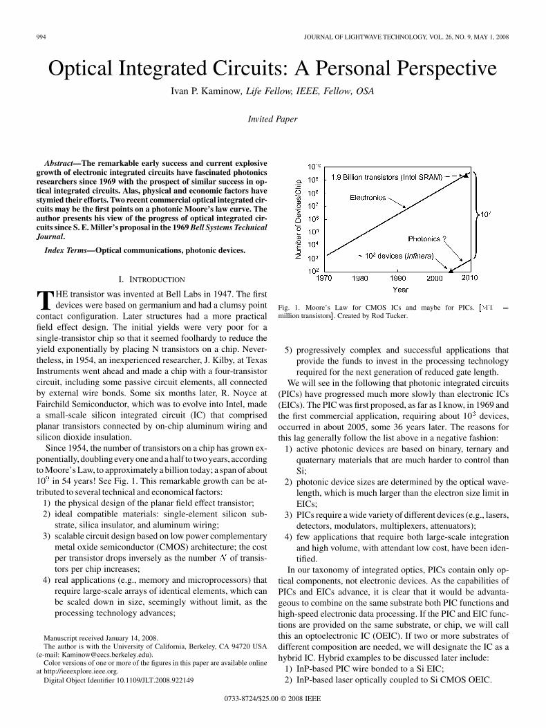
Fig. 2. 1969 BSTJ Cover and First Page of S. E. Miller article [1].
A. Disclaimer
This memoir was written with the understanding that it bebased on my personal recollections from years at Bell Labs andlater. It is not intended as a comprehensive history that acknowl-edges all the significant worldwide contributions to integratedoptics. That would be too big a job.
II. ORIGINS OF PICS AT BELL LABS
In my experience, Stewart E. Miller made the first serious pro-posal for a PIC in 1969 [1]. At the time of the first demonstrationof the laser in 1960, Stew was Director of a laboratory doing re-search on millimeter waveguide transmission systems. I was amember of his lab and was greatly influenced by his proposal.We were located at the Crawford Hill Lab of Bell Labs in ruralHolmdel, NJ. The laser was similar to a microwave source butwith shorter wavelength and offered the possibility for improvedtelecommunications. His lab therefore changed its emphasis tolaser-based telecom. By 1969, EICs had made significant com-mercial progress with more than 10 transistors per chip (seeFig. 1). It was a natural step to consider integrating some of thephotonic components in a network circuit element, such as arepeater between optical fiber transmission links that providedregeneration and routing functions, with the goal of achievingimproved performance and lower cost.
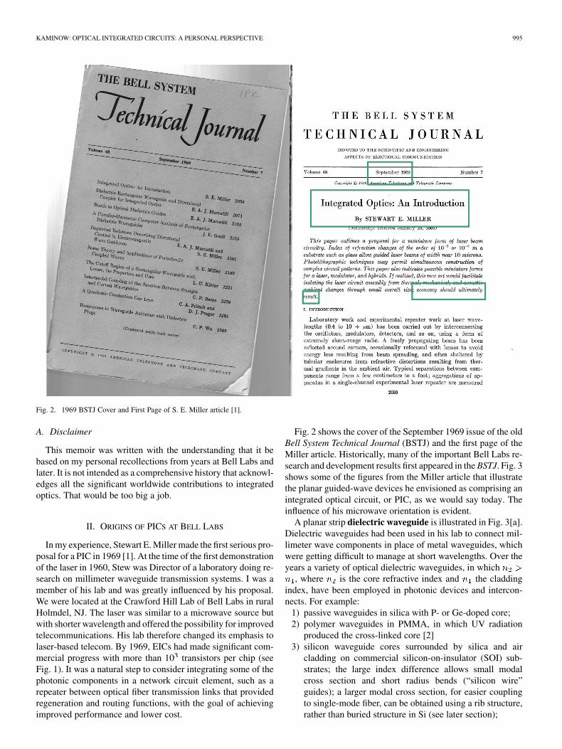
Fig. 2 shows the cover of the September 1969 issue of the oldBell System Technical Journal (BSTJ) and the first page of theMiller article. Historically, many of the important Bell Labs re-search and development results first appeared in the BSTJ. Fig. 3shows some of the figures from the Miller article that illustratethe planar guided-wave devices he envisioned as comprising anintegrated optical circuit, or PIC, as we would say today. Theinfluence of his microwave orientation is evident.
A planar strip dielectric waveguide is illustrated in Fig. 3[a].Dielectric waveguides had been used in his lab to connect mil-limeter wave components in place of metal waveguides, whichwere getting difficult to manage at short wavelengths. Over theyears a variety of optical dielectric waveguides, in which
, where is the core refractive index and the claddingindex, have been employed in photonic devices and intercon-nects. For example:
1) passive waveguides in silica with P- or Ge-doped core;2) polymer waveguides in PMMA, in which UV radiation
produced the cross-linked core [2]3) silicon waveguide cores surrounded by silica and air
cladding on commercial silicon-on-insulator (SOI) sub-strates; the large index difference allows small modalcross section and short radius bends (“silicon wire”guides); a larger modal cross section, for easier couplingto single-mode fiber, can be obtained using a rib structure,rather than buried structure in Si (see later section);
996 JOURNAL OF LIGHTWAVE TECHNOLOGY, VOL. 26, NO. 9, MAY 1, 2008
Fig. 3. Figures from 1969 BSTJ [1].
4) buried waveguides in ternary and quaternary semicon-ductor lasers and detectors, in which composition controlsindices;
5) titanium-diffused lithium niobate waveguide modulators,in which Ti diffusion defines the core [3].
Fig. 3[b] is a schematic of a proposed waveguide phase mod-ulator. It has the efficiency advantage of confining the opticaland modulating fields to the same narrow strip. The Ti-diffusedlithium niobate waveguide was invented [3] in 1974 and hasbeen employed in many commercial wideband modulators ofvarious configurations.
Fig. 3[c] illustrates a proposed planar resonator with Bragggrating mirrors that can be used as an optical filter or lasercavity. The first laser based on the Bragg resonator was demon-strated in 1971 in PMMA doped with rhodamine 6G as the gainmedium [4]. It was subsequently named a distributed Bragg re-flector (DBR) laser and has been realized in commercial semi-conductor devices. An important variant of the Bragg resonatoris the distributed feedback (DFB) resonator, which comprisesa continuous grating. The first DFB laser was demonstrated in1971 in doped dichromated gelatin [5] and, subsequently, incommercial semiconductor lasers.
The laser resonant wavelength in the DBR, a form ofFabry–Pérot resonator, is determined by the spacing, L, be-
tween gratings and the waveguide index . The roundtrip phasechange at resonance is given by
where is the phase change on reflection from a Bragggrating and is an integer. The frequency interval betweenresonances is
with the vacuum velocity of light. In order to obtain a single-longitudinal-mode laser, must be less than the gain band-width of the medium and the reflection band of the gratings.
The DFB [6], on the other hand, corresponds to a contin-uous grating with . It supports two closely spaced res-onances straddling the Bragg wavelength, , where
is the grating period. A small asymmetry in the longitudinallaser structure, such as the points of cleavage at either end, canfavor one mode, effectively yielding single-mode operation. Amore reliable method for achieving single-mode operation isto split the grating in two and introduce a quarter wave phaseshift by separating halves by . In effect, the resonator be-
KAMINOW: OPTICAL INTEGRATED CIRCUITS: A PERSONAL PERSPECTIVE 997
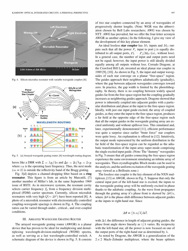
Fig. 4. Silicon microdisc resonator with variable waveguide couplers [8].
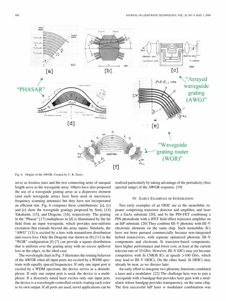
Fig. 5. [a] Arrayed waveguide grating router; [b] wavelength routing diagram.
haves like a DBR with andwhere is the operating laser frequency. Thus, the next mode
is outside the reflectivity band of the Bragg grating.Fig. 3[d] depicts a channel-dropping filter based on a ring
resonator. This figure is from an article by Marcatili, [7]another member of Miller’s lab, in the same September 1969issue of BSTJ. As in microwave systems, the resonant cavityselects carrier frequency from a frequency division multi-plexed (FDM) carrier spectrum. Currently, silicon microdiskresonators with very high have been reported [8]. Aphoto of a microdisk resonator with electrostatically controlledcoupling-waveguide spacings is shown in Fig. 4. The couplingratios can be varied through under-, critical-, and over-coupledconditions.
III. ARRAYED WAVEGUIDE GRATING ROUTER
The arrayed waveguide grating router (AWGR) is a planardevice that has proven to be ideal for multiplexing and demul-tiplexing wavelength-division-multiplexed (WDM) spectra,as well as serving as a fast wavelength-controlled switch. Aschematic diagram of the device is shown in Fig. 5. It consists
of two star couplers connected by an array of waveguides ofprogressively shorter lengths. (Note: WGR was the abbrevi-ation chosen by Bell Labs researchers; AWG was chosen byNTT. AWG has prevailed, but we offer the four-letter acronymAWGR as another option.) In the following, I give my view ofthe development of this key planar element.
An ideal lossless star coupler has inputs and out-puts such that all the power input to port j is equally dis-tributed to all output ports, (i.e., without loss).In a general case, the number of input and output ports neednot be equal; however, the input power is still ideally dividedequally among all outputs without loss. Corrado Dragone, atthe Crawford Hill Lab, invented an ideal planar star coupler in1989 [9], [10]. As shown in Fig. 5, the input and output waveg-uides of each star converge on a planar “free-space” region.The guides approach their neighbors adiabatically (gradually),where the gap between adjacent waveguides converges towardzero. In practice, the gap width is limited by the photolithog-raphy. In theory, there is no coupling between widely spacedguides far from the free-space region but the coupling graduallyincreases as neighboring guides approach. Dragone showed thatpower is inherently coupled into adjacent guides with a partic-ular distribution and phase at the input to the free-space region.Ideally, with just one input guide excited, the array of coupledguides, as they enter the input to the free-space region, producesa far field at the opposite edge of the free-space region suchthat all the output guides in the waveguide grating array are ex-cited uniformly and without spillover loss. This simulated and,later, experimentally demonstrated [11], efficient performancewas quite a surprise since earlier “brute force” star couplerswere quite lossy. An explanation is offered in [12]. Intuitively,the output mode represented by the uniform distribution in thefar field of the free-space region can be regarded as the adia-batic transformation of the input array super-mode comprisingthe single excited input guide. (Note: The “dummy” waveguidesin Fig. 5 ensure that all guides connecting the free-space regionexperience the same environment simulating an infinite array ofwaveguides. Then crystallographic Bloch modes can be used inthe analysis; and the uniform excitation of the waveguide gratingarray viewed as a Brillouin zone.)
The lossless star coupler is the key element of the NXN mul-tiplexer, [13] or AWGR, shown in Fig. 5. Suppose that only thecentral input port of the left-hand star is excited; the inputs tothe waveguide grating array will be uniformly excited in phasethanks to the adiabatic coupling. As the wave front propagatesthrough the grating array it’s phase front is skewed by ,where is the phase-shift difference between adjacent guidesat the inputs to right-hand star. Since
with the difference in length of adjacent grating guides, thephase front angle skews linearly as varies. By reciprocitywith the left-hand star, all the power is now focused on one ofthe output ports of the right-hand star as determined by .
As noted by Dragone, the AWGR is a generalization of the2 2 Mach–Zehnder multiplexer, where the beam splitters
998 JOURNAL OF LIGHTWAVE TECHNOLOGY, VOL. 26, NO. 9, MAY 1, 2008
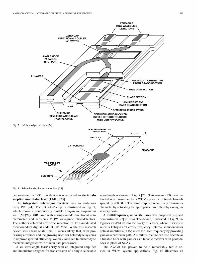
Fig. 6. Origins of the AWGR. Created by C. R. Doerr.
serve as lossless stars and the two connecting arms of unequallength serve as the waveguide array. Others have also proposedthe use of a waveguide grating array as a dispersive element(and such waveguide arrays have been used in microwavefrequency scanning antennas) but they have not incorporatedan efficient star. Fig. 6 compares these contributions: [a], [c]and [e] show the waveguide gratings proposed by Smit, [14]Takahashi, [15], and Dragone, [16], respectively. The gratingin the “Phasar” [17] multiplexer in [d] is illuminated by the farfield from an input waveguide, which provides non-uniformexcitation that extends beyond the array inputs. Similarly, the“AWG” [15] is excited by a lens with nonuniform distributionand excess loss. Only the Dragone star shown in [b] [11] in the“WGR” configuration [f] [7] can provide a square distributionthat is uniform over the grating array with no excess spilloverloss at the edges, in the ideal case.
The wavelength chart in Fig. 5 illustrates the routing behaviorof the AWGR when all input ports are excited by a WDM spec-trum with equally spaced frequencies. If only one input port isexcited by a WDM spectrum, the device serves as a demulti-plexer. If only one output port is used, the device is a multi-plexer. If a discretely tuned laser excites only one input port,the device is a wavelength-controlled switch, routing each colorto its own output. If all ports are used, novel applications can be
realized particularly by taking advantage of the periodicity (freespectral range) of the AWGR response. [19]
IV. EARLY EXAMPLES OF INTEGRATION
Two early examples of an OEIC are a) the monolithic re-peater comprising transistor detector and amplifier, and laseron a GaAs substrate [20]; and b) the PIN-FET combining aPIN photodiode with a JFET field effect transistor amplifier onan InP substrate. [20] They combine III–V photonic with III–Velectronic elements on the same chip. Such monolithic ICshave not been pursued commercially because non-integratedhybrid transceivers, with separate optimized photonic III–Vcomponents and electronic Si transistor-based components,have higher performance and lower cost, at least at the currenttelecom rate of 10 Gb/s. However, III–V EICs may yet becomecompetitive with Si CMOS ICs at speeds 100 Gb/s, whichmay lead to III–V OEICs. On the other hand, Si OEICs mayalready be near, as we discuss later.
An early effort to integrate two photonic functions combineda laser and a modulator. [22] The challenge here was to join awaveguide with a bandgap that provides laser gain with a mod-ulator whose bandgap provides transparency, on the same chip.The first successful InP laser modulator combination was
KAMINOW: OPTICAL INTEGRATED CIRCUITS: A PERSONAL PERSPECTIVE 999
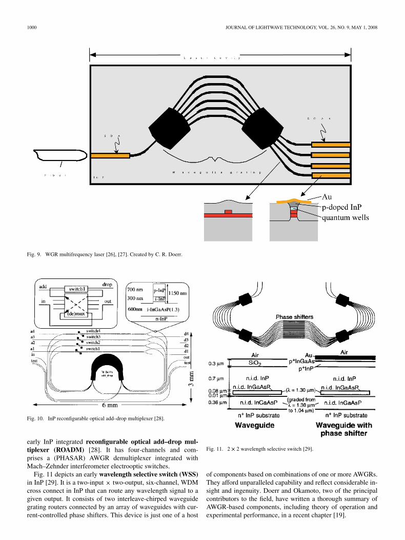
Fig. 7. InP heterodyne receiver [24].
Fig. 8. Selectable six channel transmitter [25].
demonstrated in 1987; this device is now called an electroab-sorption modulator laser (EML) [23].
The integrated heterodyne receiver was an ambitiousearly PIC [24]. The InGaAsP chip is illustrated in Fig. 7,which shows a continuously tunable 1.5- m multi-quantumwell (MQW)-DBR laser with a single-mode directional cou-pler/switch and zero-bias MQW waveguide photodetectors.The authors achieved error-free reception of FSK-modulatedpseudorandom digital code at 105 Mb/s. While this researchdevice was ahead of its time, it seems likely that, with pro-cessing advances and the growing need for heterodyne systemsto improve spectral efficiency, we may soon see InP heterodynereceivers integrated with silicon data processors.
A six-wavelength laser array with an integrated amplifierand modulator designed for transmission of a single selectable
wavelength is shown in Fig. 8 [25]. This research PIC was in-tended as a transmitter for a WDM system with fixed channelsspaced by 200 GHz. The same chip can serve many transmitterchannels, by activating the appropriate laser, thereby saving in-ventory costs.
A multifrequency, or WGR, laser was proposed [26] anddemonstrated [27] in 1994. The device, illustrated in Fig. 9, in-tegrates an AWGR into the cavity of a laser, where it serves toselect a Fabry–Pérot cavity frequency. Internal semiconductoroptical amplifiers (SOA) select the laser frequency by providinggain on a particular path. A similar structure can also operate asa tunable filter with gain or as a tunable receiver with photodi-odes in place of SOAs.
The AWGR has proven to be a remarkably fertile de-vice in WDM system applications. Fig. 10 illustrates an
1000 JOURNAL OF LIGHTWAVE TECHNOLOGY, VOL. 26, NO. 9, MAY 1, 2008
Fig. 9. WGR multifrequency laser [26], [27]. Created by C. R. Doerr.
Fig. 10. InP reconfigurable optical add–drop multiplexer [28].
early InP integrated reconfigurable optical add–drop mul-tiplexer (ROADM) [28]. It has four-channels and com-prises a (PHASAR) AWGR demultiplexer integrated withMach–Zehnder interferometer electrooptic switches.
Fig. 11 depicts an early wavelength selective switch (WSS)in InP [29]. It is a two-input two-output, six-channel, WDMcross connect in InP that can route any wavelength signal to agiven output. It consists of two interleave-chirped waveguidegrating routers connected by an array of waveguides with cur-rent-controlled phase shifters. This device is just one of a host
Fig. 11. 2� 2 wavelength selective switch [29].
of components based on combinations of one or more AWGRs.They afford unparalleled capability and reflect considerable in-sight and ingenuity. Doerr and Okamoto, two of the principalcontributors to the field, have written a thorough summary ofAWGR-based components, including theory of operation andexperimental performance, in a recent chapter [19].
KAMINOW: OPTICAL INTEGRATED CIRCUITS: A PERSONAL PERSPECTIVE 1001
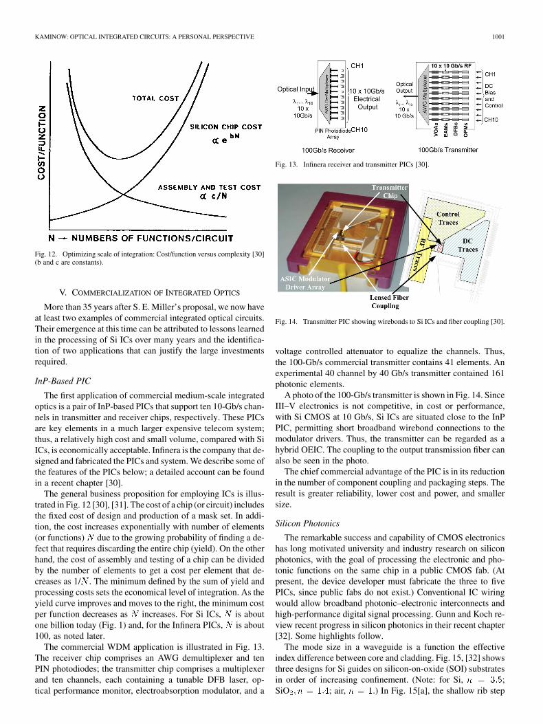
Fig. 12. Optimizing scale of integration: Cost/function versus complexity [30](b and c are constants).
V. COMMERCIALIZATION OF INTEGRATED OPTICS
More than 35 years after S. E. Miller’s proposal, we now haveat least two examples of commercial integrated optical circuits.Their emergence at this time can be attributed to lessons learnedin the processing of Si ICs over many years and the identifica-tion of two applications that can justify the large investmentsrequired.
InP-Based PIC
The first application of commercial medium-scale integratedoptics is a pair of InP-based PICs that support ten 10-Gb/s chan-nels in transmitter and receiver chips, respectively. These PICsare key elements in a much larger expensive telecom system;thus, a relatively high cost and small volume, compared with SiICs, is economically acceptable. Infinera is the company that de-signed and fabricated the PICs and system. We describe some ofthe features of the PICs below; a detailed account can be foundin a recent chapter [30].
The general business proposition for employing ICs is illus-trated in Fig. 12 [30], [31]. The cost of a chip (or circuit) includesthe fixed cost of design and production of a mask set. In addi-tion, the cost increases exponentially with number of elements(or functions) due to the growing probability of finding a de-fect that requires discarding the entire chip (yield). On the otherhand, the cost of assembly and testing of a chip can be dividedby the number of elements to get a cost per element that de-creases as 1/ . The minimum defined by the sum of yield andprocessing costs sets the economical level of integration. As theyield curve improves and moves to the right, the minimum costper function decreases as increases. For Si ICs, is aboutone billion today (Fig. 1) and, for the Infinera PICs, is about100, as noted later.
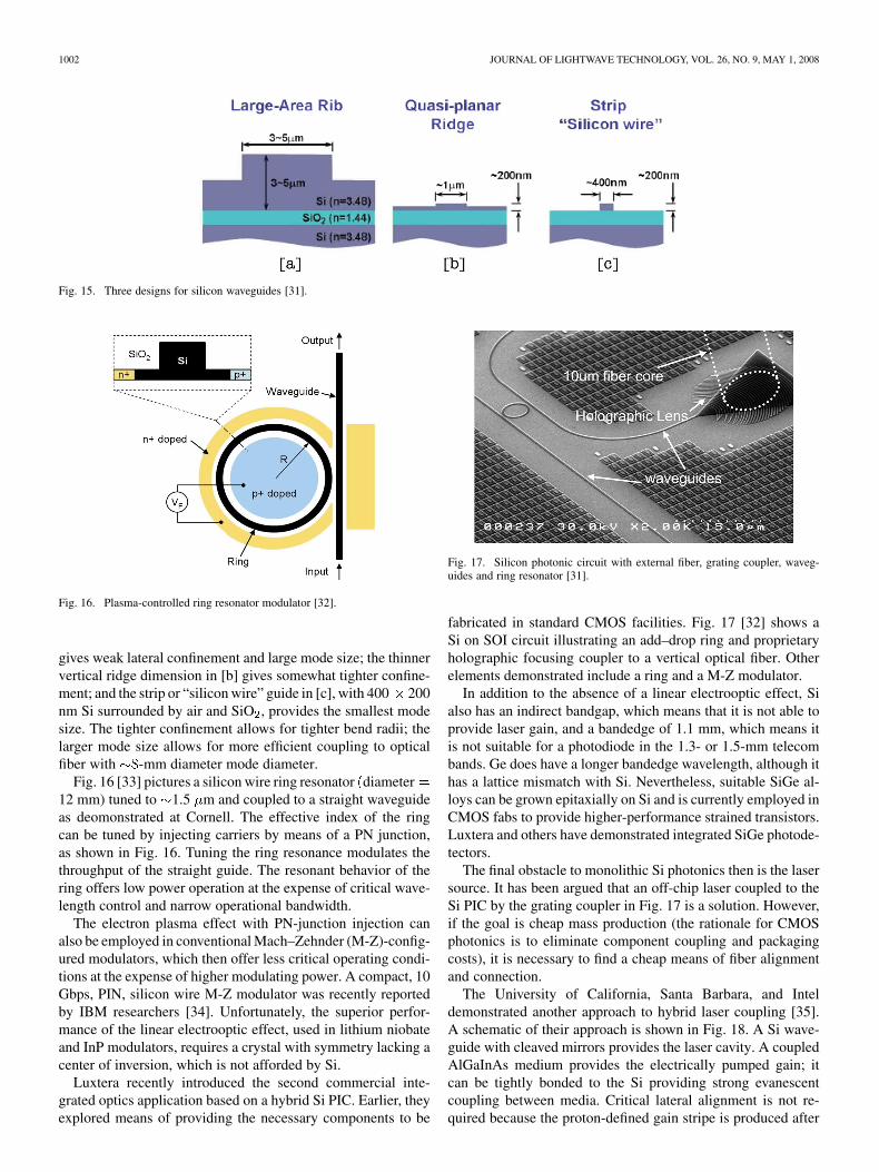
The commercial WDM application is illustrated in Fig. 13.The receiver chip comprises an AWG demultiplexer and tenPIN photodiodes; the transmitter chip comprises a multiplexerand ten channels, each containing a tunable DFB laser, op-tical performance monitor, electroabsorption modulator, and a
Fig. 13. Infinera receiver and transmitter PICs [30].
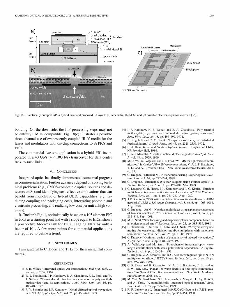
Fig. 14. Transmitter PIC showing wirebonds to Si ICs and fiber coupling [30].
voltage controlled attenuator to equalize the channels. Thus,the 100-Gb/s commercial transmitter contains 41 elements. Anexperimental 40 channel by 40 Gb/s transmitter contained 161photonic elements.
A photo of the 100-Gb/s transmitter is shown in Fig. 14. SinceIII–V electronics is not competitive, in cost or performance,with Si CMOS at 10 Gb/s, Si ICs are situated close to the InPPIC, permitting short broadband wirebond connections to themodulator drivers. Thus, the transmitter can be regarded as ahybrid OEIC. The coupling to the output transmission fiber canalso be seen in the photo.
The chief commercial advantage of the PIC is in its reductionin the number of component coupling and packaging steps. Theresult is greater reliability, lower cost and power, and smallersize.
Silicon Photonics
The remarkable success and capability of CMOS electronicshas long motivated university and industry research on siliconphotonics, with the goal of processing the electronic and pho-tonic functions on the same chip in a public CMOS fab. (Atpresent, the device developer must fabricate the three to fivePICs, since public fabs do not exist.) Conventional IC wiringwould allow broadband photonic–electronic interconnects andhigh-performance digital signal processing. Gunn and Koch re-view recent progress in silicon photonics in their recent chapter[32]. Some highlights follow.
The mode size in a waveguide is a function the effectiveindex difference between core and cladding. Fig. 15, [32] showsthree designs for Si guides on silicon-on-oxide (SOI) substratesin order of increasing confinement. (Note: for Si, ;SiO ; air, .) In Fig. 15[a], the shallow rib step
1002 JOURNAL OF LIGHTWAVE TECHNOLOGY, VOL. 26, NO. 9, MAY 1, 2008
Fig. 15. Three designs for silicon waveguides [31].
Fig. 16. Plasma-controlled ring resonator modulator [32].
gives weak lateral confinement and large mode size; the thinnervertical ridge dimension in [b] gives somewhat tighter confine-ment; and the strip or “silicon wire” guide in [c], with 400 200nm Si surrounded by air and SiO , provides the smallest modesize. The tighter confinement allows for tighter bend radii; thelarger mode size allows for more efficient coupling to opticalfiber with -mm diameter mode diameter.
Fig. 16 [33] pictures a silicon wire ring resonator diameter12 mm) tuned to 1.5 m and coupled to a straight waveguideas deomonstrated at Cornell. The effective index of the ringcan be tuned by injecting carriers by means of a PN junction,as shown in Fig. 16. Tuning the ring resonance modulates thethroughput of the straight guide. The resonant behavior of thering offers low power operation at the expense of critical wave-length control and narrow operational bandwidth.
The electron plasma effect with PN-junction injection canalso be employed in conventional Mach–Zehnder (M-Z)-config-ured modulators, which then offer less critical operating condi-tions at the expense of higher modulating power. A compact, 10Gbps, PIN, silicon wire M-Z modulator was recently reportedby IBM researchers [34]. Unfortunately, the superior perfor-mance of the linear electrooptic effect, used in lithium niobateand InP modulators, requires a crystal with symmetry lacking acenter of inversion, which is not afforded by Si.
Luxtera recently introduced the second commercial inte-grated optics application based on a hybrid Si PIC. Earlier, theyexplored means of providing the necessary components to be
Fig. 17. Silicon photonic circuit with external fiber, grating coupler, waveg-uides and ring resonator [31].
fabricated in standard CMOS facilities. Fig. 17 [32] shows aSi on SOI circuit illustrating an add–drop ring and proprietaryholographic focusing coupler to a vertical optical fiber. Otherelements demonstrated include a ring and a M-Z modulator.
In addition to the absence of a linear electrooptic effect, Sialso has an indirect bandgap, which means that it is not able toprovide laser gain, and a bandedge of 1.1 mm, which means itis not suitable for a photodiode in the 1.3- or 1.5-mm telecombands. Ge does have a longer bandedge wavelength, although ithas a lattice mismatch with Si. Nevertheless, suitable SiGe al-loys can be grown epitaxially on Si and is currently employed inCMOS fabs to provide higher-performance strained transistors.Luxtera and others have demonstrated integrated SiGe photode-tectors.
The final obstacle to monolithic Si photonics then is the lasersource. It has been argued that an off-chip laser coupled to theSi PIC by the grating coupler in Fig. 17 is a solution. However,if the goal is cheap mass production (the rationale for CMOSphotonics is to eliminate component coupling and packagingcosts), it is necessary to find a cheap means of fiber alignmentand connection.
The University of California, Santa Barbara, and Inteldemonstrated another approach to hybrid laser coupling [35].A schematic of their approach is shown in Fig. 18. A Si wave-guide with cleaved mirrors provides the laser cavity. A coupledAlGaInAs medium provides the electrically pumped gain; itcan be tightly bonded to the Si providing strong evanescentcoupling between media. Critical lateral alignment is not re-quired because the proton-defined gain stripe is produced after
KAMINOW: OPTICAL INTEGRATED CIRCUITS: A PERSONAL PERSPECTIVE 1003
Fig. 18. Electrically pumped InP/Si hybrid laser and proposed IC layout: (a) schematic, (b) SEM, and (c) possible electronic-photonic circuit [33].
bonding. On the downside, the InP processing steps may notbe entirely CMOS compatible. Fig. 18(c) illustrates a possiblethree-channel use of evanescently coupled III–V media for thelasers and modulators with on-chip connections to Si PICs andEICs.
The commercial Luxtera application is a hybrid PIC incor-porated in a 40 Gb/s (4 10G b/s) transceiver for data centerrack-to-rack links.
VI. CONCLUSION
Integrated optics has finally demonstrated some real progressin commercialization. Further advances depend on solving tech-nical problems (e.g., CMOS-compatible optical sources and de-tectors on Si) and identifying cost-effective applications that canbenefit from monolithic or hybrid OEIC capabilities (e.g., re-ducing coupling and packaging costs, integrating photonic andelectronic processing, and realizing low cost per unit at high vol-umes).
R. Tucker’s Fig. 1, optimistically based on a 10 element PICin 2005 as a starting point and with a slope equal to EICs, showsa prospective Moore’s law for PICs, 1agging EICs by only afactor of 10 . A few more points for commercial applicationsare required to define a trend.
ACKNOWLEDGMENT
I am grateful to C. Doerr and T. Li for their insightful com-ments.
REFERENCES
[1] S. E. Miller, “Integrated optics: An introduction,” Bell Syst. Tech. J.,vol. 48, p. 2059, 1969.
[2] W. J. Tomlinson, I. P. Kaminow, E. A. Chandross, R. L. Fork, and W.T. Silfvast, “Photoinduced refractive index increase in poly (methyl-methacrylate) and its applications,” Appl. Phys. Lett., vol. 16, pp.486–489, 1970.
[3] R. V. Schmidt and I. P. Kaminow, “Metal-diffused optical waveguidesin LiNbO3,” Appl. Phys. Lett., vol. 25, pp. 458–460, 1974.
[4] I. P. Kaminow, H. P. Weber, and E. A. Chandross, “Poly (methylmethacrylate) dye laser with internal diffraction grating resonator,”Appl. Phys. Lett., vol. 18, pp. 497–499, 1971.
[5] H. Kogelnik and C. V. Shank, “Coupled-wave theory of distributedfeedback lasers,” J. Appl. Phys., vol. 43, pp. 2328–2335, 1972.
[6] H. A. Haus, Waves and Fields in Optoelectronics. Englewood Cliffs,NJ: Prentice-Hall, 1984.
[7] E. A. J. Marcatili, “Bends in optical dielectric guides,” Bell Syst. Tech.J., vol. 48, p. 2059, 1969.
[8] M. C. Wu, O. Solgaard, and J. E. Ford, “MEMS for lightwave commu-nication,” in Optical Fiber Telecommunications, V. A, I. P. Kaminow,T. Li, and A. E. Willner, Eds. New York: Academic/Elsevier, 2008,ch. 19.
[9] C. Dragone, “Efficient N�N star couplers using Fourier optics,” Elec-tron. Lett., vol. 24, pp. 242–244, 1988.
[10] C. Dragone, “Efficient N�N star couplers using Fourier optics,” J.Lightw. Technol., vol. 7, no. 3, pp. 479–489, Mar. 1989.
[11] C. Dragone, C. H. Henry, I. P. Kaminow, and R. C. Kistler, “Efficientmultichannel integrated optics star coupler on silicon,” IEEE Phototon.Technol. Lett., vol. 1, no. 8, pp. 241–243, Aug. 1989.
[12] I. P. Kaminow, “FSK with direct detection in optical multi-access FDMnetworks,” IEEE J. Sel. Areas Commun., vol. 8, no. 6, pp. 1005–1014,Aug. 1990.
[13] C. Dragone, “An N�N optical multiplexer using a planar arrangementof two star couplers,” IEEE Photon. Technol. Lett., vol. 3, no. 9, pp.812–814, Sep. 1991.
[14] M. K. Smit, “New focussing and dispersive planar component based onan optical phased array,” Electron. Lett., vol. 24, pp. 385–386, 1988.
[15] H. Takahashi, S. Suzuki, K. Kato, and I. Nishi, “Arrayed-waveguidegrating for wavelength division multi/demultiplexer with nanometerresolution,” Electron. Lett., vol. 26, pp. 87–88, 1990.
[16] C. Dragone, “Optimum design of planar array of tapered waveguides,”J. Opt. Soc. Amer. A, pp. 2081–2093, 1991.
[17] A. Vellekoop and M. Smit, “Four-channel integrated-optic wave-length demultiplexer with weak polarization dependence,” J. Lightw.Technol., vol. 9, pp. 310–314, 1991.
[18] C. Dragone, C. A. Edwards, and R. C. Kistler, “Integrated optics N�Nmultiplexer on silicon,” IEEE Photon. Technol. Lett., vol. 3, no. 10, pp.896–899, Oct. 1991.
[19] C. R. Doerr and K. Okamoto, , V. A, I. P. Kaminow, T. Li, and A.E. Willner, Eds., “Planar lightwave circuits in fiber-optic communica-tions,” in Optical Fiber Telecommunications. New York: AcademicPress/Elsevier, 2008, ch. 9.
[20] M. Yust, N. Bar-Chaim, S. H. Izadpanah, S. Margalit, I. Ury, D. Wilt,and A. Yariv, “A monolithically integrated optical repeater,” Appl.Phys. Lett., vol. 35, pp. 795–796, 1979.
[21] R. F. Leheny et al., “Integrated In/0.53/Ga/0.47/As p-i-n F.E.T. pho-toreceiver,” Electron. Lett., vol. 16, pp. 353–354, 1980.
1004 JOURNAL OF LIGHTWAVE TECHNOLOGY, VOL. 26, NO. 9, MAY 1, 2008
[22] L. A. Coldren, B. I. Miller, K. Iga, and J. A. Rentschler, “Monolithictwo-section gainasp/inp active-optical-resonator devices formed by re-active ion etching,” Appl. Phys. Lett., vol. 38, pp. 315–317, 1981.
[23] M. Suzuki, “Monolithic integration of InGaAsp/InP distributed feed-back laser and electroabsorption modulator by vapor phase epitaxy,” J.Lightw. Technol., vol. 5, no. 9, pp. 1277–1285, Sep. 1987.
[24] T. L. Koch et al., “GaInAs/GaInAsP multiple-quantum-well integratedheterodyne receiver,” Electron. Lett., vol. 25, pp. 1621–1623, 1989.
[25] M. G. Young et al., “Six wavelength laser array with integrated ampli-fier and modulator,” Electron. Lett., vol. 31, pp. 1835–1836, 1995.
[26] B. Glance, I. P. Kaminow, and R. W. Wilson, “Applications of theintegrated waveguide grating router,” J. Lightw. Technol., vol. 12, no.6, pp. 957–962, Jun. 1994.
[27] M. Zirngibl, B. Glance, L. W. Stulz, C. H. Joyner, G. Raybon, and I. P.Kaminow, “Characterization of a multiwavelength waveguide gratingrouter laser,” IEEE Photon. Technol. Lett., vol. 6, no. 9, pp. 1082–1084,Sep. 1994.
[28] C. G. M. Vreeburg et al., “First InP-based reconfigurable integratedadd-drop multiplexer,” IEEE Photon. Technol. Lett., vol. 9, no. 2, pp.188–190, Feb. 1997.
[29] C. R. Doerr, C. H. Joyner, L. W. Stulz, and R. Monnard, “Wavelength-division multiplexing cross connect in InP,” IEEE Photon. Technol.Lett., vol. 10, no. 1, pp. 117–119, jan. 1998.
[30] C. Joyner, D. Lambert, P. Evans, and M. Raburn, , V. A, I. P. Kaminow,T. Li, and A. E. Willner, Eds., “III-V Photonic integrated circuitsand their impact on optical network architectures,” in Optical FiberTelecommunications. New York: Academic/Elsevier, 2008, ch. 10.
[31] R. N. Noyce, “Large-scale integration: What is yet to come?,” Science,vol. 195, pp. 102–1106, 1977.
[32] C. Gunn and T. L. Koch, , V. A, I. P. Kaminow, T. Li, and A. E.Willner, Eds., “Silicon photonics,” in Optical Fiber Telecommunica-tions. : Academic/Elsevier, 2008, ch. 11.
[33] Q. Xu, B. Schmidt, S. Pradhan, and M. Lipson, “Micrometre-scale sil-icon electro-optic modulator,” Nature, vol. 435, pp. 325–327, 2005.
[34] W. M. J. Green, M. J. Rooks, L. Sekaric, and Y. A. Vlasosov, “Ultra-compact, low rf power, 10 Gb/s silicon mach-zehnder modulator,” Opt.Express, vol. 15, pp. 17106–17113, 2007.
[35] A. W. Fang, H. Park, O. Cohen, R. Jones, M. J. Paniccia, and J. E.Bowers, “Electrically pumped hybrid AlGaInAs-silicon evanescentlaser,” Opt. Express, vol. 14, pp. 9203–9210, 2006.
Ivan P. Kaminow (LF’95) received the B.S.E.E.degree from Union College, Schenectady, NY, theM.S.E. degree from the University of California, LosAngeles (UCLA), and the A.M. and Ph.D. degreesfrom Harvard University. He was a Hughes Fellowat UCLA and a Bell Labs Fellow at Harvard. retiredfrom Bell Laboratories, Holmdel, NJ, in 1996 aftera 42-year career (1954–1996), mostly in lightwaveresearch. At Bell Laboratories, he did seminalstudies on electrooptic modulators and materials,Raman scattering in ferroelectrics, integrated optics
(including titanium-diffused lithium niobate modulators), semiconductor lasers(including the DBR laser, ridge waveguide InGaAsP laser, and multifrequencylaser), birefringent optical fibers, and WDM lightwave networks. Later, asHead of the Photonic Networks and Components Research Department, heled research on WDM components (including the erbium-doped fiber ampli-fier, waveguide grating router, and the fiber Fabry–Pérot resonator), and onWDM local and wide area networks. Earlier (1952–1954), he did research onmicrowave antenna arrays at Hughes Aircraft Company. After retiring fromBell Laboratories, he served as IEEE Congressional Fellow on the staffs of theHouse Science Committee and the Congressional Research Service (SciencePolicy Research Division) in the Library of Congress. From 1997 to 1999,he returned to Lucent Bell Laboratories as a part-time Consultant. He alsoestablished Kaminow Lightwave Technology to provide consulting servicesto technology companies and to patent and litigation law firms. In 1999, heserved as Senior Science Advisor to the Optical Society of America. He hasbeen Visiting Professor at Princeton, Berkeley, Columbia, the University ofTokyo, and Kwangju University (Korea). Currently, he is Adjunct Professor inElectrical Engineering and Computer Science at the University of California,Berkeley, where he has been teaching since 2004. He has published over240 papers, received 47 patents, and has written or coedited six books, themost recent being Optical Fiber Telecommunications V A & B (AcademicPress/Elsevier, 2008), co-edited with T. Li and A. Willner and published inFebruary 2008.
Dr. Kaminow is a Fellow of the American Physical Society and the OpticalSociety of America (OSA). He is a member of the National Academy of Engi-neering, a Diplomate of the American Board of Laser Surgery, and a Fellow ofthe New York Academy of Medicine. He is the recipient of the Bell Labs Dis-tinguished Member of Technical Staff Award, the IEEE Quantum ElectronicsAward, the OSA Charles Townes Award, the IEEE/LEOS/OSA John TyndallAward, and the IEEE Third Millennium Medal and Union College Alumni GoldMedal.