Embed Size (px)
Citation preview
Keysight TechnologiesMXG X-Series Signal Generators N5181B Analog & N5182B Vector
9 kHz to 3 or 6 GHz
Data Sheet
Definitions and Conditions
Specifications represent warranted performance of a calibrated instrument that has been stored for a minimum of 2 hours within the operating temperature range of 0 to 55 °C, unless otherwise stated, and after a 45 minute warm-up period. The specifications include measurement uncertainty. Data represented in this document are specifications unless otherwise noted.
Typical (typ) describes additional product performance information that is not covered by the product warranty. It is performance beyond specifications that 80 percent of the units exhibit with a 90 percent confidence level at room temperature (approximately 25 °C). Typical performance does not include measurement uncertainty.
Nominal (nom) values indicate the expected mean or average performance, or an attribute whose performance is by design, such as the 50 ohm connector. This data is not warranted and is measured at room temperature (approximately 25 °C).
Measured (meas) describes an attribute measured during the design phase for purposes of communicating expected performance, such as amplitude drift vs. time. This data is not warranted and is measured at room temperature (approximately 25 °C).
Table of Contents Pure and preciseOn the path to better performance, the Keysight Technologies, Inc. MXG X-Series signal generators are fine-tuned to be your “golden transmitter” in R&D. Whether you’re pushing for a linear RF chain or an optimized link budget, the analog and vector MXG models deliver what you need: phase noise, ACPR, channel coding, and more. Take your devices and designs to the limit with the MXG.
Definitions and conditions ....................................................................................................... 2Frequency specifications ......................................................................................................... 3Amplitude specifications ......................................................................................................... 5Spectral purity specifications ............................................................................................... 10Analog modulation specifications ......................................................................................... 13Vector modulation specifications—N5182B only ................................................................. 18General specifications ........................................................................................................... 29Inputs and outputs ................................................................................................................. 30Related literature ................................................................................................................... 32
02 | Keysight | MXG X-Series Signal Generators N5181B Analog & N5182B Vector - Data Sheet
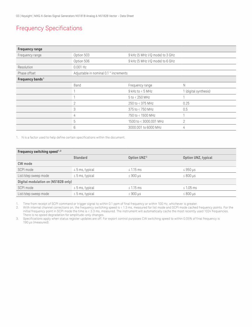
Frequency Specifications
Frequency range
Frequency range Option 503 9 kHz (5 MHz I/Q mode) to 3 GHz
Option 506 9 kHz (5 MHz I/Q mode) to 6 GHz
Resolution 0.001 Hz
Phase offset Adjustable in nominal 0.1 ° increments
Frequency bands 1
Band Frequency range N
1 9 kHz to < 5 MHz 1 (digital synthesis)
1 5 to < 250 MHz 1
2 250 to < 375 MHz 0.25
3 375 to < 750 MHz 0.5
4 750 to < 1500 MHz 1
5 1500 to < 3000.001 MHz 2
6 3000.001 to 6000 MHz 4
1. N is a factor used to help define certain specifications within the document.
Frequency switching speed 1, 2
Standard Option UNZ 3 Option UNZ, typical
CW mode
SCPI mode ≤ 5 ms, typical ≤ 1.15 ms ≤ 950 µs
List/step sweep mode ≤ 5 ms, typical ≤ 900 µs ≤ 800 µs
Digital modulation on (N5182B only)
SCPI mode ≤ 5 ms, typical ≤ 1.15 ms ≤ 1.05 ms
List/step sweep mode ≤ 5 ms, typical ≤ 900 µs ≤ 800 µs
1. Time from receipt of SCPI command or trigger signal to within 0.1 ppm of final frequency or within 100 Hz, whichever is greater.2. With internal channel corrections on, the frequency switching speed is < 1.3 ms, measured for list mode and SCPI mode cached frequency points. For the
initial frequency point in SCPI mode the time is < 3.3 ms, measured. The instrument will automatically cache the most recently used 1024 frequencies. There is no speed degradation for amplitude-only changes.
3. Specifications apply when status register updates are off. For export control purposes CW switching speed to within 0.05% of final frequency is 190 μs (measured).
03 | Keysight | MXG X-Series Signal Generators N5181B Analog & N5182B Vector - Data Sheet
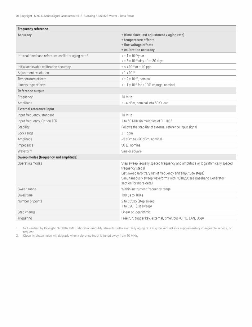
Frequency reference
Accuracy ± (time since last adjustment x aging rate)± temperature effects ± line voltage effects± calibration accuracy
Internal time base reference oscillator aging rate 1 < ± 1 x 10⁻⁷/year< ± 5 x 10⁻¹⁰/day after 30 days
Initial achievable calibration accuracy ± 4 x 10⁻⁸ or ± 40 ppb
Adjustment resolution < 1 x 10⁻¹⁰
Temperature effects < ± 2 x 10⁻¹⁰, nominal
Line voltage effects < ± 1 x 10⁻⁹ for ± 10% change, nominal
Reference output
Frequency 10 MHz
Amplitude ≥ +4 dBm, nominal into 50 Ω load
External reference input
Input frequency, standard 10 MHz
Input frequency, Option 1ER 1 to 50 MHz (in multiples of 0.1 Hz) 2
Stability Follows the stability of external reference input signal
Lock range ± 1 ppm
Amplitude –3 dBm to +20 dBm, nominal
Impedance 50 Ω, nominal
Waveform Sine or square
Sweep modes (frequency and amplitude)
Operating modes Step sweep (equally spaced frequency and amplitude or logarithmically spaced frequency steps)List sweep (arbitrary list of frequency and amplitude steps)Simultaneously sweep waveforms with N5182B; see Baseband Generator section for more detail
Sweep range Within instrument frequency range
Dwell time 100 µs to 100 s
Number of points 2 to 65535 (step sweep)1 to 3201 (list sweep)
Step change Linear or logarithmic
Triggering Free run, trigger key, external, timer, bus (GPIB, LAN, USB)
1. Not verified by Keysight N7800A TME Calibration and Adjustments Software. Daily aging rate may be verified as a supplementary chargeable service, on request.
2. Close-in phase noise will degrade when reference input is tuned away from 10 MHz.
04 | Keysight | MXG X-Series Signal Generators N5181B Analog & N5182B Vector - Data Sheet
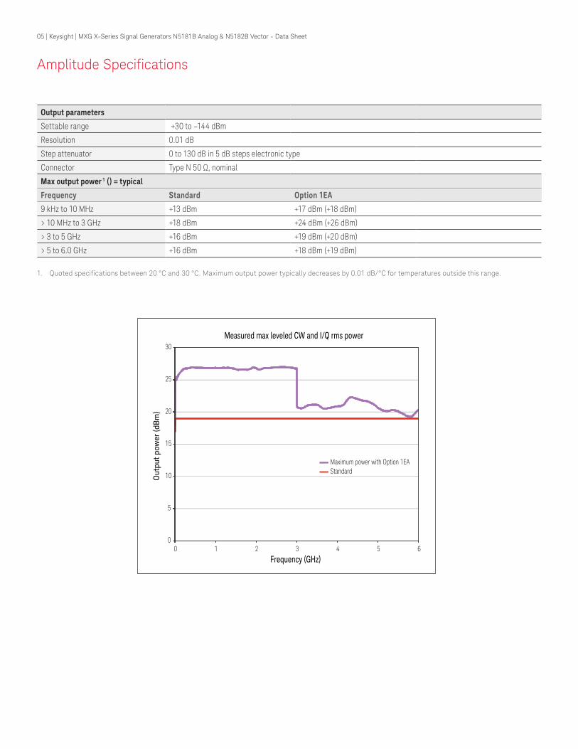
Output parameters
Settable range +30 to –144 dBm
Resolution 0.01 dB
Step attenuator 0 to 130 dB in 5 dB steps electronic type
Connector Type N 50 Ω, nominal
Max output power 1 () = typical
Frequency Standard Option 1EA
9 kHz to 10 MHz +13 dBm +17 dBm (+18 dBm)
> 10 MHz to 3 GHz +18 dBm +24 dBm (+26 dBm)
> 3 to 5 GHz +16 dBm +19 dBm (+20 dBm)
> 5 to 6.0 GHz +16 dBm +18 dBm (+19 dBm)
1. Quoted specifications between 20 °C and 30 °C. Maximum output power typically decreases by 0.01 dB/°C for temperatures outside this range.
Amplitude Specifications
0
5
10
15
20
25
30
0 1 2 3 4 5 6
Out
put p
ower
(dB
m)
Frequency (GHz)
Measured max leveled CW and I/Q rms power
Maximum power with Option 1EAStandard
05 | Keysight | MXG X-Series Signal Generators N5181B Analog & N5182B Vector - Data Sheet
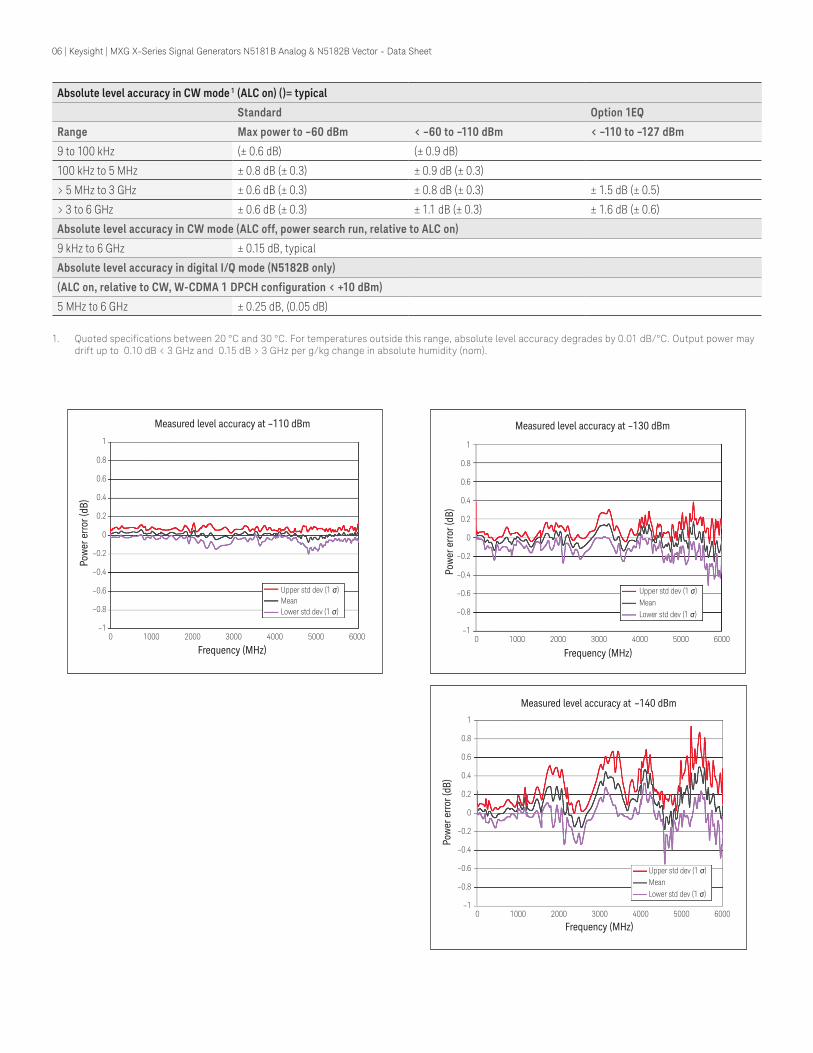
Absolute level accuracy in CW mode 1 (ALC on) ()= typical
Standard Option 1EQ
Range Max power to –60 dBm < –60 to –110 dBm < –110 to –127 dBm
9 to 100 kHz (± 0.6 dB) (± 0.9 dB)
100 kHz to 5 MHz ± 0.8 dB (± 0.3) ± 0.9 dB (± 0.3)
> 5 MHz to 3 GHz ± 0.6 dB (± 0.3) ± 0.8 dB (± 0.3) ± 1.5 dB (± 0.5)
> 3 to 6 GHz ± 0.6 dB (± 0.3) ± 1.1 dB (± 0.3) ± 1.6 dB (± 0.6)
Absolute level accuracy in CW mode (ALC off, power search run, relative to ALC on)
9 kHz to 6 GHz ± 0.15 dB, typical
Absolute level accuracy in digital I/Q mode (N5182B only)
(ALC on, relative to CW, W-CDMA 1 DPCH configuration < +10 dBm)
5 MHz to 6 GHz ± 0.25 dB, (0.05 dB)
1. Quoted specifications between 20 °C and 30 °C. For temperatures outside this range, absolute level accuracy degrades by 0.01 dB/°C. Output power may drift up to 0.10 dB < 3 GHz and 0.15 dB > 3 GHz per g/kg change in absolute humidity (nom).
Measured level accuracy at –140 dBm
Frequency (MHz)
Pow
er e
rror
(dB)
1
0.8
0.6
0.4
0.2
0
–0.2
–0.4
–0.6
–0.8
–10 1000 2000 3000 4000 5000 6000
Upper std dev (1 σ)MeanLower std dev (1 σ)
Measured level accuracy at –110 dBm
Frequency (MHz)
Pow
er e
rror
(dB)
1
0.8
0.6
0.4
0.2
0
–0.2
–0.4
–0.6
–0.8
–1
Upper std dev (1 σ)MeanLower std dev (1 σ)
0 1000 2000 3000 4000 5000 6000
Measured level accuracy at –130 dBm
Frequency (MHz)
Pow
er e
rror
(dB)
1
0.8
0.6
0.4
0.2
0
–0.2
–0.4
–0.6
–0.8
–1
Upper std dev (1 σ)MeanLower std dev (1 σ)
0 1000 2000 3000 4000 5000 6000
06 | Keysight | MXG X-Series Signal Generators N5181B Analog & N5182B Vector - Data Sheet
0 20 40 60 80 100 120
0.5
0.4
0.3
0.2
0.1
0
–0.1
–0.2
–0.3
–0.4
–0.5
Elapsed time (minutes)
Delta
from
initi
al (d
B)
Measured amplitude repeatablity +5 dBm ALC on
850 MHz
1900 MHz
2200 MHz
3500 MHz
5800 MHz
Measured relative level accuracy at 850 MHz initial power +10 dBm
Final power (dBm)
Pow
er e
rror
(dB)
0 –20 –40 -60 –80 –100 –120 –140
0.5
0.4
0.3
0.2
0.1
0
–0.1
–0.2
–0.3
–0.4
–0.5
Upper std dev (1 σ)MeanLower std dev (1 σ)
Measured ALC linearity1900 MHz, CW, relative to 0 dBm
Amplitude (dB)–20 –15 –10 –5 0 5 10
0.3
0.2
0.1
0
–0.1
–0.2
–0.3
Erro
r (dB
)
Upper std dev (1 σ)MeanLower std dev (1 σ )
Measured ALC linearity850 MHz, CW, relative to 0 dBm
Amplitude (dB)
–20 –15 –10 –5 0 5 10
0.3
0.2
0.1
0
–0.1
–0.2
–0.3
Erro
r (dB
)
Upper std dev (1 σ)MeanLower std dev (1 σ)
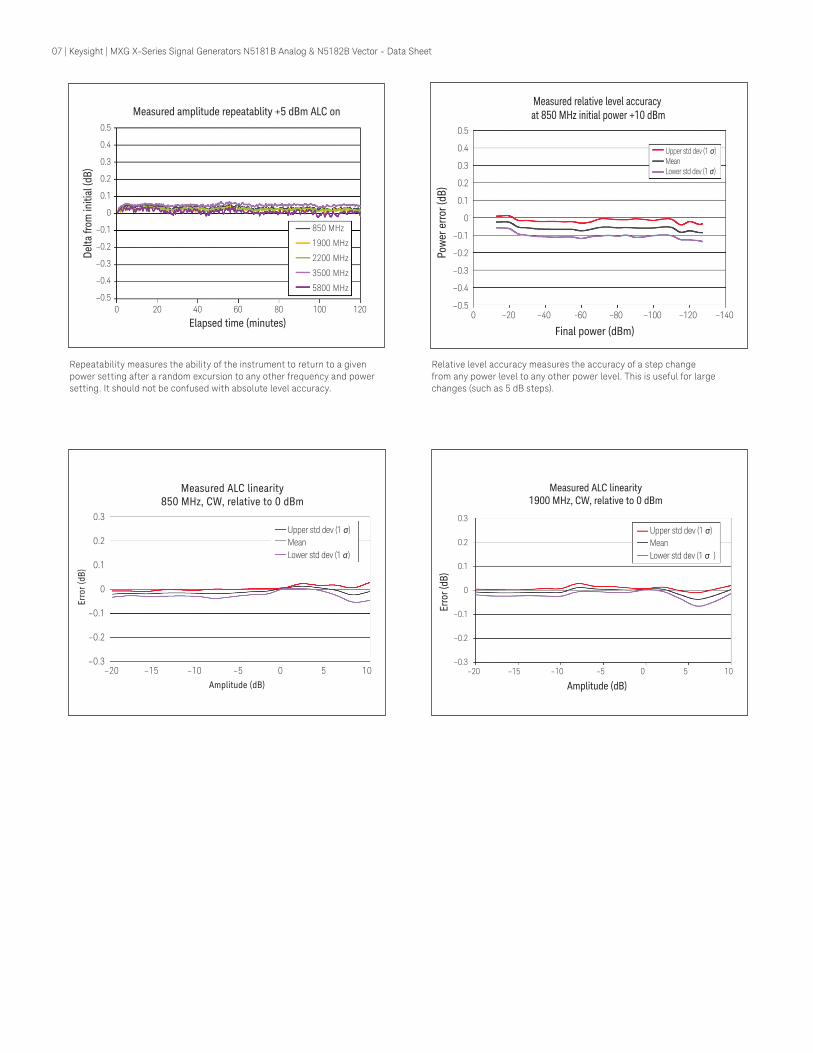
Relative level accuracy measures the accuracy of a step change from any power level to any other power level. This is useful for large changes (such as 5 dB steps).
Repeatability measures the ability of the instrument to return to a given power setting after a random excursion to any other frequency and power setting. It should not be confused with absolute level accuracy.
07 | Keysight | MXG X-Series Signal Generators N5181B Analog & N5182B Vector - Data Sheet
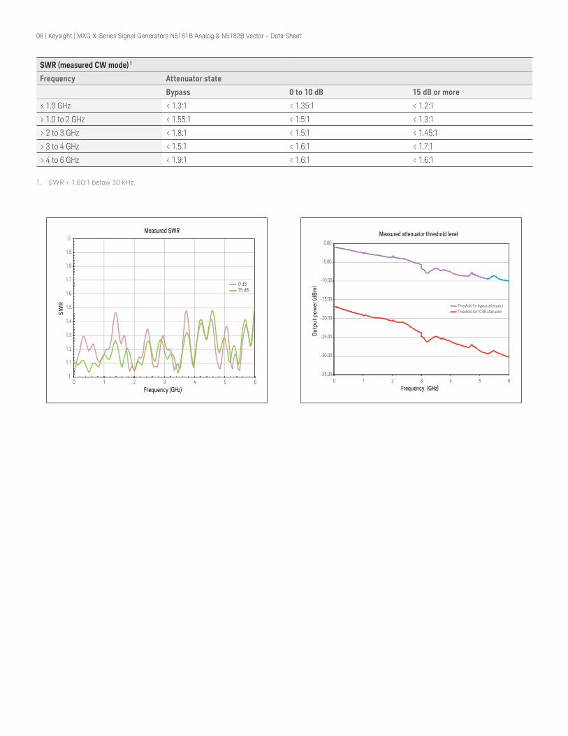
SWR (measured CW mode) 1
Frequency Attenuator state
Bypass 0 to 10 dB 15 dB or more
≤ 1.0 GHz < 1.3:1 < 1.35:1 < 1.2:1
> 1.0 to 2 GHz < 1.55:1 < 1:5:1 < 1.3:1
> 2 to 3 GHz < 1.8:1 < 1.5:1 < 1.45:1
> 3 to 4 GHz < 1.5:1 < 1.6:1 < 1.7:1
> 4 to 6 GHz < 1.9:1 < 1.6:1 < 1.6:1
1. SWR < 1.60:1 below 30 kHz.
1
1.1
1.2
1.3
1.4
1.5
1.6
1.7
1.8
1.9
2
0 1 2 3 4 5 6
SW
R
Frequency (GHz)
Measured SWR
0 dB 15 dB
-35.00
-30.00
-25.00
-20.00
-15.00
-10.00
-5.00
0.00
0 1 2 3 4 5 6
Out
put p
ower
(dB
m)
Frequency (GHz)
Measured attenuator threshold level
Threshold for bypass attenuatorThreshold for 10 dB attenuator
08 | Keysight | MXG X-Series Signal Generators N5181B Analog & N5182B Vector - Data Sheet
Maximum reverse power, nominal
< 1 GHz 50 W
> 1 to 2 GHz 25 W
> 2 to 6 GHz 20 W
Max DC voltage 50 VDC
Trip level 2 W
Amplitude switching speed 1 Standard Option UNZ Option UNZ, typical
CW mode
SCPI mode ≤ 5 ms, typical ≤ 750 µs ≤ 650 µs
Power search SCPI mode < 12 ms, measured
List/step sweep mode ≤ 5 ms, typical ≤ 500 µs ≤ 300 µs
Digital modulation on (N5182B only)
SCPI mode ≤ 5 ms, typical ≤ 1.15 ms ≤ 950 µs
Power search SCPI mode < 12 ms, measured
List/step sweep mode ≤ 5 ms, typical ≤ 900 µs ≤ 400 µs
Alternate power level control (N5182B only)
Switching time(via waveform markers)
20 µs within ± 1 dB, measured
Functional power range –15 dBm to –144 dBm, measured
User flatness correction
Number of points 3201
Number of tables Dependent on available free memory in instrument; 10,000 maximum
Entry modes USB/LAN direct power meter control, LAN to GPIB and USB to GPIB, remote bus and manual USB/GPIB power meter control
Sweep modes
See Frequency Specifications section for more detail
1. Time from receipt of SCPI command or trigger signal to amplitude settled within 0.2 dB. Switching speed specifications apply when status register updates are off.
09 | Keysight | MXG X-Series Signal Generators N5181B Analog & N5182B Vector - Data Sheet
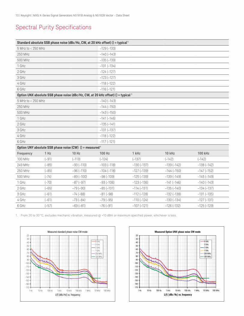
Standard absolute SSB phase noise (dBc/Hz, CW, at 20 kHz offset) () = typical 1
5 MHz to < 250 MHz –129 (–133)
250 MHz –140 (–143)
500 MHz –135 (–139)
1 GHz –131 (–134)
2 GHz –124 (–127)
3 GHz –123 (–127)
4 GHz –118 (–122)
6 GHz –116 (–121)
Option UNX absolute SSB phase noise (dBc/Hz, CW, at 20 kHz offset) () = typical 1
5 MHz to < 250 MHz –140 (–143)
250 MHz –144 (–150)
500 MHz –143 (–150)
1 GHz –141 (–146)
2 GHz –135 (–141)
3 GHz –131 (–137)
4 GHz –118 (–122)
6 GHz –117 (–121)
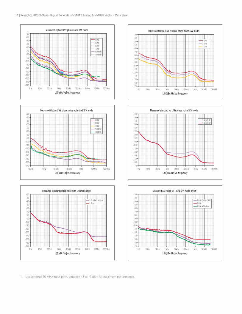
Option UNY absolute SSB phase noise (CW) () = measured 1
Frequency 1 Hz 10 Hz 100 Hz 1 kHz 10 kHz 100 kHz
100 MHz (–91) (–113) (–124) (–137) (–142) (–142)
249 MHz (–85) –93 (–110) –103 (–118) –130 (–137) –139 (–142) –138 (–142)
250 MHz (–85) –96 (–110) –104 (–118) –127 (–139) –144 (–150) –147 (–152)
500 MHz (–74) –89 (–100) –98 (–109) –125 (–139) –139 (–149) –145 (–149)
1 GHz (–70) –87 (–97) –93 (–106) –123 (–136) –141 (–146) –140 (–143)
2 GHz (–65) –79 (–90) –85 (–101) –114 (–131) –135 (–140) –134 (–137)
3 GHz (–61) –74 (–88) –81 (–98) –112 (–128) –132 (–138) –131 (–135)
4 GHz (–61) –73 (–84) –79 (–95) –110 (–124) –130 (–134) –127 (–131)
6 GHz (–57) –69 (–81) –76 (–91) –107 (–121) –126 (-132) –125 (–129)
1. From 20 to 30 °C, excludes mechanic vibration, measured @ +10 dBm or maximum specified power, whichever is less.
Spectral Purity Specifications
-170
-160
-150
-140
-130
-120
-110
-100
-90
-80
-70
-60
-50
-40
-30
-20
Measured standard phase noise CW mode
1 Hz 10 Hz 100 Hz 1 kHz 10 kHz 100 kHz 1 MHz, 10 MHz 100 MHz
L(f) [dBc/Hz] vs. frequency
6 GHz3 GHz2 GHz1 GHz250 MHz100 MHz
- 170- 160- 150- 140- 130- 120- 110- 100- 90- 80- 70- 60- 50- 40- 30- 20
Measured Option UNX phase noise CW mode
1 Hz 10 Hz 100 Hz 1 kHz 10 kHz 100 kHz 1 MHz, 10 MHz 100 MHz
L(f) [dBc/Hz] vs. frequency
6 GHz3 GHz2 GHz1 GHz250 MHz100 MHz
10 | Keysight | MXG X-Series Signal Generators N5181B Analog & N5182B Vector - Data Sheet
-170
-160
-150
-140
-130
-120
-110
-100
-90
-80
-70
-60
-50
-40
-30
-20
Measured Option UNY phase noise CW mode
1 Hz 10 Hz 100 Hz 1 kHz 10 kHz 100 kHz 1 MHz, 10 MHz 100 MHz
L(f) [dBc/Hz] vs. frequency
6 GHz3 GHz2 GHz1 GHz250 MHz100 MHz
-170
-160
-150
-140
-130
-120
-110
-100
-90
-80
-70
-60
-50
-40
-30
-20
Measured standard phase noise with I/Q modulation
1 Hz 10 Hz 100 Hz 1 kHz 10 kHz 100 kHz 1 MHz, 10 MHz 100 MHz
L(f) [dBc/Hz] vs. frequency
1 GHz DIG mod on1 GHz
-170
-160
-150
-140
-130
-120
-110
-100
-90
-80
-70
-60
-50
-40
-30
-20
Measured Option UNY phase noise optimized S/N mode
100 Hz 1 kHz 10 kHz 100 kHz 1 MHz 10 MHz 100 MHz
L(f) [dBc/Hz] vs. frequency
6 GHz3 GHz1 GHz250 MHz100 MHz
-170
-160
-150
-140
-130
-120
-110
-100
-90
-80
-70
-60
-50
-40
-30
-20
Measured Option UNY residual phase noise CW mode 1
1 Hz 10 Hz 100 Hz 1 kHz 10 kHz 100 kHz 1 MHz, 10 MHz 100 MHz
L(f) [dBc/Hz] vs. frequency
6 GHz3 GHz1 GHz
-170
-160
-150
-140
-130
-120
-110
-100
-90
-80
-70
-60
-50
-40
-30
-20
Measured AM noise @ 1 GHz S/N mode on/off
1 Hz 10 Hz 100 Hz 1 kHz 10 kHz 100 kHz 1 MHz, 10 MHz 100 MHz
L(f) [dBc/Hz] vs. frequency
1 GHz 0 dBm SNR1 GHz1 GHz +23 dBm
-170
-160
-150
-140
-130
-120
-110
-100
-90
-80
-70
-60
-50
-40
-30
-20
Measured standard vs. UNY phase noise S/N mode
1 Hz 10 Hz 100 Hz 1 kHz 10 kHz 100 kHz 1 MHz, 10 MHz 100 MHz
L(f) [dBc/Hz] vs. frequency
1 GHz STD1 GHz UNY
1. Use external 10 MHz input path, between +3 to +7 dBm for maximum performance.
11 | Keysight | MXG X-Series Signal Generators N5181B Analog & N5182B Vector - Data Sheet
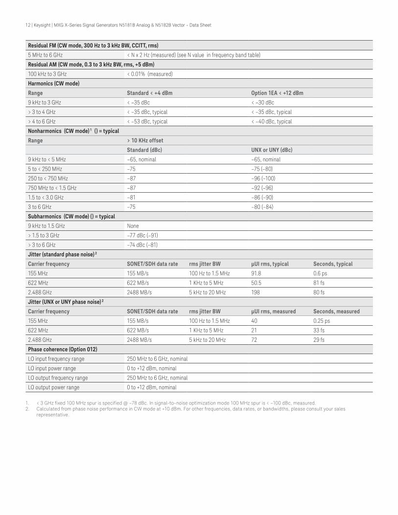
Residual FM (CW mode, 300 Hz to 3 kHz BW, CCITT, rms)
5 MHz to 6 GHz < N x 2 Hz (measured) (see N value in frequency band table)
Residual AM (CW mode, 0.3 to 3 kHz BW, rms, +5 dBm)
100 kHz to 3 GHz < 0.01% (measured)
Harmonics (CW mode)
Range Standard < +4 dBm Option 1EA < +12 dBm
9 kHz to 3 GHz < –35 dBc < –30 dBc
> 3 to 4 GHz < –35 dBc, typical < –35 dBc, typical
> 4 to 6 GHz < –53 dBc, typical < –40 dBc, typical
Nonharmonics (CW mode) 1 () = typical
Range > 10 KHz offset
Standard (dBc) UNX or UNY (dBc)
9 kHz to < 5 MHz –65, nominal –65, nominal
5 to < 250 MHz –75 –75 (–80)
250 to < 750 MHz –87 –96 (–100)
750 MHz to < 1.5 GHz –87 –92 (–96)
1.5 to < 3.0 GHz –81 –86 (–90)
3 to 6 GHz –75 –80 (–84)
Subharmonics (CW mode) () = typical
9 kHz to 1.5 GHz None
> 1.5 to 3 GHz –77 dBc (–91)
> 3 to 6 GHz –74 dBc (–81)
Jitter (standard phase noise) 2
Carrier frequency SONET/SDH data rate rms jitter BW μUI rms, typical Seconds, typical
155 MHz 155 MB/s 100 Hz to 1.5 MHz 91.8 0.6 ps
622 MHz 622 MB/s 1 KHz to 5 MHz 50.5 81 fs
2.488 GHz 2488 MB/s 5 kHz to 20 MHz 198 80 fs
Jitter (UNX or UNY phase noise) 2
Carrier frequency SONET/SDH data rate rms jitter BW μUI rms, measured Seconds, measured
155 MHz 155 MB/s 100 Hz to 1.5 MHz 40 0.25 ps
622 MHz 622 MB/s 1 KHz to 5 MHz 21 33 fs
2.488 GHz 2488 MB/s 5 kHz to 20 MHz 72 29 fs
Phase coherence (Option 012)
LO input frequency range 250 MHz to 6 GHz, nominal
LO input power range 0 to +12 dBm, nominal
LO output frequency range 250 MHz to 6 GHz, nominal
LO output power range 0 to +12 dBm, nominal
1. < 3 GHz fixed 100 MHz spur is specified @ –78 dBc. In signal-to-noise optimization mode 100 MHz spur is < –100 dBc, measured.2. Calculated from phase noise performance in CW mode at +10 dBm. For other frequencies, data rates, or bandwidths, please consult your sales
representative.
12 | Keysight | MXG X-Series Signal Generators N5181B Analog & N5182B Vector - Data Sheet
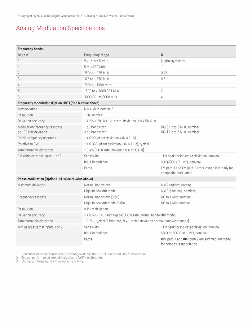
Analog Modulation Specifications
Frequency bands
Band # Frequency range N
1 9 kHz to < 5 MHz (digital synthesis)
1 5 to < 250 MHz 1
2 250 to < 375 MHz 0.25
3 375 to < 750 MHz 0.5
4 750 to < 1500 MHz 1
5 1500 to < 3000.001 MHz 2
6 3000.001 to 6000 MHz 4
Frequency modulation (Option UNT) (See N value above)
Max deviation N × 4 MHz, nominal 3
Resolution 1 Hz, nominal
Deviation accuracy < ± 2% + 20 Hz (1 kHz rate, deviation is N x 50 kHz)
Modulation frequency response @ 100 kHz deviation
1 dB bandwidth3 dB bandwidth
DC/5 Hz to 3 MHz, nominalDC/1 Hz to 7 MHz, nominal
Carrier frequency accuracy < ± 0.2% of set deviation + (N × 1 Hz) 1
Relative to CW < ± 0.06% of set deviation + (N × 1 Hz), typical 2
Total harmonic distortion < 0.4% [1 kHz rate, deviation is N x 50 kHz]
FM using external inputs 1 or 2 Sensitivity +1 V peak for indicated deviation, nominal
Input impedance 50 Ω/600 Ω/1 MΩ, nominal
Paths FM path 1 and FM path 2 are summed internally for composite modulation
Phase modulation (Option UNT) (See N value above)
Maximum deviation Normal bandwidth N × 2 radians, nominal
High-bandwidth mode N × 0.2 radians, nominal
Frequency response Normal bandwidth (3 dB) DC to 1 MHz, nominal
High-bandwidth mode (3 dB) DC to 4 MHz, nominal
Resolution 0.1% of deviation
Deviation accuracy < + 0.5% + 0.01 rad, typical [1 kHz rate, normal bandwidth mode]
Total harmonic distortion < 0.2%, typical [1 kHz rate, N x 1 radian deviation normal bandwidth mode]
ΦM using external inputs 1 or 2 Sensitivity +1 V peak for indicated deviation, nominal
Input impedance 50 Ω or 600 Ω or 1 MΩ, nominal
Paths ΦM path 1 and ΦM path 2 are summed internally for composite modulation
1. Specification valid for temperature changes of less than ± 5 °C since last DCFM calibration.2. Typical performance immediately after a DCFM calibration.3. Digital synthesis band FM deviation is 5 MHz.
13 | Keysight | MXG X-Series Signal Generators N5181B Analog & N5182B Vector - Data Sheet
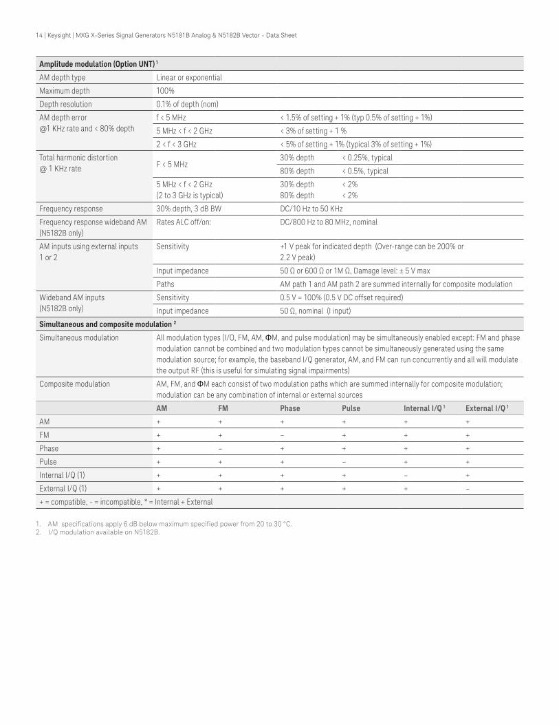
Amplitude modulation (Option UNT) 1
AM depth type Linear or exponential
Maximum depth 100%
Depth resolution 0.1% of depth (nom)
AM depth error @1 KHz rate and < 80% depth
f < 5 MHz < 1.5% of setting + 1% (typ 0.5% of setting + 1%)
5 MHz < f < 2 GHz < 3% of setting + 1 %
2 < f < 3 GHz < 5% of setting + 1% (typical 3% of setting + 1%)
Total harmonic distortion @ 1 KHz rate F < 5 MHz
30% depth < 0.25%, typical
80% depth < 0.5%, typical
5 MHz < f < 2 GHz (2 to 3 GHz is typical)
30% depth80% depth
< 2%< 2%
Frequency response 30% depth, 3 dB BW DC/10 Hz to 50 KHz
Frequency response wideband AM (N5182B only)
Rates ALC off/on: DC/800 Hz to 80 MHz, nominal
AM inputs using external inputs 1 or 2
Sensitivity +1 V peak for indicated depth (Over-range can be 200% or 2.2 V peak)
Input impedance 50 Ω or 600 Ω or 1M Ω, Damage level: ± 5 V max
Paths AM path 1 and AM path 2 are summed internally for composite modulation
Wideband AM inputs (N5182B only)
Sensitivity 0.5 V = 100% (0.5 V DC offset required)
Input impedance 50 Ω, nominal (I input)
Simultaneous and composite modulation 2
Simultaneous modulation All modulation types (I/O, FM, AM, ΦM, and pulse modulation) may be simultaneously enabled except: FM and phase modulation cannot be combined and two modulation types cannot be simultaneously generated using the same modulation source; for example, the baseband I/Q generator, AM, and FM can run concurrently and all will modulate the output RF (this is useful for simulating signal impairments)
Composite modulation AM, FM, and ΦM each consist of two modulation paths which are summed internally for composite modulation; modulation can be any combination of internal or external sources
AM FM Phase Pulse Internal I/Q 1 External I/Q 1
AM + + + + + +
FM + + – + + +
Phase + – + + + +
Pulse + + + – + +
Internal I/Q (1) + + + + – +
External I/Q (1) + + + + + –
+ = compatible, - = incompatible, * = Internal + External
1. AM specifications apply 6 dB below maximum specified power from 20 to 30 °C.2. I/Q modulation available on N5182B.
14 | Keysight | MXG X-Series Signal Generators N5181B Analog & N5182B Vector - Data Sheet
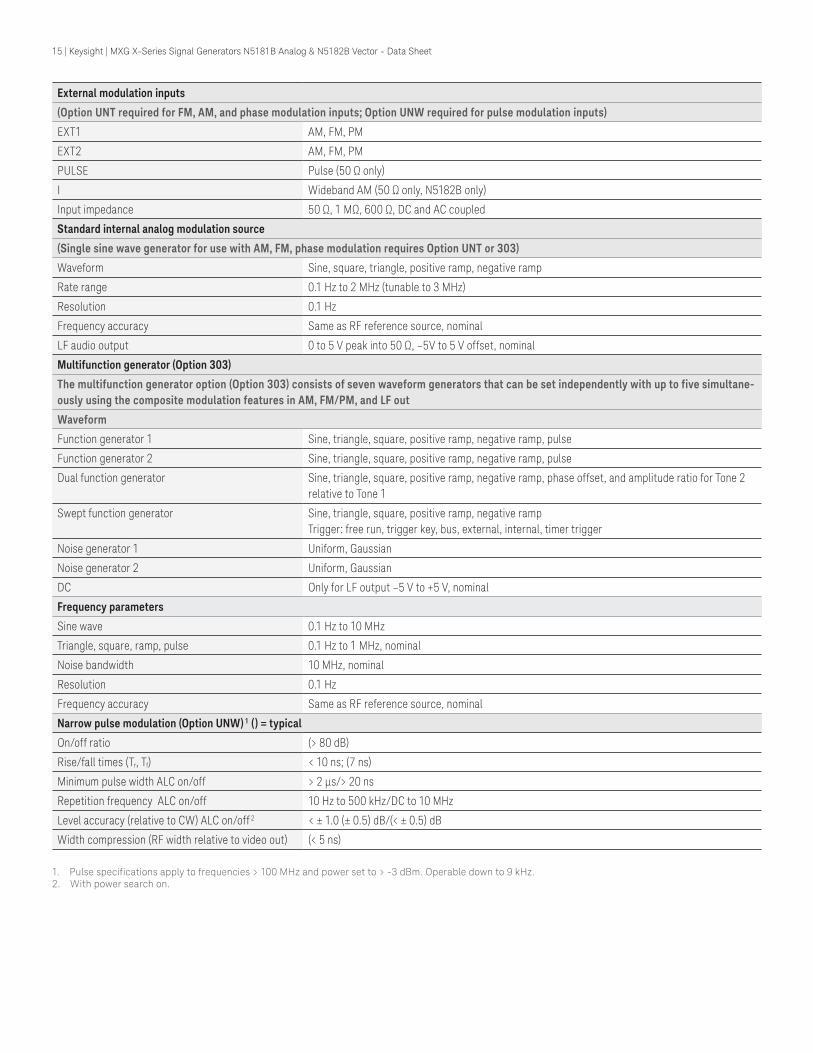
External modulation inputs
(Option UNT required for FM, AM, and phase modulation inputs; Option UNW required for pulse modulation inputs)
EXT1 AM, FM, PM
EXT2 AM, FM, PM
PULSE Pulse (50 Ω only)
I Wideband AM (50 Ω only, N5182B only)
Input impedance 50 Ω, 1 MΩ, 600 Ω, DC and AC coupled
Standard internal analog modulation source
(Single sine wave generator for use with AM, FM, phase modulation requires Option UNT or 303)
Waveform Sine, square, triangle, positive ramp, negative ramp
Rate range 0.1 Hz to 2 MHz (tunable to 3 MHz)
Resolution 0.1 Hz
Frequency accuracy Same as RF reference source, nominal
LF audio output 0 to 5 V peak into 50 Ω, –5V to 5 V offset, nominal
Multifunction generator (Option 303)
The multifunction generator option (Option 303) consists of seven waveform generators that can be set independently with up to five simultane-ously using the composite modulation features in AM, FM/PM, and LF out
Waveform
Function generator 1 Sine, triangle, square, positive ramp, negative ramp, pulse
Function generator 2 Sine, triangle, square, positive ramp, negative ramp, pulse
Dual function generator Sine, triangle, square, positive ramp, negative ramp, phase offset, and amplitude ratio for Tone 2 relative to Tone 1
Swept function generator Sine, triangle, square, positive ramp, negative rampTrigger: free run, trigger key, bus, external, internal, timer trigger
Noise generator 1 Uniform, Gaussian
Noise generator 2 Uniform, Gaussian
DC Only for LF output –5 V to +5 V, nominal
Frequency parameters
Sine wave 0.1 Hz to 10 MHz
Triangle, square, ramp, pulse 0.1 Hz to 1 MHz, nominal
Noise bandwidth 10 MHz, nominal
Resolution 0.1 Hz
Frequency accuracy Same as RF reference source, nominal
Narrow pulse modulation (Option UNW) 1 () = typical
On/off ratio (> 80 dB)
Rise/fall times (Tr, Tf) < 10 ns; (7 ns)
Minimum pulse width ALC on/off > 2 µs/> 20 ns
Repetition frequency ALC on/off 10 Hz to 500 kHz/DC to 10 MHz
Level accuracy (relative to CW) ALC on/off 2 < ± 1.0 (± 0.5) dB/(< ± 0.5) dB
Width compression (RF width relative to video out) (< 5 ns)
1. Pulse specifications apply to frequencies > 100 MHz and power set to > -3 dBm. Operable down to 9 kHz.2. With power search on.
15 | Keysight | MXG X-Series Signal Generators N5181B Analog & N5182B Vector - Data Sheet
Video feed-through 1 ≤ 3GHz/> 3 GHz (< 50 mV/< 5mV )
External video delay (ext input to video) 30 ns, nominal
RF delay (video to RF output) 20 ns, nominal
Pulse overshoot (< 15%)
Input level +1 Vpeak = RF on into 50 Ω, nominal
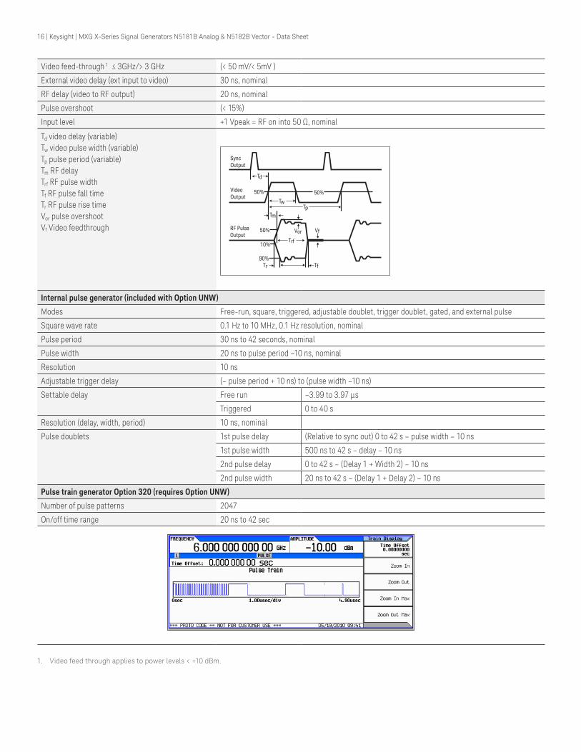
Td video delay (variable)Tw video pulse width (variable) Tp pulse period (variable)Tm RF delayTrf RF pulse width Tf RF pulse fall time Tr RF pulse rise time Vor pulse overshoot Vf Video feedthrough
SyncOutput
VideoOutput
RF PulseOutput
Td
Tm
Tw
Trf
Vf
TfTr
Vor
Tp
50%
50%
10%
90%
50%
Internal pulse generator (included with Option UNW)
Modes Free-run, square, triggered, adjustable doublet, trigger doublet, gated, and external pulse
Square wave rate 0.1 Hz to 10 MHz, 0.1 Hz resolution, nominal
Pulse period 30 ns to 42 seconds, nominal
Pulse width 20 ns to pulse period –10 ns, nominal
Resolution 10 ns
Adjustable trigger delay (– pulse period + 10 ns) to (pulse width –10 ns)
Settable delay Free run –3.99 to 3.97 µs
Triggered 0 to 40 s
Resolution (delay, width, period) 10 ns, nominal
Pulse doublets 1st pulse delay (Relative to sync out) 0 to 42 s – pulse width – 10 ns
1st pulse width 500 ns to 42 s – delay – 10 ns
2nd pulse delay 0 to 42 s – (Delay 1 + Width 2) – 10 ns
2nd pulse width 20 ns to 42 s – (Delay 1 + Delay 2) – 10 ns
Pulse train generator Option 320 (requires Option UNW)
Number of pulse patterns 2047
On/off time range 20 ns to 42 sec
1. Video feed through applies to power levels < +10 dBm.
16 | Keysight | MXG X-Series Signal Generators N5181B Analog & N5182B Vector - Data Sheet
Avionics (Option 302)
VOR
Bearing accuracy ± 0.1 degrees
Frequency accuracy Same as RF reference source, nominal
AM accuracy 30% depth ± 5% of setting
AM distortion 2%
FM accuracy 480 Hz deviation ± 1.7 Hz
ILS: localizer and glide slope
AM accuracy 40% depth ± 5% of setting
AM distortion 2%
Difference in depth of modulation (DDM) resolution
Localizer 0.0002
Glide slope 0.0004
Difference in depth of modulation (DDM) accuracy
Localizer ± 0.0004 ± 5% of DDM1
Glide slope ± 0.0008 ± 5% of DDM1
Marker beacon
Marker tone AM accuracy 95% depth ± 5% of setting + 1%
Marker tone AM distortion 95% depth 5%
1. DDM must not be equal to 0.
17 | Keysight | MXG X-Series Signal Generators N5181B Analog & N5182B Vector - Data Sheet
Vector Modulation Specifications
N5182B only
I/Q modulator external inputs 1
Bandwidth Baseband (I or Q)RF (I+Q)
Up to 100 MHz baseband, nominalUp to 200 MHz RF, nominal
I or Q offset ± 100 mV (200 uV resolution)
I/Q gain balance ± 4 dB (0.001 dB resolution)
I/Q attenuation 0 to 50 dB (0.01 dB resolution)
Quadrature angle adjustment ± 200 units (0.1 units resolution)
Full scale input drive (I+Q) 0.5 V into 50 Ω, nominal
Internal I/Q baseband generator adjustments 1, 2 (Options 656 and 657)
I/Q offset ± 20% (0.025% resolution)
I/Q gain ± 1 dB (0.001 dB resolution)
Quadrature angle adjustment ± 10 ° (0.01 degrees resolution)
I/Q phase ± 360.00 ° (0.01 degrees resolution)
I/Q skew ± 800.00 ns (1 picosecond resolution)
I/Q delay ± 250.00 ns (1 picosecond resolution)
External I/Q outputs 1
Impedance 50 Ω, nominal per output
100 Ω, nominal differential output
Type Single-ended or differential (Option 1EL)
Maximum voltage per output 1 V peak-to-peak or 0.5 V peak
Bandwidth (I, Q) Baseband (I or Q) 80 MHz, nominal (Option 656 and 657)
RF (I+Q) 160 MHz, nominal (Option 656 and 657)
Amplitude flatness ± 0.2 dB measured with channel corrections optimized for I/Q output
Phase flatness ± 2.5 degrees measured with channel corrections optimized for I/Q output
Common mode I/Q offset ± 1.5 V into 50 Ω (200 µV resolution)
Differential mode I or Q offset ± 50 mV into 50 Ω (200 µV resolution)
1. I/Q adjustments represent user intverface nominal parameter ranges and not specifications.2. Internal I/Q adjustments apply to RF out and I/Q outputs simultaneously.
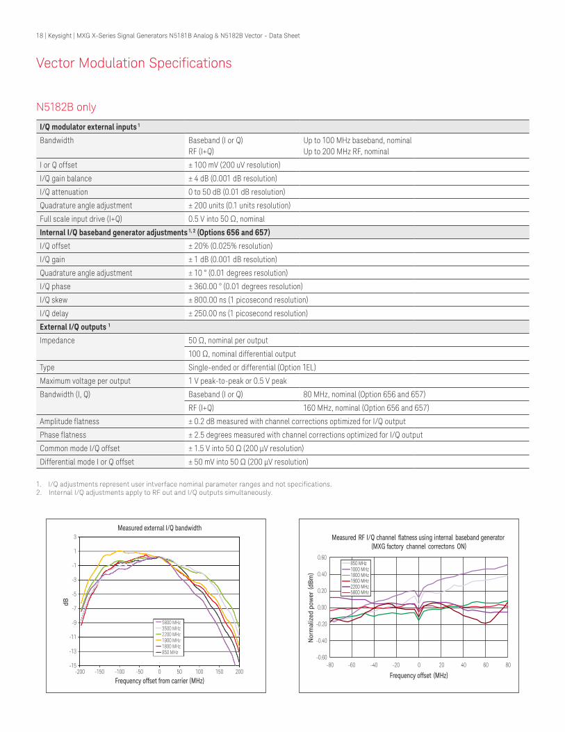
-200 -150 -100 -50 0 50 100 150 200
3
1
-1
-3
-5
-7
-9
-11
-13
-15
Frequency offset from carrier (MHz)
Measured external I/Q bandwidth
dB
5800 MHz3500 MHz2200 MHz1900 MHz1800 MHz850 MHz
-80 -60 -40 0-20 20 40 60 80
Nor
mal
ized
pow
er (
dBm
)
Frequency offset (MHz)
Measured RF I/Q channel flatness using internal baseband generator (MXG factory channel correctons ON)
-0.60
-0.40
-0.20
0.00
0.20
0.40
0.60850 MHz1000 MHz1800 MHz1900 MHz2200 MHz5800 MHz
18 | Keysight | MXG X-Series Signal Generators N5181B Analog & N5182B Vector - Data Sheet

Internal real-time complex digital I/Q filters (included with Option 656)
Factory channel correction (256 taps)
Corrects the linear phase and amplitude response of the baseband I/Q and RF outputs of the signal generator using factory calibration arrays. (default mode is off)
RF amplitude flatness (160 MHz) ± 0.2 dB measured
RF phase flatness (160 MHz) ± 2 degrees measured
User channel correction (256 taps)
Automated routine uses power sensor to correct for linear phase and amplitude response of DUT (equalizer). See Users Guide for more details.
Recommended max amplitude error for correction
± 15 dB
Recommended max phase error for correction
± 25 degrees
Equalization filter (256 taps)
User can download and apply inverse or custom phase and amplitude response coefficients from tools such as MATLAB, 89600 VSA or SystemVue to correct for linear errors of DUT/system. See Users Guide for more details.
Baseband generator (Options 656 and 657)
Channels 2 [I and Q]
Resolution 16 bits [1/65,536]
Sample rate Option 656Option 656 and 657
100 Sa/s to 100 MSa/s100 Sa/s to 200 MSa/s
Maximum number of waveform files in cache 1024
RF (I+Q) bandwidth Option 656Option 656 and 657
80 MHz, nominal160 MHz, nominal
Interpolated DAC rate 800 MHz (waveforms only need OSR = 1.25 )
Frequency offset range ± 80 MHz
Digital sweep modes In list sweep mode each point in the list can have independent waveforms (N5182B) along with user definable frequencies and amplitudes; see the Amplitude and Frequency Specifications sections for more detail.
Waveform switching speed 1
SCPI mode≤ 5 ms, measured (standard)
≤ 1.2 ms, measured (Option UNZ)
List/step sweep mode≤ 5 ms, measured (standard)
≤ 900 µs, measured (Option UNZ)
Waveform transfer rates(measured, no markers, unencrypted)
FTP LAN to internal SSD 10.7 MB/sec or 2.67 Msa/sec
Internal SSD to FTP LAN 7.7 MB/sec 1.92 Msa/sec
FTP LAN to BBG 8.2 MB/sec or 2.05 Msa/sec
FTP LAN to BBG encrypted 4 MB/sec or 1 Msa/sec
USB to BBG 19 MB/sec or 4.75 Msa/sec
BBG to USB 1.2 MB/sec or 300 Ksa/sec
Internal SSD to BBG 48 MB/sec or 12 Msa/sec
BBG to internal SSD 1.2 MB/sec or 300 Ksa/sec
SD card to BBG (Option 006) 2.7 MB/sec or 678 Ksa/sec
BBG to SD card (Option 006) 845 KB/sec or 211 Ksa/sec
1. SCPI mode switching speed applies when waveforms are pre-loaded in list sweep and sample rate ≥ 10 MSa/s.
19 | Keysight | MXG X-Series Signal Generators N5181B Analog & N5182B Vector - Data Sheet
Arbitrary waveform memoryMaximum playback capacity
32 Msa (standard)
512 Msa (Option 022)
1024 Msa (Option 023)
Maximum storage capacity including markers
3 GBytes/800 Msa (standard)
30 GBytes/7.5 Gsa (Option 009)
8 GBytes / 2 Gsa (Option 006)
Waveform segments
Segment length
60 samples to 32 Msa (standard)
60 samples to 512 Msa (Option 022)
60 samples to 1024 Msa (Option 023)
Minimum memory al-location per segment
256 samples
Maximum number of segments
8192
Label Maximum number of waveform files
Value 1024
Waveform sequences Maximum number of sequences
> 2000 depending on non-volatile memory usage
Maximum number of segments/sequence
32,000 (standard)
4 million (Option 022 or 023)
Maximum number of repetitions
65,535
Triggers Types Continuous, single, gated, segment advance
Source Trigger key, external, bus (GPIB, LAN, USB)
Modes
Continuous Free run, trigger and run, reset and run
Single No retrigger, buffered trigger, restart on trigger
Gated Negative polarity or positive polarity
Segment advance Single or continuous
External coarse delay time 5 ns to 40 s
External coarse delay resolution 5 ns
Trigger latency (Single trigger only) 356 ns + 1 sample clock period, nominal
Trigger accuracy (Single trigger only) ± 2.5 ns, nominal
Single trigger - restart on trigger mode will initiate a FIFO clear. Therefore, the latency includes re-filling the buffer. The latency is 8 µs + (1406 x sample period) ± 1 sample clock period, nominal
Multi-baseband generator synchroniza-tion mode (multiple sources)
Fan out 1 master and up to 15 slaves
Trigger repeatability < 1 ns, nominal
Trigger accuracy Same as normal mode
Trigger latency Same as normal mode
Fine trigger delay range See Internal I/Q Baseband section
Fine trigger delay resolution See Internal I/Q Baseband section
I/Q phase adjustment range See Internal I/Q Baseband section
20 | Keysight | MXG X-Series Signal Generators N5181B Analog & N5182B Vector - Data Sheet
Markers Markers are defined in a segment during the waveform generation process, or from the front panel; a marker can also be routed to the RF blanking, ALC hold functions, and alternate amplitude; see Users Guide for more information
Marker polarity Negative, positive
Number of markers 4
RF blanking/burst on/off ratio > 80 dB
Alternate amplitude control switching speed See amplitude section
Real-time modulation FIR filter: Filter Types: Nyquist, root-Nyquist, WCDMA, EDGE, Gaussian, rectangular, APCO25 C4FM, IS-95, User FIR(Applies real-time FIR filtering when playing waveforms with OSR=1. Helps reduce waveform size for long simulation times. Option 660 not required.)
Real-time baseband generator (Option 660)
Real-time baseband generator required for real-time Signal Studio applications 1
Cellular real-time applications LTE-FDD, LTE-TDD, HSPA+/W-CDMA, GSM/EDGE, cdma2000®
Real-time navigation GPS, GLONASS, Galileo
Real-time video applications DVB-T/T2/H/S/S2/C/J.83 Annex A/C, ISDB-T/
Note: Option 660 is not required for real-time custom modulation (Option 431)
Memory: Shares memory with Options 656 and 657
Triggering: Same as Options 656 and 657
Markers: 3 markers available, all other features are same as Options 656 and 657
Digital baseband inputs/outputs (Option 003/004)
Options 003 and 004 activate the rear panel digital I/Q bus and enable connectivity to the N5102A digital signal interface module. In output mode (003), you can deliver realistic complex-modulated signals such as LTE, GPS, WLAN, custom pulses and many others directly to your digital devices and subsystems. In the input mode (004), the interface module ports your digital input to the signal generator's baseband system, providing a quick and easy way of upconverting to calibrated analog I/Q, IF, or RF frequencies. In both operating modes, the interface module adapts to your device with the logic type, data format, clock features, and signaling you require.
Data (requires N5102A)
Digital data format User-selectable: 2's complement or binary offset, I/Q (I, I-bar, Q, Q-bar) or digital IF output (real, imaginary)
Data port Dual 16-bit data buses support parallel, parallel I/Q interleaved, parallel Q/I interleaved, or serial port configuration
N5102A connectors (breakout boards) 144-pin Tyco Z-Dok+ connects to break-out boards (included with N5102A) that interface with the following connector types: 68-pin SCSI, 38-pin dual AMP Mictor, 100-pin dual Samtec, 20-pin dual 0.1 inch headers, 40-pin dual 0.1 inch headers
Logic types Single-ended: LVTTL, 1.5V CMOS, 1.8V CMOS, 2.5V CMOS, 3.3.V CMOS
Differential: LVDS
Data output resampling MXG baseband output is resampled to the arbitrary clock rate set by the user via real-time curve-fit calculations.
1. See www.keysight.com/find/signalstudio for more information.
21 | Keysight | MXG X-Series Signal Generators N5181B Analog & N5182B Vector - Data Sheet
Clock (requires N5102A)
Clock input User selectable: internal clock, device under test clock, or external clock (via SMA or breakout board)
N5102A SMA Ext Clock In connector: 50 Ω, 0 dBm nominal, 1 to 400 MHz
Clock output User selectable: via breakout board or SMA Clock Out connector
N5102A SMA Clock Out connector: 2 Vpp into load > 5K Ω from 1 to 100 kHz, 400 mVpp into 50 Ω load from 100 kHz to 400 MHz
Sample rate (limited by MXG sample rate)
User-selectable in parallel mode up to a maximum 200 MHz, but limited by other user settings (see N5102A users guide for more details).
User-selectable in serial mode, the maximum rate is 400 MHz/word size.
Bit rate (limited by MXG sample rate) Parallel Up to 200 MHz x word size (1.6 Gbps LVDS, CMOS and LVTTL) per parallel bus, 2 parallel buses available
Serial Up to 400 MHz per serial line (400 Mbps LVDS) or 150 MHz per serial line (150 Mbps (CMOS/LVTTL) 32 lines available
Clocks per sample In parallel output mode, the data sample can be held for 1, 2 or 4 clock cycles
Clock to data skew Coarse adjustment in 90° steps from 0 to 270º; fine-adjustment in increments of 100 ps up to 5 ns
Clock polarity Clock signals may be inverted
Frequency reference input 1 to 100 MHz BNC, 50 Ω, 3 dBm ± 6 dB
Power supply (included on N5102A) Output: 5V, 4A DC
AWGN (Option 403)
Type Real-time, continuously calculated, and played using DSP
Modes of operation Standalone or digitally added to signal played by arbitrary waveform or real-time baseband generator
Bandwidth With Option 656 1 Hz to 80 MHz
With Option 656 and 657 1 Hz to 160 MHz
Crest factor 15 dB
Randomness 90 bit pseudo-random generation, repetition period 313 x 109 years
Carrier-to-noise ratio ± 100 dB when added to signal
Carrier-to-noise ratio formats C/N, Eb/No
Carrier-to-noise ratio error Magnitude error ≤ 0.2 dB at baseband I/Q outputs
Custom modulation Arb Mode (Option 431)
Modulation PSK BPSK, QPSK, OQPSK, π/4DQPSK, gray coded and unbalanced QPSK, 8PSK, 16PSK, D8PSK, IS95 QPSK, IS95 OQPSK, EDGE, HDQPSK, SOQPSK
QAM 4, 16, 32, 64, 128, 256, 1024 (and 89600 VSA mappings)
FSK Selectable: 2,4,8, 16, C4FM, HCPM
MSK 0 to 100 °
ASK 0 to 100%
DVB-S2 APSK 16APSK 2/3, 16APSK 3/4 16APSK 4/5, 16APSK 5/6, 16APSK 8/9, 16APSK 9/10, 32APSK 3/4 32APSK 4/5, 32APSK 5/6, 32APSK 8/9, 32APSK 9/10
Multicarrier Number of carriers Up to 100 (limited by a max bandwidth of 160 MHz depending on symbol rate and modulation type)
Frequency offset (per carrier) Up to –80 to +80 MHz
Power offset (per carrier) 0 dB to –40 dB
Symbol rate 50 sps to 100 Msps
Filter types Nyquist, root-Nyquist, Gaussian, rectangular, APCO 25 C4FM, user
IS-95 w/EQ, IS-95 Mod, IS-95 Mod w/EQ, HDQPSK, APCO25 HCPM, SOQPSK-TG
Quick setup modes APCO 25w/C4FM, APCO25 w/CQPSK, Bluetooth®, CDPD, DECT, EDGE, GSM, NADC, PDC, PHS, PWT, TETRA
16APSK 2/3, 16APSK 3/4 16APSK 4/5, 16APSK 5/6, 16APSK 8/9, 16APSK 9/10, 32APSK 3/4, 32APSK 4/5, 32APSK 5/6, 32APSK 8/9, 32APSK 9/10, SOQPSK
Data Random only
22 | Keysight | MXG X-Series Signal Generators N5181B Analog & N5182B Vector - Data Sheet
Custom modulation real-time mode (Option 431) (Does not require Option 660)
Modulation PSK BPSK, QPSK, OQPSK, π/4DQPSK, gray coded and unbalanced QPSK, 8PSK, 16PSK, D8PSK
QAM 4, 16, 32, 64, 128, 256, 1024 (and 89600 VSA mappings)
FSK
Selectable 2,4,8, 16 level symmetric, C4FM
User-defined Custom map of up to 16 deviation levels
Max deviation 20 MHz
MSK 0 to 100 °
ASK 0 to 100%
Custom I/Q Custom map of 1024 unique values
Frequency offset Up to –80 MHz to +80 MHz
Symbol rate Internal generated data 1 sps up to 100 Msps and max of 10 bits per symbol
External serial data 1 sps to [(50 Mbits/sec)/(#bits/symbol)]
Filter types Selectable Nyquist, root-Nyquist, Gaussian, rectangular, APCO 25 (phase 1 and 2 UL and DL), IS-95, WCDMA,EDGE (wide and HSR)
Custom FIR 16-bit resolution, up to 64 symbols long, automatically resampled to 1024 coefficients (max)> 32 to 64 symbol filter: symbol rate ≤ 12.5 MHz> 16 to 32 symbol filter: symbol rate ≤ 25 MHzInternal filters switch to 16 tap when symbol rate is between 25 and 100 MHz
Quick setup modes APCO 25 with (C4FM, CQPSK, HCPM, HDQPSK), TETRA , Bluetooth, CDPD, DECT, EDGE, GSM, NADC, PDC, PHS, PWT, WorldSpace, Iridium, ICO, CT2, TFTS
Trigger delay Range 0 to 1,048,575 bits
Resolution 1 bit
Data typesInternally generated
Pseudo-random patterns PN9, PN11, PN15, PN20, PN23
Repeating sequence Any 4-bit sequence
Direct-pattern RAM [PRAM] max sizeNote: Used for custom TDMA/non-standard framing
32 Mb (standard)
512 Mb (Option 022)
1024 Mb (Option 023)
User file
32 MB (standard)
512 MB (Option 022)
1024 MB (Option 023)
Externally streamed data(via AUX I/O)
Type Serial data
Inputs/outputs1 Data, symbol sync, bit clock
Internal burst shape (varies with bit rate)
Rise/fall time range Up to 30 bits
Rise/fall delay range –15 to +15 bits
1. Bit clock and symbol sync inputs will be available in future firmware release.
23 | Keysight | MXG X-Series Signal Generators N5181B Analog & N5182B Vector - Data Sheet
Multitone and two-tone (Option 430)
Number of tones 2 to 512, with selectable on/off state per tone
Frequency spacing 100 Hz to 160 MHz (Option 656 and 657)
Phase (per tone) Fixed or random
Real-time phase noise impairments (Option 432)
Close-in phase noise characteristics –20 dB per decade
Far-out phase noise characteristics –20 dB per decade
Mid-frequency characteristics Start frequency (f1) Offset settable from 0 to 77 MHz
Stop frequency (f2) Offset settable from 0 to 77 MHz
Phase noise amplitude level (L(f)) User selected; max degradation dependent on f2
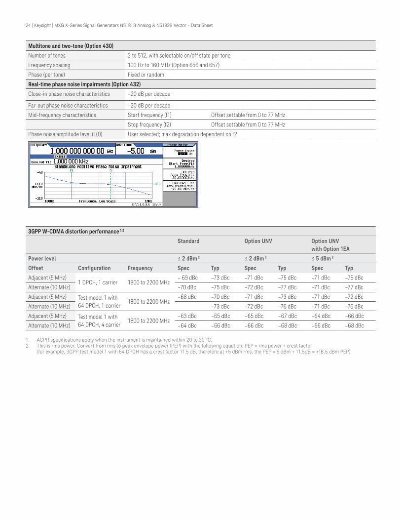
3GPP W-CDMA distortion performance 1,2
Standard Option UNV Option UNV with Option 1EA
Power level ≤ 2 dBm 2 ≤ 2 dBm 2 ≤ 5 dBm 2
Offset Configuration Frequency Spec Typ Spec Typ Spec Typ
Adjacent (5 MHz)1 DPCH, 1 carrier 1800 to 2200 MHz
– 69 dBc –73 dBc –71 dBc –75 dBc –71 dBc –75 dBc
Alternate (10 MHz) –70 dBc –75 dBc –72 dBc –77 dBc –71 dBc –77 dBc
Adjacent (5 MHz) Test model 1 with 64 DPCH, 1 carrier
1800 to 2200 MHz–68 dBc –70 dBc –71 dBc –73 dBc –71 dBc –72 dBc
Alternate (10 MHz) –73 dBc –72 dBc –76 dBc –71 dBc –76 dBc
Adjacent (5 MHz) Test model 1 with 64 DPCH, 4 carrier
1800 to 2200 MHz–63 dBc –65 dBc –65 dBc –67 dBc –64 dBc –66 dBc
Alternate (10 MHz) –64 dBc –66 dBc –66 dBc –68 dBc –66 dBc –68 dBc
1. ACPR specifications apply when the instrument is maintained within 20 to 30 °C.2. This is rms power. Convert from rms to peak envelope power (PEP) with the following equation: PEP = rms power + crest factor
(for example, 3GPP test model 1 with 64 DPCH has a crest factor 11.5 dB, therefore at +5 dBm rms, the PEP = 5 dBm + 11.5dB = +16.5 dBm PEP).
24 | Keysight | MXG X-Series Signal Generators N5181B Analog & N5182B Vector - Data Sheet
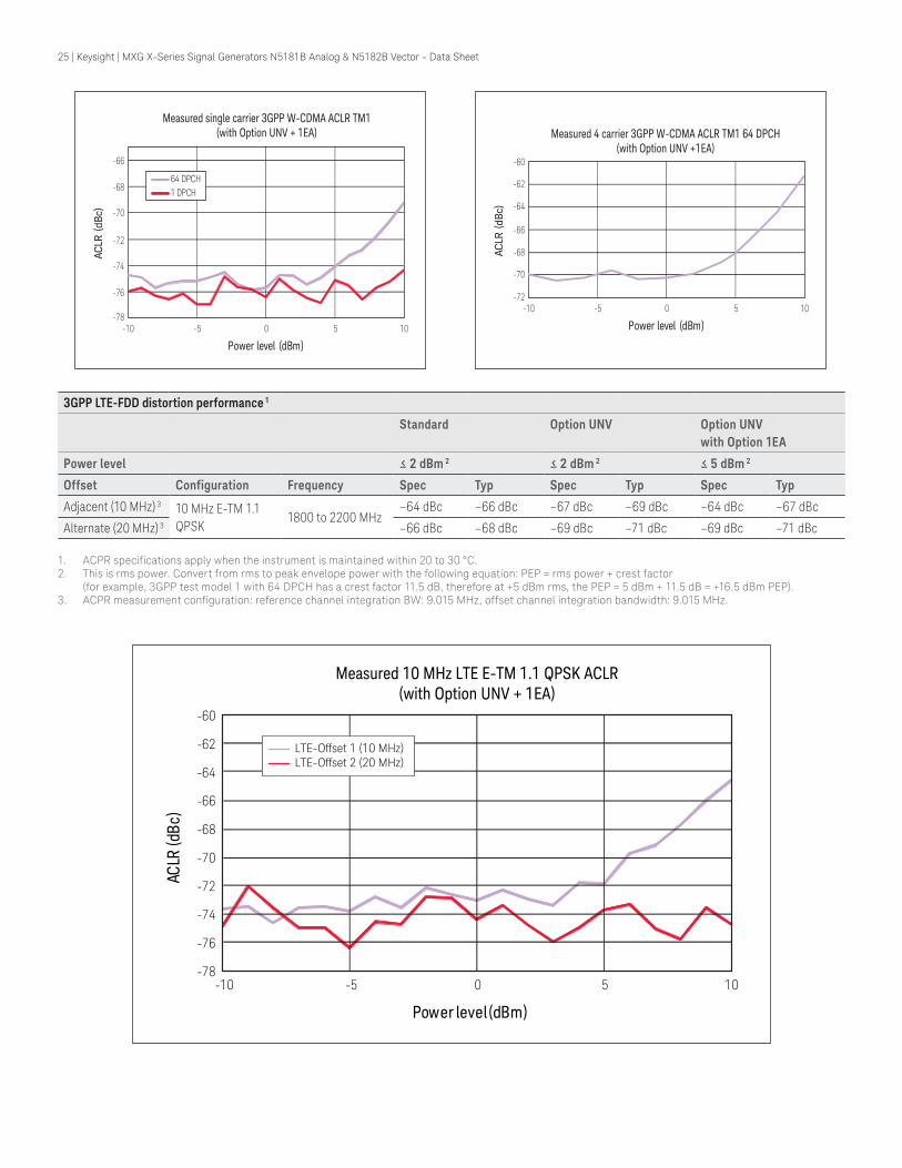
3GPP LTE-FDD distortion performance 1
Standard Option UNV Option UNV with Option 1EA
Power level ≤ 2 dBm 2 ≤ 2 dBm 2 ≤ 5 dBm 2
Offset Configuration Frequency Spec Typ Spec Typ Spec Typ
Adjacent (10 MHz) 3 10 MHz E-TM 1.1 QPSK
1800 to 2200 MHz–64 dBc –66 dBc –67 dBc –69 dBc –64 dBc –67 dBc
Alternate (20 MHz) 3 –66 dBc –68 dBc –69 dBc –71 dBc –69 dBc –71 dBc
1. ACPR specifications apply when the instrument is maintained within 20 to 30 °C.2. This is rms power. Convert from rms to peak envelope power with the following equation: PEP = rms power + crest factor
(for example, 3GPP test model 1 with 64 DPCH has a crest factor 11.5 dB, therefore at +5 dBm rms, the PEP = 5 dBm + 11.5 dB = +16.5 dBm PEP).3. ACPR measurement configuration: reference channel integration BW: 9.015 MHz, offset channel integration bandwidth: 9.015 MHz.
-78
-76
-74
-72
-70
-68
-66
-64
-62
-60
-10 -5 0 5 10
ACLR
(dBc
)
Power level (dBm)
Measured 10 MHz LTE E-TM 1.1 QPSK ACLR(with Option UNV + 1EA)
LTE-Offset 1 (10 MHz)LTE-Offset 2 (20 MHz)
-78
-76
-74
-72
-70
-66
-68
-10 -5 0 5 10
ACLR
(dB
c)
Power level (dBm)
Measured single carrier 3GPP W-CDMA ACLR TM1(with Option UNV + 1EA)
64 DPCH1 DPCH
-72
-70
-68
-66
-64
-62
-60
-10 -5 0 5 10
ACLR
(dB
c)
Power level (dBm)
Measured 4 carrier 3GPP W-CDMA ACLR TM1 64 DPCH(with Option UNV +1EA)
25 | Keysight | MXG X-Series Signal Generators N5181B Analog & N5182B Vector - Data Sheet
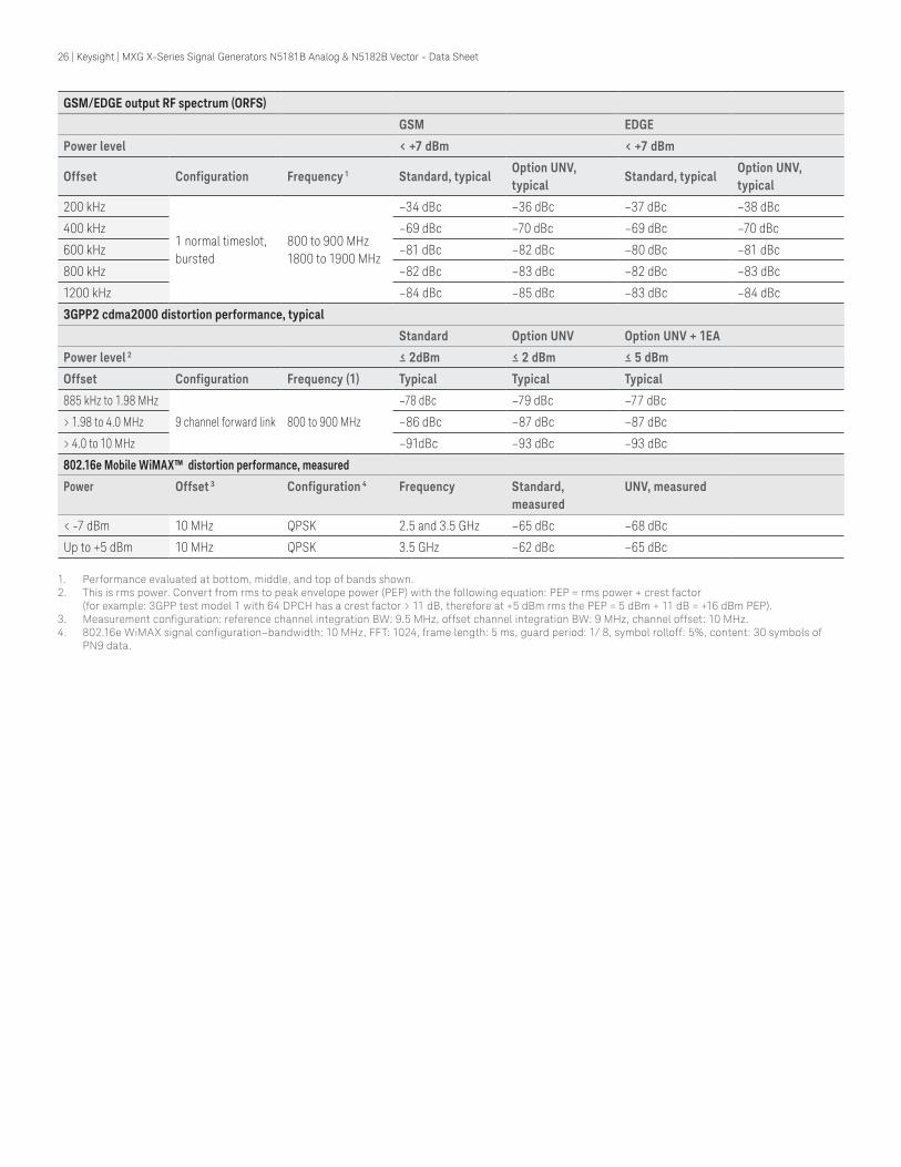
GSM/EDGE output RF spectrum (ORFS)
GSM EDGE
Power level < +7 dBm < +7 dBm
Offset Configuration Frequency 1 Standard, typicalOption UNV, typical
Standard, typicalOption UNV, typical
200 kHz
1 normal timeslot, bursted
800 to 900 MHz1800 to 1900 MHz
–34 dBc –36 dBc –37 dBc –38 dBc
400 kHz –69 dBc –70 dBc –69 dBc –70 dBc
600 kHz –81 dBc –82 dBc –80 dBc –81 dBc
800 kHz –82 dBc –83 dBc –82 dBc –83 dBc
1200 kHz –84 dBc –85 dBc –83 dBc –84 dBc
3GPP2 cdma2000 distortion performance, typical
Standard Option UNV Option UNV + 1EA
Power level 2 ≤ 2dBm ≤ 2 dBm ≤ 5 dBm
Offset Configuration Frequency (1) Typical Typical Typical
885 kHz to 1.98 MHz
9 channel forward link 800 to 900 MHz
–78 dBc –79 dBc –77 dBc
> 1.98 to 4.0 MHz –86 dBc –87 dBc –87 dBc
> 4.0 to 10 MHz –91dBc –93 dBc –93 dBc
802.16e Mobile WiMAX™ distortion performance, measured
Power Offset 3 Configuration 4 Frequency Standard, measured
UNV, measured
< -7 dBm 10 MHz QPSK 2.5 and 3.5 GHz –65 dBc –68 dBc
Up to +5 dBm 10 MHz QPSK 3.5 GHz –62 dBc –65 dBc
1. Performance evaluated at bottom, middle, and top of bands shown.2. This is rms power. Convert from rms to peak envelope power (PEP) with the following equation: PEP = rms power + crest factor
(for example: 3GPP test model 1 with 64 DPCH has a crest factor > 11 dB, therefore at +5 dBm rms the PEP = 5 dBm + 11 dB = +16 dBm PEP).3. Measurement configuration: reference channel integration BW: 9.5 MHz, offset channel integration BW: 9 MHz, channel offset: 10 MHz.4. 802.16e WiMAX signal configuration–bandwidth: 10 MHz, FFT: 1024, frame length: 5 ms, guard period: 1/ 8, symbol rolloff: 5%, content: 30 symbols of
PN9 data.
26 | Keysight | MXG X-Series Signal Generators N5181B Analog & N5182B Vector - Data Sheet
0.2
0.4
0.6
0.8
1
1.2
1.4
1.6
1.8
2
-15 -10 -5 0 5 10 15
EV
M (%
rm
s)
Power level (dBm)
Measured EVM performance vs. power801.11ac 160 MHz 256 QAM @ 5.25 GHz
Rx equalizer training preamble only(MXG factory channel corrections enabled)
0.2
0.4
0.6
0.8
1
1.2
1.4
1.6
1.8
2
-15 -10 -5 0 5 10 15
EV
M (%
rm
s)
Power level (dBm)
Measured EVM performance vs. power801.11ac 80 MHz 256 QAM @ 5.775 GHz
Rx equalizer training preamble only(MXG factory channel corrections enabled)
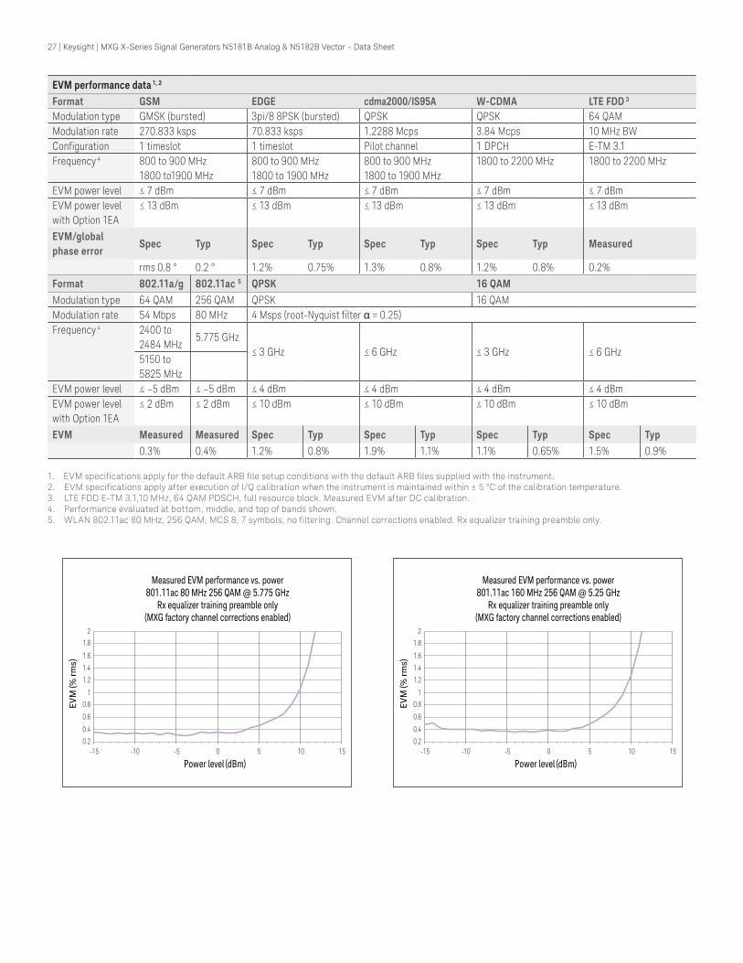
EVM performance data 1, 2
Format GSM EDGE cdma2000/IS95A W-CDMA LTE FDD 3
Modulation type GMSK (bursted) 3pi/8 8PSK (bursted) QPSK QPSK 64 QAMModulation rate 270.833 ksps 70.833 ksps 1.2288 Mcps 3.84 Mcps 10 MHz BWConfiguration 1 timeslot 1 timeslot Pilot channel 1 DPCH E-TM 3.1Frequency 4 800 to 900 MHz
1800 to1900 MHz800 to 900 MHz 1800 to 1900 MHz
800 to 900 MHz 1800 to 1900 MHz
1800 to 2200 MHz 1800 to 2200 MHz
EVM power level ≤ 7 dBm ≤ 7 dBm ≤ 7 dBm ≤ 7 dBm ≤ 7 dBmEVM power level with Option 1EA
≤ 13 dBm ≤ 13 dBm ≤ 13 dBm ≤ 13 dBm ≤ 13 dBm
EVM/global phase error
Spec Typ Spec Typ Spec Typ Spec Typ Measured
rms 0.8 ° 0.2 ° 1.2% 0.75% 1.3% 0.8% 1.2% 0.8% 0.2%
Format 802.11a/g 802.11ac 5 QPSK 16 QAMModulation type 64 QAM 256 QAM QPSK 16 QAMModulation rate 54 Mbps 80 MHz 4 Msps (root-Nyquist filter α = 0.25)Frequency 4 2400 to
2484 MHz5.775 GHz
≤ 3 GHz ≤ 6 GHz ≤ 3 GHz ≤ 6 GHz5150 to 5825 MHz
EVM power level ≤ –5 dBm ≤ –5 dBm ≤ 4 dBm ≤ 4 dBm ≤ 4 dBm ≤ 4 dBmEVM power level with Option 1EA
≤ 2 dBm ≤ 2 dBm ≤ 10 dBm ≤ 10 dBm ≤ 10 dBm ≤ 10 dBm
EVM Measured Measured Spec Typ Spec Typ Spec Typ Spec Typ0.3% 0.4% 1.2% 0.8% 1.9% 1.1% 1.1% 0.65% 1.5% 0.9%
1. EVM specifications apply for the default ARB file setup conditions with the default ARB files supplied with the instrument.2. EVM specifications apply after execution of I/Q calibration when the instrument is maintained within ± 5 °C of the calibration temperature.3. LTE FDD E-TM 3.1,10 MHz, 64 QAM PDSCH, full resource block. Measured EVM after DC calibration.4. Performance evaluated at bottom, middle, and top of bands shown.5. WLAN 802.11ac 80 MHz, 256 QAM, MCS 8, 7 symbols, no filtering. Channel corrections enabled. Rx equalizer training preamble only.
27 | Keysight | MXG X-Series Signal Generators N5181B Analog & N5182B Vector - Data Sheet
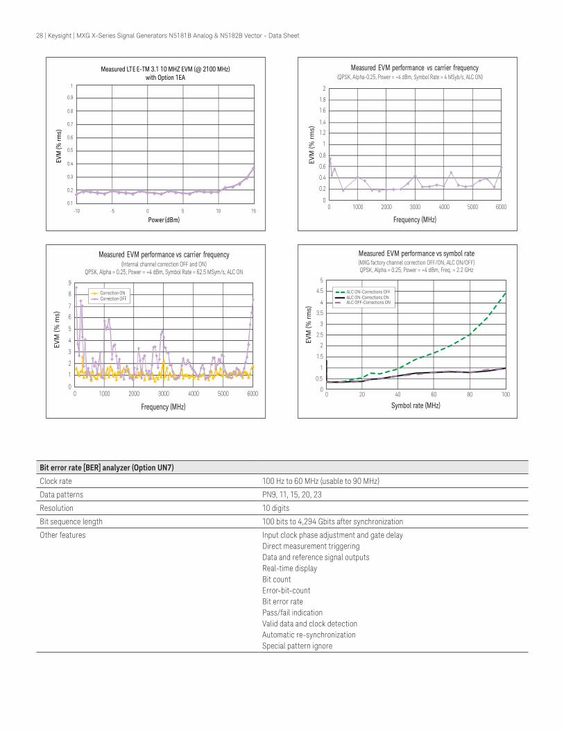
0.1
0.2
0.3
0.4
0.5
0.6
0.7
0.8
0.9
1
-10 -5 0 5 10 15
EVM
(% rm
s)
Power (dBm)
Measured LTE E-TM 3.1 10 MHZ EVM (@ 2100 MHz)with Option 1EA
0
0.2
0.4
0.6
0.8
1
1.2
1.4
1.6
1.8
2
0 2000 3000 4000 5000 60001000
EVM
(% r
ms)
Frequency (MHz)
Measured EVM performance vs carrier frequency(QPSK, Alpha-0.25, Power = +4 dBm, Symbol Rate = 4 MSyb/s, ALC ON)
0
1
2
3
4
5
6
7
8
9
0 2000 3000 4000 5000 60001000
EVM
(% m
s)
Frequency (MHz)
Measured EVM performance vs carrier frequency
Correction ONCorrection OFF
(Internal channel correction OFF and ON)QPSK, Alpha = 0.25, Power = +4 dBm, Symbol Rate = 62.5 MSym/s, ALC ON
0
0.5
1
1.5
2
3
2.5
3.5
4
4.5
5
0 40 60 80 10020
EVM
(% rm
s)
Symbol rate (MHz)
Measured EVM performance vs symbol rate(MXG factory channel correction OFF/ON, ALC ON/OFF)QPSK, Alpha = 0.25, Power = +4 dBm, Freq. = 2.2 GHz
ALC ON-Corrections OFFALC ON-Corrections ONALC OFF-Corrections ON
Bit error rate [BER] analyzer (Option UN7)
Clock rate 100 Hz to 60 MHz (usable to 90 MHz)
Data patterns PN9, 11, 15, 20, 23
Resolution 10 digits
Bit sequence length 100 bits to 4,294 Gbits after synchronization
Other features Input clock phase adjustment and gate delayDirect measurement triggeringData and reference signal outputsReal-time displayBit countError-bit-countBit error ratePass/fail indicationValid data and clock detectionAutomatic re-synchronizationSpecial pattern ignore
28 | Keysight | MXG X-Series Signal Generators N5181B Analog & N5182B Vector - Data Sheet
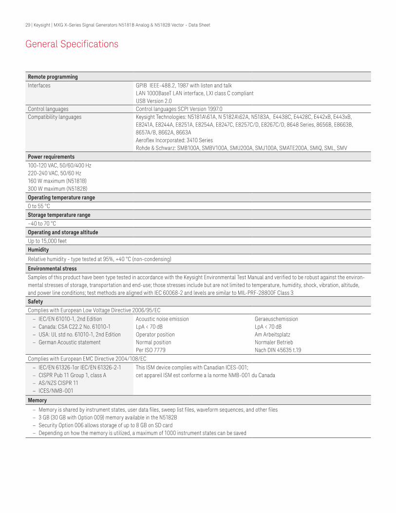
General Specifications
Remote programmingInterfaces GPIB IEEE-488.2, 1987 with listen and talk
LAN 1000BaseT LAN interface, LXI class C compliantUSB Version 2.0
Control languages Control languages SCPI Version 1997.0Compatibility languages Keysight Technologies: N5181A\61A, N 5182A\62A, N5183A, E4438C, E4428C, E442xB, E443xB,
E8241A, E8244A, E8251A, E8254A, E8247C, E8257C/D, E8267C/D, 8648 Series, 8656B, E8663B, 8657A/B, 8662A, 8663AAeroflex Incorporated: 3410 SeriesRohde & Schwarz: SMB100A, SMBV100A, SMU200A, SMJ100A, SMATE200A, SMIQ, SML, SMV
Power requirements100-120 VAC, 50/60/400 Hz 220-240 VAC, 50/60 Hz 160 W maximum (N5181B) 300 W maximum (N5182B)
Operating temperature range0 to 55 °C
Storage temperature range–40 to 70 °C
Operating and storage altitudeUp to 15,000 feet
Humidity
Relative humidity - type tested at 95%, +40 °C (non-condensing)
Environmental stressSamples of this product have been type tested in accordance with the Keysight Environmental Test Manual and verified to be robust against the environ-mental stresses of storage, transportation and end-use; those stresses include but are not limited to temperature, humidity, shock, vibration, altitude, and power line conditions; test methods are aligned with IEC 60068-2 and levels are similar to MIL-PRF-28800F Class 3
SafetyComplies with European Low Voltage Directive 2006/95/EC
– IEC/EN 61010-1, 2nd Edition – Canada: CSA C22.2 No. 61010-1 – USA: UL std no. 61010-1, 2nd Edition – German Acoustic statement
Acoustic noise emissionLpA < 70 dBOperator positionNormal positionPer ISO 7779
GeraeuschemissionLpA < 70 dBAm ArbeitsplatzNormaler BetriebNach DIN 45635 t.19
Complies with European EMC Directive 2004/108/EC
– IEC/EN 61326-1or IEC/EN 61326-2-1 – CISPR Pub 11 Group 1, class A – AS/NZS CISPR 11 – ICES/NMB-001
This ISM device complies with Canadian ICES-001; cet appareil ISM est conforme a la norme NMB-001 du Canada
Memory
– Memory is shared by instrument states, user data files, sweep list files, waveform sequences, and other files – 3 GB (30 GB with Option 009) memory available in the N5182B – Security Option 006 allows storage of up to 8 GB on SD card – Depending on how the memory is utilized, a maximum of 1000 instrument states can be saved
29 | Keysight | MXG X-Series Signal Generators N5181B Analog & N5182B Vector - Data Sheet
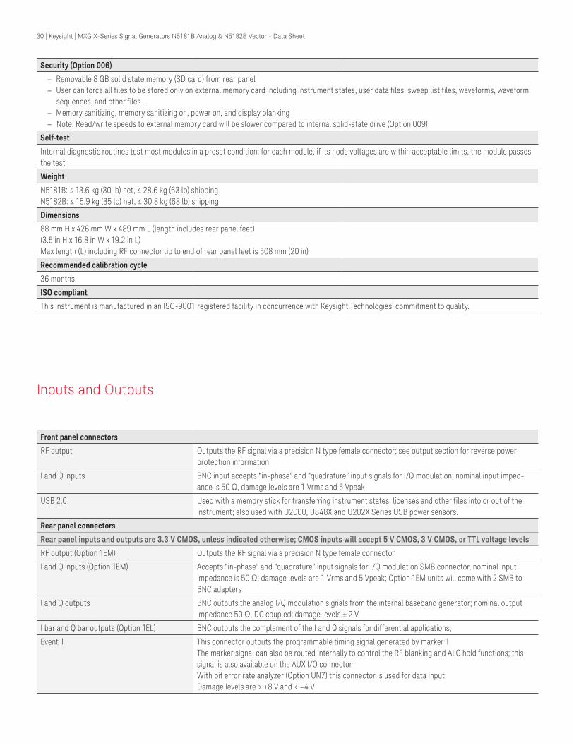
Security (Option 006)
– Removable 8 GB solid state memory (SD card) from rear panel – User can force all files to be stored only on external memory card including instrument states, user data files, sweep list files, waveforms, waveform
sequences, and other files. – Memory sanitizing, memory sanitizing on, power on, and display blanking – Note: Read/write speeds to external memory card will be slower compared to internal solid-state drive (Option 009)
Self-test
Internal diagnostic routines test most modules in a preset condition; for each module, if its node voltages are within acceptable limits, the module passes the test
Weight
N5181B: ≤ 13.6 kg (30 lb) net, ≤ 28.6 kg (63 lb) shippingN5182B: ≤ 15.9 kg (35 lb) net, ≤ 30.8 kg (68 lb) shipping
Dimensions
88 mm H x 426 mm W x 489 mm L (length includes rear panel feet) (3.5 in H x 16.8 in W x 19.2 in L)Max length (L) including RF connector tip to end of rear panel feet is 508 mm (20 in)
Recommended calibration cycle
36 months
ISO compliant
This instrument is manufactured in an ISO-9001 registered facility in concurrence with Keysight Technologies’ commitment to quality.
Inputs and Outputs
Front panel connectors
RF output Outputs the RF signal via a precision N type female connector; see output section for reverse power protection information
I and Q inputs BNC input accepts “in-phase” and “quadrature” input signals for I/Q modulation; nominal input imped-ance is 50 Ω, damage levels are 1 Vrms and 5 Vpeak
USB 2.0 Used with a memory stick for transferring instrument states, licenses and other files into or out of the instrument; also used with U2000, U848X and U202X Series USB power sensors.
Rear panel connectors
Rear panel inputs and outputs are 3.3 V CMOS, unless indicated otherwise; CMOS inputs will accept 5 V CMOS, 3 V CMOS, or TTL voltage levels
RF output (Option 1EM) Outputs the RF signal via a precision N type female connector
I and Q inputs (Option 1EM) Accepts “in-phase” and “quadrature” input signals for I/Q modulation SMB connector, nominal input impedance is 50 Ω; damage levels are 1 Vrms and 5 Vpeak; Option 1EM units will come with 2 SMB to BNC adapters
I and Q outputs BNC outputs the analog I/Q modulation signals from the internal baseband generator; nominal output impedance 50 Ω, DC coupled; damage levels ± 2 V
I bar and Q bar outputs (Option 1EL) BNC outputs the complement of the I and Q signals for differential applications;
Event 1 This connector outputs the programmable timing signal generated by marker 1The marker signal can also be routed internally to control the RF blanking and ALC hold functions; this signal is also available on the AUX I/O connectorWith bit error rate analyzer (Option UN7) this connector is used for data inputDamage levels are > +8 V and < –4 V
30 | Keysight | MXG X-Series Signal Generators N5181B Analog & N5182B Vector - Data Sheet
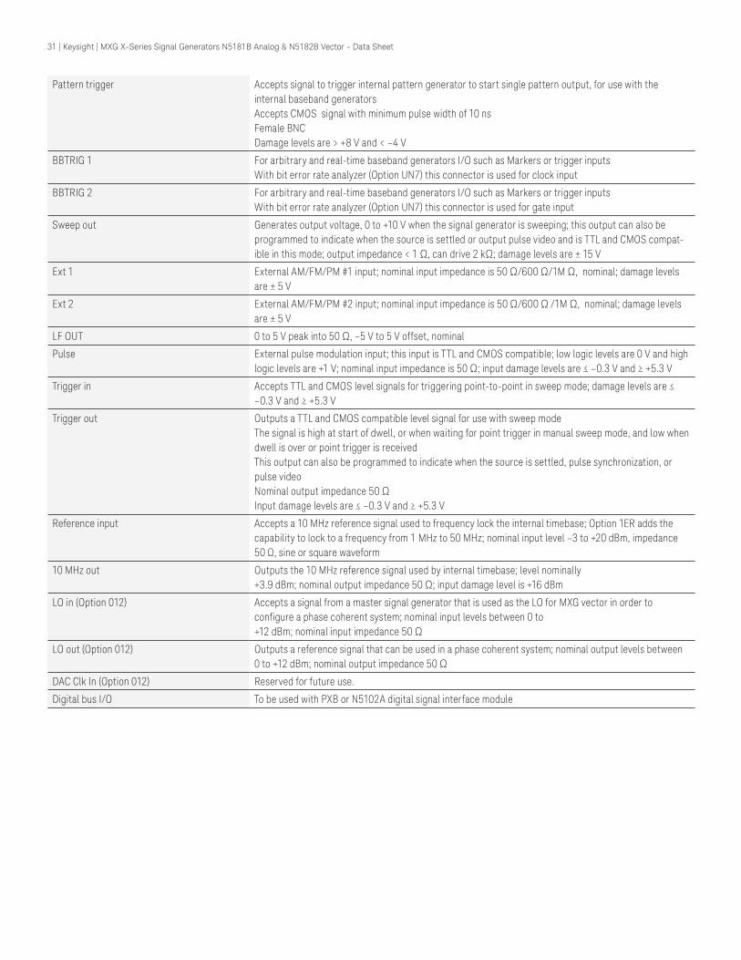
Pattern trigger Accepts signal to trigger internal pattern generator to start single pattern output, for use with the internal baseband generatorsAccepts CMOS signal with minimum pulse width of 10 nsFemale BNCDamage levels are > +8 V and < –4 V
BBTRIG 1 For arbitrary and real-time baseband generators I/O such as Markers or trigger inputsWith bit error rate analyzer (Option UN7) this connector is used for clock input
BBTRIG 2 For arbitrary and real-time baseband generators I/O such as Markers or trigger inputsWith bit error rate analyzer (Option UN7) this connector is used for gate input
Sweep out Generates output voltage, 0 to +10 V when the signal generator is sweeping; this output can also be programmed to indicate when the source is settled or output pulse video and is TTL and CMOS compat-ible in this mode; output impedance < 1 Ω, can drive 2 kΩ; damage levels are ± 15 V
Ext 1 External AM/FM/PM #1 input; nominal input impedance is 50 Ω/600 Ω/1M Ω, nominal; damage levels are ± 5 V
Ext 2 External AM/FM/PM #2 input; nominal input impedance is 50 Ω/600 Ω /1M Ω, nominal; damage levels are ± 5 V
LF OUT 0 to 5 V peak into 50 Ω, –5 V to 5 V offset, nominal
Pulse External pulse modulation input; this input is TTL and CMOS compatible; low logic levels are 0 V and high logic levels are +1 V; nominal input impedance is 50 Ω; input damage levels are ≤ –0.3 V and ≥ +5.3 V
Trigger in Accepts TTL and CMOS level signals for triggering point-to-point in sweep mode; damage levels are ≤ –0.3 V and ≥ +5.3 V
Trigger out Outputs a TTL and CMOS compatible level signal for use with sweep modeThe signal is high at start of dwell, or when waiting for point trigger in manual sweep mode, and low when dwell is over or point trigger is receivedThis output can also be programmed to indicate when the source is settled, pulse synchronization, or pulse videoNominal output impedance 50 ΩInput damage levels are ≤ –0.3 V and ≥ +5.3 V
Reference input Accepts a 10 MHz reference signal used to frequency lock the internal timebase; Option 1ER adds the capability to lock to a frequency from 1 MHz to 50 MHz; nominal input level –3 to +20 dBm, impedance 50 Ω, sine or square waveform
10 MHz out Outputs the 10 MHz reference signal used by internal timebase; level nominally +3.9 dBm; nominal output impedance 50 Ω; input damage level is +16 dBm
LO in (Option 012) Accepts a signal from a master signal generator that is used as the LO for MXG vector in order to configure a phase coherent system; nominal input levels between 0 to+12 dBm; nominal input impedance 50 Ω
LO out (Option 012) Outputs a reference signal that can be used in a phase coherent system; nominal output levels between 0 to +12 dBm; nominal output impedance 50 Ω
DAC Clk In (Option 012) Reserved for future use.
Digital bus I/O To be used with PXB or N5102A digital signal interface module
31 | Keysight | MXG X-Series Signal Generators N5181B Analog & N5182B Vector - Data Sheet
Aux I/O Aux I/O port sends and/or receives auxiliary signaling information:For Option UN7 this connector is used to output reference data, clock, error signals, and moreOutput markers to an external device from arbitrary waveform or real-time generation application such as: frame markers, pulse-per-second, even-second, and more. Input signals from external DUT to modify characteristics of a signal being generated such as changing output power (power control loop testing), advancing or delaying timing (timing advance loop testing), HARQ ACK/NAK delivery (HARQ process loop testing) or streaming external data, clock and symbol synch for custom modulation.I/O is application specific (CDMA, 3GPP, GNSS, LTE, custom). See User Guide or Signal Studio help for more details.Connector type: 36 pin 3M connector (part number N10236-52B2PC). The mating connector is a 3M 10136-3000 wire mount plug or 3M 10136-8000 IDC plug with a 3M 10336 shell.
For Option 431 real-time custom modulation the follow pin numbers are assigned:Data input = pin 23Data clock input = pin 29Symbol sync input = pin 25Burst input = pin 27Data output = pin 35Data clock output = pin 6Symbol sync output = pin 37Event 1 output = pin 1Event 2 output = pin 33
USB 2.0 The USB connector provides remote programming functions via SCPI
LAN (1000 BaseT) The LAN connector provides the same SCPI remote programming functionality as the GPIB connector and is also used to access the internal Web server and FTP serverSupports DHCP, sockets SCPI, VXI-11 SCPI, connection monitoring, dynamic hostname services, TCP keep aliveLXI class C compliantTrigger response time for the immediate LAN trigger is 0.5 ms (minimum), 4 ms (maximum), 2 ms, typical; delayed/alarm triger is unknownTrigger output response time is 0.5 ms (minimum), 4 ms (maximum), 2 ms, typical
GPIB The GPIB connector provides remote programming functionality via SCPI
Related Literature
Keysight X-Series Signal Generators
MXG Configuration Guide 5990-9959EN
EXG Data Sheet 5991-0039EN
EXG Configuration Guide 5990-9958EN
X-Series Signal Generator Brochure 5990-9957EN
Signal Studio Software Brochure 5989-6448EN
32 | Keysight | MXG X-Series Signal Generators N5181B Analog & N5182B Vector - Data Sheet
33 | Keysight | MXG X-Series Signal Generators N5181B Analog & N5182B Vector - Data Sheet
This information is subject to change without notice.© Keysight Technologies, 2012 - 2016Published in USA, July 22, 20165991-0038ENwww.keysight.com
myKeysight
www.keysight.com/find/mykeysightA personalized view into the information most relevant to you.
Keysight Infoline
www.keysight.com/find/InfolineKeysight’s insight to best in class information management. Free access to your Keysight equipment company reports and e-library.
KEYSIGHT SERVICES
Keysight Serviceswww.keysight.com/find/servicesOur deep offering in design, test, and measurement services deploys an industry-leading array of people, processes, and tools. The result? We help you implement new technologies and engineer improved processes that lower costs.
Three-Year Warranty
www.keysight.com/find/ThreeYearWarrantyKeysight’s committed to superior product quality and lower total cost of ownership. Keysight is the only test and measurement company with three-year warranty standard on all instruments, worldwide. And, we provide a one-year warranty on many accessories, calibration devices, systems and custom products.
Keysight Assurance Plans
www.keysight.com/find/AssurancePlansUp to ten years of protection and no budgetary surprises to ensure your instruments are operating to specification, so you can rely on accurate measurements.
Keysight Channel Partnerswww.keysight.com/find/channelpartnersGet the best of both worlds: Keysight’s measurement expertise and product breadth, combined with channel partner convenience.
cdma2000 is a US registered certification mark of the Telecommunications Industry Association.
WiMAX is a US trademark of the WiMAX Forum.
Bluetooth and the Bluetooth logos are trademarks owned by Bluetooth SIG, Inc., U.S.A. and licensed to Keysight Technologies, Inc.
www.keysight.com/find/mxg
For more information on Keysight Technologies’ products, applications or services, please contact your local Keysight office. The complete list is available at:www.keysight.com/find/contactus
Americas Canada (877) 894 4414Brazil 55 11 3351 7010Mexico 001 800 254 2440United States (800) 829 4444
Asia PacificAustralia 1 800 629 485China 800 810 0189Hong Kong 800 938 693India 1 800 11 2626Japan 0120 (421) 345Korea 080 769 0800Malaysia 1 800 888 848Singapore 1 800 375 8100Taiwan 0800 047 866Other AP Countries (65) 6375 8100
Europe & Middle EastAustria 0800 001122Belgium 0800 58580Finland 0800 523252France 0805 980333Germany 0800 6270999Ireland 1800 832700Israel 1 809 343051Italy 800 599100Luxembourg +32 800 58580Netherlands 0800 0233200Russia 8800 5009286Spain 800 000154Sweden 0200 882255Switzerland 0800 805353
Opt. 1 (DE)Opt. 2 (FR)Opt. 3 (IT)
United Kingdom 0800 0260637
For other unlisted countries:www.keysight.com/find/contactus(BP-06-08-16)
DEKRA CertifiedISO9001 Quality Management System
www.keysight.com/go/qualityKeysight Technologies, Inc.DEKRA Certified ISO 9001:2015Quality Management System
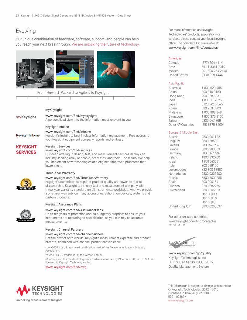
Evolving Our unique combination of hardware, software, support, and people can help you reach your next breakthrough. We are unlocking the future of technology.
From Hewlett-Packard to Agilent to Keysight