Embed Size (px)
Citation preview
SN74HC4851-Q1 8-CHANNEL ANALOG MULTIPLEXER/DEMULTIPLEXER
WITH INJECTION-CURRENT EFFECT CONTROL SCLS554C − JANUARY 2004 − REVISED OCTOBER 2012
testing of all parameters.
POST OFFICE BOX 655303 • DALLAS, TEXAS 75265 1
• Qualified for Automotive Applications • Injection-Current Cross Coupling <1mV/mA
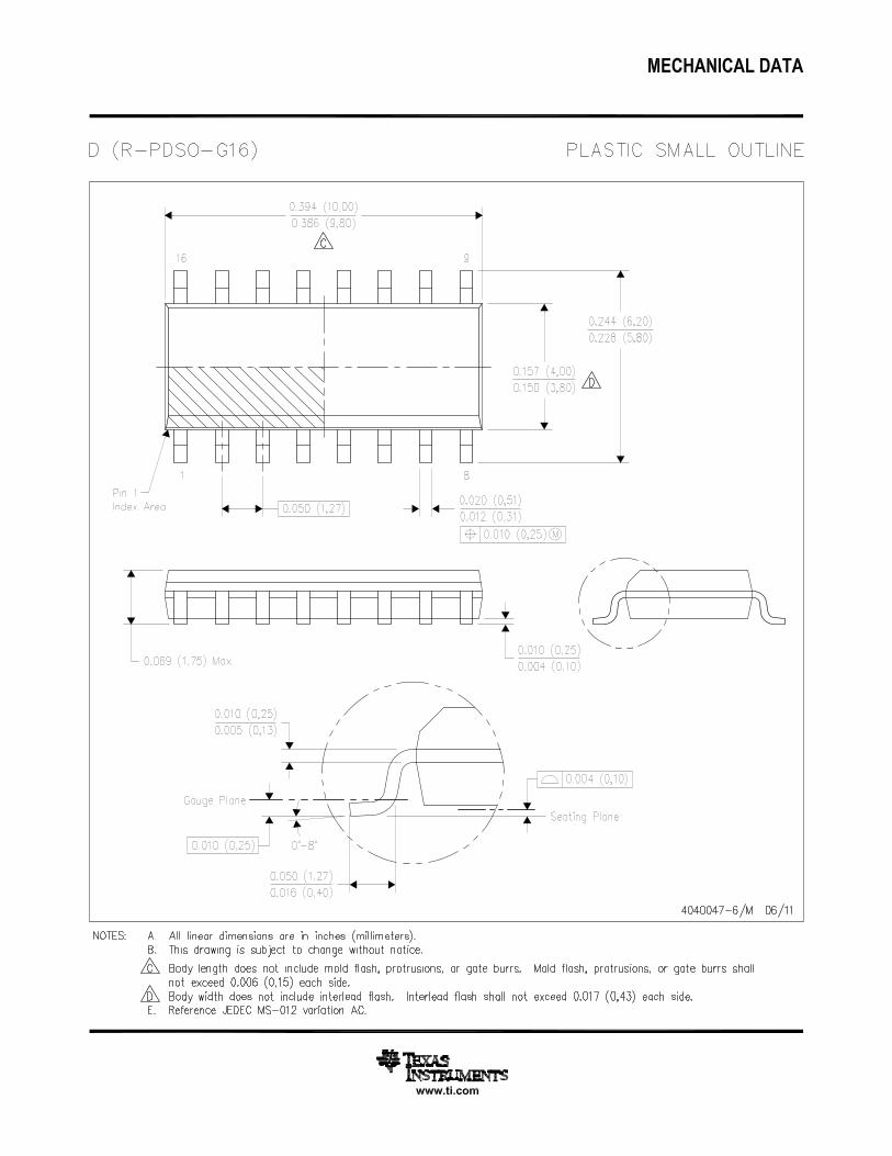
D OR PW PACKAGE
(TOP VIEW)
(see Figure 1) • Low Crosstalk Between Switches • Pin Compatible With CD74HC4051,
SN74LV4051A, and CD4051B • 2-V to 6-V VCC Operation • Latch-Up Performance Exceeds 100 mA Per
JESD 78, Class II
Y4 1 Y6 2
COM 3 Y7 4 Y5 5
INH 6 NC 7
GND 8
16 VCC
15 Y2 14 Y1 13 Y0 12 Y3 11 A 10 B 9 C
description/ordering information NC − No internal connection
This eight-channel CMOS analog multiplexer/demultiplexer is pin compatible with the ’4051 function and, additionally, features injection-current effect control, which has excellent value in automotive applications where voltages in excess of normal supply voltages are common.
The injection-current effect control allows signals at disabled analog input channels to exceed the supply voltage without affecting the signal of the enabled analog channel. This eliminates the need for external diode/resistor networks typically used to keep the analog channel signals within the supply-voltage range.
ORDERING INFORMATIONt
TA
PACKAGE‡ ORDERABLE PART NUMBER
TOP-SIDE MARKING
−40°C to 125°C
SOIC − D Tape and reel SN74HC4851QDRQ1 HC4851Q TSSOP − PW Tape and reel SN74HC4851QPWRQ1 HC4851Q TSSOP − PW Tape and reel SN74HC4851QPWRG4Q1 HC4851Q
† For the most current package and ordering information, see the Package Option Addendum at the end of this document, or see the TI web site at http://www.ti.com.
‡ Package drawings, thermal data, and symbolization are available at http://www.ti.com/packaging.
FUNCTION TABLE
INPUTS ON CHANNEL INH C B A
L L L L
L L L H
L L H L
L L H H
L H L L
L H L H
L H H L
L H H H
H X X X
Y0
Y1
Y2
Y3
Y4
Y5
Y6
Y7
None
Please be aware that an important notice concerning availability, standard warranty, and use in critical applications of Texas Instruments semiconductor products and disclaimers thereto appears at the end of this data sheet.
PRODUCTION DATA information is current as of publication date. Products conform to specifications per the terms of Texas Instruments standard warranty. Production processing does not necessarily include
Copyright © 2008−2012, Texas Instruments Incorporated
SN74HC4851-Q1 8-CHANNEL ANALOG MULTIPLEXER/DEMULTIPLEXER WITH INJECTION-CURRENT EFFECT CONTROL SCLS554C − JANUARY 2004 − REVISED SEPTEMBER 2012
POST OFFICE BOX 655303 • DALLAS, TEXAS 75265 2
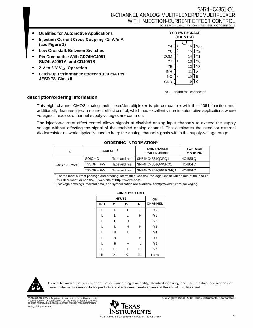
logic diagram (positive logic)
Injection− Current Control
Injection− Current Control
3
COM 13
Y0
11 A
10 B
C 9
INH 6
Injection− Current Control
Injection− Current Control
Injection− Current Control
Injection− Current Control
Injection− Current Control
Injection− Current Control
Injection− Current Control
14 Y1
15 Y2 12 Y3
1 Y4
5 Y5
2 Y6
4 Y7
SN74HC4851-Q1 8-CHANNEL ANALOG MULTIPLEXER/DEMULTIPLEXER
WITH INJECTION-CURRENT EFFECT CONTROL SCLS554C − JANUARY 2004 − REVISED OCTOBER 2012
POST OFFICE BOX 655303 • DALLAS, TEXAS 75265 3
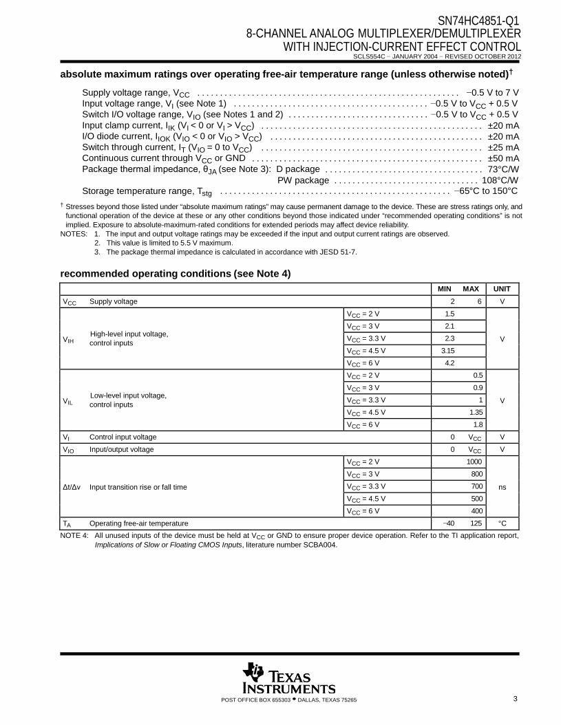
absolute maximum ratings over operating free-air temperature range (unless otherwise noted)†
Supply voltage range, VCC
. . . . . . . . . . . . . . . . . . . . . . . . . . . . . . . . . . . . . . . . . . . . . . . . . . . . . . . . . .
−0.5 V to 7 V
Input voltage range, VI (see Note 1) . . . . . . . . . . . . . . . . . . . . . . . . . . . . . . . . . . . . . . . . . . . −0.5 V to VCC + 0.5 V Switch I/O voltage range, VIO (see Notes 1 and 2) . . . . . . . . . . . . . . . . . . . . . . . . . . . . . . . −0.5 V to VCC + 0.5 V Input clamp current, IIK (VI < 0 or VI > VCC) . . . . . . . . . . . . . . . . . . . . . . . . . . . . . . . . . . . . . . . . . . . . . . . . . ±20 mA I/O diode current, IIOK (VIO < 0 or VIO > VCC) . . . . . . . . . . . . . . . . . . . . . . . . . . . . . . . . . . . . . . . . . . . . . . . ±20 mA Switch through current, IT (VIO = 0 to VCC) . . . . . . . . . . . . . . . . . . . . . . . . . . . . . . . . . . . . . . . . . . . . . . . . . ±25 mA Continuous current through VCC or GND . . . . . . . . . . . . . . . . . . . . . . . . . . . . . . . . . . . . . . . . . . . . . . . . . . . ±50 mA Package thermal impedance, θJA (see Note 3): D package . . . . . . . . . . . . . . . . . . . . . . . . . . . . . . . . . . . 73°C/W
PW package . . . . . . . . . . . . . . . . . . . . . . . . . . . . . . . . 108°C/W Storage temperature range, Tstg . . . . . . . . . . . . . . . . . . . . . . . . . . . . . . . . . . . . . . . . . . . . . . . . . . . −65°C to 150°C
† Stresses beyond those listed under “absolute maximum ratings” may cause permanent damage to the device. These are stress ratings only, and functional operation of the device at these or any other conditions beyond those indicated under “recommended operating conditions” is not implied. Exposure to absolute-maximum-rated conditions for extended periods may affect device reliability.
NOTES: 1. The input and output voltage ratings may be exceeded if the input and output current ratings are observed. 2. This value is limited to 5.5 V maximum. 3. The package thermal impedance is calculated in accordance with JESD 51-7.
recommended operating conditions (see Note 4)
MIN MAX UNIT VCC Supply voltage 2 6 V
High-level input voltage, VIH control inputs
VCC = 2 V 1.5
V VCC = 3 V 2.1 VCC = 3.3 V 2.3 VCC = 4.5 V 3.15 VCC = 6 V 4.2
Low-level input voltage, VIL control inputs
VCC = 2 V 0.5
V VCC = 3 V 0.9 VCC = 3.3 V 1 VCC = 4.5 V 1.35 VCC = 6 V 1.8
VI Control input voltage 0 VCC V VIO Input/output voltage 0 VCC V
Δt/Δv Input transition rise or fall time
VCC = 2 V 1000
ns VCC = 3 V 800 VCC = 3.3 V 700 VCC = 4.5 V 500 VCC = 6 V 400
TA Operating free-air temperature −40 125 °C NOTE 4: All unused inputs of the device must be held at VCC or GND to ensure proper device operation. Refer to the TI application report,
Implications of Slow or Floating CMOS Inputs, literature number SCBA004.
SN74HC4851-Q1 8-CHANNEL ANALOG MULTIPLEXER/DEMULTIPLEXER WITH INJECTION-CURRENT EFFECT CONTROL SCLS554C − JANUARY 2004 − REVISED SEPTEMBER 2012
POST OFFICE BOX 655303 • DALLAS, TEXAS 75265 4
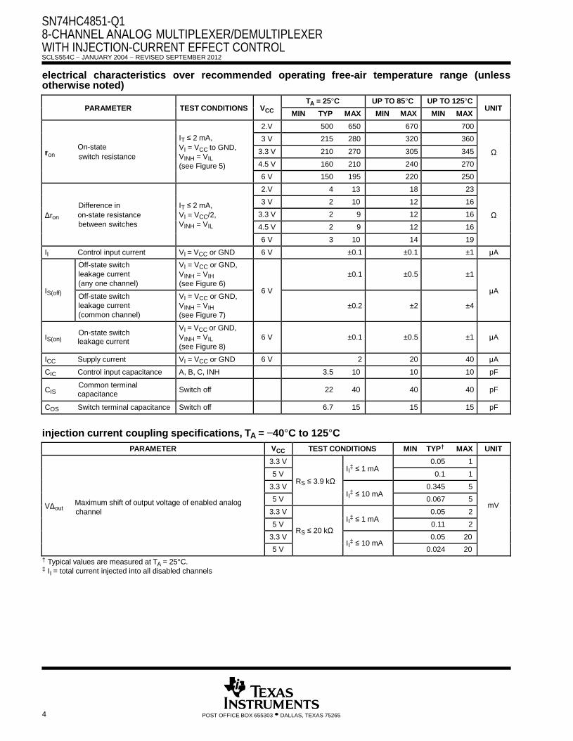
PARAMETER
TEST CONDITIONS
VCC
TA = 25°C UP TO 85°C UP TO 125°C UNIT
MIN TYP MAX MIN MAX MIN MAX r
On-state IT ≤ 2 mA, VI = VCC to GND, VINH = VIL (see Figure 5)
2.V 500 650 670 700
Ω 3 V 215 280 320 360
3.3 V 210 270 305 345 4.5 V 160 210 240 270 6 V 150 195 220 250
Difference in Δron on-state resistance
between switches
IT ≤ 2 mA, VI = VCC/2, VINH = VIL
2.V 4 13 18 23
Ω 3 V 2 10 12 16
3.3 V 2 9 12 16 4.5 V 2 9 12 16 6 V 3 10 14 19
II Control input current VI = VCC or GND 6 V ±0.1 ±0.1 ±1 μA IS(off)
Off-state switch leakage current (any one channel)
VI = VCC or GND, VINH = VIH (see Figure 6)
6 V
±0.1
±0.5
±1
μA Off-state switch leakage current (common channel)
VI = VCC or GND, VINH = VIH (see Figure 7)
±0.2
±2
±4
On-state switch
IS(on) leakage current VI = VCC or GND, VINH = VIL (see Figure 8)
6 V
±0.1
±0.5
±1
μA
ICC Supply current VI = VCC or GND 6 V 2 20 40 μA CIC Control input capacitance A, B, C, INH 3.5 10 10 10 pF
Common terminal CIS capacitance Switch off
22 40
40
40
pF COS Switch terminal capacitance Switch off 6.7 15 15 15 pF
electrical characteristics over recommended operating free-air temperature range (unless otherwise noted)
ron switch resistance
injection current coupling specifications, TA = −40°C to 125°C
PARAMETER VCC TEST CONDITIONS MIN TYP† MAX UNIT
VΔout
Maximum shift of output voltage of enabled analog channel
3.3 V RS ≤ 3.9 kΩ
II‡ ≤ 1 mA 0.05 1
mV
5 V 0.1 1 3.3 V
II‡ ≤ 10 mA 0.345 5
5 V 0.067 5 3.3 V
RS ≤ 20 kΩ
II‡ ≤ 1 mA
0.05 2 5 V 0.11 2
3.3 V II‡ ≤ 10 mA 0.05 20
5 V 0.024 20 † Typical values are measured at TA = 25°C. ‡ II = total current injected into all disabled channels
SN74HC4851-Q1 8-CHANNEL ANALOG MULTIPLEXER/DEMULTIPLEXER
WITH INJECTION-CURRENT EFFECT CONTROL SCLS554C − JANUARY 2004 − REVISED OCTOBER 2012
POST OFFICE BOX 655303 • DALLAS, TEXAS 75265 5
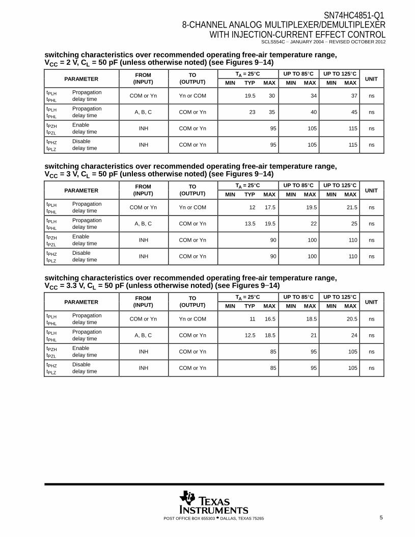
switching characteristics over recommended operating free-air temperature range, VCC = 2 V, CL = 50 pF (unless otherwise noted) (see Figures 9−14)
PARAMETER FROM
(INPUT) TO
(OUTPUT) TA = 25°C UP TO 85°C UP TO 125°C
UNIT MIN TYP MAX MIN MAX MIN MAX
tPLH Propagation tPHL delay time
COM or Yn
Yn or COM
19.5 30
34
37
ns
tPLH Propagation tPHL delay time
A, B, C
COM or Yn
23 35
40
45
ns
tPZH Enable tPZL delay time
INH
COM or Yn
95
105
115
ns
tPHZ Disable tPLZ delay time
INH
COM or Yn
95
105
115
ns
switching characteristics over recommended operating free-air temperature range, VCC = 3 V, CL = 50 pF (unless otherwise noted) (see Figures 9−14)
PARAMETER FROM
(INPUT) TO
(OUTPUT) TA = 25°C UP TO 85°C UP TO 125°C
UNIT MIN TYP MAX MIN MAX MIN MAX
tPLH Propagation tPHL delay time
COM or Yn
Yn or COM
12 17.5
19.5
21.5
ns
tPLH Propagation tPHL delay time
A, B, C
COM or Yn
13.5 19.5
22
25
ns
tPZH Enable tPZL delay time
INH
COM or Yn
90
100
110
ns
tPHZ Disable tPLZ delay time
INH
COM or Yn
90
100
110
ns
switching characteristics over recommended operating free-air temperature range, VCC = 3.3 V, CL = 50 pF (unless otherwise noted) (see Figures 9−14)
PARAMETER FROM
(INPUT) TO
(OUTPUT) TA = 25°C UP TO 85°C UP TO 125°C
UNIT MIN TYP MAX MIN MAX MIN MAX
tPLH Propagation tPHL delay time
COM or Yn
Yn or COM
11 16.5
18.5
20.5
ns
tPLH Propagation tPHL delay time
A, B, C
COM or Yn
12.5 18.5
21
24
ns
tPZH Enable tPZL delay time
INH
COM or Yn
85
95
105
ns
tPHZ Disable tPLZ delay time
INH
COM or Yn
85
95
105
ns
SN74HC4851-Q1 8-CHANNEL ANALOG MULTIPLEXER/DEMULTIPLEXER WITH INJECTION-CURRENT EFFECT CONTROL SCLS554C − JANUARY 2004 − REVISED SEPTEMBER 2012
POST OFFICE BOX 655303 • DALLAS, TEXAS 75265 6
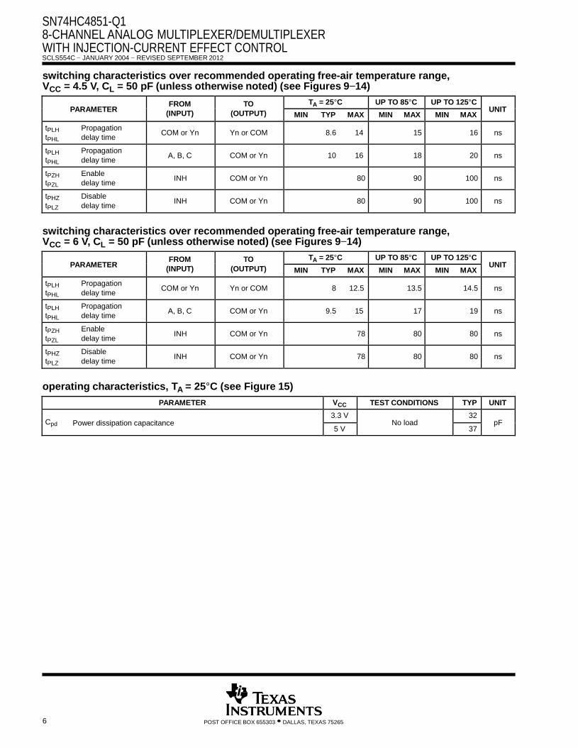
switching characteristics over recommended operating free-air temperature range, VCC = 4.5 V, CL = 50 pF (unless otherwise noted) (see Figures 9−14)
PARAMETER FROM
(INPUT) TO
(OUTPUT) TA = 25°C UP TO 85°C UP TO 125°C
UNIT MIN TYP MAX MIN MAX MIN MAX
tPLH Propagation tPHL delay time
COM or Yn
Yn or COM
8.6 14
15
16
ns
tPLH Propagation tPHL delay time
A, B, C
COM or Yn
10 16
18
20
ns
tPZH Enable tPZL delay time
INH
COM or Yn
80
90
100
ns
tPHZ Disable tPLZ delay time
INH
COM or Yn
80
90
100
ns
switching characteristics over recommended operating free-air temperature range, VCC = 6 V, CL = 50 pF (unless otherwise noted) (see Figures 9−14)
PARAMETER FROM
(INPUT) TO
(OUTPUT) TA = 25°C UP TO 85°C UP TO 125°C
UNIT MIN TYP MAX MIN MAX MIN MAX
tPLH Propagation tPHL delay time
COM or Yn
Yn or COM
8 12.5
13.5
14.5
ns
tPLH Propagation tPHL delay time
A, B, C
COM or Yn
9.5 15
17
19
ns
tPZH Enable tPZL delay time
INH
COM or Yn
78
80
80
ns
tPHZ Disable tPLZ delay time
INH
COM or Yn
78
80
80
ns
operating characteristics, TA = 25°C (see Figure 15)
PARAMETER VCC TEST CONDITIONS TYP UNIT Cpd Power dissipation capacitance
3.3 V No load 32
pF 5 V 37
SN74HC4851-Q1 8-CHANNEL ANALOG MULTIPLEXER/DEMULTIPLEXER
WITH INJECTION-CURRENT EFFECT CONTROL SCLS554C − JANUARY 2004 − REVISED OCTOBER 2012
POST OFFICE BOX 655303 • DALLAS, TEXAS 75265 7
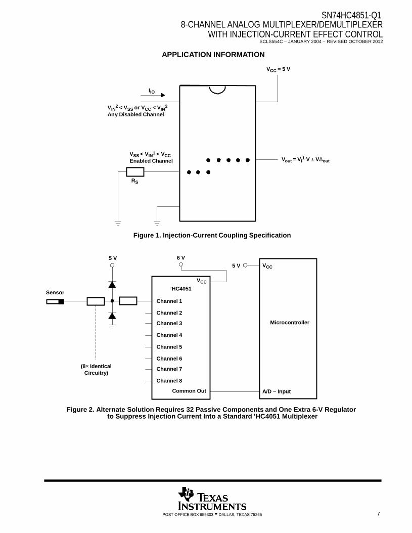
APPLICATION INFORMATION
VCC = 5 V
IIO
VIN
2 < VSS or VCC < VIN2
Any Disabled Channel
VSS < VIN1 < VCC Enabled Channel
Vout = VI
1 V ± VΔout
RS
Figure 1. Injection-Current Coupling Specification
5 V 6 V 5 V VCC
Sensor
’HC4051
Channel 1 Channel 2 Channel 3 Channel 4 Channel 5
VCC Microcontroller
(8× Identical Circuitry)
Channel 6 Channel 7 Channel 8
Common Out
A/D − Input
Figure 2. Alternate Solution Requires 32 Passive Components and One Extra 6-V Regulator
to Suppress Injection Current Into a Standard ’HC4051 Multiplexer
SN74HC4851-Q1 8-CHANNEL ANALOG MULTIPLEXER/DEMULTIPLEXER WITH INJECTION-CURRENT EFFECT CONTROL SCLS554C − JANUARY 2004 − REVISED SEPTEMBER 2012
POST OFFICE BOX 655303 • DALLAS, TEXAS 75265 8
APPLICATION INFORMATION
5 V VCC
Sensor
’HC4851
Channel 1 Channel 2 Channel 3 Channel 4 Channel 5
VCC Microcontroller
(8× Identical Circuitry)
Channel 6 Channel 7 Channel 8
Common Out
A/D − Input
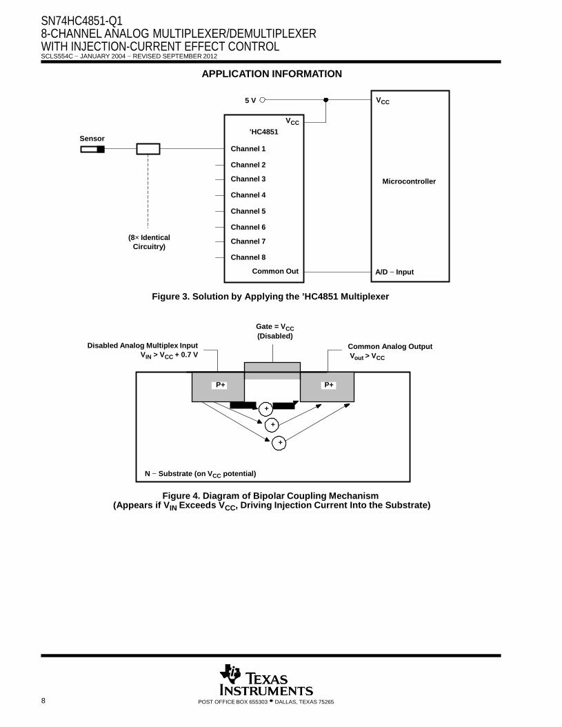
Figure 3. Solution by Applying the ’HC4851 Multiplexer
Disabled Analog Multiplex Input VIN > VCC + 0.7 V
Gate = VCC (Disabled)
Common Analog Output Vout > VCC
P+ P+
+
+
+
N − Substrate (on VCC potential)
Figure 4. Diagram of Bipolar Coupling Mechanism (Appears if VIN Exceeds VCC, Driving Injection Current Into the Substrate)
SN74HC4851-Q1 8-CHANNEL ANALOG MULTIPLEXER/DEMULTIPLEXER
WITH INJECTION-CURRENT EFFECT CONTROL SCLS554C − JANUARY 2004 − REVISED OCTOBER 2012
POST OFFICE BOX 655303 • DALLAS, TEXAS 75265 9
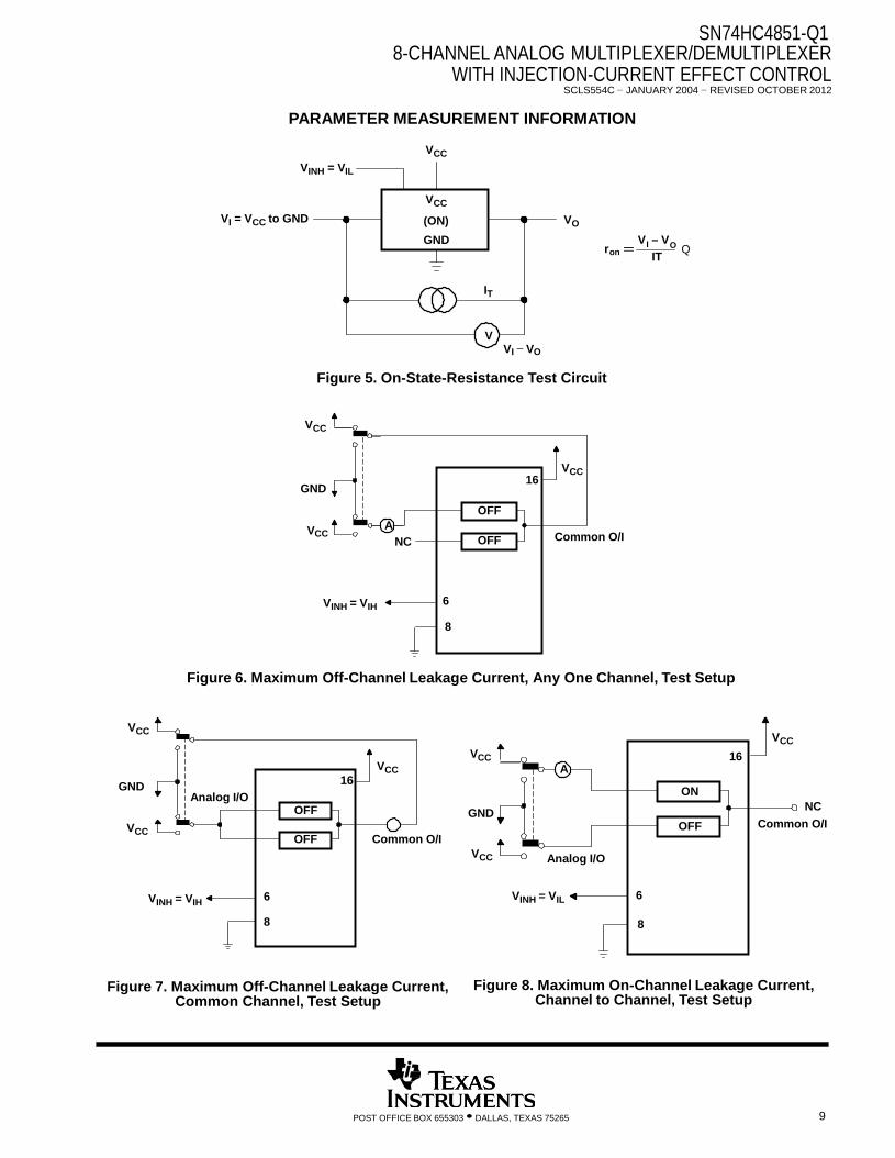
PARAMETER MEASUREMENT INFORMATION
VINH = VIL
VCC
VI = VCC to GND VCC
(ON) GND
VO
ron
=
VI – VO Q IT
IT
V VI − VO
Figure 5. On-State-Resistance Test Circuit
VCC
GND
VCC A
NC
OFF
OFF
VCC 16
Common O/I
VINH = VIH 6
8
Figure 6. Maximum Off-Channel Leakage Current, Any One Channel, Test Setup
VCC
GND
Analog I/O
16 OFF
VCC
VCC
A GND
VCC
16
ON
NC
VCC OFF
Common O/I
VCC
Analog I/O
OFF Common O/I
VINH = VIH 6
8
VINH = VIL 6
8
Figure 7. Maximum Off-Channel Leakage Current, Common Channel, Test Setup
Figure 8. Maximum On-Channel Leakage Current, Channel to Channel, Test Setup
SN74HC4851-Q1 8-CHANNEL ANALOG MULTIPLEXER/DEMULTIPLEXER WITH INJECTION-CURRENT EFFECT CONTROL SCLS554C − JANUARY 2004 − REVISED SEPTEMBER 2012
POST OFFICE BOX 655303 • DALLAS, TEXAS 75265 1
C
C
PARAMETER MEASUREMENT INFORMATION
VCC
Analog I/O
ON/OFF
VCC
16
Common O/I Test
Channel Select
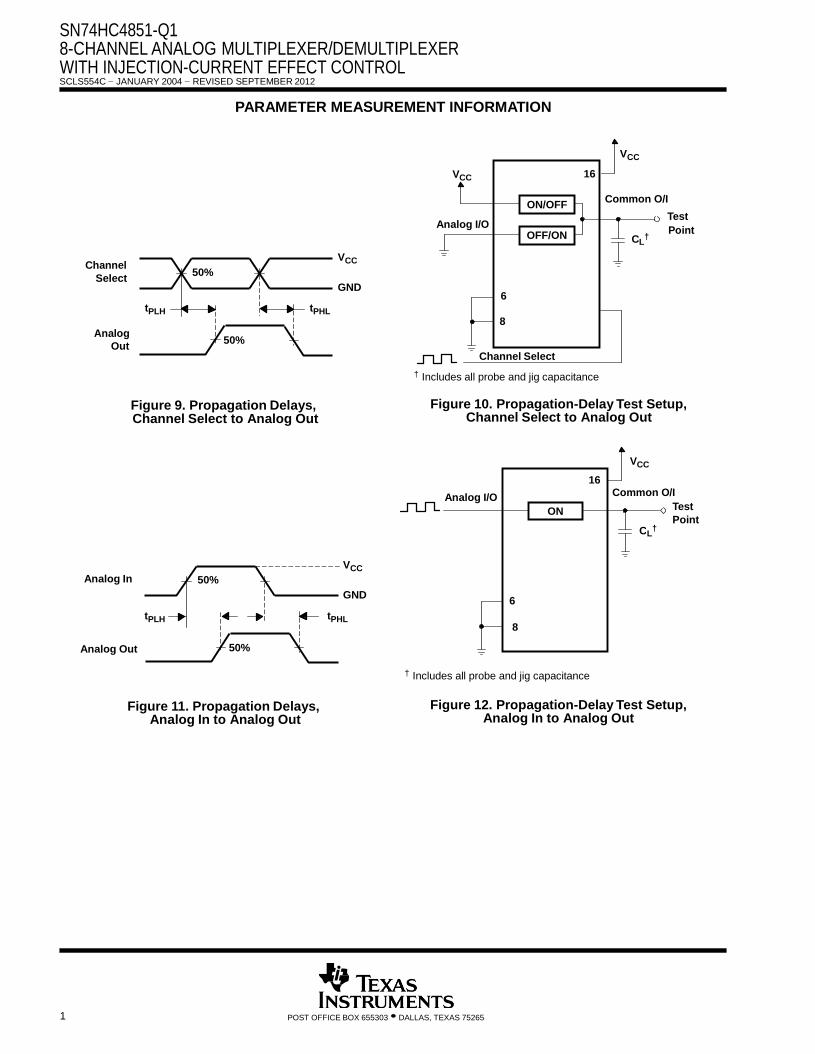
Analog
50% tPLH tPHL
VCC
GND
OFF/ON 6 8
Point † L
Out 50%
Figure 9. Propagation Delays, Channel Select to Analog Out
Channel Select
† Includes all probe and jig capacitance
Figure 10. Propagation-Delay Test Setup, Channel Select to Analog Out
Analog I/O
VCC
16 Common O/I
ON Test Point
† L
Analog In 50%
VCC
GND 6
tPLH tPHL 8
Analog Out 50%
† Includes all probe and jig capacitance
Figure 11. Propagation Delays,
Analog In to Analog Out Figure 12. Propagation-Delay Test Setup,
Analog In to Analog Out
SN74HC4851-Q1 8-CHANNEL ANALOG MULTIPLEXER/DEMULTIPLEXER
WITH INJECTION-CURRENT EFFECT CONTROL SCLS554C − JANUARY 2004 − REVISED OCTOBER 2012
POST OFFICE BOX 655303 • DALLAS, TEXAS 75265 11
C
PARAMETER MEASUREMENT INFORMATION
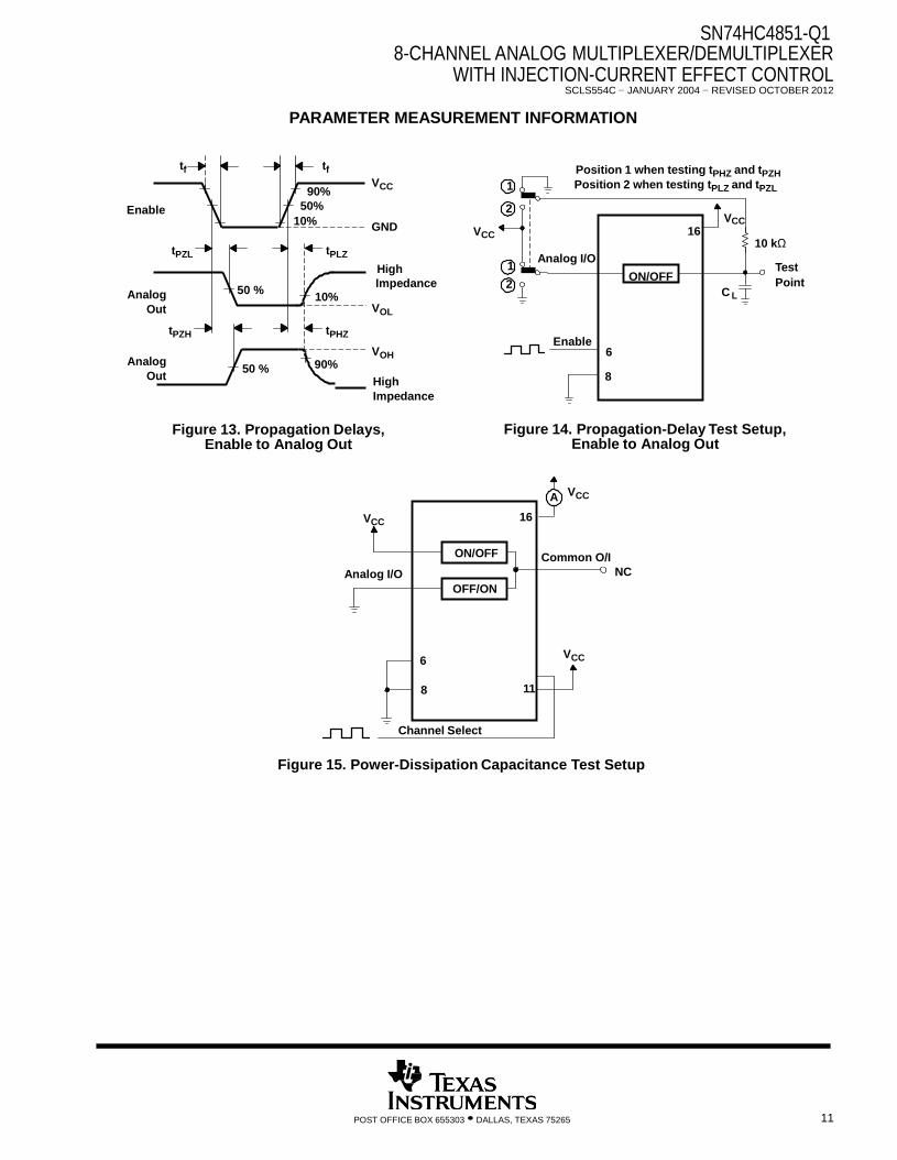
Enable
tf tf
90% 50%
10%
VCC GND
Position 1 when testing tPHZ and tPZH
1 Position 2 when testing tPLZ and tPZL
2 VCC
V tPZL tPLZ
CC 16
Analog I/O 10 kΩ
High 1 ON/OFF Test
Analog
Out
Analog Out
tPZH
50 % 50 %
10%
tPHZ
90%
Impedance VOL VOH High Impedance
2 L
Enable 6
8
Point
Figure 13. Propagation Delays,
Enable to Analog Out Figure 14. Propagation-Delay Test Setup,
Enable to Analog Out
VCC
A VCC
16
ON/OFF Common O/I
Analog I/O NC OFF/ON
6
8 11
VCC
Channel Select
Figure 15. Power-Dissipation Capacitance Test Setup
PACKAGE OPTION ADDENDUM
www.ti.com 11-Apr-2013
Addendum-Page 1
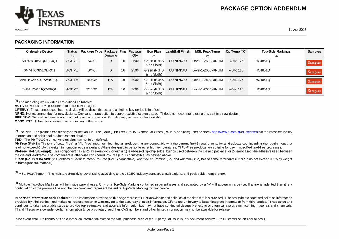
PACKAGING INFORMATION
Orderable Device Status(1)
Package Type PackageDrawing
Pins PackageQty
Eco Plan(2)
Lead/Ball Finish MSL Peak Temp(3)
Op Temp (°C) Top-Side Markings(4)
Samples
SN74HC4851QDRG4Q1 ACTIVE SOIC D 16 2500 Green (RoHS& no Sb/Br)
CU NIPDAU Level-1-260C-UNLIM -40 to 125 HC4851Q
SN74HC4851QDRQ1 ACTIVE SOIC D 16 2500 Green (RoHS& no Sb/Br)
CU NIPDAU Level-1-260C-UNLIM -40 to 125 HC4851Q
SN74HC4851QPWRG4Q1 ACTIVE TSSOP PW 16 2000 Green (RoHS& no Sb/Br)
CU NIPDAU Level-1-260C-UNLIM -40 to 125 HC4851Q
SN74HC4851QPWRQ1 ACTIVE TSSOP PW 16 2000 Green (RoHS& no Sb/Br)
CU NIPDAU Level-1-260C-UNLIM -40 to 125 HC4851Q
(1) The marketing status values are defined as follows:ACTIVE: Product device recommended for new designs.LIFEBUY: TI has announced that the device will be discontinued, and a lifetime-buy period is in effect.NRND: Not recommended for new designs. Device is in production to support existing customers, but TI does not recommend using this part in a new design.PREVIEW: Device has been announced but is not in production. Samples may or may not be available.OBSOLETE: TI has discontinued the production of the device.
(2) Eco Plan - The planned eco-friendly classification: Pb-Free (RoHS), Pb-Free (RoHS Exempt), or Green (RoHS & no Sb/Br) - please check http://www.ti.com/productcontent for the latest availabilityinformation and additional product content details.TBD: The Pb-Free/Green conversion plan has not been defined.Pb-Free (RoHS): TI's terms "Lead-Free" or "Pb-Free" mean semiconductor products that are compatible with the current RoHS requirements for all 6 substances, including the requirement thatlead not exceed 0.1% by weight in homogeneous materials. Where designed to be soldered at high temperatures, TI Pb-Free products are suitable for use in specified lead-free processes.Pb-Free (RoHS Exempt): This component has a RoHS exemption for either 1) lead-based flip-chip solder bumps used between the die and package, or 2) lead-based die adhesive used betweenthe die and leadframe. The component is otherwise considered Pb-Free (RoHS compatible) as defined above.Green (RoHS & no Sb/Br): TI defines "Green" to mean Pb-Free (RoHS compatible), and free of Bromine (Br) and Antimony (Sb) based flame retardants (Br or Sb do not exceed 0.1% by weightin homogeneous material)
(3) MSL, Peak Temp. -- The Moisture Sensitivity Level rating according to the JEDEC industry standard classifications, and peak solder temperature.
(4) Multiple Top-Side Markings will be inside parentheses. Only one Top-Side Marking contained in parentheses and separated by a "~" will appear on a device. If a line is indented then it is acontinuation of the previous line and the two combined represent the entire Top-Side Marking for that device.
Important Information and Disclaimer:The information provided on this page represents TI's knowledge and belief as of the date that it is provided. TI bases its knowledge and belief on informationprovided by third parties, and makes no representation or warranty as to the accuracy of such information. Efforts are underway to better integrate information from third parties. TI has taken andcontinues to take reasonable steps to provide representative and accurate information but may not have conducted destructive testing or chemical analysis on incoming materials and chemicals.TI and TI suppliers consider certain information to be proprietary, and thus CAS numbers and other limited information may not be available for release.
In no event shall TI's liability arising out of such information exceed the total purchase price of the TI part(s) at issue in this document sold by TI to Customer on an annual basis.

PACKAGE OPTION ADDENDUM
www.ti.com 11-Apr-2013
Addendum-Page 2
OTHER QUALIFIED VERSIONS OF SN74HC4851-Q1 :
• Catalog: SN74HC4851
NOTE: Qualified Version Definitions:
• Catalog - TI's standard catalog product
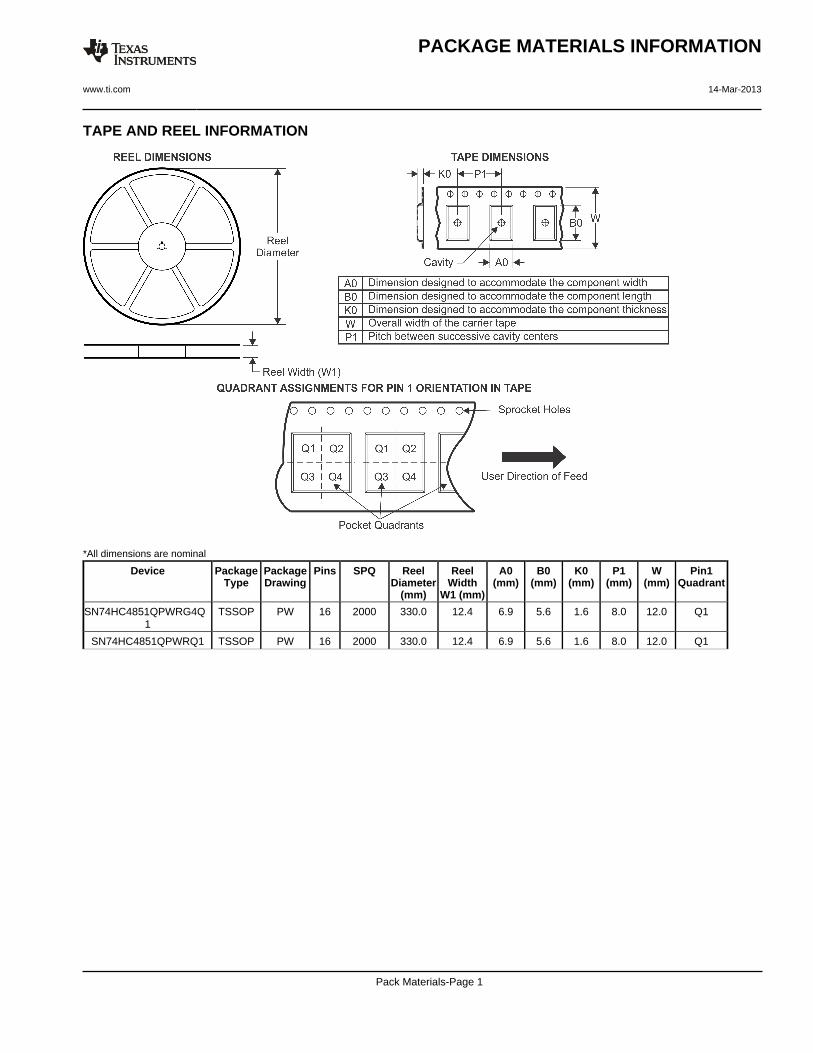
TAPE AND REEL INFORMATION
*All dimensions are nominal
Device PackageType
PackageDrawing
Pins SPQ ReelDiameter
(mm)
ReelWidth
W1 (mm)
A0(mm)
B0(mm)
K0(mm)
P1(mm)
W(mm)
Pin1Quadrant
SN74HC4851QPWRG4Q1
TSSOP PW 16 2000 330.0 12.4 6.9 5.6 1.6 8.0 12.0 Q1
SN74HC4851QPWRQ1 TSSOP PW 16 2000 330.0 12.4 6.9 5.6 1.6 8.0 12.0 Q1
PACKAGE MATERIALS INFORMATION
www.ti.com 14-Mar-2013
Pack Materials-Page 1
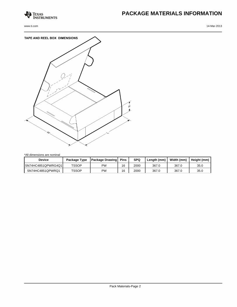
*All dimensions are nominal
Device Package Type Package Drawing Pins SPQ Length (mm) Width (mm) Height (mm)
SN74HC4851QPWRG4Q1 TSSOP PW 16 2000 367.0 367.0 35.0
SN74HC4851QPWRQ1 TSSOP PW 16 2000 367.0 367.0 35.0
PACKAGE MATERIALS INFORMATION
www.ti.com 14-Mar-2013
Pack Materials-Page 2
IMPORTANT NOTICE
Texas Instruments Incorporated and its subsidiaries (TI) reserve the right to make corrections, enhancements, improvements and otherchanges to its semiconductor products and services per JESD46, latest issue, and to discontinue any product or service per JESD48, latestissue. Buyers should obtain the latest relevant information before placing orders and should verify that such information is current andcomplete. All semiconductor products (also referred to herein as “components”) are sold subject to TI’s terms and conditions of salesupplied at the time of order acknowledgment.TI warrants performance of its components to the specifications applicable at the time of sale, in accordance with the warranty in TI’s termsand conditions of sale of semiconductor products. Testing and other quality control techniques are used to the extent TI deems necessaryto support this warranty. Except where mandated by applicable law, testing of all parameters of each component is not necessarilyperformed.TI assumes no liability for applications assistance or the design of Buyers’ products. Buyers are responsible for their products andapplications using TI components. To minimize the risks associated with Buyers’ products and applications, Buyers should provideadequate design and operating safeguards.TI does not warrant or represent that any license, either express or implied, is granted under any patent right, copyright, mask work right, orother intellectual property right relating to any combination, machine, or process in which TI components or services are used. Informationpublished by TI regarding third-party products or services does not constitute a license to use such products or services or a warranty orendorsement thereof. Use of such information may require a license from a third party under the patents or other intellectual property of thethird party, or a license from TI under the patents or other intellectual property of TI.Reproduction of significant portions of TI information in TI data books or data sheets is permissible only if reproduction is without alterationand is accompanied by all associated warranties, conditions, limitations, and notices. TI is not responsible or liable for such altereddocumentation. Information of third parties may be subject to additional restrictions.Resale of TI components or services with statements different from or beyond the parameters stated by TI for that component or servicevoids all express and any implied warranties for the associated TI component or service and is an unfair and deceptive business practice.TI is not responsible or liable for any such statements.Buyer acknowledges and agrees that it is solely responsible for compliance with all legal, regulatory and safety-related requirementsconcerning its products, and any use of TI components in its applications, notwithstanding any applications-related information or supportthat may be provided by TI. Buyer represents and agrees that it has all the necessary expertise to create and implement safeguards whichanticipate dangerous consequences of failures, monitor failures and their consequences, lessen the likelihood of failures that might causeharm and take appropriate remedial actions. Buyer will fully indemnify TI and its representatives against any damages arising out of the useof any TI components in safety-critical applications.In some cases, TI components may be promoted specifically to facilitate safety-related applications. With such components, TI’s goal is tohelp enable customers to design and create their own end-product solutions that meet applicable functional safety standards andrequirements. Nonetheless, such components are subject to these terms.No TI components are authorized for use in FDA Class III (or similar life-critical medical equipment) unless authorized officers of the partieshave executed a special agreement specifically governing such use.Only those TI components which TI has specifically designated as military grade or “enhanced plastic” are designed and intended for use inmilitary/aerospace applications or environments. Buyer acknowledges and agrees that any military or aerospace use of TI componentswhich have not been so designated is solely at the Buyer's risk, and that Buyer is solely responsible for compliance with all legal andregulatory requirements in connection with such use.TI has specifically designated certain components as meeting ISO/TS16949 requirements, mainly for automotive use. In any case of use ofnon-designated products, TI will not be responsible for any failure to meet ISO/TS16949.
Products ApplicationsAudio www.ti.com/audio Automotive and Transportation www.ti.com/automotiveAmplifiers amplifier.ti.com Communications and Telecom www.ti.com/communicationsData Converters dataconverter.ti.com Computers and Peripherals www.ti.com/computersDLP® Products www.dlp.com Consumer Electronics www.ti.com/consumer-appsDSP dsp.ti.com Energy and Lighting www.ti.com/energyClocks and Timers www.ti.com/clocks Industrial www.ti.com/industrialInterface interface.ti.com Medical www.ti.com/medicalLogic logic.ti.com Security www.ti.com/securityPower Mgmt power.ti.com Space, Avionics and Defense www.ti.com/space-avionics-defenseMicrocontrollers microcontroller.ti.com Video and Imaging www.ti.com/videoRFID www.ti-rfid.comOMAP Applications Processors www.ti.com/omap TI E2E Community e2e.ti.comWireless Connectivity www.ti.com/wirelessconnectivity
Mailing Address: Texas Instruments, Post Office Box 655303, Dallas, Texas 75265Copyright © 2015, Texas Instruments Incorporated