Embed Size (px)
Citation preview
610 JOURNAL OF MICROELECTROMECHANICAL SYSTEMS, VOL. 23, NO. 3, JUNE 2014
A Feedback Controlled MEMS Nanopositionerfor On-Chip High-Speed AFM
Ali Mohammadi, Student Member, IEEE, Anthony G. Fowler, Student Member, IEEE,Yuen K. Yong, Member, IEEE, and S. O. Reza Moheimani, Fellow, IEEE
Abstract— We report the design of a two-degree-of-freedommicroelectromechanical systems nanopositioner for on-chipatomic force microscopy (AFM). The device is fabricated usinga silicon-on-insulator-based process to function as the scanningstage of a miniaturized AFM. It is a highly resonant system withits lateral resonance frequency at ∼850 Hz. The incorporatedelectrostatic actuators achieve a travel range of 16 µm in eachdirection. Lateral displacements of the scan table are measuredusing a pair of electrothermal position sensors. These sensors areused, together with a positive position feedback controller, in afeedback loop, to damp the highly resonant dynamics of the stage.The feedback controlled nanopositioner is used, successfully,to generate high-quality AFM images at scan rates as fast as100 Hz. [2013-0063]
Index Terms— Nanopositioning, MEMS, electrothermal sensor,on-chip, AFM.
I. INTRODUCTION
ANANOPOSITIONER is a mechanical device that iscapable of producing repeatable, high-precision motion
with nanometer resolution. This is an invaluable quality inmany areas of micro and nanotechnology, with this type ofmotion commonly being required by processes that involvethe positioning, manipulation and interrogation of samples in arange of micro-scale applications, including molecular biology,nanoassembly, and optical alignment systems [1]–[4].
There has recently been increasing interest in the develop-ment of novel nanopositioning devices that are based on micro-electromechanical systems (MEMS) fabrication processes[5]–[8]. These miniaturized nanopositioners potentially holda number of advantages over conventional macro-sizednanopositioners. Characteristics such as increased operatingbandwidths, lower unit manufacturing costs, simpler bulkfabrication and a much smaller packaged size [5], [9] meanthat MEMS-based nanopositioners represent an attractivesolution for many applications. These attributes have beenexploited in recent high-density probe-based data storage
Manuscript received March 6, 2013; revised June 20, 2013; acceptedOctober 7, 2013. Date of publication December 5, 2013; date of currentversion May 29, 2014. This work was supported in part by the AustralianResearch Council and in part by The University of Newcastle. Subject EditorA. M. Shkel.
The authors are with the School of Electrical Engineering andComputer Science, The University of Newcastle, Callaghan, N.S.W. 2308,Australia (e-mail: [email protected]; [email protected];[email protected]; [email protected]).
Color versions of one or more of the figures in this paper are availableonline at http://ieeexplore.ieee.org.
Digital Object Identifier 10.1109/JMEMS.2013.2287506
devices, in which MEMS nanopositioners are featured as afundamental component of the system [10]–[12].
Recent MEMS nanopositioners have also implemented feed-back control techniques to improve the static and dynamicperformance of the fabricated system. As shown in [13], [14]a closed-loop control system can be used to achieve a higherpositioning accuracy and alleviate imperfections inherent inthe microactuator such as drift and vibrations.
One of the most important tools used in science andengineering in recent times is the atomic force microscope(AFM) [15]. The AFM features a sharp probe of a fewnanometers wide, and is used to interrogate sample surfacesdown to the atomic scale. The use of a MEMS-based nanopo-sitioner as the scanning stage of an AFM greatly reducesthe size of one of the main components of the system.This represents an important step towards the developmentof miniaturized, mass-produced AFMs that represent a fully-integrated, low-cost solution for on-chip scanning. Such aMEMS-based AFM scanner was demonstrated in [16], where a2-degree-of-freedom (DOF) MEMS nanopositioner fabricatedusing a commercial silicon-on-insulator (SOI) process wasused in place of the existing scanning stage for an off-the-shelfAFM. The nanopositioner’s stage contained a series of 3 μmgold features that were used to represent a scan sample, andan open-loop scan of the features was successfully performedby the AFM in tapping mode.
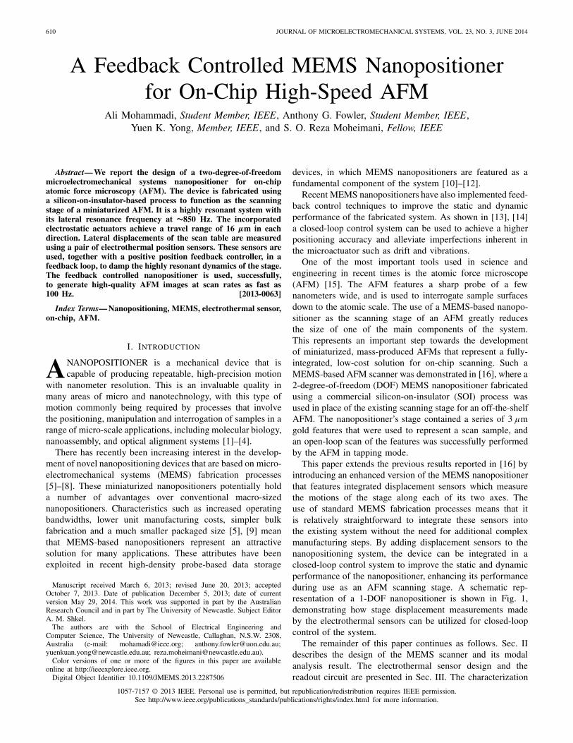
This paper extends the previous results reported in [16] byintroducing an enhanced version of the MEMS nanopositionerthat features integrated displacement sensors which measurethe motions of the stage along each of its two axes. Theuse of standard MEMS fabrication processes means that itis relatively straightforward to integrate these sensors intothe existing system without the need for additional complexmanufacturing steps. By adding displacement sensors to thenanopositioning system, the device can be integrated in aclosed-loop control system to improve the static and dynamicperformance of the nanopositioner, enhancing its performanceduring use as an AFM scanning stage. A schematic rep-resentation of a 1-DOF nanopositioner is shown in Fig. 1,demonstrating how stage displacement measurements madeby the electrothermal sensors can be utilized for closed-loopcontrol of the system.
The remainder of this paper continues as follows. Sec. IIdescribes the design of the MEMS scanner and its modalanalysis result. The electrothermal sensor design and thereadout circuit are presented in Sec. III. The characterization
1057-7157 © 2013 IEEE. Personal use is permitted, but republication/redistribution requires IEEE permission.See http://www.ieee.org/publications_standards/publications/rights/index.html for more information.
MOHAMMADI et al.: FEEDBACK CONTROLLED MEMS NANOPOSITIONER 611
Fig. 1. A schematic diagram of a 1-DOF nanopositioner with electrostaticactuators and electrothermal sensors in a closed-loop control system.
of the device, which includes sensor sensitivity and frequencyresponse measurements, and static non-linearity linearizationof the nanopositioner, is discussed in Sec. IV. Sec. V presentsthe design and implementation of controllers to suppressresonant modes of the device and to facilitate good trackingof reference signals. Sec. VI evaluates the performance of theMEMS nanopositioner for AFM imaging. Sec. VII concludesthe paper.
II. MEMS SCANNER DESIGN
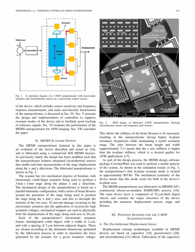
The MEMS nanopositioner featured in this paper isan evolution of the device described and tested in [16],and is fabricated using a commercial SOI MEMS process.As previously stated, the design has been modified such thatthe nanopositioner features integrated electrothermal sensorsthat enable real-time measurements of the stage displacementalong the x and y directions. The fabricated nanopositioner isshown in Fig. 2.
The scanner has two mechanical degrees of freedom, withelectrostatic comb-finger actuators being used to position a3 mm × 3 mm stage along the planar x and y directions.The mechanical design of the nanopositioner is based on aparallel-kinematic configuration, with a series of beam flexuresaround the perimeter of the stage being used to positionthe stage along the x and y axes, and also to decouple themotions of the two axes. To prevent damage occurring to theelectrostatic actuators due the application of excessively highactuation voltages, mechanical stoppers are used to physicallylimit the displacement of the stage along each axis to 20 μm.
Each of the nanopostioner’s electrostatic actuatorsfeature interdigitated comb fingers with a width of 2 μm,and with a spacing of 2 μm between adjacent fingers. Theseare chosen according to the minimum dimensions permittedby the fabrication process in order to maximize the forcegenerated by the actuator for a given actuation voltage.
Fig. 2. SEM images of fabricated 2-DOF nanopositioner, showingelectrothermal sensors and integrated gold features.
This allows the stiffness of the beam flexures to be increased,resulting in the nanopositioner having higher in-planeresonance frequencies while maintaining a useful actuationrange. The ratio between the beam height and width(approximately 7:1) means that the z axis stiffness is higherthan the in-plane stiffness, which is a desired quality forAFM applications [17].
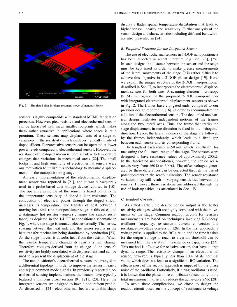
As part of the design process, the MEMS design softwarepackage CoventorWare was used to perform a modal analysisof the system. As shown in the simulation results in Fig. 3,the nanopositioner’s first in-plane resonant mode is locatedat approximately 903 Hz. The mechanical symmetry of thedevice means that this mode exists for both of the device’sin-plane axes.
The MEMS nanopositioner was fabricated via MEMSCAP’scommercial silicon-on-insulator SOIMUMPs process [18].The main device layer is comprised of 25 μm-thick dopedsilicon, and contains the major structures of the deviceincluding the actuators, displacement sensors, stage, andflexures.
III. POSITION SENSORS FOR THE 2-DOFNANOPOSITIONER
A. The Electrothermal Displacement Sensor
Displacement sensing technologies available in MEMSdevices are based on capacitive [19], piezoresistive [20],and electrothermal [21] effects. Fabrication of the capacitive
612 JOURNAL OF MICROELECTROMECHANICAL SYSTEMS, VOL. 23, NO. 3, JUNE 2014
Fig. 3. Simulated first in-plane resonant mode of nanopositioner.
sensors is highly compatible with standard MEMS fabricationprocesses. However, piezoresistive and electrothermal sensorscan be fabricated with much smaller footprints, which makesthem rather attractive in applications where space is at apremium. These sensors map displacements of a stage tovariations in the resistivity of a transducer, typically made ofdoped silicon. Piezoresistive sensors can be operated at lowerpower levels compared to electrothermal sensors. However, theresistance of the doped silicon is more sensitive to temperaturechanges than variations in mechanical stress [22]. The smallfootprint and high sensitivity of electrothermal sensors wereour motivation to utilize this technology to measure displace-ments of the nanopositioning stage.
An early implementation of the electrothermal displace-ment sensor was reported in [21], and it was subsequentlyused in a probe-based data storage device reported in [10].The operating principle of the sensor is based on utilizingthe temperature sensitivity of doped silicon resistance. Theconduction of electrical power through the doped siliconincreases its temperature. The transfer of heat between amoving heat sink (the nanopositioner stage in this case) anda stationary hot resistor (sensor) changes the sensor resis-tance, as depicted in the 1-DOF nanopositioner schematic inFig. 1, where the stage is actuated electrostatically. The narrowspacing between the heat sink and the sensor results in theheat transfer mechanism being dominated by conduction [23].As the stage moves, it absorbs heat from the resistor. Whenthe resistor temperature changes its resistivity will change.Therefore, voltages derived from the change of the sensor’sresistivity are highly correlated with displacement, and can beused to represent the displacement of the stage.
The nanopositioner’s electrothermal sensors are arranged ina differential topology, in order to improve the sensor linearityand reject common mode signals. In previously reported elec-trothermal sensing implementations, the heaters have typicallyfeatured a uniform cross section [9], [21], [23]. Here, theintegrated sensors are designed to have a nonuniform profile.As discussed in [24], electrothermal heaters with this shape
display a flatter spatial temperature distribution that leads tohigher sensor linearity and sensitivity. Further analysis of thesensor design and characteristics including drift and bandwidthare also presented in [24].
B. Proposed Structure for the Integrated Sensor
The use of electrothermal sensors in 1-DOF nanopositionershas been reported in recent literature, e.g. see [23], [25].In such designs the distance between the sensor and the stagemust be kept fixed in order to make precise measurementsof the lateral movements of the stage. It is rather difficult toachieve this objective in a 2-DOF planar design [19]. Here,we exploit the unique structure of the 2-DOF nanopositioner,described in Sec. II, to incorporate the electrothermal displace-ment sensors for both axes. A scanning electron microscope(SEM) micrograph of the proposed 2-DOF nanopositionerwith integrated electrothermal displacement sensors is shownin Fig. 2. The frames have elongated ends, compared to ourprevious design reported in [16], in order to accommodate theaddition of the electrothermal sensors. The decoupled mechan-ical design facilitates independent motions of the framesalong the two lateral axes. Thus, the frame that tracks thestage displacement in one direction is fixed in the orthogonaldirection. Hence, the lateral motions of the stage are followedby the frames independently, which leads to a fixed gapbetween each sensor and its corresponding frame.
The length of each sensor is 50 μm, which is sufficient formeasuring the full travel range of the stage. The sensors weredesigned to have resistance values of approximately 200 �.In the fabricated nanopositioner, however, the sensor resis-tances vary from 160 � to 300 �. The offset voltages gener-ated by these differences can be corrected through the use ofpotentiometers in the readout circuitry. The sensor resistancevariations may still result in varying sensitivities between thesensors. However, these variations are addressed through theuse of look-up tables, as articulated in Sec. IV.
C. Readout Circuitry
As stated earlier, the desired sensor output is the heaterresistivity changes, which are highly correlated with the move-ments of the stage. Common readout circuits for resistivemeasurements are based on techniques involving RC-decay,oscillator frequency, resistance-to-current conversion andresistance-to-voltage conversion [26]. In the first approach, avoltage pulse is applied to the RC circuit, and the time it takesfor the output voltage to reach to a certain threshold can bemeasured from the variation in resistance or capacitance [27].This method is effective for resistive sensors that have a largedynamic range. The resistivity change in an electrothermalsensor, however, is typically less than 10% of its nominalvalue, which does not lead to a significant RC variation. Theeffectiveness of the second approach is impeded by the phasenoise of the oscillator. Particularly, if a ring oscillator is used,it is known that the phase noise contributes substantially to thetotal measurement noise and reduces the achievable SNR [28].
To avoid these complications, we chose to design thereadout circuit based on the concept of resistance-to-voltage

MOHAMMADI et al.: FEEDBACK CONTROLLED MEMS NANOPOSITIONER 613
Fig. 4. Readout circuit schematics: a) Wheatstone bridge. b) TA.
conversion, which uses a Wheatstone bridge, and resistance-to-current conversion, which uses transimpedance ampli-fiers (TA). Both methods were implemented and tested on theMEMS nanopositioner. The Wheatstone bridge is commonlyused in resistive readout circuits. However, it turns out that foridentical resistive changes, a TA-based read out circuit offersa higher sensitivity.
The readout circuits corresponding to the two methodsare schematically illustrated in Fig. 4. The actuation voltage,represented by Va , drives the electrostatic actuator. Vh is thedc heating voltage, RM E M S1,2 are the sensor heated resistorsand Rr1,2, RF1,2 are the bridge reference and the TA feedbackresistors, respectively. The sensor resistance variations can bedescribed as
RM E M S1,2 = R ± δR, (1)
where R is the MEMS resistor value with the stage atthe middle (no displacement) and δR is the resistancechanges associated with the stage displacement. Assuming thatRr1 = Rr2 = Rre f , the bridge output voltage is
Vout B = A2Rre f δR
(R + Rre f )2 Vh, (2)
where A is the differential amplifier voltage gain and Vh isthe bias voltage, which heats the sensors. The balanced bridgeconditions lead to R = Rr1,2. Therefore, the total gain can beobtained as
Vout B
δR= AVh
2R. (3)
Similarly, the output voltage for the TA circuit is given by
VoutT = A2RFδR
(R2 − δR2)Vh (4)
Fig. 5. Comparison of bridge and TA sensitivity.
Fig. 6. Sensor sensitivity curves achieved by the same setup over fouriterations using (a) the Wheatstone bridge and (b) the TA circuit.
As long as no voltage gain is expected from the TA, wemay assume R = RF1,2. Therefore, neglecting δR2, the totalgain can be approximated as:
VoutT
δR= 2AVh
R(5)
Comparing Eqs. (3) and (5) we note that the achievablesensitivity with the TA readout circuit is four times higherthan with the bridge circuit. This is supported by experimentalresults, illustrated in Fig. 5, where for the same actuationvoltage, a larger output voltage is obtained with the TA circuit.In particular, we note from this figure that the slope of theTA readout circuit transfer characteristic, i.e. its sensitivity,is much larger than that of the bridge circuit. Additionally,in the TA topology the heating voltage across the resistoris kept fixed, which leads to a constant voltage mode oper-ation. In contrast, the bridge topology does not guaranteea constant voltage across the resistor. The curves shown inFig. 6(a) are four iterations of the same measurement using the
614 JOURNAL OF MICROELECTROMECHANICAL SYSTEMS, VOL. 23, NO. 3, JUNE 2014
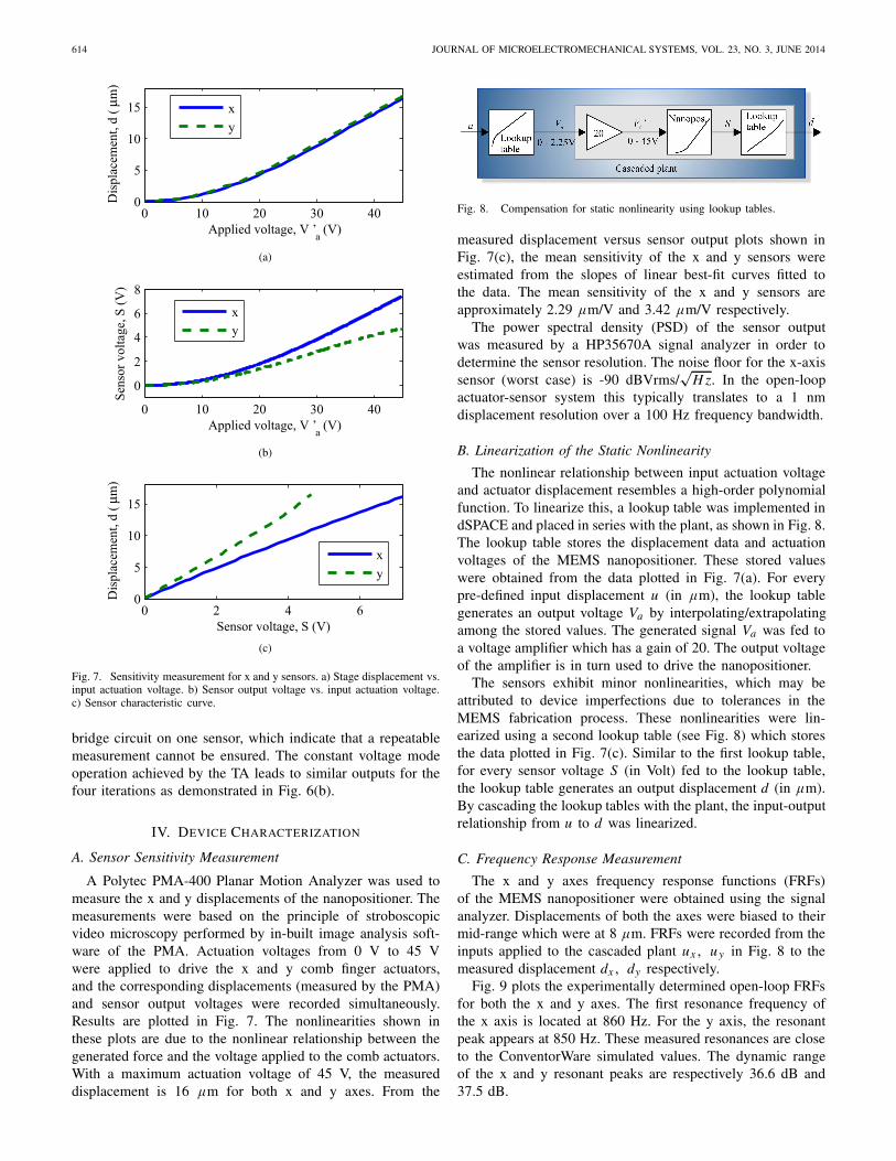
Fig. 7. Sensitivity measurement for x and y sensors. a) Stage displacement vs.input actuation voltage. b) Sensor output voltage vs. input actuation voltage.c) Sensor characteristic curve.
bridge circuit on one sensor, which indicate that a repeatablemeasurement cannot be ensured. The constant voltage modeoperation achieved by the TA leads to similar outputs for thefour iterations as demonstrated in Fig. 6(b).
IV. DEVICE CHARACTERIZATION
A. Sensor Sensitivity Measurement
A Polytec PMA-400 Planar Motion Analyzer was used tomeasure the x and y displacements of the nanopositioner. Themeasurements were based on the principle of stroboscopicvideo microscopy performed by in-built image analysis soft-ware of the PMA. Actuation voltages from 0 V to 45 Vwere applied to drive the x and y comb finger actuators,and the corresponding displacements (measured by the PMA)and sensor output voltages were recorded simultaneously.Results are plotted in Fig. 7. The nonlinearities shown inthese plots are due to the nonlinear relationship between thegenerated force and the voltage applied to the comb actuators.With a maximum actuation voltage of 45 V, the measureddisplacement is 16 μm for both x and y axes. From the
Fig. 8. Compensation for static nonlinearity using lookup tables.
measured displacement versus sensor output plots shown inFig. 7(c), the mean sensitivity of the x and y sensors wereestimated from the slopes of linear best-fit curves fitted tothe data. The mean sensitivity of the x and y sensors areapproximately 2.29 μm/V and 3.42 μm/V respectively.
The power spectral density (PSD) of the sensor outputwas measured by a HP35670A signal analyzer in order todetermine the sensor resolution. The noise floor for the x-axissensor (worst case) is -90 dBVrms/
√H z. In the open-loop
actuator-sensor system this typically translates to a 1 nmdisplacement resolution over a 100 Hz frequency bandwidth.
B. Linearization of the Static Nonlinearity
The nonlinear relationship between input actuation voltageand actuator displacement resembles a high-order polynomialfunction. To linearize this, a lookup table was implemented indSPACE and placed in series with the plant, as shown in Fig. 8.The lookup table stores the displacement data and actuationvoltages of the MEMS nanopositioner. These stored valueswere obtained from the data plotted in Fig. 7(a). For everypre-defined input displacement u (in μm), the lookup tablegenerates an output voltage Va by interpolating/extrapolatingamong the stored values. The generated signal Va was fed toa voltage amplifier which has a gain of 20. The output voltageof the amplifier is in turn used to drive the nanopositioner.
The sensors exhibit minor nonlinearities, which may beattributed to device imperfections due to tolerances in theMEMS fabrication process. These nonlinearities were lin-earized using a second lookup table (see Fig. 8) which storesthe data plotted in Fig. 7(c). Similar to the first lookup table,for every sensor voltage S (in Volt) fed to the lookup table,the lookup table generates an output displacement d (in μm).By cascading the lookup tables with the plant, the input-outputrelationship from u to d was linearized.
C. Frequency Response Measurement
The x and y axes frequency response functions (FRFs)of the MEMS nanopositioner were obtained using the signalanalyzer. Displacements of both the axes were biased to theirmid-range which were at 8 μm. FRFs were recorded from theinputs applied to the cascaded plant ux , uy in Fig. 8 to themeasured displacement dx , dy respectively.
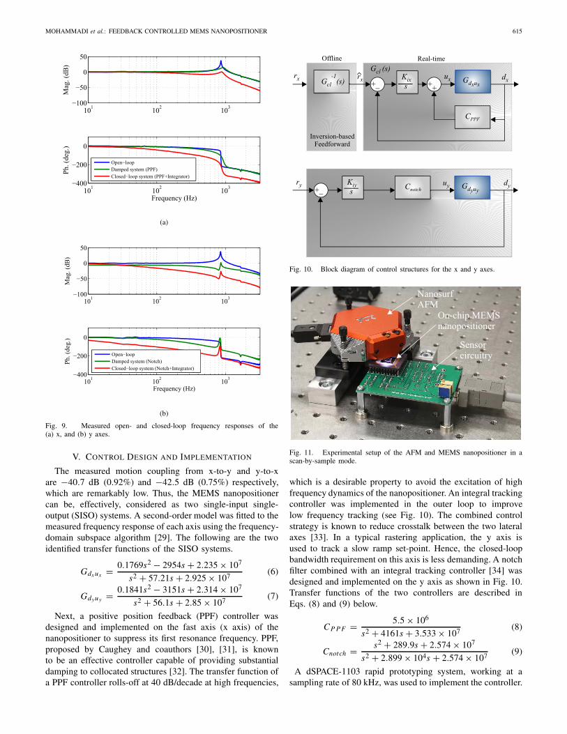
Fig. 9 plots the experimentally determined open-loop FRFsfor both the x and y axes. The first resonance frequency ofthe x axis is located at 860 Hz. For the y axis, the resonantpeak appears at 850 Hz. These measured resonances are closeto the ConventorWare simulated values. The dynamic rangeof the x and y resonant peaks are respectively 36.6 dB and37.5 dB.
MOHAMMADI et al.: FEEDBACK CONTROLLED MEMS NANOPOSITIONER 615
Fig. 9. Measured open- and closed-loop frequency responses of the(a) x, and (b) y axes.
V. CONTROL DESIGN AND IMPLEMENTATION
The measured motion coupling from x-to-y and y-to-xare −40.7 dB (0.92%) and −42.5 dB (0.75%) respectively,which are remarkably low. Thus, the MEMS nanopositionercan be, effectively, considered as two single-input single-output (SISO) systems. A second-order model was fitted to themeasured frequency response of each axis using the frequency-domain subspace algorithm [29]. The following are the twoidentified transfer functions of the SISO systems.
Gdx ux = 0.1769s2 − 2954s + 2.235 × 10⁷
s2 + 57.21s + 2.925 × 10⁷ (6)
Gdyuy = 0.1841s2 − 3151s + 2.314 × 10⁷
s2 + 56.1s + 2.85 × 10⁷ (7)
Next, a positive position feedback (PPF) controller wasdesigned and implemented on the fast axis (x axis) of thenanopositioner to suppress its first resonance frequency. PPF,proposed by Caughey and coauthors [30], [31], is knownto be an effective controller capable of providing substantialdamping to collocated structures [32]. The transfer function ofa PPF controller rolls-off at 40 dB/decade at high frequencies,
Fig. 10. Block diagram of control structures for the x and y axes.
Fig. 11. Experimental setup of the AFM and MEMS nanopositioner in ascan-by-sample mode.
which is a desirable property to avoid the excitation of highfrequency dynamics of the nanopositioner. An integral trackingcontroller was implemented in the outer loop to improvelow frequency tracking (see Fig. 10). The combined controlstrategy is known to reduce crosstalk between the two lateralaxes [33]. In a typical rastering application, the y axis isused to track a slow ramp set-point. Hence, the closed-loopbandwidth requirement on this axis is less demanding. A notchfilter combined with an integral tracking controller [34] wasdesigned and implemented on the y axis as shown in Fig. 10.Transfer functions of the two controllers are described inEqs. (8) and (9) below.
CP P F = 5.5 × 10⁶
s2 + 4161s + 3.533 × 10⁷ (8)
Cnotch = s2 + 289.9s + 2.574 × 10⁷
s2 + 2.899 × 10⁴s + 2.574 × 10⁷ (9)
A dSPACE-1103 rapid prototyping system, working at asampling rate of 80 kHz, was used to implement the controller.
616 JOURNAL OF MICROELECTROMECHANICAL SYSTEMS, VOL. 23, NO. 3, JUNE 2014
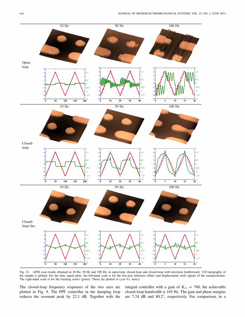
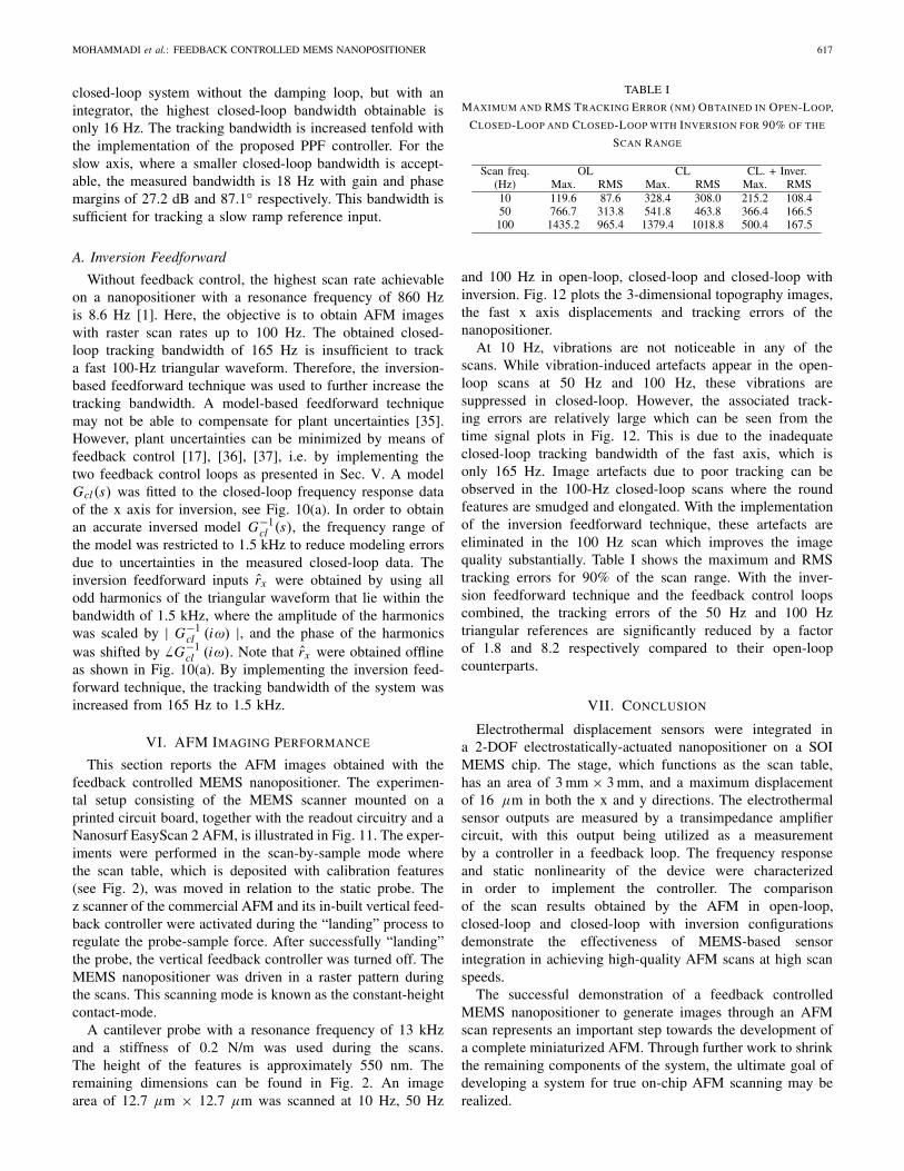
Fig. 12. AFM scan results obtained at 10 Hz, 50 Hz and 100 Hz, in open-loop, closed-loop and closed-loop with inversion feedforward. 3-D topography ofthe sample is plotted. For the time signal plots, the left-hand scale is for the fast-axis reference (blue) and displacement (red) signals of the nanopositioner.The right-hand scale is for the tracking errors (green). These are plotted in (μm Vs. msec).
The closed-loop frequency responses of the two axes areplotted in Fig. 9. The PPF controller in the damping loopreduces the resonant peak by 22.1 dB. Together with the
integral controller with a gain of Kix = 700, the achievableclosed-loop bandwidth is 165 Hz. The gain and phase marginsare 7.24 dB and 80.2◦, respectively. For comparison, in a
MOHAMMADI et al.: FEEDBACK CONTROLLED MEMS NANOPOSITIONER 617
closed-loop system without the damping loop, but with anintegrator, the highest closed-loop bandwidth obtainable isonly 16 Hz. The tracking bandwidth is increased tenfold withthe implementation of the proposed PPF controller. For theslow axis, where a smaller closed-loop bandwidth is accept-able, the measured bandwidth is 18 Hz with gain and phasemargins of 27.2 dB and 87.1◦ respectively. This bandwidth issufficient for tracking a slow ramp reference input.
A. Inversion Feedforward
Without feedback control, the highest scan rate achievableon a nanopositioner with a resonance frequency of 860 Hzis 8.6 Hz [1]. Here, the objective is to obtain AFM imageswith raster scan rates up to 100 Hz. The obtained closed-loop tracking bandwidth of 165 Hz is insufficient to tracka fast 100-Hz triangular waveform. Therefore, the inversion-based feedforward technique was used to further increase thetracking bandwidth. A model-based feedforward techniquemay not be able to compensate for plant uncertainties [35].However, plant uncertainties can be minimized by means offeedback control [17], [36], [37], i.e. by implementing thetwo feedback control loops as presented in Sec. V. A modelGcl(s) was fitted to the closed-loop frequency response dataof the x axis for inversion, see Fig. 10(a). In order to obtainan accurate inversed model G−1
cl (s), the frequency range ofthe model was restricted to 1.5 kHz to reduce modeling errorsdue to uncertainties in the measured closed-loop data. Theinversion feedforward inputs r̂x were obtained by using allodd harmonics of the triangular waveform that lie within thebandwidth of 1.5 kHz, where the amplitude of the harmonicswas scaled by | G−1
cl (iω) |, and the phase of the harmonicswas shifted by � G−1
cl (iω). Note that r̂x were obtained offlineas shown in Fig. 10(a). By implementing the inversion feed-forward technique, the tracking bandwidth of the system wasincreased from 165 Hz to 1.5 kHz.
VI. AFM IMAGING PERFORMANCE
This section reports the AFM images obtained with thefeedback controlled MEMS nanopositioner. The experimen-tal setup consisting of the MEMS scanner mounted on aprinted circuit board, together with the readout circuitry and aNanosurf EasyScan 2 AFM, is illustrated in Fig. 11. The exper-iments were performed in the scan-by-sample mode wherethe scan table, which is deposited with calibration features(see Fig. 2), was moved in relation to the static probe. Thez scanner of the commercial AFM and its in-built vertical feed-back controller were activated during the “landing” process toregulate the probe-sample force. After successfully “landing”the probe, the vertical feedback controller was turned off. TheMEMS nanopositioner was driven in a raster pattern duringthe scans. This scanning mode is known as the constant-heightcontact-mode.
A cantilever probe with a resonance frequency of 13 kHzand a stiffness of 0.2 N/m was used during the scans.The height of the features is approximately 550 nm. Theremaining dimensions can be found in Fig. 2. An imagearea of 12.7 μm × 12.7 μm was scanned at 10 Hz, 50 Hz
TABLE I
MAXIMUM AND RMS TRACKING ERROR (NM) OBTAINED IN OPEN-LOOP,
CLOSED-LOOP AND CLOSED-LOOP WITH INVERSION FOR 90% OF THE
SCAN RANGE
and 100 Hz in open-loop, closed-loop and closed-loop withinversion. Fig. 12 plots the 3-dimensional topography images,the fast x axis displacements and tracking errors of thenanopositioner.
At 10 Hz, vibrations are not noticeable in any of thescans. While vibration-induced artefacts appear in the open-loop scans at 50 Hz and 100 Hz, these vibrations aresuppressed in closed-loop. However, the associated track-ing errors are relatively large which can be seen from thetime signal plots in Fig. 12. This is due to the inadequateclosed-loop tracking bandwidth of the fast axis, which isonly 165 Hz. Image artefacts due to poor tracking can beobserved in the 100-Hz closed-loop scans where the roundfeatures are smudged and elongated. With the implementationof the inversion feedforward technique, these artefacts areeliminated in the 100 Hz scan which improves the imagequality substantially. Table I shows the maximum and RMStracking errors for 90% of the scan range. With the inver-sion feedforward technique and the feedback control loopscombined, the tracking errors of the 50 Hz and 100 Hztriangular references are significantly reduced by a factorof 1.8 and 8.2 respectively compared to their open-loopcounterparts.
VII. CONCLUSION
Electrothermal displacement sensors were integrated ina 2-DOF electrostatically-actuated nanopositioner on a SOIMEMS chip. The stage, which functions as the scan table,has an area of 3 mm × 3 mm, and a maximum displacementof 16 μm in both the x and y directions. The electrothermalsensor outputs are measured by a transimpedance amplifiercircuit, with this output being utilized as a measurementby a controller in a feedback loop. The frequency responseand static nonlinearity of the device were characterizedin order to implement the controller. The comparisonof the scan results obtained by the AFM in open-loop,closed-loop and closed-loop with inversion configurationsdemonstrate the effectiveness of MEMS-based sensorintegration in achieving high-quality AFM scans at high scanspeeds.
The successful demonstration of a feedback controlledMEMS nanopositioner to generate images through an AFMscan represents an important step towards the development ofa complete miniaturized AFM. Through further work to shrinkthe remaining components of the system, the ultimate goal ofdeveloping a system for true on-chip AFM scanning may berealized.
618 JOURNAL OF MICROELECTROMECHANICAL SYSTEMS, VOL. 23, NO. 3, JUNE 2014
ACKNOWLEDGMENT
The research was performed in the Laboratory for Dynamicsand Control of Nanosystems at The University of Newcastle.The authors would like to acknowledge the support of theAustralian Research Council. Some of the SEM images wereobtained with the assistance of the Electron Microscope andX-Ray Unit of the University of Newcastle.
REFERENCES
[1] S. Devasia, E. Eleftheriou, and S. O. R. Moheimani, “A survey of controlissues in nanopositioning,” IEEE Trans. Control Syst. Technol., vol. 15,no. 5, pp. 802–823, Sep. 2007.
[2] J. Shi, J. Dertouzos, A. Gafni, and D. Steel, “Application of single-molecule spectroscopy in studying enzyme kinetics and mechanism,”in Fluorescence Spectroscopy (Methods in Enzymology), vol. 450,L. Brand and M. L. Johnson, Eds. New York, NY, USA: Academic,2008, pp. 129–157.
[3] J. J. Gorman, Y. S. Kim, A. E. Vladár, and N. G. Dagalakis, “Designof an on-chip microscale nanoassembly system,” Int. J. Control, vol. 1,no. 6, pp. 710–721, 2007.
[4] J. J. Gorman, N. G. Dagalakis, and B. G. Boone, “Multi-loop controlof a nanopositioning mechanism for ultra-precision beam steering,”Proc. SPIE, vol. 5160, pp. 170–181, Aug. 2003.
[5] S. Bergna, J. Gorman, and N. Dagalakis, “Design and modeling ofthermally actuated MEMS nanopositioners,” in Proc. ASME IMECE,2005, pp. 561–568.
[6] J. J. Gorman, Y. S. Kim, and N. G. Dagalakis, “Control of MEMSnanopositioners with nano-scale resolution,” in Proc. ASME IMECE,Nov. 2006, pp. 1–9.
[7] D. Brouwer, B. de Jong, and H. Soemers, “Design and modeling of a sixDOFs MEMS-based precision manipulator,” Precis. Eng., vol. 34, no. 2,pp. 307–319, Apr. 2010.
[8] G. Brown, L. Li, R. Bauer, J. Liu, and D. Uttamchandani, “A two-axishybrid MEMS scanner incorporating electrothermal and electrostaticactuators,” in Proc. Int. Conf. Opt. MEMS Nanophoton., Aug. 2010,pp. 115–116.
[9] Y. Zhu, A. Bazaei, S. O. R. Moheimani, and M. R. Yuce, “Design,modeling, and control of a micromachined nanopositioner with inte-grated electrothermal actuation and sensing,” J. Microelectromech. Syst.,vol. 20, no. 3, pp. 711–719, Jun. 2011.
[10] M. A. Lantz, H. E. Rothuizen, U. Drechsler, W. Haberle, andM. Despont, “A vibration resistant nanopositioner for mobile parallel-probe storage applications,” J. Microelectromech. Syst., vol. 16, no. 1,pp. 130–139, Feb. 2007.
[11] A. Pantazi, A. Sebastian, G. Cherubini, M. Lantz, H. Pozidis,H. Rothuizen, et al., “Control of MEMS-based scanning-probe data-storage devices,” IEEE Trans. Control Syst. Technol., vol. 15, no. 5,pp. 824–841, Sep. 2007.
[12] J. Engelen, M. Lantz, H. Rothuizen, L. Abelmann, and M. Elwenspoek,“Improved performance of large stroke comb-drive actuators by usinga stepped finger shape,” in Proc. Int. Solid-State Sensors, Actuat.Microsyst. Conf., Jun. 2009, pp. 1762–1765.
[13] B. Koo, X. Zhang, J. Dong, S. M. Salapaka, and P. M. Ferreira,“A 2 degree-of-freedom SOI-MEMS translation stage with closed-looppositioning,” J. Microelectromech. Syst., vol. 21, no. 1, pp. 13–22,Feb. 2012.
[14] J. Ouyang and Y. Zhu, “Z-shaped MEMS thermal actuators: Piezore-sistive self-sensing and preliminary results for feedback control,”J. Microelectromech. Syst., vol. 21, no. 3, pp. 596–604, Jun. 2012.
[15] G. Binnig, C. F. Quate, and C. Gerber, “Atomic force microscope,” Phys.Rev. Lett., vol. 56, no. 9, pp. 930–933, 1986.
[16] A. G. Fowler, A. N. Laskovski, A. C. Hammond, andS. O. R. Moheimani, “A 2-DOF electrostatically actuated MEMSnanopositioner for on-chip AFM,” J. Microelectromech. Syst., vol. 21,no. 4, pp. 771–773, Aug. 2012.
[17] Y. K. Yong, S. O. R. Moheimani, B. J. Kenton, and K. K. Leang, “Invitedreview article: High-speed flexure-guided nanopositioning: Mechani-cal design and control issues,” Rev. Sci. Instrum., vol. 83, no. 12,pp. 121101-1–121101-22, 2012.
[18] A. Cowen, G. Hames, D. Monk, S. Wilcenski, and B. Hardy, SOI-MUMPs Design Handbook. Durham, NC, USA: MEMSCAP Inc., 2011.
[19] L. Ji, Y. Zhu, S. O. R. Moheimani, and M. R. Yuce, “A micromachined2 DOF nanopositioner with integrated capacitive displacement sensor,”in Proc. IEEE Sensors, Nov. 2010, pp. 1464–1467.
[20] R. Messenger, Q. Aten, T. McLain, and L. Howell, “Piezoresistivefeedback control of a MEMS thermal actuator,” J. Microelectromech.Syst., vol. 18, no. 6, pp. 1267–1278, Dec. 2009.
[21] M. A. Lantz, G. K. Binnig, M. Despont, and U. Drechsler, “A micro-mechanical thermal displacement sensor with nanometer resolution,”Scientific, vol. 16, no. 8, pp. 1089–1094, 2005.
[22] A. Barlian, W.-T. Park, J. Mallon, A. Rastegar, and B. Pruitt, “Review:Semiconductor piezoresistance for microsystems,” Proc. IEEE, vol. 97,no. 3, pp. 513–552, Mar. 2009.
[23] B. Krijnen, R. P. Hogervorst, J. W. van Dijk, J. B. C. Engelen,L. A. Woldering, D. M. Brouwer, et al., “A single-mask thermaldisplacement sensor in MEMS,” J. Micromech. Microeng., vol. 21, no. 7,pp. 74007–074018, 2011.
[24] A. G. Fowler, A. Bazaei, and S. O. R. Moheimani, “Design and analysisof nonuniformly shaped heaters for improved MEMS-based electrother-mal displacement sensing,” J. Microelectromech. Syst., vol. 22, no. 3,pp. 687–694, Jun. 2013.
[25] Y. Zhu, S. O. R. Moheimani, and M. R. Yuce, “Simultaneous capacitiveand electrothermal position sensing in a micromachined nanopositioner,”IEEE Electron Device Lett., vol. 32, no. 8, pp. 1146–1148, Aug. 2011.
[26] K. Blake, “An990: Analog sensor conditioning circuits—An overview,”Microchip Technology Inc., Chandler, AZ, USA, Tech. Rep., 2005.
[27] J. Lu, M. Inerowicz, S. Joo, J. K. Kwon, and B. Jung, “A low-power,wide-dynamic-range semi-digital universal sensor readout circuit usingpulsewidth modulation,” IEEE Sensors J., vol. 11, no. 5, pp. 1134–1144,May 2011.
[28] A. Mohammadi, M. R. Yuce, and S. O. R. Moheimani, “Frequencymodulation technique for MEMS resistive sensing,” IEEE Sensors J.,vol. 12, no. 8, pp. 2690–2698, Aug. 2012.
[29] T. McKelvey, H. Akcay, and L. Ljung, “Subspace based multivariablesystem identification from frequency response data,” IEEE Trans. Autom.Control, vol. 41, no. 7, pp. 960–978, Jul. 1996.
[30] C. J. Goh and T. K. Caughey, “On the stability problem caused by finiteactuator dynamics in the collocated control of large space structures,”Int. J. Control, vol. 41, no. 3, pp. 787–802, 1985.
[31] J. L. Fanson and T. K. Caughey, “Positive position feedback control forlarge space structures,” AIAA J., vol. 28, no. 4, pp. 717–724, 1990.
[32] S. O. R. Moheimani, B. J. G. Vautier, and B. Bhikkaji, “Experimentalimplementation of extended multivariable PPF control on an active struc-ture,” IEEE Trans. Control Syst. Technol., vol. 14, no. 3, pp. 443–455,May 2006.
[33] I. A. Mahmood and S. O. R. Moheimani, “Making a commercial AFMmore accurate and faster using positive position feedback control,” Rev.Sci. Instrum., vol. 80, no. 6, pp. 063705-1–063705-8, 2009.
[34] K. K. Leang and S. Devasia, “Feedforward control of piezoactuatorsin atomic force microscope systems: Inversion-based compensation fordynamics and hysteresis,” IEEE Trans. Control Syst. Technol., vol. 15,no. 5, pp. 927–935, Sep. 2007.
[35] Y. Zhao and S. Jayasuriya, “Feedforward controllers and trackingaccuracy in the presence of plant uncertainty,” ASME J. Dyn. Syst.,Meas., Control, vol. 117, no. 4, pp. 490–495, 1995.
[36] S. S. Aphale, S. Devasia, and S. O. R. Moheimani, “High-bandwidthcontrol of a piezoelectric nanopositioning stage in the present of plantuncertainties,” Nanotechnology, vol. 19, no. 12, pp. 125503-1–125503-9,2008.
[37] K. K. Leang, Q. Zou, and S. Devasia, “Feedforward control of piezoactu-ators in atomic force microscope systems: Inversion-based compensationfor dynamics and hysteresis,” IEEE Control Syst. Mag., vol. 29, no. 1,pp. 70–82, Feb. 2009.
Ali Mohammadi (S’09) received the B.Sc. andM.Sc. degrees in electrical and electronics engineer-ing from Urmia University, Urmia, Iran, and theIran University of Science and Technology, Tehran,Iran, in 2003 and 2007, respectively. He is currentlypursuing the Ph.D. degree with the University ofNewcastle, Australia where he has been awardedan Endeavour International Postgraduate ResearchScholarship. His previous research involves data-converters and frequency synthesizers for telecom-munication systems. His current research interests
include MEMS sensors with special focus on the interface circuit design.
MOHAMMADI et al.: FEEDBACK CONTROLLED MEMS NANOPOSITIONER 619
Anthony G. Fowler (S’10) was born in Taree,Australia. He received the Bachelor’s degree in elec-trical engineering from The University of Newcastle,Callaghan, Australia, in 2010. He is the recipient ofan Australian Postgraduate Award, and is currentlypursuing the Ph.D. degree in electrical engineeringat the same university.
His research interests include the design and analy-sis of novel MEMS devices for energy harvestingand nanopositioning applications.
Yuen K. Yong (M’09) received the B.Eng. degree(1st Class Honors) in mechatronic engineering andthe Ph.D. degree in mechanical engineering fromThe University of Adelaide, Adelaide, Australia,in 2001 and 2007, respectively. She is currentlyan Australian Research Council DECRA Fellowwith the School of Electrical Engineering and Com-puter Science, The University of Newcastle. Herresearch interests include the design and control ofnanopositioning systems, high-speed atomic forcemicroscopy, finite-element analysis of smart mate-
rials and structures, and sensing and actuation.Dr. Yong was a recipient of the 2008 IEEE/ASME International Conference
on Advanced Intelligent Mechatronics (AIM) Best Conference Paper FinalistAward. She is a member of the Technical Program Committee of AIM and theInternational Conference on Manipulation, Manufacturing, and Measurementon the Nanoscale (3M-NANO). She is also an associate editor of theInternational Journal of Advanced Robotic Systems.
S. O. Reza Moheimani (F’11) received hisundergraduate degree in electrical engineeringfrom Shiraz University in 1991 and completed hisdoctoral studies at the University of New SouthWales, Australia, in 1996. In 1997 he joined TheUniversity of Newcastle, Australia, embarking ona new research program addressing the dynamicsand control design issues related to high-precisionmechatronic systems. Professor Moheimani is thefounder and director of the Laboratory for Dynamicsand Control of Nanosystems, a multimillion-dollar
state-of-the-art research facility. His current research interests are mainly inthe area of ultrahigh-precision mechatronic systems, with particular emphasison dynamics and control at the nanometer scale, including applications ofcontrol and estimation in nanopositioning systems for high-speed scanningprobe microscopy, modeling and control of microcantilever-based devices,control of microactuators in microelectromechanical systems, and design,modelling and control of micromachined nanopositioners for on-chip atomicforce microscopy.
His work has been recognised by a number of awards including theIFAC Nathaniel B. Nichols Medal (2014); IFAC Mechatronic SystemsAward (2013); IEEE Control Systems Technology Award (2009); AustralianResearch Council Future Fellowship (2009); IEEE TRANSACTIONS ON
CONTROL SYSTEMS TECHNOLOGY Outstanding Paper Award (2007);Australian Research Council Postdoctoral Fellowship (1999); and severalbest student paper awards in various conferences. He has served on theeditorial boards of a number of journals, including the IEEE/ASMETRANSACTIONS ON MECHATRONICS, IEEE TRANSACTIONS ON CONTROLSYSTEMS TECHNOLOGY, and Control Engineering Practice. He haschaired several international conferences and workshops and currentlychairs the IFAC Technical Committee on Mechatronic Systems. Hehas published over 270 refereed papers and five books and editedvolumes. He is a Fellow of IEEE, IFAC and Institute of Physics (UK).


![Liquid Encapsulation Technology for Microelectromechanical ... · Liquid Encapsulation Technology for Microelectromechanical Systems Norihisa Miki ... [27]. Therefore, sealing with](https://img.dokumen.tips/doc/110x75/5ebd6745ad290220a7044b42/liquid-encapsulation-technology-for-microelectromechanical-liquid-encapsulation.jpg)