Embed Size (px)
Citation preview

DRV
D/STVCC
LEB S/OCP
TSD
PWM OSC
REG
FB
15.5 V/ 8.9 V
DMAX 75%
28.5 V
7.8 V
GND
FM/ELP
160 μA
RS Q
S QR
7.1 V
SlopeCompensation
Drain PeakCurrentCompensation
VREG
STARTUP
Istartup=1.6 mA
S2 Q
CKS1
R
OLP
tOLP=tFM×32
FrequencyModulation
RQS
UVLO
ELP
RST
7.1 V
OVP
FeedbackControl
OCP12 V
STR-W6252D
DescriptionThe STR-W6200D series are current-mode PWM ICs that incorporate controller chips. These devices are manufactured using a proprietary high-voltage BCD process, and avalanche-guaranteed MOSFETs. These elements allow power supply systems designs that are highly reliable and simple, with fewer peripheral components. These ICs also provide Auto-Burst mode operation, which lowers input power requirements at light loads, and improves efficiency over the entire load range and universal-input range.
Applicatons include:
▪ TV set top box▪ LCD PC monitor, LCD TV▪ Printer, scanner▪ General consumer, PC, and industrial applications
requiring SMPS power supply with standby mode
Features and Benefits▪ Overcurrent protection (OCP) with ac input voltage
compensation function; no additional peripheral circuits required—minimizes dependency of OCP on ac input
▪ Overload protection (OLP) with integrated timer reduces power stress (temperature rise) at overload condition, requires no peripheral components
▪ Avalanche-guaranteed MOSFET improves device capability of withstanding excess surge voltage, providing a simple surge absorber circuit without breakdown voltage derating
▪ Start-up circuit eliminates the need for a start-up resistor, and helps to reduce input power consumption
60 W-Universal Input/40 W-230 Vac InputPWM Switching Regulators
Functional Block Diagram
Package: TO-220
Not to scale
Continued on the next page…
28103.52
60 W-Universal Input/40 W-230 Vac InputPWM Switching RegulatorsSTR-W6252D
2Allegro MicroSystems, Inc.115 Northeast Cutoff, Box 15036Worcester, Massachusetts 01615-0036 (508) 853-5000www.allegromicro.com
▪ Bias Assist function improves start-up performance by self-
biasing the VCC pin, and allows a use of a small value VCC
capacitor, resulting in improved response to overvoltage
conditions
▪ Very low current consumption in nonoperating (UVLO) state:
ICC(off) = 5 μA (typical) at VCC = 13.8 V
▪ Slope compensation circuit stabilizes operation, preventing
interference from subharmonics
▪ Leading Edge Blanking
▪ Various protections:• Overcurrent Protection (OCP), pulse-by-pulse sensing• Overload Protection (OLP), auto restart after certain duration• External Latch Protection (ELP), latched• Overvoltage Protection (OVP), latched• Thermal Shut Down (TSD), latched
▪ Externally-activated shut down protection (ELP) for emergency system shut down
▪ Auto-Burst Standby function (pin < 0.1 W at zero output load condition)
▪ Audible noise reducing function in Standby mode▪ TO-220 full-molded package with 6 pins
Features and Benefits (continued)
Selection GuidePart Number PackingSTRW6252D 50 pieces per tube
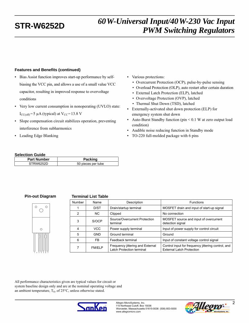
Pin-out Diagram
All performance characteristics given are typical values for circuit or system baseline design only and are at the nominal operating voltage and an ambient temperature, TA, of 25°C, unless oth er wise stated.
Terminal List TableNumber Name Description Functions
1 D/ST Drain/startup terminal MOSFET drain and input of start-up signal
2 NC Clipped No connection
3 S/OCP Source/Overcurrent Protection terminal
MOSFET source and input of overcurrent detection signal
4 VCC Power supply terminal Input of power supply for control circuit
5 GND Ground terminal Ground
6 FB Feedback terminal Input of constant voltage control signal
7 FM/ELP Frequency jittering and External Latch Protection terminal
Control input for frequency jittering control, and External Latch Protection
1 2 3 4 5 6 7

60 W-Universal Input/40 W-230 Vac InputPWM Switching RegulatorsSTR-W6252D
3Allegro MicroSystems, Inc.115 Northeast Cutoff, Box 15036Worcester, Massachusetts 01615-0036 (508) 853-5000www.allegromicro.com
ABSOLUTE MAXIMUM RATINGS at TA = 25°CCharacteristic Symbol Terminal Note Rating Unit
Drain Current1 IDpeak 1-3 Single Pulse 3.2 AMaximum Switching Current2 IDMAX 1-3 TA = –20 to 125°C 3.2 A
Single Pulse Avalanche Energy3EAS 1-3 Single Pulse 62 mJ
IDpeak 1-3 VDD = 99 V, L = 20 mH 2.3 AS/OCP Terminal Voltage VOCP 3-5 –6 to 6 VFM/ELP Terminal Voltage VFM 7-5 –0.3 to 12 VFM/ELP Terminal Inflow Current IFM 7-5 3 mAFB Terminal Voltage VFB 6-5 –0.3 to 9 VController (MIC) Input Voltage VCC 4-5 0 to 32 V
MOSFET Power Dissipation4 PD1 8-1With infinite heatsink 26 WWithout heatsink 1.3 W
Controller (MIC) Power Dissipation PD2 5-3 For Vcc×Icc 0.8 WOperating Internal Frame Temperature TF – Refer to TOP –20 to 115 °COperating Ambient Temperature Top – –20 to 115 °CStorage Temperature Tstg – –40 to 125 °CChannel Junction Temperature TJ – 150 °C1Refer to figure 12IDMAX is the drain current on the D/ST pin determined by the drive voltage of the IC and the threshold voltage, Vth, of the MOSFET3Refer to figure 34Refer to figure 4
Temperature, TF (°C)
Safe
Ope
ratin
g Ar
ea
Tem
pera
ture
Der
atin
g C
oeffi
cien
t (%
)
0
20
40
60
80
100
0 25 50 75 100 125 150Drain-to-Source Voltage, VDS (V)
Dra
in C
urre
nt, I
D (A
)
10.00
0.10
1.00
0.01
100.00
10 100 10001
1 ms
0.1 ms
Current lim
it
due to R DS(on)
Refer to figure 1 for MOSFET SOA temperature derating coefficient
Figure 1 – MOSFET Safe Operating AreaDerating Curve
Figure 2 – MOSFET Safe Operating AreaDrain Current versus Voltage
at TA = 25°C, Single Pulse

60 W-Universal Input/40 W-230 Vac InputPWM Switching RegulatorsSTR-W6252D
4Allegro MicroSystems, Inc.115 Northeast Cutoff, Box 15036Worcester, Massachusetts 01615-0036 (508) 853-5000www.allegromicro.com
Channel Junction Temperature, TJ (°C)
EA
S T
empe
ratu
re D
erat
ing
Coe
ffici
ent (
%)
0
20
40
60
80
100
25 50 75 100 125 150Time, t (s)
Tran
sien
t The
rmal
Res
ista
nce,
RJC
(°C
/W)
1.00
0.10
0.01
10.00
100μ10μ 10m1m 100m1μ
Ambient Temperature, TA (°C)
Pow
er D
issi
patio
n, P
D1
(W)
0
5
10
15
20
25
30
0 20 40 60 80 100 120 140 160
PD1 = 1.3 W at TA ≤ 25°CWithout heatsink
With infinite heatsinkPD1 = 26 W at TA ≤ 25°C
Figure 3 – MOSFET Avalanche Energy Derating Curve Figure 4 – Transient Thermal Resistance
Figure 5 – MOSFET Power Dissipation versus Temperature

60 W-Universal Input/40 W-230 Vac InputPWM Switching RegulatorsSTR-W6252D
5Allegro MicroSystems, Inc.115 Northeast Cutoff, Box 15036Worcester, Massachusetts 01615-0036 (508) 853-5000www.allegromicro.com
ELECTRICAL CHARACTERISTICS valid at VCC = 18 V, TA = 25°C, unless otherwise specifiedCharacteristic Symbol Terminal Test Conditions Min. Typ. Max Units
Power Supply Start-up Operation
Operation Start Voltage VCC(ON) 4-5 (VCC voltage at which operation starts) Measurement circuit 1, VCC = 0 through 13.9 through 17.1 V 13.9 15.5 17.1 V
Operation Stop Voltage VCC(OFF) 4-5 (VCC voltage at which operation stops) Measurement circuit 1, VCC = 17.1 through 9.8 to 8.0 V 8.0 8.9 9.8 V
Circuit Current in Operation ICC(ON) 4-5 (Inflow current into VCC terminal in oscillation) Measurement circuit 1 – 1.4 2.8 mA
Circuit Current in Non-Oscillation ICC(STOP) 4-5 (Inflow current into VCC terminal at VFB = 0 V) Measurement circuit 1 – 0.8 1.3 mA
Circuit Current in Non-Operation ICC(OFF) 4-5 (Inflow current into VCC terminal prior to oscillation) Measurement circuit 1, VCC = 13.8 – 5 20 μA
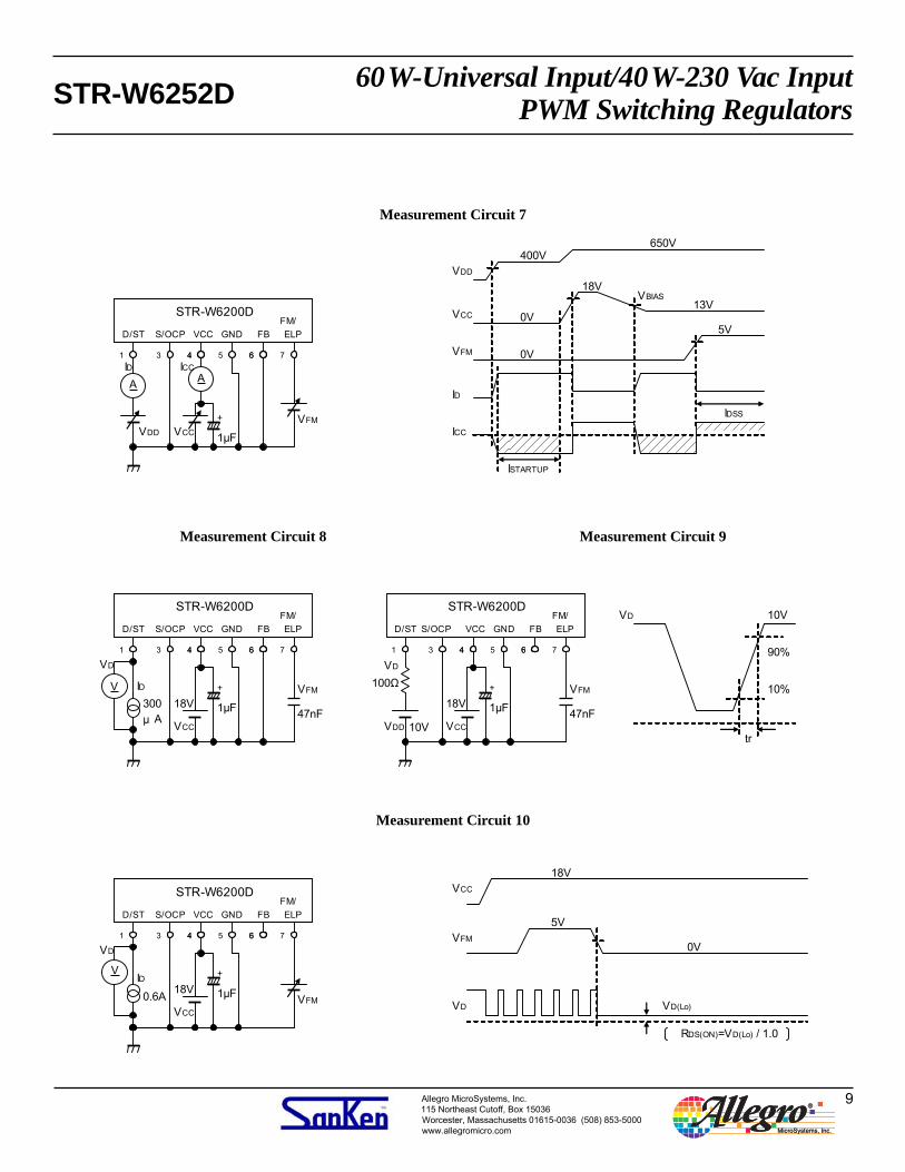
Start-up Current Istartup 4-5 (Inflow current into D/ST terminal) Measurement circuit 7, VCC = 0, D/ST = 450 V –0.9 –1.6 –2.3 mA
Bias Assist Voltage VBIAS 4-5(VCC voltage at which Istartup starts, and IstartupBias begins) Measurement circuit 7, VCC = 17.1 through 13.6 to 16.8 V
13.6 15.2 16.8 V
Operating Characteristics
FM/ELP High Threshold Voltage VFM(H) 7-5 (FM/ELP terminal voltage at which IFM changes from –13 μA to 13 μA) Measurement circuit 2 4.0 4.5 5.0 V
FM/ELP Low Threshold Voltage VFM(L) 7-5 (FM/ELP terminal voltage at which IFM changes from 13 μA to –13 μA) Measurement circuit 2 2.4 2.8 3.2 V
FM/ELP Voltage Hysteresis VFMhys 7-5 (VFM(H) – VFM(L)) Measurement circuit 2 1.4 1.7 1.8 V
FM/ELP Outflow Current1 IFMsrc 7-5 (FM/ELP terminal outflow current at VFM = VFM(L)) Measurement circuit 2 –17.4 –13 –8.6 μA
FM/ELP Inflow Current1 IFMsink 7-5 (FM/ELP terminal inflow current at VFM = VFM(H)) Measurement circuit 2 8.6 13 17.4 μA
Average Switching Frequency fOSC(av) 1-5 (D/ST terminal average oscillation frequency) Measurement circuit 2 60 67 74 kHz
Frequency Jitter Deviation ∆f 1-5 fOSC (peak-to-peak) Measurement circuit 2 4.8 6.9 9 kHz
Maximum Duty Cycle DMAX 1-5 (Maximum width of the low portion of the D/ST terminal waveform) Measurement circuit 2 71 75 79 %
FB Maximum Feedback Current1 IFB(MAX) 6-5 (FB terminal outflow current at VFB = 0 V) Measurement circuit 3 –220 –160 –100 μA
Burst Threshold Voltage Vburst(th) 6-5Set VFM = 0 V and decrease VFB (Vburst(th) is the FB terminal voltage level at which D/ST changes from low to high) Measurement circuit 3
0.99 1.10 1.21 V
Slope Compensation Start-up Duty Cycle DSLP 6-5 DSLP = (t3 / t4) × 100 (see figure for measurement
circuit 4 for values of t) Measurement circuit 4 – 27 – %
Slope Compensation Rate SLP 6-5 SLP = 0.02 / (t2 – t1) (see figure for measurement circuit 4 for values of t) Measurement circuit 4 –22 –17 –12 mV/μs
Continued on next page…

60 W-Universal Input/40 W-230 Vac InputPWM Switching RegulatorsSTR-W6252D
6Allegro MicroSystems, Inc.115 Northeast Cutoff, Box 15036Worcester, Massachusetts 01615-0036 (508) 853-5000www.allegromicro.com
Protection Operation
OCP Threshold Voltage at Zero Duty Cycle (0% On-Duty) VOCP1 3-5
Set VFM = 0 V and increase VOCP. (VOCP1 is the S/OCP terminal voltage level at which D/ST changes from low to high) Measurement circuit 5
0.71 0.78 0.86 V
Drain Peak Current Compensation Coefficient DPC – DPC = –0.75× SLP / fOSC(av) 1.5 1.9 2.3 mV/
DC%
OCP Threshold Voltage After Compensation VOCP2 3-5 VOCP2 = DPC × DMAX + VOCP1 0.82 0.93 1.04 V
Leading Edge Blanking Time tblank 1-5 (The low portion of the D/ST terminal waveform at VOCP = 2 V) Measurement circuit 5 280 400 520 ns
OLP Delay Time tOLP 1-5 (Time between setting FB terminal open and when oscillation stops) Measurement circuit 6 – 200 – ms
Circuit Current in OLP-Operation ICC (OLP) 4-5 (Inflow current into VCC terminal after OLP operation) Measurement circuit 6 – 410 700 μA
OVP Protection Voltage VCC(OVP) 4-5
(VCC terminal voltage at which the voltage of D/ST terminal is switched from low to high by decreasing VFB after setting VFM = 0 V) Measurement circuit 1, VCC = 18.0 V through 27 to 30 V
27 28.5 30 V
Latch Circuit Sustaining Current2 ICC(La.H) 4-5 (Inflow current into VCC terminal after OVP operation) Measurement circuit 1, VCC = 7.8 V – 140 220 μA
Latch Circuit Release Voltage2 VCC(La.OFF) 4-5(VCC voltage at which ICC is dropped below 20 μA by decreasing VCC after OVP operation)VCC = 31.0 V through 7.8 to 6.4 V
6.4 7.1 7.8 V
ELP Threshold Voltage VELP 7-5(FM/ELP terminal voltage at which the oscillation of the D/ST terminal waveform is stopped by increasing VFM) Measurement circuit 2
6.4 7.1 7.8 V
Inflow Current at External Latch Protection IELP 7-5 (Inflow current at VFM = VELP) Measurement circuit 2 – 55 100 μA
Thermal Shut Down Operating Temperature TJTSD – 135 – – °C
Power MOSFET CharacteristicsDrain-to-Source Breakdown Voltage VDSS 1-3 ID = 300 μA, Measurement circuit 8 650 – – V
Drain Leakage Current IDSS 1-3 VD = 650 V, Measurement circuit 7 – – 300 μA
ON-Resistance RDS(ON) 1-3 ID = 1.0 A, VFM = 0 V Measurement circuit 10 – – 2.8 Ω
Switching Time tr 1-3 Measurement circuit 9 – – 400 ns
Thermal Resistance RθJ-F – Measured between junction and internal frame – – 2.04 °C/W
Single Pulse Avalanche Energy EAS – Measurement circuit 11 – – – –1Input and output current polarity at the device pin; plus(+) represents sink and minus(–) represents source.2The latch circuit means a circuit operated ELP, OVP, and TSD.
ELECTRICAL CHARACTERISTICS, continued, valid at VCC = 18 V, TA = 25°C, unless otherwise specifiedCharacteristic Symbol Terminal Test Conditions Min. Typ. Max Units

60 W-Universal Input/40 W-230 Vac InputPWM Switching RegulatorsSTR-W6252D
7Allegro MicroSystems, Inc.115 Northeast Cutoff, Box 15036Worcester, Massachusetts 01615-0036 (508) 853-5000www.allegromicro.com
13.8VVCC(ON)
VCC(OFF)
18V
ICC(OFF)
VCC
VD
ICC
VCCc(La.OFF)8V
ICC(La.H)ICC(STOP)
32V
VD
VFM VFML
VFMH VLFM+(VFMH-VFML)/2
IFM
fosc(av)
t1
Isnk(FM)
fosc(Hi) fosc(Lo)
t2
Δf =f osc(Hi)-f osc(Lo)Dmax= t2/ t1х100
Isrc(FM)
0μA
4.5Vtyp
2.8Vtyp
VELP
1μF
VCC
100ΩA
+ICC
VDD 10V
VD
100Ω
VDD 10V
VD
A
IFM
VFM
18V
1
D/ST S/OCP VCC GND FBFM/ELP
STR-W6200D
3 4 5 6 74 6
1
D/ST S/OCP VCC GND FBFM/ELP
STR-W6200D
3 4 5 6 74 6
100Ω
VDD 10V
VD
A
IFB
VFB
VFM
1
D/ST S/OCP VCC GND FBFM/ELP
STR-W6200D
3 4 5 6 74 6
ICC(ON)
VFB
5V
VFB VFM
VFM
VCC(OVP)
2V
3.65V0V
1μFVCC
+
18V 1μFVCC
+
0V
0V
VCC
18V
VFB 0V
VFB
5V
VFM
VburstVFB
VD
0V
IFB(MAX)
IFB
5V0V
VCC
18V
VOFF(FM)
IELP
5V
0V
2V
Measurement Circuit 1
Measurement Circuit 2
Measurement Circuit 3

60 W-Universal Input/40 W-230 Vac InputPWM Switching RegulatorsSTR-W6252D
8Allegro MicroSystems, Inc.115 Northeast Cutoff, Box 15036Worcester, Massachusetts 01615-0036 (508) 853-5000www.allegromicro.com
Measurement Circuit 4
Measurement Circuit 6
Measurement Circuit 5
VD
VOCP
VOCP1
VD(Lo)
tblank
0V
2V
VFM
VD
ICC
100Ω
VDD 10V
VD
tOLP(= tFM 16)
ICC(OLP)
t FM
D/ST S/OCP VCC GND FBFM/ELP
STR-W6200D
3 4 5 6 74 6
VFM
5V0V
3.65V
1
D/ST S/OCP VCC GND FBFM/ELP
STR-W6200D
3 4 5 6 74 6
VFB
7.8 V typ
VFB
VFM18V 1μFVCC
+VOCP
100
VDD 20V
VD
1
VFM
47nF1μF
VCC
A+
ICC
18V
VCC
18V
VCC
18 V
SW ON OFF
SW
1
D/ST S/OCP VCC GND FBFM/ELP
STR-W6200D
3 4 5 6 74 6
VFB
4V
VFM
18V 1μFVCC
+VOCP
100Ω
VDD 10V
VD
VFB
VD
4V
VOCP
Internal feedback signal
V1-0.04V V1-0.02V
t1 t2
t4
0.68V
VCC
18V
VFM3.65V
5V
t3 t5(≈tblank)DSLP= t3 / t4 100SLP = 0.02 / (t2-t1)
V1
VOCP2 = (–0.75 × SLP × DMAX / fOSC(av)) + VOCP1
60 W-Universal Input/40 W-230 Vac InputPWM Switching RegulatorsSTR-W6252D
9Allegro MicroSystems, Inc.115 Northeast Cutoff, Box 15036Worcester, Massachusetts 01615-0036 (508) 853-5000www.allegromicro.com
10V
90%
10%
tr
VDD
AID
ID
VD
V
1
D/ST S/OCP VCC GND FBFM/ELP
STR-W6200D
3 4 5 6 74 6
1
D/ST S/OCP VCC GND FBFM/ELP
STR-W6200D
3 4 5 6 74 6
VD
100Ω
VDD 10V
VD
1
D/ST S/OCP VCC GND FBFM/ELP
STR-W6200D
3 4 5 6 74 6
RDS(ON)=VD(Lo) / 1.0
1μFVCC
+ VFM
VFM
47nF18V 1μFVCC
+ VFM
47nF18V 1μFVCC
+
VD VD(Lo)
D/ST S/OCP VCC GND FBFM/ELP
STR-W6200D
3 4 5 6 74 6 VFM
5V
0V
VFM18V 1μFVCC
+
1
ID
VD
V
0.6A
VCC
18V
AICC
300μ A
VDD
VCC
ID
650V
13V
IDSS
VFM
18V
5V
VBIAS
0V
0V
400V
ISTARTUP
ICC
Measurement Circuit 7
Measurement Circuit 8 Measurement Circuit 9
Measurement Circuit 10

60 W-Universal Input/40 W-230 Vac InputPWM Switching RegulatorsSTR-W6252D
10Allegro MicroSystems, Inc.115 Northeast Cutoff, Box 15036Worcester, Massachusetts 01615-0036 (508) 853-5000www.allegromicro.com
TYPICAL APPLICATION CIRCUIT
1 4
3 7 5 6
V C CD/ST
FM /ELP
STR -W 6200D
S/O C P
VIIN( ac)
G N D
O UT
G ND
FBOption
Measurement Circuit 11
L
VDS
Vcc 18V
VGS 8V
VDS
IL
VDSpeak
VDD
t
VDD
VGS
1
D/ST S/OCP VCC GND FBFM/ELP
STR-W6200D
3 4 5 6 74 6
18V 1μFVCC
+

60 W-Universal Input/40 W-230 Vac InputPWM Switching RegulatorsSTR-W6252D
11Allegro MicroSystems, Inc.115 Northeast Cutoff, Box 15036Worcester, Massachusetts 01615-0036 (508) 853-5000www.allegromicro.com
PACKAGE DIMENSIONS, TO-220
10.0 ±0.2 4.2 ±0.2
2.8 ±0.2
Ø3.
2 ±0
.2
2.6 ±0.1
(2×R1)
Terminal dimension at case surface
5.08 ±0.6
1.74+0.2–0.1
1.34+0.2–0.1
0.45+0.2–0.1
16.9
±0.
3
10.4
±0.
5
5.0
±0.5
7.9
±0.2
4 ±0
.22.
8 M
AX
(5.4
)
Gate Burr
Branding
XXXXXXXXXXXXXXXX
Gate burr: 0.3 mm (max.)Terminal core material: CuTerminal treatment: Ni plating and solder dipHeat sink material: CuHeat sink treatment: Ni platingLeadform: 2003Weight (approximate): 2.3 g
Dimensions in millimeters
Drawing for reference onlyBranding codes (exact appearance at manufacturer discretion):1st line, type: W62522nd line, lot: YMDD R Where: Y is the last digit of the year of manufacture M is the month (1 to 9, O, N, D) DD is the 2-digit date R is the manufacturer registration symbol
1 2 3 4 5 6 7
Terminal dimensions at case surface6×P1.27 ±0.15 = 7.62 ±0.15
Terminal dimension at lead tips
Leadframe plating Pb-free. Device composition complies with the RoHS directive.

60 W-Universal Input/40 W-230 Vac InputPWM Switching RegulatorsSTR-W6252D
12Allegro MicroSystems, Inc.115 Northeast Cutoff, Box 15036Worcester, Massachusetts 01615-0036 (508) 853-5000www.allegromicro.com
PACKING SPECIFICATIONSMinimum packing option: Tube FM-205 E
Shipping Tube Dimensions:Wall thickness: 0.6±0.3 mmWall warp: <2 mmMaterial: Hardened polyvinylCoating: antistaticTolerance ±0.4 mm, unless otherwise specified
All dimensions: mm
Side marked“ANTISTATIC”
(3.6)
(15.
4)
9 × R0.65.1
2.85
14.3
8.9
35.0
1.4
9.5+0
.3–0
.1
4.8+0.4 0
1.3+0.3–0.2
Shipping Carton Dimensions:Capacity: 1800 pieces maximum per carton 36 tubes per carton 3 rows, 12 tubes per row
Spacer
Carton(side view)
Spacer
Tube
620
125
185
Tube

60 W-Universal Input/40 W-230 Vac InputPWM Switching RegulatorsSTR-W6252D
13Allegro MicroSystems, Inc.115 Northeast Cutoff, Box 15036Worcester, Massachusetts 01615-0036 (508) 853-5000www.allegromicro.com
Because reliability can be affected adversely by improper storage environments and handling methods, please observe the following cautions.Cautions for Storage• Ensure that storage conditions comply with the standard temperature (5°C to 35°C) and the standard relative humidity (around 40 to 75%); avoid
storage locations that experience extreme changes in temperature or humidity.• Avoid locations where dust or harmful gases are present and avoid direct sunlight.• Reinspect for rust in leads and solderability of products that have been stored for a long time.Cautions for Testing and Handling When tests are carried out during inspection testing and other standard test periods, protect the products from power surges from the testing device,
shorts between adjacent products, and shorts to the heatsink.Remarks About Using Silicone Grease with a Heatsink• When silicone grease is used in mounting this product on a heatsink, it shall be applied evenly and thinly. If more silicone grease than required is
applied, it may produce stress.• Volatile-type silicone greases may produce cracks after long periods of time, resulting in reduced heat radiation effect. Silicone grease with low
consistency (hard grease) may cause cracks in the mold resin when screwing the product to a heatsink.• Our recommended silicone greases for heat radiation purposes, which will not cause any adverse effect on the product life, are indicated below:
Type Suppliers
G746 Shin-Etsu Chemical Co., Ltd.
YG6260 Toshiba Silicone Co., Ltd.
SC102 Dow Corning Toray Silicone Co., Ltd.Soldering• When soldering the products, please be sure to minimize the working time, within the following limits: 260±5°C 10 s 350±5°C 3 s• Soldering iron should be at a distance of at least 1.5 mm from the body of the productsElectrostatic Discharge• When handling the products, operator must be grounded. Grounded wrist straps worn should have at least 1 MΩ of resistance to ground to prevent
shock hazard.• Workbenches where the products are handled should be grounded and be provided with conductive table and floor mats.• When using measuring equipment such as a curve tracer, the equipment should be grounded.• When soldering the products, the head of soldering irons or the solder bath must be grounded in other to prevent leak voltages generated by them
from being applied to the products.• The products should always be stored and transported in our shipping containers or conductive containers, or be wrapped in aluminum foil.Assembly• During soldering or other operations, the interior frame temperature of the device should never exceed 105°C.• Recommended screw torque through the mounting tab is 0,588 to 0.785 N • m (6 to 8 kgf • cm)
WARNING — These devices are designed to be operated at lethal voltages and energy levels. Circuit designs that embody these components must conform with applicable safety requirements. Pre cau tions must be taken to prevent accidental contact with power-line potentials. Do not connect ground ed test equipment.
The use of an isolation transformer is recommended during circuit development and breadboarding.

60 W-Universal Input/40 W-230 Vac InputPWM Switching RegulatorsSTR-W6252D
14Allegro MicroSystems, Inc.115 Northeast Cutoff, Box 15036Worcester, Massachusetts 01615-0036 (508) 853-5000www.allegromicro.com
The products described herein are manufactured in Ja pan by Sanken Electric Co., Ltd. for sale by Allegro MicroSystems, Inc. Sanken and Allegro reserve the right to make, from time to time, such de par tures from the detail spec i fi ca tions as may be re quired to per mit im-
prove ments in the per for mance, reliability, or manufacturability of its prod ucts. Therefore, the user is cau tioned to verify that the in for ma tion in this publication is current before placing any order.
When using the products described herein, the ap pli ca bil i ty and suit abil i ty of such products for the intended purpose shall be reviewed at the users responsibility.
Although Sanken undertakes to enhance the quality and reliability of its prod ucts, the occurrence of failure and defect of semi con duc tor products at a certain rate is in ev i ta ble.
Users of Sanken products are requested to take, at their own risk, preventative measures including safety design of the equipment or systems against any possible injury, death, fires or damages to society due to device failure or malfunction.
Sanken products listed in this publication are designed and intended for use as components in general-purpose electronic equip ment or apparatus (home ap pli anc es, office equipment, tele com mu ni ca tion equipment, measuring equipment, etc.). Their use in any application requiring radiation hardness assurance (e.g., aero space equipment) is not supported.
When considering the use of Sanken products in ap pli ca tions where higher reliability is re quired (transportation equipment and its control systems or equip ment, fire- or burglar-alarm systems, various safety devices, etc.), contact a company sales representative to discuss and obtain written confirmation of your spec i fi ca tions.
The use of Sanken products without the written consent of Sanken in applications where ex treme ly high reliability is required (aerospace equip-ment, nuclear power-control stations, life-support systems, etc.) is strictly prohibited.
The information in clud ed herein is believed to be accurate and reliable. Ap pli ca tion and operation examples described in this pub li ca tion are given for reference only and Sanken and Allegro assume no re spon si bil i ty for any in fringe ment of in dus tri al property rights, intellectual property rights, or any other rights of Sanken or Allegro or any third party that may result from its use.
Copyright © 2006-2007 Allegro MicroSystems, Inc.This datasheet is based on Sanken datasheet SSE23677

60 W-Universal Input/40 W-230 Vac InputPWM Switching RegulatorsSTR-W6252D
15Allegro MicroSystems, Inc.115 Northeast Cutoff, Box 15036Worcester, Massachusetts 01615-0036 (508) 853-5000www.allegromicro.com
Asia-PacificChina
Sanken Electric Hong Kong Co., Ltd.Suite 1026, Ocean CentreCanton Road, TsimshatsuiKowloon, Hong KongTel: 852-2735-5262, Fax: 852-2735-5494
Sanken Electric (Shanghai) Co., Ltd.Room 3202, Maxdo CentreXingyi Road 8, Changning DistrictShanghai, ChinaTel: 86-21-5208-1177, Fax: 86-21-5208-1757
Taiwan Sanken Electric Co., Ltd.Room 1801, 18th Floor88 Jung Shiau East Road, Sec. 2Taipei 100, Taiwan R.O.C.Tel: 886-2-2356-8161, Fax: 886-2-2356-8261
JapanSanken Electric Co., Ltd.Overseas Sales HeadquartersMetropolitan Plaza Building1-11-1 Nishi-Ikebukuro, Toshima-kuTokyo 171-0021, JapanTel: 81-3-3986-6164, Fax: 81-3-3986-8637
KoreaSanken Electric Korea Co., Ltd.Samsung Life Yeouido Building 16F23-10, Yeouido-Dong, Yeongdeungpo-guSeoul 150-734, KoreaTel: 82-2-714-3700, Fax: 82-2-3272-2145
SingaporeSanken Electric Singapore Pte. Ltd. 150 Beach Road, #14-03 The Gateway WestSingapore 189720Tel: 65-6291-4755, Fax: 65-6297-1744
EuropeSanken Power Systems (UK) Limited Pencoed Technology ParkPencoed, Bridgend CF35 5HY, United KingdomTel: 44-1656-869-100, Fax: 44-1656-869-162
North AmericaUnited States
Allegro MicroSystems, Inc.115 Northeast CutoffWorcester, Massachusetts 01606, U.S.A.Tel: 1-508-853-5000, Fax: 1-508-853-7895
Allegro MicroSystems, Inc.14 Hughes Street, Suite B105Irvine, California 92618, U.S.A.Tel: 1-949-460-2003, Fax: 1-949-460-7837
Worldwide Contacts