Embed Size (px)
Citation preview
5th Generation Intel® Core™
Processor Family, Intel® Core™ MProcessor Family, Mobile Intel®Pentium® Processor Family, andMobile Intel® Celeron® ProcessorFamilyDatasheet – Volume 1 of 2
June 2015
Order No.: 330834-005v1

You may not use or facilitate the use of this document in connection with any infringement or other legal analysis concerning Intel products describedherein. You agree to grant Intel a non-exclusive, royalty-free license to any patent claim thereafter drafted which includes subject matter disclosedherein.
No license (express or implied, by estoppel or otherwise) to any intellectual property rights is granted by this document.
All information provided here is subject to change without notice. Contact your Intel representative to obtain the latest Intel product specifications androadmaps.
The products described may contain design defects or errors known as errata which may cause the product to deviate from published specifications.Current characterized errata are available on request.
Copies of documents which have an order number and are referenced in this document may be obtained by calling 1-800-548-4725 or visit http://www.intel.com/design/literature.htm.
Intel technologies’ features and benefits depend on system configuration and may require enabled hardware, software or service activation. Learnmore at http://www.intel.com/ or from the OEM or retailer.
No computer system can be absolutely secure.
Intel® Hyper-Threading Technology (Intel® HT Technology) is available on select Intel® Core™ processors. It requires an Intel® HT Technology enabledsystem. Consult your PC manufacturer. Performance will vary depending on the specific hardware and software used. Not available on Intel® Core™
i5-750. For more information including details on which processors support Intel® HT Technology, visit http://www.intel.com/info/hyperthreading.
Intel® High Definition Audio (Intel® HD Audio) requires an Intel® HD Audio enabled system. Consult your PC manufacturer for more information.Sound quality will depend on equipment and actual implementation. For more information about Intel® HD Audio, refer to http://www.intel.com/design/chipsets/hdaudio.htm.
Intel® 64 architecture requires a system with a 64-bit enabled processor, chipset, BIOS and software. Performance will vary depending on the specifichardware and software you use. Consult your PC manufacturer for more information. For more information, visit http://www.intel.com/content/www/us/en/architecture-and-technology/microarchitecture/intel-64-architecture-general.html.
Intel® Virtualization Technology (Intel® VT) requires a computer system with an enabled Intel® processor, BIOS, and virtual machine monitor (VMM).Functionality, performance or other benefits will vary depending on hardware and software configurations. Software applications may not becompatible with all operating systems. Consult your PC manufacturer. For more information, visit http://www.intel.com/go/virtualization.
The original equipment manufacturer must provide TPM functionality, which requires a TPM-supported BIOS. TPM functionality must be initialized andmay not be available in all countries.
For Enhanced Intel SpeedStep® Technology, see the Processor Spec Finder at http://ark.intel.com/ or contact your Intel representative for moreinformation.
Intel® AES-NI requires a computer system with an AES-NI enabled processor, as well as non-Intel software to execute the instructions in the correctsequence. AES-NI is available on select Intel® processors. For availability, consult your reseller or system manufacturer. For more information, see http://software.intel.com/en-us/articles/intel-advanced-encryption-standard-instructions-aes-ni/.
Intel® Active Management Technology (Intel® AMT) should be used by a knowledgeable IT administrator and requires enabled systems, software,activation, and connection to a corporate network. Intel AMT functionality on mobile systems may be limited in some situations. Your results willdepend on your specific implementation. Learn more by visiting Intel® Active Management Technology.
No computer system can provide absolute security under all conditions. Intel® Trusted Execution Technology (Intel® TXT) requires a computer withIntel® Virtualization Technology, an Intel TXT-enabled processor, chipset, BIOS, Authenticated Code Modules and an Intel TXT-compatible measuredlaunched environment (MLE). Intel TXT also requires the system to contain a TPM v1.s. For more information, visit http://www.intel.com/technology/security.
Requires a system with Intel® Turbo Boost Technology. Intel Turbo Boost Technology and Intel Turbo Boost Technology 2.0 are only available on selectIntel® processors. Consult your PC manufacturer. Performance varies depending on hardware, software, and system configuration. For moreinformation, visit https://www-ssl.intel.com/content/www/us/en/architecture-and-technology/turbo-boost/turbo-boost-technology.html.
Intel® Advanced Vector Extensions (Intel® AVX) are designed to achieve higher throughput to certain integer and floating point operations. Due tovarying processor power characteristics, utilizing AVX instructions may cause a) some parts to operate at less than the rated frequency and b) someparts with Intel® Turbo Boost Technology 2.0 to not achieve any or maximum turbo frequencies. Performance varies depending on hardware, software,and system configuration and you should consult your system manufacturer for more information. Intel® Advanced Vector Extensions refers to Intel®AVX, Intel® AVX2 or Intel® AVX-512. For more information on Intel® Turbo Boost Technology 2.0, visit https://www-ssl.intel.com/content/www/us/en/architecture-and-technology/turbo-boost/turbo-boost-technology.html
Intel, Intel Core, Celeron, Pentium, Intel SpeedStep, and the Intel logo are trademarks of Intel Corporation in the U.S. and/or other countries.
*Other names and brands may be claimed as the property of others.
Copyright © 2014–2015, Intel Corporation. All rights reserved.
5th Generation Intel® Core™ Processor Family, Intel® Core™ M Processor Family, Mobile Intel® Pentium® Processor Family, andMobile Intel® Celeron® Processor FamilyDatasheet – Volume 1 of 2 June 20152 Order No.: 330834-005v1
Contents
Revision History..................................................................................................................9
1.0 Introduction................................................................................................................101.1 Supported Technologies.........................................................................................111.2 Power Management Support...................................................................................121.3 Thermal Management Support................................................................................121.4 Package Support...................................................................................................131.5 Processor Testability............................................................................................. 131.6 Terminology.........................................................................................................131.7 Related Documents............................................................................................... 16
2.0 Interfaces................................................................................................................... 182.1 System Memory Interface...................................................................................... 18
2.1.1 System Memory Technology Supported ......................................................182.1.2 System Memory Timing Support................................................................. 192.1.3 Intel® Fast Memory Access (Intel® FMA).....................................................202.1.4 System Memory Frequency........................................................................ 212.1.5 System Memory Organization Modes ......................................................... 212.1.6 Data Scrambling...................................................................................... 22
2.2 Processor Graphics................................................................................................222.3 Processor Graphics Controller (GT)..........................................................................23
2.3.1 3D and Video Engines for Graphics Processing.............................................. 232.4 Digital Display Interface (DDI)................................................................................252.5 Platform Environmental Control Interface (PECI)....................................................... 31
2.5.1 PECI Bus Architecture................................................................................31
3.0 Technologies...............................................................................................................333.1 Intel® Virtualization Technology (Intel® VT)............................................................. 333.2 Intel® Trusted Execution Technology (Intel® TXT).....................................................373.3 Intel® Hyper-Threading Technology (Intel® HT Technology)....................................... 383.4 Intel® Turbo Boost Technology 2.0..........................................................................393.5 Intel® Advanced Vector Extensions 2.0 (Intel® AVX2)................................................393.6 Intel® Advanced Encryption Standard New Instructions (Intel® AES-NI).......................393.7 Intel® 64 Architecture x2APIC................................................................................ 403.8 Power Aware Interrupt Routing (PAIR)....................................................................423.9 Execute Disable Bit............................................................................................... 423.10 Intel® Device Protection with Boot Guard............................................................... 423.11 Supervisor Mode Execution Protection (SMEP)........................................................423.12 Supervisor Mode Access Protection (SMAP) ...........................................................433.13 Intel® Transactional Synchronization Extensions - New Instructions (Intel® TSX-NI)... 43
4.0 Power Management.................................................................................................... 444.1 Advanced Configuration and Power Interface (ACPI) States Supported......................... 454.2 Processor Core Power Management......................................................................... 46
4.2.1 Enhanced Intel SpeedStep® Technology Key Features....................................464.2.2 Low-Power Idle States...............................................................................474.2.3 Requesting Low-Power Idle States...............................................................484.2.4 Core C-State Rules....................................................................................48
Contents—Processor
5th Generation Intel® Core™ Processor Family, Intel® Core™ M Processor Family, Mobile Intel® Pentium® Processor Family, andMobile Intel® Celeron® Processor Family
June 2015 Datasheet – Volume 1 of 2Order No.: 330834-005v1 3
4.2.5 Package C-States......................................................................................504.2.6 Package C-States and Display Resolutions....................................................53
4.3 Integrated Memory Controller (IMC) Power Management............................................544.3.1 Disabling Unused System Memory Outputs...................................................554.3.2 DRAM Power Management and Initialization..................................................554.3.3 DDR Electrical Power Gating (EPG).............................................................. 57
4.4 Graphics Power Management..................................................................................584.4.1 Intel® Rapid Memory Power Management (Intel® RMPM)................................584.4.2 Graphics Render C-State............................................................................584.4.3 Intel® Smart 2D Display Technology (Intel® S2DDT)..................................... 584.4.4 Intel® Graphics Dynamic Frequency............................................................ 584.4.5 Intel® Display Power Saving Technology (Intel® DPST)................................. 594.4.6 Intel® Automatic Display Brightness ........................................................... 594.4.7 Intel® Seamless Display Refresh Rate Technology (Intel® SDRRS
Technology)............................................................................................ 59
5.0 Thermal Management................................................................................................. 605.1 Thermal Considerations......................................................................................... 605.2 Intel® Turbo Boost Technology 2.0 Power Monitoring.................................................615.3 Intel® Turbo Boost Technology 2.0 Power Control..................................................... 61
5.3.1 Package Power Control.............................................................................. 615.3.2 Turbo Time Parameter...............................................................................62
5.4 Configurable TDP (cTDP) and Low-Power Mode......................................................... 625.4.1 Configurable TDP...................................................................................... 635.4.2 Low-Power Mode.......................................................................................63
5.5 Thermal and Power Specifications........................................................................... 645.6 Thermal Management Features...............................................................................66
5.6.1 Adaptive Thermal Monitor.......................................................................... 665.6.2 Digital Thermal Sensor.............................................................................. 685.6.3 PROCHOT# Signal.....................................................................................695.6.4 On-Demand Mode..................................................................................... 705.6.5 Intel® Memory Thermal Management.......................................................... 71
6.0 Signal Description.......................................................................................................726.1 System Memory Interface Signals........................................................................... 726.2 Memory Compensation and Miscellaneous Signals..................................................... 746.3 Reset and Miscellaneous Signals............................................................................. 746.4 embedded DisplayPort* (eDP*) Signals....................................................................756.5 Display Interface Signals....................................................................................... 756.6 Testability Signals.................................................................................................756.7 Error and Thermal Protection Signals.......................................................................766.8 Power Sequencing Signals......................................................................................776.9 Processor Power Signals........................................................................................ 776.10 Sense Signals.....................................................................................................786.11 Ground and Non-Critical to Function (NCTF) Signals.................................................786.12 Processor Internal Pull-Up / Pull-Down Terminations................................................ 79
7.0 Electrical Specifications.............................................................................................. 807.1 Integrated Voltage Regulator..................................................................................807.2 Power and Ground Pins..........................................................................................807.3 VCC Voltage Identification (VID).............................................................................. 807.4 Reserved or Unused Signals................................................................................... 85
Processor—Contents
5th Generation Intel® Core™ Processor Family, Intel® Core™ M Processor Family, Mobile Intel® Pentium® Processor Family, andMobile Intel® Celeron® Processor FamilyDatasheet – Volume 1 of 2 June 20154 Order No.: 330834-005v1
7.5 Signal Groups.......................................................................................................857.6 Test Access Port (TAP) Connection.......................................................................... 877.7 DC Specifications................................................................................................. 877.8 Voltage and Current Specifications.......................................................................... 87
7.8.1 Platform Environment Control Interface (PECI) DC Characteristics................... 947.8.2 Input Device Hysteresis............................................................................. 95
8.0 Package Specifications................................................................................................968.1 Package Mechanical Attributes................................................................................968.2 Package Loading Specifications...............................................................................978.3 Package Storage Specifications...............................................................................97
9.0 Processor Ball and Signal Information........................................................................ 989.1 Intel® Core™ M Processor Family Ball Information (BGA1234)..................................... 989.2 U-Processor Ball Information (BGA1168)................................................................ 111
Contents—Processor
5th Generation Intel® Core™ Processor Family, Intel® Core™ M Processor Family, Mobile Intel® Pentium® Processor Family, andMobile Intel® Celeron® Processor Family
June 2015 Datasheet – Volume 1 of 2Order No.: 330834-005v1 5
Figures1 Processor Platform Block Diagram..............................................................................112 Intel® Flex Memory Technology Operations.................................................................223 Processor Display Architecture ..................................................................................264 DisplayPort* Overview............................................................................................. 275 HDMI* Overview..................................................................................................... 286 PECI Host-Clients Connection Example....................................................................... 327 Device to Domain Mapping Structures........................................................................ 368 Processor Power States............................................................................................ 449 Processor Package and Core C-States.........................................................................4510 Idle Power Management Breakdown of the Processor Cores ..........................................4711 Package C-State Entry and Exit................................................................................. 5112 Package Power Control.............................................................................................6213 Input Device Hysteresis............................................................................................95
Processor—Figures
5th Generation Intel® Core™ Processor Family, Intel® Core™ M Processor Family, Mobile Intel® Pentium® Processor Family, andMobile Intel® Celeron® Processor FamilyDatasheet – Volume 1 of 2 June 20156 Order No.: 330834-005v1
Tables1 Terminology........................................................................................................... 132 Related Documents..................................................................................................163 Processor DIMM Support Summary By Product............................................................ 184 Supported DDR3L / DDR3L-RS SO-DIMM Module Configurations Per Channel...................195 Supported DDR3L/DDR3L-RS Memory Down Configurations Per Channel.........................196 Supported LPDDR3 Memory Down Configurations Per Channel.......................................197 DRAM System Memory Timing Support.......................................................................208 Processor Supported Audio Formats over HDMI*and DisplayPort*.................................. 289 Multiple Display Configuration for 5th Generation Intel® Core™ Processor Family,
Mobile Intel® Pentium® Processor Family, and Mobile Intel® Celeron® Processor Family....2910 Multiple Display Configuration for Intel® Core™ M Processor Family................................ 3011 DisplayPort and embedded DisplayPort* Resolutions for 1, 2, 4 Lanes – Link Data
Rate of RBR, HBR, and HBR2 for U-Processor Line........................................................3012 DisplayPort and embedded DisplayPort* Resolutions for 1, 2, 4 Lanes – Link Data
Rate of RBR, HBR, and HBR2 for Intel® Core™ M Processor Family................................. 3113 System States.........................................................................................................4514 Processor Core / Package State Support..................................................................... 4515 Integrated Memory Controller States..........................................................................4616 G, S, and C Interface State Combinations .................................................................. 4617 Coordination of Core Power States at the Package Level............................................... 5118 Package C-States and Display Resolutions.................................................................. 5419 Targeted Memory State Conditions............................................................................ 5720 Configurable TDP Modes........................................................................................... 6321 Thermal Design Power (TDP) Specifications.................................................................6522 Junction Temperature Specification............................................................................ 6523 Idle Power Specification............................................................................................6624 Signal Description Buffer Types................................................................................. 7225 DDR3L / DDR3L-RS Memory Down Channel A and B Memory Signals..............................7226 LPDDR3 Memory Down Channel A and B Memory Signals..............................................7327 LPDDR3 / DDR3L / DDR3L-RS Reference and Compensation Signals...............................7428 Reset and Miscellaneous Signals................................................................................ 7429 embedded Display Port* Signals................................................................................7530 Display Interface Signals.......................................................................................... 7531 Testability Signals....................................................................................................7532 Error and Thermal Protection Signals..........................................................................7633 Power Sequencing Signals........................................................................................ 7734 Processor Power Signals........................................................................................... 7735 Sense Signals......................................................................................................... 7836 Ground and Non-Critical to Function (NCTF) Signals..................................................... 7837 Processor Internal Pull-Up / Pull-Down Terminations.................................................... 7938 Voltage Regulator (VR) 12.5 Voltage Identification....................................................... 8139 Signal Groups......................................................................................................... 8540 Processor Core Active and Idle Mode DC Voltage and Current Specifications.................... 8741 Memory Controller (VDDQ) Supply DC Voltage and Current Specifications.........................8942 Vcc Sustain (VccST) Supply DC Voltage and Current Specifications..................................8943 DDR3L / DDR3L-RS Signal Group DC Specifications......................................................8944 LPDDR3 Signal Group DC Specifications......................................................................9145 Digital Display Interface Group DC Specifications......................................................... 9346 Embedded DisplayPort* (eDP) Group DC Specifications.................................................9347 CMOS Signal Group DC Specifications.........................................................................9348 GTL Signal Group and Open Drain Signal Group DC Specifications.................................. 9349 VR Enable CMOS Signal Group DC Specification........................................................... 9450 VCOMP_OUT and VCCIO_TERM .................................................................................9451 Platform Environment Control Interface (PECI) DC Electrical Limits................................ 94
Tables—Processor
5th Generation Intel® Core™ Processor Family, Intel® Core™ M Processor Family, Mobile Intel® Pentium® Processor Family, andMobile Intel® Celeron® Processor Family
June 2015 Datasheet – Volume 1 of 2Order No.: 330834-005v1 7
52 Package Mechanical Attributes...................................................................................9653 Package Loading Specifications..................................................................................9754 Package Storage Specifications..................................................................................9755 Intel® Core™ M Processor Family (LPDDR3, Non-Interleaved)........................................ 9856 U-Processor Ball Information (DDR3, Non-Interleaved) .............................................. 11157 U-Processor Ball Information (LPDDR3, Non-Interleaved) ........................................... 123
Processor—Tables
5th Generation Intel® Core™ Processor Family, Intel® Core™ M Processor Family, Mobile Intel® Pentium® Processor Family, andMobile Intel® Celeron® Processor FamilyDatasheet – Volume 1 of 2 June 20158 Order No.: 330834-005v1
Revision History
Revision Description Date
001 • Initial Release September 2014
002
• Added Intel® Transactional Synchronization Extensions - NewInstructions (Intel® TSX-NI)
• Minor Updates throughout for clarity.• Added 5th Generation Intel® Core™ Processor Family• Added Intel® Pentium® processor family• Added Intel® Celeron® processor family• AddedIntel® Core™ M processor 5Y71, 5Y51, 5Y31, and 5Y10C
processors• Updated Section 2.1, System Memory Interface• Updated Section 2.1.1, System Memory Technology Supported• Added Section 2.1.2, System Memory Timing Support• Added Section 2.1.4, System Memory Frequency• Updated Table 9, Multiple Display Configuration for Intel®
Core™ M Processor• Updated Section 4.3.4, Package C-States. Added sentence to
Package C7 State sub-section.• Added Section 4.2.6, Package C-States and Display Resolutions• Updated Section 5.5, Thermal and Power Specifications• Updated Section 6.11, Ground and Non-Critical to Function
(NCTF) Signals. Added package type to Signal Name.• Updated Section 6.12, Processor Internal Pull-Up / Pull-Down
Terminations. Added table note.• Updated Table 36, Processor Core Active and Idle Mode DC
Voltage and Current Specifications• Added Chapter 9, Processor Ball and Signal Information
January 2015
003
• Updated Table 21, Thermal Design Power (TDP) Specifications• Updated Table 40, Processor Core Active and Idle Mode DC
Voltage and Current Specifications. Note 3 is added to"Operating voltage" row and "Idle voltage" row.
January 2015
004• Added 5th Generation Intel® Core™ processors i3-5020U and
i3-5015U• Added Intel® Pentium® processor 3825U
March 2015
005 • Added Intel® Celeron® processors 3765U and 3215U June 2015
Revision History—Processor
5th Generation Intel® Core™ Processor Family, Intel® Core™ M Processor Family, Mobile Intel® Pentium® Processor Family, andMobile Intel® Celeron® Processor Family
June 2015 Datasheet – Volume 1 of 2Order No.: 330834-005v1 9
1.0 Introduction
The 5th Generation Intel® Core™ processor family based on U-Processor line, Intel®Core™ M processor family, Mobile Intel® Pentium® processor family, and Mobile Intel®Celeron® processor family are 64-bit, multi-core processors built on 14-nanometerprocess technology.
The processors are designed for a one-chip platform that includes a low-powerPlatform Controller Hub (PCH) die in the same package as the processor die. The PCHis referred to as the The Mobile 5th Generation Intel® Core™ Processor Family I/O,Intel® Core™ M processor family I/O, Mobile Intel® Pentium® Processor Family I/O,and Mobile Intel® Celeron® Processor Family I/O. Refer to the Related Documentssection for PCH document information. See the following figure for the processorplatform block diagram.
Throughout this document, the 5th Generation Intel® Core™ processor fanily based onU-Processor Line, Intel® Core™ M processor. Mobile Intel® Pentium® processor family,and Mobile Intel® Celeron® processor family may be referred to simply as "processor".
Throughout this document, the 5th Generation Intel® Core™ processor family basedon U-Processor Line, Mobile Intel® Pentium® processor family, and Mobile Intel®Celeron® processor family, may be referred to simply as "U-Processor Line".
Throughout this document, the Intel® Core™ M processor family refers to the 5Y71,5Y51, 5Y31, 5Y70, 5Y10, 5Y10C, and 5Y10A processors.
Throughout this document, the 5th Generation Intel® Core™ processor family basedon the U-Processor Line refers to the i7-5600U, i7-5500U, i5-5300U, i5-5200U,i3-5020U, i3-5015U, i3-5010U, i3-5005U, i7-5650U, i7-5550U, i5-5350U, i5-5250U,i7-5557U, i5-5287U, i5-5257U, i3-5157U processors.
Throughout this document, the Mobile Intel® Pentium® processor family refers to the3825U, 3805U processor.
Throughout this document, the Mobile Intel® Celeron® processor family refers to the3765U, 3755U, 3215U, and 3205U processors.
Refer to the processor Specification Update document for additional SKU details.
Processor—Introduction
5th Generation Intel® Core™ Processor Family, Intel® Core™ M Processor Family, Mobile Intel® Pentium® Processor Family, andMobile Intel® Celeron® Processor FamilyDatasheet – Volume 1 of 2 June 201510 Order No.: 330834-005v1

Figure 1. Processor Platform Block Diagram
Gigabit Network
Connection
USB 2.0/3.0 Ports
HD Audio CodecTPM
DDR3L/LPDDR3
Digital Display
Interface x 2
BIOS/FW Flash
GPIO
WiFi / WiMax
Embedded Display Port
PECI
SSD Drive
Touch ScreenI2C*
Gyro
GPS
Magnetometer
Touch Pad
Accelometer
Ambient Light
Sensor
Cameras
SD Slot
Fingerprint Sensor
NFC
EC
Se
nso
rs H
ub
SPI
I2C, UART or USB
SD
IOUSB 2.0
US
B 2
.0
USB 2.0
eDP
DDIx2
SM
BU
S 2
.0
SPI
HDA/I2S
PC
I E
xp
ress
* 2
.0 x
8
SATA
USB 2.0/3.0
DDR Ch.A
DDR Ch.B
BT/3G/4G
SMBUS
Supported Technologies
• Intel® Virtualization Technology (Intel® VT)
• Intel® Active Management Technology 10.0 (Intel® AMT 10)
• Intel® Trusted Execution Technology (Intel® TXT)
• Intel® Streaming SIMD Extensions 4.2 (Intel® SSE4.2)
• Intel® Hyper-Threading Technology (Intel® HT Technology)
• Intel® 64 Architecture
• Execute Disable Bit
• Intel® Turbo Boost Technology 2.0
• Intel® Advanced Vector Extensions 2.0 (Intel® AVX2)
1.1
Introduction—Processor
5th Generation Intel® Core™ Processor Family, Intel® Core™ M Processor Family, Mobile Intel® Pentium® Processor Family, andMobile Intel® Celeron® Processor Family
June 2015 Datasheet – Volume 1 of 2Order No.: 330834-005v1 11
• Intel® Device Protection Technology with Intel® Advanced Encryption StandardNew Instructions (Intel® AES-NI)
• PCLMULQDQ Instruction
• Intel® Device Protection Technology with Intel® Secure Key
• Intel® Transactional Synchronization Extensions - New Instructions (Intel® TSX-NI)
• PAIR – Power Aware Interrupt Routing
• SMEP – Supervisor Mode Execution Protection
• SMAP – Supervisor Mode Access Protection
• Enhanced Intel Speedstep® Technology
• Intel® Device Protection Technology with Boot Guard
• DRAM Bit-Error Recovery (DBER)
Note: The availability of the features may vary between processor SKUs.
Power Management Support
Processor Core
• Full support of ACPI C-states as implemented by the following processor C-states:
— C0, C1, C1E, C3, C6, C7, C8, C9, C10
• Enhanced Intel SpeedStep® Technology
System
• S0, S3, S4, S5
Memory Controller
• Conditional self-refresh
• Dynamic power-down
Processor Graphics Controller
• Intel® Rapid Memory Power Management (Intel® RMPM)
• Intel® Smart 2D Display Technology (Intel® S2DDT)
• Graphics Render C-state (RC6)
• Intel® Seamless Display Refresh Rate Switching with eDP port
• Intel® Display Power Saving Technology (Intel® DPST)
Thermal Management Support
• Digital Thermal Sensor
• Adaptive Thermal Monitor
• THERMTRIP# and PROCHOT# support
• On-Demand Mode
1.2
1.3
Processor—Introduction
5th Generation Intel® Core™ Processor Family, Intel® Core™ M Processor Family, Mobile Intel® Pentium® Processor Family, andMobile Intel® Celeron® Processor FamilyDatasheet – Volume 1 of 2 June 201512 Order No.: 330834-005v1
• Memory Open and Closed Loop Throttling
• Memory Thermal Throttling
• External Thermal Sensor (TS-on-DIMM and TS-on-Board)
• Render Thermal Throttling
• Fan speed control with DTS
Package Support
The 5th Generation Intel® Core™ processor family based on U-Processor Line, MobileIntel® Pentium processor family, and Mobile Intel® Celeron® processor family areavailable in the following package:
• 40 mm x 24 mm x 1.284 mm BGA package (BGA1168)
The Intel® Core™ M processor is available in the following package:
• 30 mm x 16.5 mm x 1.05 mm BGA package (BGA1234)
Processor Testability
The processor includes boundary-scan for board and system level testability.
Terminology
Table 1. Terminology
Term Description
APD Active Power-down
B/D/F Bus/Device/Function
BGA Ball Grid Array
BLC Backlight Compensation
BLT Block Level Transfer
BMP Binary Modification Program
BPP Bits per pixel
CKE Clock Enable
CLTM Closed Loop Thermal Management
DDI Digital Display Interface
DDR3 Third-generation Double Data Rate SDRAM memory technology
DDR3L DDR3 Low Voltage
DDR3L-RS DDR3 Low Voltage Reduced Standby Power
DLL Delay-Locked Loop
DMA Direct Memory Access
DP DisplayPort*
DTS Digital Thermal Sensor
continued...
1.4
1.5
1.6
Introduction—Processor
5th Generation Intel® Core™ Processor Family, Intel® Core™ M Processor Family, Mobile Intel® Pentium® Processor Family, andMobile Intel® Celeron® Processor Family
June 2015 Datasheet – Volume 1 of 2Order No.: 330834-005v1 13
Term Description
DVI* Digital Visual Interface. DVI* is the interface specified by the DDWG (Digital DisplayWorking Group)
EC Embedded Controller
ECC Error Correction Code
eDP* embedded DisplayPort*
EPG Electrical Power Gating
EU Execution Unit
FMA Floating-point fused Multiply Add instructions
FSC Fan Speed Control
HDCP High-bandwidth Digital Content Protection
HDMI* High Definition Multimedia Interface
HFM High Frequency Mode
iDCT Inverse Discrete Cosine Transform
IHS Integrated Heat Spreader
GFX Graphics
GUI Graphical User Interface
IMC Integrated Memory Controller
Intel® 64Technology
64-bit memory extensions to the IA-32 architecture
Intel® DPST Intel Display Power Saving Technology
Intel® TSX-NI Intel Transactional Synchronization Extensions - New Instructions
Intel® TXT Intel Trusted Execution Technology
Intel® VTIntel Virtualization Technology. Processor virtualization, when used in conjunctionwith Virtual Machine Monitor software, enables multiple, robust independent softwareenvironments inside a single platform.
Intel® VT-d
Intel Virtualization Technology (Intel VT) for Directed I/O. Intel VT-d is a hardwareassist, under system software (Virtual Machine Manager or OS) control, for enablingI/O device virtualization. Intel VT-d also brings robust security by providing protectionfrom errant DMAs by using DMA remapping, a key feature of Intel VT-d.
IOV I/O Virtualization
ISI Inter-Symbol Interference
ITPM Integrated Trusted Platform Module
LFM Low Frequency Mode. LFM is Pn in the P-state table. It can be read at MSR CEh[47:40].
LFP Local Flat Panel
LPDDR3 Low-Power Third-generation Double Data Rate SDRAM memory technology
MCP Multi-Chip Package
MFM Minimum Frequency Mode. MFM is the minimum ratio supported by the processor andcan be read from MSR CEh [55:48].
MLE Measured Launched Environment
continued...
Processor—Introduction
5th Generation Intel® Core™ Processor Family, Intel® Core™ M Processor Family, Mobile Intel® Pentium® Processor Family, andMobile Intel® Celeron® Processor FamilyDatasheet – Volume 1 of 2 June 201514 Order No.: 330834-005v1

Term Description
MLC Mid-Level Cache
MSI Message Signaled Interrupt
MSL Moisture Sensitive Labeling
MSR Model Specific Registers
NCTFNon-Critical to Function. NCTF locations are typically redundant ground or non-criticalreserved, so the loss of the solder joint continuity at end of life conditions will notaffect the overall product functionality.
ODT On-Die Termination
OLTM Open Loop Thermal Management
PCG Platform Compatibility Guide (PCG) (previously known as FMB) provides a designtarget for meeting all planned processor frequency requirements.
PCHPlatform Controller Hub. The chipset with centralized platform capabilities includingthe main I/O interfaces along with display connectivity, audio features, powermanagement, manageability, security, and storage features.
PECIThe Platform Environment Control Interface (PECI) is a one-wire interface thatprovides a communication channel between Intel processor and chipset componentsto external monitoring devices.
PL1, PL2 Power Limit 1 and Power Limit 2
PPD Pre-charge Power-down
Processor The 64-bit multi-core component (package)
Processor CoreThe term “processor core” refers to Si die itself, which can contain multiple executioncores. Each execution core has an instruction cache, data cache, and 256-KB L2cache. All execution cores share the L3 cache.
Processor Graphics Intel Processor Graphics
Rank A unit of DRAM corresponding to four to eight devices in parallel, ignoring ECC. Thesedevices are usually, but not always, mounted on a single side of a SO-DIMM.
SCI System Control Interrupt. SCI is used in the ACPI protocol.
SDP Scenario Design Power
SF Strips and Fans
SMM System Management Mode
SMX Safer Mode Extensions
Storage Conditions
A non-operational state. The processor may be installed in a platform, in a tray, orloose. Processors may be sealed in packaging or exposed to free air. Under theseconditions, processor landings should not be connected to any supply voltages, haveany I/Os biased, or receive any clocks. Upon exposure to “free air” (that is, unsealedpackaging or a device removed from packaging material), the processor must behandled in accordance with moisture sensitivity labeling (MSL) as indicated on thepackaging material.
SVID Serial Voltage Identification
TAC Thermal Averaging Constant
TAP Test Access Point
TCASEThe case temperature of the processor, measured at the geometric center of the top-side of the TTV IHS.
TCC Thermal Control Circuit
continued...
Introduction—Processor
5th Generation Intel® Core™ Processor Family, Intel® Core™ M Processor Family, Mobile Intel® Pentium® Processor Family, andMobile Intel® Celeron® Processor Family
June 2015 Datasheet – Volume 1 of 2Order No.: 330834-005v1 15
Term Description
TCONTROL
TCONTROL is a static value that is below the TCC activation temperature and used as atrigger point for fan speed control. When DTS > TCONTROL, the processor must complyto the TTV thermal profile.
TDP Thermal Design Power: Thermal solution should be designed to dissipate this targetpower level. TDP is not the maximum power that the processor can dissipate.
TLB Translation Look-aside Buffer
TTV Thermal Test Vehicle. A mechanically equivalent package that contains a resistiveheater in the die to evaluate thermal solutions.
TM Thermal Monitor. A power reduction feature designed to decrease temperature afterthe processor has reached its maximum operating temperature.
VCC Processor core power supply
VDDQ DDR3L and LPDDR3 power supply.
VF Vertex Fetch
VID Voltage Identification
VS Vertex Shader
VLD Variable Length Decoding
VMM Virtual Machine Monitor
VR Voltage Regulator
VSS Processor ground
Related Documents
Table 2. Related Documents
Document DocumentNumber /Location
The 5th Generation Intel® Core™ Processor Family, Intel® Core™ M Processor Family,Mobile Intel® Pentium® Processor Family, and Mobile Intel® Celeron® ProcessorFamily Datasheet, Volume 2 of 2
330835
The 5th Generation Intel® Core™ Processor Family, Intel® Core™ M Processor Family,Mobile Intel® Pentium® Processor Family, and Mobile Intel® Celeron® ProcessorFamily Specification Update
330836
The 5th Generation Intel® Core™ Processor Family I/O, Intel® Core™ M ProcessorFamily I/O, Mobile Intel® Pentium® Processor Family I/O, and Mobile Intel® Celeron®
Processor Family I/O Datasheet
330837
The 5th Generation Intel® Core™ Processor Family I/O, Intel® Core™ M ProcessorFamily I/O, Mobile Intel® Pentium® Processor Family I/O, and Mobile Intel® Celeron®
Processor Family I/O Specification Update
330838
Advanced Configuration and Power Interface 3.0 http://www.acpi.info/
continued...
1.7
Processor—Introduction
5th Generation Intel® Core™ Processor Family, Intel® Core™ M Processor Family, Mobile Intel® Pentium® Processor Family, andMobile Intel® Celeron® Processor FamilyDatasheet – Volume 1 of 2 June 201516 Order No.: 330834-005v1
Document DocumentNumber /Location
DDR3 SDRAM Specification http://www.jedec.org
DisplayPort* Specification http://www.vesa.org
Intel® 64 and IA-32 Architectures Software Developer's Manuals http://www.intel.com/products/processor/manuals/index.htm
Introduction—Processor
5th Generation Intel® Core™ Processor Family, Intel® Core™ M Processor Family, Mobile Intel® Pentium® Processor Family, andMobile Intel® Celeron® Processor Family
June 2015 Datasheet – Volume 1 of 2Order No.: 330834-005v1 17

2.0 Interfaces
System Memory Interface
• LPDDR3 down or DDR3L/DDR3L-RS Non-ECC Unbuffered Small Outline Dual In-Line Memory Modules with a maximum of one DIMM per channel or down
• LPDDR3 memory I/O Voltage of 1.2V. DDR3L/DDR3L-RS I/O Voltage of 1.35V
• Two memory channels. Single-channel and dual-channel memory organizationmodes
• 64-bit wide channels
• Data burst length of eight for all memory organization modes
• Theoretical maximum memory bandwidth of:
— 21.3 GB/s in dual-channel mode assuming 1333 MT/s
— 25.6 GB/s in dual-channel mode assuming 1600 MT/s
— 29.8 GB/s in dual-channel mode assuming 1866 MT/s
System Memory Technology Supported
The Integrated Memory Controller (IMC) supports DDR3L/DDR3L-RS and LPDDR3protocols with two independent, 64-bit wide channels. It supports unbuffered non-ECCmemory per channel, allowing up to two device ranks per channel.
Table 3. Processor DIMM Support Summary By Product
Processor Type TDP (W) GraphicsConfigurat
ion
DIMM PerChannel
Memory Speed
DDR3L /DDR3L-RS
(MT/s)
LPDDR3(MT/s)
Intel® Core™ M Processor 6 GT2 1 1333, 1600 1333, 1600
Intel® Core™ U-ProcessorLine 28 GT3 1 1333, 1600 1600, 1866
Intel® Core™ U-ProcessorLine 15 GT3 1 1333, 1600 1600, 1866
Intel® Core™ U-ProcessorLine 15 GT2 1 1333, 1600 1333, 1600
Intel® Pentium® ProcessorIntel® Celeron® Processor
15 GT1 1 1333, 1600 1333, 1600
2.1
2.1.1
Processor—Interfaces
5th Generation Intel® Core™ Processor Family, Intel® Core™ M Processor Family, Mobile Intel® Pentium® Processor Family, andMobile Intel® Celeron® Processor FamilyDatasheet – Volume 1 of 2 June 201518 Order No.: 330834-005v1
Table 4. Supported DDR3L / DDR3L-RS SO-DIMM Module Configurations Per Channel
RawCard
Version
SO-DIMM
Capacity
SDRAMOrganizati
on
SDRAMDensity
# ofSDRAMDevices
# ofRanks
# ofRow/ColAddress
Bits
# ofSDRAMBanks
Page Size
A 2 GB 128 M x 16 2 Gb 8 2 14/10 8 8 KB
A 4 GB 256 M x 16 4 Gb 8 2 15/10 8 8 KB
B 2 GB 256 M x 8 2 Gb 8 1 15/10 8 8 KB
B 4 GB 512 M x 8 4 Gb 8 1 16/10 8 8 KB
C 1 GB 128 M x16 2 Gb 4 1 14/10 8 8 KB
C 2 GB 256 M x16 4 Gb 4 1 15/10 8 8 KB
F 4 GB 256 M x8 2 Gb 16 2 15/10 8 8 KB
F 8 GB 512 M x8 4 Gb 16 2 16/10 8 8 KB
Table 5. Supported DDR3L/DDR3L-RS Memory Down Configurations Per Channel
MemoryCapacity
SDRAMOrganization
SDRAMDensity
# ofSDRAMDevices
# ofRanks
# ofRow/ColAddress
Bits
# ofSDRAMBanks
Page Size
1 GB 128 M x 16 2 Gb 4 1 14/10 8 8 KB
2 GB 256 M x 16 4 Gb 4 1 15/10 8 8 KB
4 GB 256 M x 16DDP 8 Gb 4 2 15/10 8 8 KB
Note: DDP - Stacked/Dual-Die Package
Table 6. Supported LPDDR3 Memory Down Configurations Per Channel
MemoryCapacity
DRAMOrganiza
tion
DRAMDie
Density
DRAMPackageDensity
# ofDRAM
Devices
# ofRanks
# ofRow/ColAddress
Bits
# ofDRAMBanks
PageSize
2 GB SDP x 32 4 Gb 4 Gb 2 1 14/10 8 8 KB
4 GB DDP x 32 4 Gb 8 Gb 2 1 15/10 8 8 KB
Note: SDP - Singl Die Package; DDP - Stacked/Dual-Die Package
System Memory Timing Support
• tCL = CAS Latency
• tRCD = Activate Command to READ or WRITE Command delay
• tRP = PRECHARGE Command Period
• tCWL = CAS Write Latency
• Command Signal modes = 1N indicates a new command may be issued everyclock and 2N indicates a new command may be issued every 2 clocks. Commandlaunch mode programming depends on the transfer rate and memoryconfiguration.
2.1.2
Interfaces—Processor
5th Generation Intel® Core™ Processor Family, Intel® Core™ M Processor Family, Mobile Intel® Pentium® Processor Family, andMobile Intel® Celeron® Processor Family
June 2015 Datasheet – Volume 1 of 2Order No.: 330834-005v1 19
Table 7. DRAM System Memory Timing Support
Processor DRAMDevice
TransferRate
(MT/s)
tCL(tCK)
tRCD(tCK)
tRP(tCK)
tCWL(tCK)
CommandMode
Intel® Core™ MProcessor
DDR3L/DDR3L-RS
1333 8/9 8/9 8/9 7 1N/2N
1600 10/11 10/11 10/11 8 1N/2N
LPDDR3 1333 10 12 12 7 0.5N
1600 12 15 15 8 0.5N
Intel® Core™ U-Processor LineDual Core, GT3,28 W TDPDual Core, GT3,15 W TDP
DDR3L/DDR3L-RS
1333 8/9 8/9 8/9 7 1N/2N
1600 10/11 10/11 10/11 8 1N/2N
LPDDR3 1600 12 15 15 8 0.5N
1866 14 17 17 11 0.5N
Intel® Core™ U-Processor LineDual Core, GT2,15 W TDP
DDR3L/DDR3L-RS
1333 8/9 8/9 8/9 7 1N/2N
1600 10/11 10/11 10/11 8 1N/2N
LPDDR3 1333 10 12 12 7 0.5N
1600 12 15 15 8 0.5N
Intel® Pentium®
ProcessorIntel® Celeron®
Processor
DDR3L/DDR3L-RS
1333 8/9 8/9 8/9 7 1N/2N
1600 10/11 10/11 10/11 8 1N/2N
LPDDR3 1333 10 12 12 7 0.5N
1600 12 15 15 8 0.5N
Note: tCL = CAS Latency, tRCD = Activate Command to READ or WRITE Command delay, tRP =PRECHARGE Command Period, tCWL = CAS Write Latency, tCK = Clock Cycle
Intel® Fast Memory Access (Intel® FMA)
Just-in-Time Command Scheduling
The system memory controller has an advanced command scheduler where allpending requests are examined simultaneously to determine the most efficient requestto be issued next. The most efficient request is picked from all pending requests andissued to system memory Just-in-Time to make optimal use of Command Overlapping.Thus, instead of having all memory access requests go individually through anarbitration mechanism forcing requests to be executed one at a time, the requests canbe started without interfering with the current request, allowing for concurrent issuingof requests. This allows for optimized bandwidth and reduced latency whilemaintaining appropriate command spacing to meet system memory protocol.
Command Overlap
Command Overlap allows the insertion of the DRAM commands between the Activate,Pre-charge, and Read/Write commands normally used, as long as the insertedcommands do not affect the currently executing command. Multiple commands can beissued in an overlapping manner, increasing the efficiency of system memory protocol.
2.1.3
Processor—Interfaces
5th Generation Intel® Core™ Processor Family, Intel® Core™ M Processor Family, Mobile Intel® Pentium® Processor Family, andMobile Intel® Celeron® Processor FamilyDatasheet – Volume 1 of 2 June 201520 Order No.: 330834-005v1

Out-of-Order Scheduling
While leveraging the Just-in-Time Scheduling and Command Overlap enhancements,the system memory controller continuously monitors pending requests to systemmemory for the best use of bandwidth and reduction of latency. If there are multiplerequests to the same open page, these requests would be launched in a back-to-backmanner to make optimum use of the open memory page. This ability to reorderrequests on the fly allows the system memory controller to further reduce latency andincrease bandwidth efficiency.
System Memory Frequency
In all modes, the frequency of system memory is the lowest frequency of all memoryplaced in the system, as determined through the SPD registers for the memory.
For systems using DDR3L/DDR3L-RS SO-DIMM modules with different latencypopulated across the channels, the BIOS will use the slower of the two latencies forboth channels. For dual-channel mode, both channels must have the SO-DIMMconnector populated. For single-channel mode, only a single channel can have the SO-DIMM connector be populated.
System Memory Organization Modes
The system memory controller supports two memory organization modes – single-channel and dual-channel. Depending on how the DIMM Modules or DRAM DownDevices are configured in each memory channel, a number of different configurationscan exist.
Single-Channel Mode
In this mode, all memory cycles are directed to a single-channel. Single-channel modeis used when either Channel A or Channel B are populated in any order, but not both.
Dual-Channel Mode – Intel® Flex Memory Technology Mode
The system memory controller supports Intel Flex Memory Technology Mode wherememory is divided into a symmetric and asymmetric zone. The symmetric zone startsat the lowest address in each channel and is contiguous until the asymmetric zonebegins or until the top address of the channel with the smaller capacity is reached. Inthis mode, the system runs with one zone of dual-channel mode and one zone ofsingle-channel mode, simultaneously, across the entire memory array. This mode isused when both Channel A and Channel B are populated with memory but the totalamount of memory in each channel is not the same.
Note: Channels A and B can be mapped for Physical Channel 0 and 1 respectively or viceversa; however, the Channel A size must be greater or equal to the Channel B size.
2.1.4
2.1.5
Interfaces—Processor
5th Generation Intel® Core™ Processor Family, Intel® Core™ M Processor Family, Mobile Intel® Pentium® Processor Family, andMobile Intel® Celeron® Processor Family
June 2015 Datasheet – Volume 1 of 2Order No.: 330834-005v1 21

Figure 2. Intel® Flex Memory Technology Operations
CH BCH A
B B
C
B
B
C Non interleaved access
Dual channel interleaved access
TOM
CH A and CH B can be configured to be physical channels 0 or 1B – The largest physical memory amount of the smaller size memory moduleC – The remaining physical memory amount of the larger size memory module
Dual-Channel Symmetric Mode
Dual-Channel Symmetric mode, also known as interleaved mode, provides maximumperformance on real world applications. Addresses are ping-ponged between thechannels after each cache line (64-byte boundary). If there are two requests, and thesecond request is to an address on the opposite channel from the first, that requestcan be sent before data from the first request has returned. If two consecutive cachelines are requested, both may be retrieved simultaneously, since they are ensured tobe on opposite channels. This mode is used when both Channel A and Channel B arepopulated with the same amount of total memory.
Data Scrambling
The system memory controller incorporates a Data Scrambling feature to minimize theimpact of excessive di/dt on the platform system memory VRs due to successive 1sand 0s on the data bus. Past experience has demonstrated that traffic on the data busis not random and can have energy concentrated at specific spectral harmonicscreating high di/dt, which is generally limited by data patterns that excite resonancebetween the package inductance and on die capacitances. As a result, the systemmemory controller uses a data scrambling feature to create pseudo-random patternson the system memory data bus to reduce the impact of any excessive di/dt.
Processor Graphics
The processor graphics contains a generation 8 graphics core architecture. Thisenables substantial gains in performance and lower power consumption over previousgenerations.
2.1.6
2.2
Processor—Interfaces
5th Generation Intel® Core™ Processor Family, Intel® Core™ M Processor Family, Mobile Intel® Pentium® Processor Family, andMobile Intel® Celeron® Processor FamilyDatasheet – Volume 1 of 2 June 201522 Order No.: 330834-005v1
• Next Generation Intel Clear Video Technology HD Support is a collection of videoplayback and enhancement features that improve the end user’s viewingexperience
— Encode / transcode HD content
— Playback of high definition content including Blu-ray Disc*
— Superior image quality with sharper, more colorful images
— Playback of Blu-ray* disc S3D content using HDMI (1.4a specificationcompliant with 3D)
• DirectX* Video Acceleration (DXVA) support for accelerating video processing
— Full AVC/VC1/MPEG2 HW Decode
• Scalable Video Codec (SVC) Decode/Encode HW Acceleration
— Extension of H.264 format
— Single video stream with multiple subset bit streams or enhancement layers
• VP8* Decode HW Acceleration
— Open Source Codec
— Full HW Acceleration for decode support
• Advanced Scheduler 2.0, 1.0, XPDM support
• Wineows* 8.1, Windows* 8, Windows* 7, OSX, Linux* operating system support
• DirectX* 11.1, DirectX* 11.1+, DirectX* 11, DirectX* 10.1, DirectX* 10, DirectX*9 support.
• OpenGL* 4.0, OpenGL* 4.2 support
Processor Graphics Controller (GT)
The Graphics Engine Architecture includes 3D compute elements, Multi-format HWassisted decode/encode pipeline, and Mid-Level Cache (MLC) for superior highdefinition playback, video quality, and improved 3D performance and media.
The Display Engine handles delivering the pixels to the screen. GSA (Graphics inSystem Agent) is the primary channel interface for display memory accesses and“PCI-like” traffic in and out.
3D and Video Engines for Graphics Processing
The Gen 8 3D engine provides the following performance and power-managementenhancements.
3D Pipeline
The 3D graphics pipeline architecture simultaneously operates on different primitivesor on different portions of the same primitive. All the cores are fully programmable,increasing the versatility of the 3D Engine.
3D Engine Execution Units
• The EUs perform 128-bit wide execution per clock.
• Support SIMD8 instructions for vertex processing and SIMD16 instructions forpixel processing.
2.3
2.3.1
Interfaces—Processor
5th Generation Intel® Core™ Processor Family, Intel® Core™ M Processor Family, Mobile Intel® Pentium® Processor Family, andMobile Intel® Celeron® Processor Family
June 2015 Datasheet – Volume 1 of 2Order No.: 330834-005v1 23
Vertex Fetch (VF) Stage
The VF stage executes 3DPRIMITIVE commands. Some enhancements have beenincluded to better support legacy D3D APIs as well as SGI OpenGL*.
Vertex Shader (VS) Stage
The VS stage performs shading of vertices output by the VF function. The VS unitproduces an output vertex reference for every input vertex reference received fromthe VF unit, in the order received.
Geometry Shader (GS) Stage
The GS stage receives inputs from the VS stage. Compiled application-provided GSprograms, specifying an algorithm to convert the vertices of an input object into someoutput primitives. For example, a GS shader may convert lines of a line strip intopolygons representing a corresponding segment of a blade of grass centered on theline. Or it could use adjacency information to detect silhouette edges of triangles andoutput polygons extruding out from the edges.
Clip Stage
The Clip stage performs general processing on incoming 3D objects. However, it alsoincludes specialized logic to perform a Clip Test function on incoming objects. The ClipTest optimizes generalized 3D Clipping. The Clip unit examines the position ofincoming vertices, and accepts/rejects 3D objects based on its Clip algorithm.
Strips and Fans (SF) Stage
The SF stage performs setup operations required to rasterize 3D objects. The outputsfrom the SF stage to the Windower stage contain implementation-specific informationrequired for the rasterization of objects and also supports clipping of primitives tosome extent.
Windower / IZ (WIZ) Stage
The WIZ unit performs an early depth test, which removes failing pixels andeliminates unnecessary processing overhead.
The Windower uses the parameters provided by the SF unit in the object-specificrasterization algorithms. The WIZ unit rasterizes objects into the corresponding set ofpixels. The Windower is also capable of performing dithering, whereby the illusion of ahigher resolution when using low-bpp channels in color buffers is possible. Colordithering diffuses the sharp color bands seen on smooth-shaded objects.
Video Engine
The Video Engine handles the non-3D (media/video) applications. It includes supportfor VLD and MPEG2 decode in hardware.
2D Engine
The 2D Engine contains BLT (Block Level Transfer) functionality and an extensive setof 2D instructions. To take advantage of the 3D during engine’s functionality, someBLT functions make use of the 3D renderer.
Processor—Interfaces
5th Generation Intel® Core™ Processor Family, Intel® Core™ M Processor Family, Mobile Intel® Pentium® Processor Family, andMobile Intel® Celeron® Processor FamilyDatasheet – Volume 1 of 2 June 201524 Order No.: 330834-005v1
Logical 128-Bit Fixed BLT and 256 Fill Engine
This BLT engine accelerates the GUI of Microsoft Windows* operating systems. The128-bit BLT engine provides hardware acceleration of block transfers of pixel data formany common Windows operations. The BLT engine can be used for the following:
• Move rectangular blocks of data between memory locations
• Data alignment
• To perform logical operations (raster ops)
The rectangular block of data does not change, as it is transferred between memorylocations. The allowable memory transfers are between: cacheable system memoryand frame buffer memory, frame buffer memory and frame buffer memory, and withinsystem memory. Data to be transferred can consist of regions of memory, patterns, orsolid color fills. A pattern is always 8 x 8 pixels wide and may be 8, 16, or 32 bits perpixel.
The BLT engine expands monochrome data into a color depth of 8, 16, or 32 bits.BLTs can be either opaque or transparent. Opaque transfers move the data specifiedto the destination. Transparent transfers compare destination color to source color andwrite according to the mode of transparency selected.
Data is horizontally and vertically aligned at the destination. If the destination for theBLT overlaps with the source memory location, the BLT engine specifies which area inmemory to begin the BLT transfer. Hardware is included for all 256 raster operations(source, pattern, and destination) defined by Microsoft*, including transparent BLT.
The BLT engine has instructions to invoke BLT and stretch BLT operations, permittingsoftware to set up instruction buffers and use batch processing. The BLT engine canperform hardware clipping during BLTs.
Digital Display Interface (DDI)
• The processor supports:
— Two Digital Display (x4 DDI) interfaces that can be configured as DisplayPort*,HDMI*. The DisplayPort* can be configured to use 1, 2, or 4 lanes dependingon the bandwidth requirements and link data rate of RBR (1.62 GT/s), HBR(2.97 GT/s), and HBR2 (5.4 GT/s). When configured as HDMI*, the DDIx4port can support 2.97 GT/s.
— One dedicated x4 embedded DisplayPort* (eDP*). Built-in displays are onlysupported on eDP.
• The HDMI* interface supports HDMI with 3D, 4K, Deep Color, and x.v.Color. TheDisplayPort* interface supports the VESA DisplayPort* Standard Version 1,Revision 2.
• The processor supports High-bandwidth Digital Content Protection (HDCP) forhigh-definition content playback over digital interfaces.
• The processor also integrates dedicated a Mini HD audio controller to drive audioon integrated digital display interfaces, such as HDMI* and DisplayPort*. The HDaudio controller on the PCH would continue to support down CODECs, and so on.The processor Mini HD audio controller supports two High-Definition Audio streamssimultaneously on any of the three digital ports.
2.4
Interfaces—Processor
5th Generation Intel® Core™ Processor Family, Intel® Core™ M Processor Family, Mobile Intel® Pentium® Processor Family, andMobile Intel® Celeron® Processor Family
June 2015 Datasheet – Volume 1 of 2Order No.: 330834-005v1 25
• The processor supports streaming any 3 independent and simultaneous displaycombination of DisplayPort*/HDMI*/eDP*/ monitors. In the case of 3simultaneous displays, two High Definition Audio streams over the digital displayinterfaces are supported.
• Each digital port is capable of driving resolutions up to 3840x2160 at 60 Hz using4 lanes at link data rate HBR2 through DisplayPort* and 4096x2304 at 24 Hzusing HDMI*. Use of active level shifter is required to obtain maximum HDMIresolution.
• DisplayPort* Aux CH, DDC channel, Panel power sequencing, and HPD aresupported through the PCH.
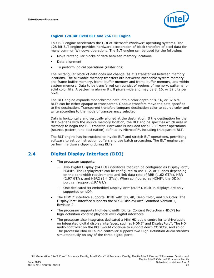
Figure 3. Processor Display Architecture
Me
mo
ry \ C
on
fig
In
terf
ace
Display
Pipe A
Display
Pipe B
Display
Pipe C
Pa
ne
l F
ittin
g
HD Audio
Controller
Transcoder A
DP / HDMI
Timing, VDIP
Transcoder B DP / HDMI
Timing, VDIP
Transcoder C DP / HDMI
Timing, VDIP
eDP* Mux
Transcoder eDP*
DP encoder
Timing, VDIP
DPT, SRID
Po
rt M
ux
Audio
Codec
DP
Aux
eDP
X4 eDP
PC
H D
isp
lay C
on
tro
l S
ign
als
DD
I P
ort
s B
an
d C
X4 DP /
HDMI
X4 DP /
HDMI
Display is the presentation stage of graphics. This involves:
• Pulling rendered data from memory
• Converting raw data into pixels
• Blending surfaces into a frame
• Organizing pixels into frames
• Optionally scaling the image to the desired size
• Re-timing data for the intended target
• Formatting data according to the port output standard
DisplayPort*
DisplayPort* is a digital communication interface that uses differential signaling toachieve a high-bandwidth bus interface designed to support connections between PCsand monitors, projectors, and TV displays.
Processor—Interfaces
5th Generation Intel® Core™ Processor Family, Intel® Core™ M Processor Family, Mobile Intel® Pentium® Processor Family, andMobile Intel® Celeron® Processor FamilyDatasheet – Volume 1 of 2 June 201526 Order No.: 330834-005v1
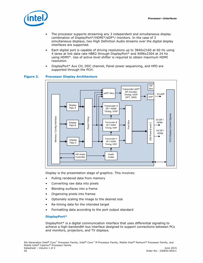
A DisplayPort* consists of a Main Link, Auxiliary channel, and a Hot-Plug Detect signal.The Main Link is a unidirectional, high-bandwidth, and low latency channel used fortransport of isochronous data streams such as uncompressed video and audio. TheAuxiliary Channel (AUX CH) is a half-duplex bidirectional channel used for linkmanagement and device control. The Hot-Plug Detect (HPD) signal serves as aninterrupt request for the sink device.
The processor is designed in accordance with the VESA DisplayPort* Standard Version1.2a. The processor supports VESA DisplayPort* PHY Compliance Test Specification1.2a and VESA DisplayPort* Link Layer Compliance Test Specification 1.2a.
Figure 4. DisplayPort* Overview
Source Device Sink DeviceMain Link(Isochronous Streams)
AUX CH(Link/Device Managemet)
Hot-Plug Detect(Interrupt Request)
DisplayPort Tx DisplayPort Rx
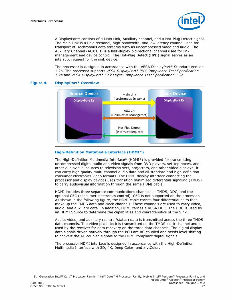
High-Definition Multimedia Interface (HDMI*)
The High-Definition Multimedia Interface* (HDMI*) is provided for transmittinguncompressed digital audio and video signals from DVD players, set-top boxes, andother audiovisual sources to television sets, projectors, and other video displays. Itcan carry high quality multi-channel audio data and all standard and high-definitionconsumer electronics video formats. The HDMI display interface connecting theprocessor and display devices uses transition minimized differential signaling (TMDS)to carry audiovisual information through the same HDMI cable.
HDMI includes three separate communications channels — TMDS, DDC, and theoptional CEC (consumer electronics control). CEC is not supported on the processor.As shown in the following figure, the HDMI cable carries four differential pairs thatmake up the TMDS data and clock channels. These channels are used to carry video,audio, and auxiliary data. In addition, HDMI carries a VESA DDC. The DDC is used byan HDMI Source to determine the capabilities and characteristics of the Sink.
Audio, video, and auxiliary (control/status) data is transmitted across the three TMDSdata channels. The video pixel clock is transmitted on the TMDS clock channel and isused by the receiver for data recovery on the three data channels. The digital displaydata signals driven natively through the PCH are AC coupled and needs level shiftingto convert the AC coupled signals to the HDMI compliant digital signals.
The processor HDMI interface is designed in accordance with the High-DefinitionMultimedia Interface with 3D, 4K, Deep Color, and x.v.Color.
Interfaces—Processor
5th Generation Intel® Core™ Processor Family, Intel® Core™ M Processor Family, Mobile Intel® Pentium® Processor Family, andMobile Intel® Celeron® Processor Family
June 2015 Datasheet – Volume 1 of 2Order No.: 330834-005v1 27
Figure 5. HDMI* Overview
HDMI Source HDMI Sink
TMDS Data Channel 0
Hot-Plug Detect
HDMI Tx HDMI Rx
TMDS Data Channel 1
TMDS Data Channel 2
TMDS Clock Channel
CEC Line (optional)
Display Data Channel (DDC)
embedded DisplayPort*
The embedded DisplayPort* (eDP*) is an embedded version of the DisplayPortstandard oriented towards applications such as notebook and All-In-One PCs. LikeDisplayPort, embedded DisplayPort also consists of a Main Link, Auxiliary channel, andan optional Hot-Plug Detect signal.
Integrated Audio
• HDMI and display port interfaces carry audio along with video.
• Processor supports two DMA controllers to output two High Definition audiostreams on two digital ports simultaneously.
• Supports only the internal HDMI and DP CODECs.
Table 8. Processor Supported Audio Formats over HDMI*and DisplayPort*
Audio Formats HDMI* DisplayPort*
AC-3 Dolby* Digital Yes Yes
Dolby Digital Plus Yes Yes
DTS-HD* Yes Yes
LPCM, 192 kHz/24 bit, 8 Channel Yes Yes
Dolby TrueHD, DTS-HD Master Audio*(Lossless Blu-Ray Disc* Audio Format)
Yes Yes
Processor—Interfaces
5th Generation Intel® Core™ Processor Family, Intel® Core™ M Processor Family, Mobile Intel® Pentium® Processor Family, andMobile Intel® Celeron® Processor FamilyDatasheet – Volume 1 of 2 June 201528 Order No.: 330834-005v1
The processor will continue to support Silent stream. Silent stream is an integratedaudio feature that enables short audio streams, such as system events to be heardover the HDMI and DisplayPort monitors. The processor supports silent streams overthe HDMI and DisplayPort interfaces at 44.1 kHz, 48 kHz, 88.2 kHz, 96 kHz,176.4 kHz, and 192 kHz sampling rates.
Multiple Display Configurations
The following multiple display configuration modes are supported (with appropriatedriver software):
• Single Display is a mode with one display port activated to display the output toone display device. If the external port is activated, it should always use thephysical port B.
• Intel Display Clone is a mode with up to three display ports activated to drive thedisplay content of same color depth setting but potentially different refresh rateand resolution settings to all the active display devices connected.
• Extended Desktop is a mode with up to three display ports activated to drive thecontent with potentially different color depth, refresh rate, and resolution settingson each of the active display devices connected.
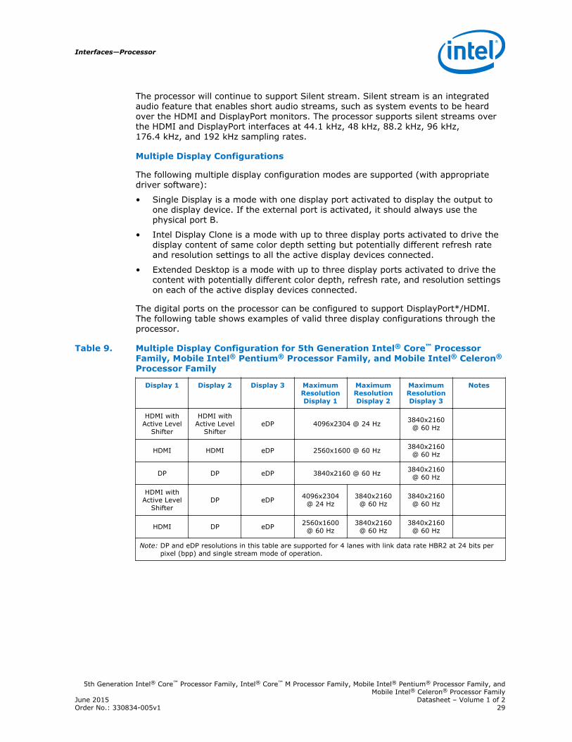
The digital ports on the processor can be configured to support DisplayPort*/HDMI.The following table shows examples of valid three display configurations through theprocessor.
Table 9. Multiple Display Configuration for 5th Generation Intel® Core™ ProcessorFamily, Mobile Intel® Pentium® Processor Family, and Mobile Intel® Celeron®
Processor Family
Display 1 Display 2 Display 3 MaximumResolutionDisplay 1
MaximumResolutionDisplay 2
MaximumResolutionDisplay 3
Notes
HDMI withActive Level
Shifter
HDMI withActive Level
ShiftereDP 4096x2304 @ 24 Hz 3840x2160
@ 60 Hz
HDMI HDMI eDP 2560x1600 @ 60 Hz 3840x2160@ 60 Hz
DP DP eDP 3840x2160 @ 60 Hz 3840x2160@ 60 Hz
HDMI withActive Level
ShifterDP eDP 4096x2304
@ 24 Hz3840x2160
@ 60 Hz3840x2160
@ 60 Hz
HDMI DP eDP 2560x1600@ 60 Hz
3840x2160@ 60 Hz
3840x2160@ 60 Hz
Note: DP and eDP resolutions in this table are supported for 4 lanes with link data rate HBR2 at 24 bits perpixel (bpp) and single stream mode of operation.
Interfaces—Processor
5th Generation Intel® Core™ Processor Family, Intel® Core™ M Processor Family, Mobile Intel® Pentium® Processor Family, andMobile Intel® Celeron® Processor Family
June 2015 Datasheet – Volume 1 of 2Order No.: 330834-005v1 29
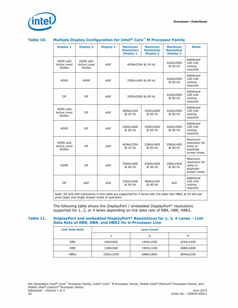
Table 10. Multiple Display Configuration for Intel® Core™ M Processor Family
Display 1 Display 2 Display 3 MaximumResolutionDisplay 1
MaximumResolutionDisplay 2
MaximumResolutionDisplay 3
Notes
HDMI withActive Level
Shifter
HDMI withActive Level
ShiftereDP 4096x2304 @ 24 Hz 3200x2000
@ 60 Hz
Additional100 mWcoolingrequired
HDMI HDMI eDP 2560x1600 @ 60 Hz 3200x2000@ 60 Hz
Additional100 mWcoolingrequired
DP DP eDP 3200x2000 @ 60 Hz 3200x2000@ 60 Hz
Additional100 mWcoolingrequired
HDMI withActive Level
ShifterDP eDP 4096x2304
@ 24 Hz3200x2000
@ 60 Hz3200x2000
@ 60 Hz
Additional100 mWcoolingrequired
HDMI DP eDP 2560x1600@ 60 Hz
3200x2000@ 60 Hz
3200x2000@ 60 Hz
Additional100 mWcoolingrequired
HDMI withActive Level
ShifterDP eDP 4096x2304
@ 24 Hz2560x1600
@ 60 Hz2560x1600
@ 60 Hz
Maximumresolution forclone orduplicatescreen mode.
HDMI DP eDP 2560x1600@ 60 Hz
2560x1600@ 60 Hz
2560x1600@ 60 Hz
Maximumresolution forclone orduplicatescreen mode.
DP eDP N/A 2560x1600@ 60 Hz
3840x2160@ 60 Hz N/A
Additional100 mWcoolingrequired
Note: DP and eDP resolutions in this table are supported for 4 lanes with link data rate HBR2 at 24 bits perpixel (bpp) and single stream mode of operation.
The following table shows the DisplayPort / embedded DisplayPort* resolutionssupported for 1, 2, or 4 lanes depending on link data rate of RBR, HBR, HBR2.
Table 11. DisplayPort and embedded DisplayPort* Resolutions for 1, 2, 4 Lanes – LinkData Rate of RBR, HBR, and HBR2 for U-Processor Line
Link Data Rate Lane Count
1 2 4
RBR 1064x600 1400x1050 2240x1400
HBR 1280x960 1920x1200 2880x1800
HBR2 1920x1200 2880x1800 3840x2160
Processor—Interfaces
5th Generation Intel® Core™ Processor Family, Intel® Core™ M Processor Family, Mobile Intel® Pentium® Processor Family, andMobile Intel® Celeron® Processor FamilyDatasheet – Volume 1 of 2 June 201530 Order No.: 330834-005v1
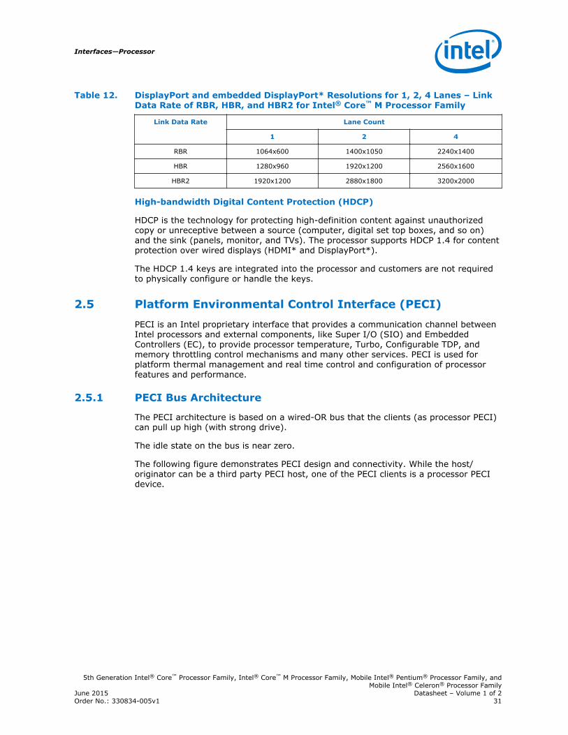
Table 12. DisplayPort and embedded DisplayPort* Resolutions for 1, 2, 4 Lanes – LinkData Rate of RBR, HBR, and HBR2 for Intel® Core™ M Processor Family
Link Data Rate Lane Count
1 2 4
RBR 1064x600 1400x1050 2240x1400
HBR 1280x960 1920x1200 2560x1600
HBR2 1920x1200 2880x1800 3200x2000
High-bandwidth Digital Content Protection (HDCP)
HDCP is the technology for protecting high-definition content against unauthorizedcopy or unreceptive between a source (computer, digital set top boxes, and so on)and the sink (panels, monitor, and TVs). The processor supports HDCP 1.4 for contentprotection over wired displays (HDMI* and DisplayPort*).
The HDCP 1.4 keys are integrated into the processor and customers are not requiredto physically configure or handle the keys.
Platform Environmental Control Interface (PECI)
PECI is an Intel proprietary interface that provides a communication channel betweenIntel processors and external components, like Super I/O (SIO) and EmbeddedControllers (EC), to provide processor temperature, Turbo, Configurable TDP, andmemory throttling control mechanisms and many other services. PECI is used forplatform thermal management and real time control and configuration of processorfeatures and performance.
PECI Bus Architecture
The PECI architecture is based on a wired-OR bus that the clients (as processor PECI)can pull up high (with strong drive).
The idle state on the bus is near zero.
The following figure demonstrates PECI design and connectivity. While the host/originator can be a third party PECI host, one of the PECI clients is a processor PECIdevice.
2.5
2.5.1
Interfaces—Processor
5th Generation Intel® Core™ Processor Family, Intel® Core™ M Processor Family, Mobile Intel® Pentium® Processor Family, andMobile Intel® Celeron® Processor Family
June 2015 Datasheet – Volume 1 of 2Order No.: 330834-005v1 31
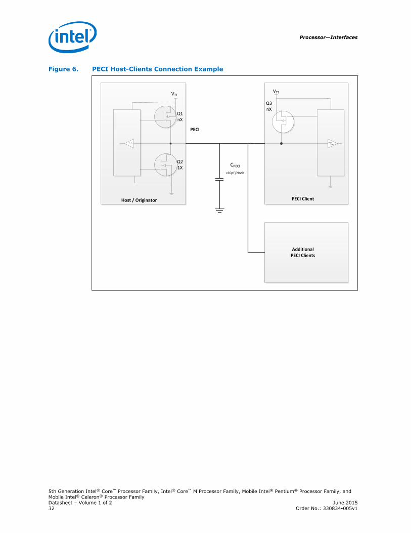
Figure 6. PECI Host-Clients Connection Example
VTT
Host / Originator
Q1nX
Q21X
PECI
CPECI<10pF/Node
Q3nX
VTT
PECI Client
Additional PECI Clients
Processor—Interfaces
5th Generation Intel® Core™ Processor Family, Intel® Core™ M Processor Family, Mobile Intel® Pentium® Processor Family, andMobile Intel® Celeron® Processor FamilyDatasheet – Volume 1 of 2 June 201532 Order No.: 330834-005v1

3.0 Technologies
This chapter provides a high-level description of Intel technologies implemented in theprocessor.
The implementation of the features may vary between the processor SKUs.
Details on the different technologies of Intel processors and other relevant externalnotes are located at the Intel technology web site: http://www.intel.com/technology/
Intel® Virtualization Technology (Intel® VT)
Intel® Virtualization Technology (Intel® VT) makes a single system appear as multipleindependent systems to software. This allows multiple, independent operating systemsto run simultaneously on a single system. Intel VT comprises technology componentsto support virtualization of platforms based on Intel architecture microprocessors andchipsets.
Intel® Virtualization Technology (Intel® VT) for IA-32, Intel® 64 and Intel®Architecture (Intel® VT-x) added hardware support in the processor to improve thevirtualization performance and robustness. Intel® Virtualization Technology forDirected I/O (Intel VT-d) extends Intel® VT-x by adding hardware assisted support toimprove I/O device virtualization performance.
Intel® VT-x specifications and functional descriptions are included in the Intel® 64 andIA-32 Architectures Software Developer’s Manual, Volume 3B and is available at:
http://www.intel.com/products/processor/manuals/index.htm
The Intel VT-d specification and other Intel VT documents can be referenced at:
http://www.intel.com/technology/virtualization/index.htm
https://sharedspaces.intel.com/sites/PCDC/SitePages/Ingredients/ingredient.aspx?ing=VT
Intel® VT-x Objectives
Intel VT-x provides hardware acceleration for virtualization of IA platforms. VirtualMachine Monitor (VMM) can use Intel VT-x features to provide an improved reliablevirtualized platform. By using Intel VT-x, a VMM is:
• Robust: VMMs no longer need to use paravirtualization or binary translation. Thismeans that off-the-shelf operating systems and applications can be run withoutany special steps.
• Enhanced: Intel VT enables VMMs to run 64-bit guest operating systems on IAx86 processors.
3.1
Technologies—Processor
5th Generation Intel® Core™ Processor Family, Intel® Core™ M Processor Family, Mobile Intel® Pentium® Processor Family, andMobile Intel® Celeron® Processor Family
June 2015 Datasheet – Volume 1 of 2Order No.: 330834-005v1 33
• More reliable: Due to the hardware support, VMMs can now be smaller, lesscomplex, and more efficient. This improves reliability and availability and reducesthe potential for software conflicts.
• More secure: The use of hardware transitions in the VMM strengthens theisolation of VMs and further prevents corruption of one VM from affecting otherson the same system.
Intel® VT-x Features
The processor supports the following Intel VT-x features:
• Extended Page Table (EPT) Accessed and Dirty Bits
— EPT A/D bits enabled VMMs to efficiently implement memory management andpage classification algorithms to optimize VM memory operations, such as de-fragmentation, paging, live migration, and check-pointing. Without hardwaresupport for EPT A/D bits, VMMs may need to emulate A/D bits by marking EPTpaging-structures as not-present or read-only, and incur the overhead of EPTpage-fault VM exits and associated software processing.
• Extended Page Table Pointer (EPTP) switching
— EPTP switching is a specific VM function. EPTP switching allows guest software(in VMX non-root operation, supported by EPT) to request a different EPTpaging-structure hierarchy. This is a feature by which software in VMX non-root operation can request a change of EPTP without a VM exit. Software canchoose among a set of potential EPTP values determined in advance bysoftware in VMX root operation.
• Pause loop exiting
— Support VMM schedulers seeking to determine when a virtual processor of amultiprocessor virtual machine is not performing useful work. This situationmay occur when not all virtual processors of the virtual machine are currentlyscheduled and when the virtual processor in question is in a loop involving thePAUSE instruction. The new feature allows detection of such loops and is thuscalled PAUSE-loop exiting.
The processor core supports the following Intel VT-x features:
• Extended Page Tables (EPT)
— EPT is hardware assisted page table virtualization.
— It eliminates VM exits from the guest operating system to the VMM for shadowpage-table maintenance.
• Virtual Processor IDs (VPID)
— Ability to assign a VM ID to tag processor core hardware structures (such asTLBs).
— This avoids flushes on VM transitions to give a lower-cost VM transition timeand an overall reduction in virtualization overhead.
• Guest Preemption Timer
— Mechanism for a VMM to preempt the execution of a guest operating systemafter an amount of time specified by the VMM. The VMM sets a timer valuebefore entering a guest.
— The feature aids VMM developers in flexibility and Quality of Service (QoS)guarantees.
Processor—Technologies
5th Generation Intel® Core™ Processor Family, Intel® Core™ M Processor Family, Mobile Intel® Pentium® Processor Family, andMobile Intel® Celeron® Processor FamilyDatasheet – Volume 1 of 2 June 201534 Order No.: 330834-005v1
• Descriptor-Table Exiting
— Descriptor-table exiting allows a VMM to protect a guest operating systemfrom an internal (malicious software based) attack by preventing relocation ofkey system data structures like IDT (interrupt descriptor table), GDT (globaldescriptor table), LDT (local descriptor table), and TSS (task segmentselector).
— A VMM using this feature can intercept (by a VM exit) attempts to relocatethese data structures and prevent them from being tampered by malicioussoftware.
Intel® VT-d Objectives
The key Intel VT-d objectives are domain-based isolation and hardware-basedvirtualization. A domain can be abstractly defined as an isolated environment in aplatform to which a subset of host physical memory is allocated. Intel VT-d providesaccelerated I/O performance for a virtualized platform and provides software with thefollowing capabilities:
• I/O device assignment and security: for flexibly assigning I/O devices to VMs andextending the protection and isolation properties of VMs for I/O operations.
• DMA remapping: for supporting independent address translations for DirectMemory Accesses (DMA) from devices.
• Interrupt remapping: for supporting isolation and routing of interrupts fromdevices and external interrupt controllers to appropriate VMs.
• Reliability: for recording and reporting to system software DMA and interrupterrors that may otherwise corrupt memory or impact VM isolation.
Intel VT-d accomplishes address translation by associating a transaction from a givenI/O device to a translation table associated with the Guest to which the device isassigned. It does this by means of the data structure in the following illustration. Thistable creates an association between the device's PCI Express* Bus/Device/Function(B/D/F) number and the base address of a translation table. This data structure ispopulated by a VMM to map devices to translation tables in accordance with the deviceassignment restrictions above, and to include a multi-level translation table (VT-dTable) that contains Guest specific address translations.
Technologies—Processor
5th Generation Intel® Core™ Processor Family, Intel® Core™ M Processor Family, Mobile Intel® Pentium® Processor Family, andMobile Intel® Celeron® Processor Family
June 2015 Datasheet – Volume 1 of 2Order No.: 330834-005v1 35
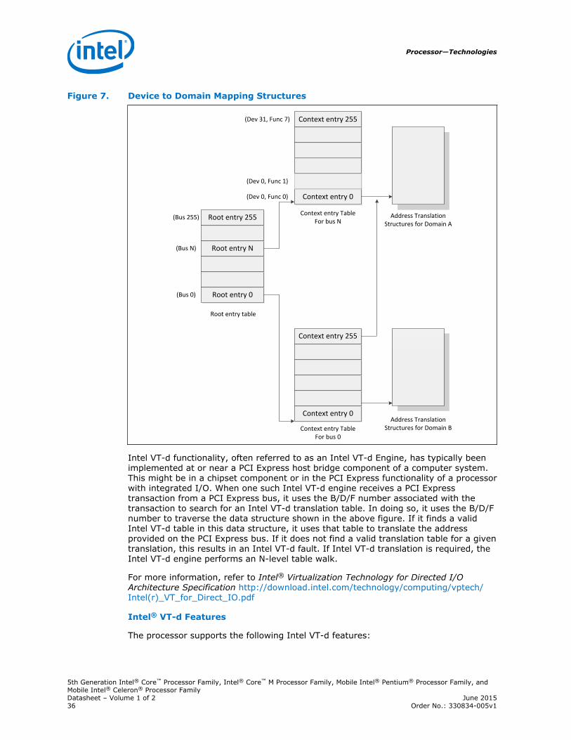
Figure 7. Device to Domain Mapping Structures
Root entry 0
Root entry N
Root entry 255
Context entry 0
Context entry 255
Context entry 0
Context entry 255
(Bus 255)
(Bus N)
(Bus 0)
Root entry table
(Dev 31, Func 7)
(Dev 0, Func 1)
(Dev 0, Func 0)
Context entry TableFor bus N
Context entry TableFor bus 0
Address TranslationStructures for Domain A
Address TranslationStructures for Domain B
Intel VT-d functionality, often referred to as an Intel VT-d Engine, has typically beenimplemented at or near a PCI Express host bridge component of a computer system.This might be in a chipset component or in the PCI Express functionality of a processorwith integrated I/O. When one such Intel VT-d engine receives a PCI Expresstransaction from a PCI Express bus, it uses the B/D/F number associated with thetransaction to search for an Intel VT-d translation table. In doing so, it uses the B/D/Fnumber to traverse the data structure shown in the above figure. If it finds a validIntel VT-d table in this data structure, it uses that table to translate the addressprovided on the PCI Express bus. If it does not find a valid translation table for a giventranslation, this results in an Intel VT-d fault. If Intel VT-d translation is required, theIntel VT-d engine performs an N-level table walk.
For more information, refer to Intel® Virtualization Technology for Directed I/OArchitecture Specification http://download.intel.com/technology/computing/vptech/Intel(r)_VT_for_Direct_IO.pdf
Intel® VT-d Features
The processor supports the following Intel VT-d features:
Processor—Technologies
5th Generation Intel® Core™ Processor Family, Intel® Core™ M Processor Family, Mobile Intel® Pentium® Processor Family, andMobile Intel® Celeron® Processor FamilyDatasheet – Volume 1 of 2 June 201536 Order No.: 330834-005v1

• Memory controller and processor graphics comply with the Intel VT-d 1.2Specification
• Two Intel VT-d DMA remap engines
— iGFX DMA remap engine
— Default DMA remap engine (covers all devices except iGFX)
• Support for root entry, context entry, and default context
• 39-bit guest physical address and host physical address widths
• Support for 4 KB, 2 MB, and 1 GB page sizes
• Support for register-based fault recording only (for single entry only) and supportfor MSI interrupts for faults
• Support for both leaf and non-leaf caching
• Support for boot protection of default page table
• Support for non-caching of invalid page table entries
• Support for hardware-based flushing of translated but pending writes and pendingreads, on IOTLB invalidation
• Support for Global, Domain specific, and Page specific IOTLB invalidation
• MSI cycles (MemWr to address FEEx_xxxxh) not translated
— Translation faults result in cycle forwarding to VBIOS region (byte enablesmasked for writes). Returned data may be bogus for internal agents; PEG/DMIinterfaces return unsupported request status
• Interrupt remapping is supported
• Queued invalidation is supported
• Intel VT-d translation bypass address range is supported (Pass Through)
The processor supports the following added new Intel VT-d features:
• Intel VT-d superpage: support of Intel VT-d superpage (2 MB, 1 GB) for thedefault Intel VT-d engine and Intel VT-D IGD engine (iGFX DMA remap engine
• Support for LPSS device virtualization
Note: Intel VT-d Technology may not be available on all SKUs.
Intel® Trusted Execution Technology (Intel® TXT)
Intel Trusted Execution Technology (Intel TXT) defines platform-level enhancementsthat provide the building blocks for creating trusted platforms.
The Intel TXT platform helps to provide the authenticity of the controlling environmentsuch that those wishing to rely on the platform can make an appropriate trustdecision. The Intel TXT platform determines the identity of the controlling environmentby accurately measuring and verifying the controlling software.
Another aspect of the trust decision is the ability of the platform to resist attempts tochange the controlling environment. The Intel TXT platform will resist attempts bysoftware processes to change the controlling environment or bypass the bounds set bythe controlling environment.
3.2
Technologies—Processor
5th Generation Intel® Core™ Processor Family, Intel® Core™ M Processor Family, Mobile Intel® Pentium® Processor Family, andMobile Intel® Celeron® Processor Family
June 2015 Datasheet – Volume 1 of 2Order No.: 330834-005v1 37
Intel TXT is a set of extensions designed to provide a measured and controlled launchof system software that will then establish a protected environment for itself and anyadditional software that it may execute.
These extensions enhance two areas:
• The launching of the Measured Launched Environment (MLE).
• The protection of the MLE from potential corruption.
The enhanced platform provides these launch and control interfaces using Safer ModeExtensions (SMX).
The SMX interface includes the following functions:
• Measured/Verified launch of the MLE.
• Mechanisms to ensure the above measurement is protected and stored in a securelocation.
• Protection mechanisms that allow the MLE to control attempts to modify itself.
The processor also offers additional enhancements to System Management Mode(SMM) architecture for enhanced security and performance. The processor providesnew MSRs to:
• Enable a second SMM range
• Enable SMM code execution range checking
• Select whether SMM Save State is to be written to legacy SMRAM or to MSRs
• Determine if a thread is going to be delayed entering SMM
• Determine if a thread is blocked from entering SMM
• Targeted SMI, enable/disable threads from responding to SMIs both VLWs and IPI
For the above features, BIOS must test the associated capability bit before attemptingto access any of the above registers.
For more information, refer to the Intel® Trusted Execution Technology MeasuredLaunched Environment Programming Guide.
Intel® Hyper-Threading Technology (Intel® HTTechnology)
The processor supports Intel Hyper-Threading Technology (Intel HT Technology) thatallows an execution core to function as two logical processors. While some executionresources, such as caches, execution units, and buses are shared, each logicalprocessor has its own architectural state with its own set of general-purpose registersand control registers. This feature must be enabled using the BIOS and requiresoperating system support.
Intel recommends enabling Intel HT Technology with Microsoft Windows* 8 ,Windows* 8.1, and Microsoft Windows* 7 and disabling Intel HT Technology using theBIOS for all previous versions of Windows* operating systems. For more informationon Intel HT Technology, see http://www.intel.com/technology/platform-technology/hyper-threading/.
3.3
Processor—Technologies
5th Generation Intel® Core™ Processor Family, Intel® Core™ M Processor Family, Mobile Intel® Pentium® Processor Family, andMobile Intel® Celeron® Processor FamilyDatasheet – Volume 1 of 2 June 201538 Order No.: 330834-005v1
Intel® Turbo Boost Technology 2.0
The Intel Turbo Boost Technology 2.0 allows the processor core to opportunisticallyand automatically run faster than its rated operating frequency/render clock, if it isoperating below power, temperature, and current limits. The Intel Turbo BoostTechnology 2.0 feature is designed to increase performance of both multi-threadedand single-threaded workloads.
Compared with previous generation products, Intel Turbo Boost Technology 2.0 willincrease the ratio of application power to TDP. Thus, thermal solutions and platformcooling that are designed to less than thermal design guidance might experiencethermal and performance issues since more applications will tend to run at themaximum power limit for significant periods of time.
Note: Intel Turbo Boost Technology 2.0 may not be available on all SKUs.
Intel® Turbo Boost Technology 2.0 Frequency
To determine the highest performance frequency amongst active cores, the processortakes the following into consideration:
• The number of cores operating in the C0 state.
• The estimated core current consumption.
• The estimated package prior and present power consumption.
• The package temperature.
Any of these factors can affect the maximum frequency for a given workload. If thepower, current, or thermal limit is reached, the processor will automatically reduce thefrequency to stay within its TDP limit. Turbo processor frequencies are only active ifthe operating system is requesting the P0 state. For more information on P-states andC-states, see Power Management on page 44.
Intel® Advanced Vector Extensions 2.0 (Intel® AVX2)
Intel Advanced Vector Extensions 2.0 (Intel AVX2) is the latest expansion of the Intelinstruction set. Intel AVX2 extends the Intel Advanced Vector Extensions (Intel AVX)with 256-bit integer instructions, floating-point fused multiply add (FMA) instructions,and gather operations. The 256-bit integer vectors benefit math, codec, image, anddigital signal processing software. FMA improves performance in face detection,professional imaging, and high performance computing. Gather operations increasevectorization opportunities for many applications. In addition to the vector extensions,this generation of Intel processors adds new bit manipulation instructions useful incompression, encryption, and general purpose software.
For more information on Intel AVX, see http://www.intel.com/software/avx
Intel® Advanced Encryption Standard New Instructions(Intel® AES-NI)
The processor supports Intel Advanced Encryption Standard New Instructions (IntelAES-NI) that are a set of Single Instruction Multiple Data (SIMD) instructions thatenable fast and secure data encryption and decryption based on the AdvancedEncryption Standard (AES). Intel AES-NI are valuable for a wide range of
3.4
3.5
3.6
Technologies—Processor
5th Generation Intel® Core™ Processor Family, Intel® Core™ M Processor Family, Mobile Intel® Pentium® Processor Family, andMobile Intel® Celeron® Processor Family
June 2015 Datasheet – Volume 1 of 2Order No.: 330834-005v1 39
cryptographic applications, such as applications that perform bulk encryption/decryption, authentication, random number generation, and authenticated encryption.AES is broadly accepted as the standard for both government and industryapplications, and is widely deployed in various protocols.
Intel AES-NI consists of six Intel SSE instructions. Four instructions, AESENC,AESENCLAST, AESDEC, and AESDELAST facilitate high performance AES encryptionand decryption. The other two, AESIMC and AESKEYGENASSIST, support the AES keyexpansion procedure. Together, these instructions provide a full hardware forsupporting AES; offering security, high performance, and a great deal of flexibility.
PCLMULQDQ Instruction
The processor supports the carry-less multiplication instruction, PCLMULQDQ.PCLMULQDQ is a Single Instruction Multiple Data (SIMD) instruction that computes the128-bit carry-less multiplication of two, 64-bit operands without generating andpropagating carries. Carry-less multiplication is an essential processing component ofseveral cryptographic systems and standards. Hence, accelerating carry-lessmultiplication can significantly contribute to achieving high speed secure computingand communication.
Intel® Secure Key
The processor supports Intel® Secure Key (formerly known as Digital Random NumberGenerator (DRNG)), a software visible random number generation mechanismsupported by a high quality entropy source. This capability is available toprogrammers through the RDRAND instruction. The resultant random numbergeneration capability is designed to comply with existing industry standards in thisregard (ANSI X9.82 and NIST SP 800-90).
Some possible usages of the RDRAND instruction include cryptographic key generationas used in a variety of applications, including communication, digital signatures,secure storage, and so on.
The processor has a RDSEED instruction that enables system software and securityvendors who need to seed or reseed a software PRNG.
The RDSEED instruction will be a companion to the RDRAND instruction. RDSEED,along with RDRAND, fills out Intel's standards compliant (such as NIST SP800-90 A, B,and C) Hardware-based Random Number Generator portfolio.
Intel® 64 Architecture x2APIC
The x2APIC architecture extends the xAPIC architecture that provides keymechanisms for interrupt delivery. This extension is primarily intended to increaseprocessor addressability.
Specifically, x2APIC:
• Retains all key elements of compatibility to the xAPIC architecture:
— Delivery modes
— Interrupt and processor priorities
— Interrupt sources
— Interrupt destination types
3.7
Processor—Technologies
5th Generation Intel® Core™ Processor Family, Intel® Core™ M Processor Family, Mobile Intel® Pentium® Processor Family, andMobile Intel® Celeron® Processor FamilyDatasheet – Volume 1 of 2 June 201540 Order No.: 330834-005v1

• Provides extensions to scale processor addressability for both the logical andphysical destination modes
• Adds new features to enhance performance of interrupt delivery
• Reduces complexity of logical destination mode interrupt delivery on link basedarchitectures
The key enhancements provided by the x2APIC architecture over xAPIC are thefollowing:
• Support for two modes of operation to provide backward compatibility andextensibility for future platform innovations:
— In xAPIC compatibility mode, APIC registers are accessed through memorymapped interface to a 4K-Byte page, identical to the xAPIC architecture.
— In x2APIC mode, APIC registers are accessed through Model Specific Register(MSR) interfaces. In this mode, the x2APIC architecture provides significantlyincreased processor addressability and some enhancements on interruptdelivery.
• Increased range of processor addressability in x2APIC mode:
— Physical xAPIC ID field increases from 8 bits to 32 bits, allowing for interruptprocessor addressability up to 4G–1 processors in physical destination mode.A processor implementation of x2APIC architecture can support fewer than 32-bits in a software transparent fashion.
— Logical xAPIC ID field increases from 8 bits to 32 bits. The 32-bit logicalx2APIC ID is partitioned into two sub-fields – a 16-bit cluster ID and a 16-bitlogical ID within the cluster. Consequently, ((2^20) – 16) processors can beaddressed in logical destination mode. Processor implementations can supportfewer than 16 bits in the cluster ID sub-field and logical ID sub-field in asoftware agnostic fashion.
• More efficient MSR interface to access APIC registers:
— To enhance inter-processor and self-directed interrupt delivery as well as theability to virtualize the local APIC, the APIC register set can be accessed onlythrough MSR-based interfaces in x2APIC mode. The Memory Mapped IO(MMIO) interface used by xAPIC is not supported in x2APIC mode.
• The semantics for accessing APIC registers have been revised to simplify theprogramming of frequently-used APIC registers by system software. Specifically,the software semantics for using the Interrupt Command Register (ICR) and EndOf Interrupt (EOI) registers have been modified to allow for more efficient deliveryand dispatching of interrupts.
• The x2APIC extensions are made available to system software by enabling thelocal x2APIC unit in the “x2APIC” mode. To benefit from x2APIC capabilities, anew operating system and a new BIOS are both needed, with special support forx2APIC mode.
• The x2APIC architecture provides backward compatibility to the xAPIC architectureand forward extendible for future Intel platform innovations.
Note: Intel x2APIC Technology may not be available on all SKUs.
For more information, see the Intel® 64 Architecture x2APIC Specification at http://www.intel.com/products/processor/manuals/.
Technologies—Processor
5th Generation Intel® Core™ Processor Family, Intel® Core™ M Processor Family, Mobile Intel® Pentium® Processor Family, andMobile Intel® Celeron® Processor Family
June 2015 Datasheet – Volume 1 of 2Order No.: 330834-005v1 41
Power Aware Interrupt Routing (PAIR)
The processor includes enhanced power-performance technology that routesinterrupts to threads or cores based on their sleep states. As an example, for energysavings, it routes the interrupt to the active cores without waking the deep idle cores.For performance, it routes the interrupt to the idle (C1) cores without interrupting thealready heavily loaded cores. This enhancement is mostly beneficial for high-interruptscenarios like Gigabit LAN, WLAN peripherals, and so on.
Execute Disable Bit
The Execute Disable Bit allows memory to be marked as executable when combinedwith a supporting operating system. If code attempts to run in non-executablememory, the processor raises an error to the operating system. This feature canprevent some classes of viruses or worms that exploit buffer overrun vulnerabilitiesand can thus help improve the overall security of the system. See the Intel® 64 andIA-32 Architectures Software Developer's Manuals for more detailed information.
Intel® Device Protection with Boot Guard
Intel® Device Protection with Boot Guard can help protect the platform boot integrityby preventing execution of unauthorized boot blocks. With Intel® Device Protectionwith Boot Guard, platform manufacturers can create boot policies such that invocationof an unauthorized (or untrusted) boot block will trigger the platform protection perthe manufacturer's defined policy.
With verification based in the hardware, Intel® Device Protection with Boot Guardextends the trust boundary of the platform boot process down to the hardware level.
Intel® Device Protection with Boot Guard accomplishes this by:
• Providing hardware-based Static Root of Trust for Measurement (S-RTM) and theRoot of Trust for Verification (RTV) using Intel architectural components.
• Providing architectural definition for platform manufacturer Boot Policy.
• Enforcing manufacture provided Boot Policy using Intel architectural components.
Benefits of this protection is that Intel® Device Protection with Boot Guard can helpmaintain platform integrity by preventing re-purposing of the manufacturer’shardware to run an unauthorized software stack.
Note: Intel® Device Protection with Boot Guard technology availability may vary betweenthe different SKUs.
Supervisor Mode Execution Protection (SMEP)
Supervisor Mode Execution Protection provides the next level of system protection byblocking malicious software attacks from user mode code when the system is runningin the highest privilege level. This technology helps to protect from virus attacks andunwanted code from harming the system. For more information, refer to Intel® 64and IA-32 Architectures Software Developer's Manual, Volume 3A at: http://www.intel.com/Assets/PDF/manual/253668.pdf
3.8
3.9
3.10
3.11
Processor—Technologies
5th Generation Intel® Core™ Processor Family, Intel® Core™ M Processor Family, Mobile Intel® Pentium® Processor Family, andMobile Intel® Celeron® Processor FamilyDatasheet – Volume 1 of 2 June 201542 Order No.: 330834-005v1
Supervisor Mode Access Protection (SMAP)
Supervisor Mode Access Protection provides the next level of system protection byblocking a malicious user from tricking the operating system into branching off userdata. This technology shuts down very popular attack vectors against operatingsystems . For more information, refer to the Intel® 64 and IA-32 ArchitecturesSoftware Developer's Manual, Volume 3A.
Intel® Transactional Synchronization Extensions - NewInstructions (Intel® TSX-NI)
The processor supports Intel Transactional Synchronization Extensions - NewInstructions (Intel TSX-NI). Intel TSX-NI provides a set of instruction extensions thatallow programmers to specify regions of code for transactional synchronization.Programmers can use these extensions to achieve the performance of fine-grainlocking while actually programming using coarse-grain locks. Details on Intel TSX-NIare in the Intel® Architecture Instruction Set Extensions Programming Reference.
3.12
3.13
Technologies—Processor
5th Generation Intel® Core™ Processor Family, Intel® Core™ M Processor Family, Mobile Intel® Pentium® Processor Family, andMobile Intel® Celeron® Processor Family
June 2015 Datasheet – Volume 1 of 2Order No.: 330834-005v1 43
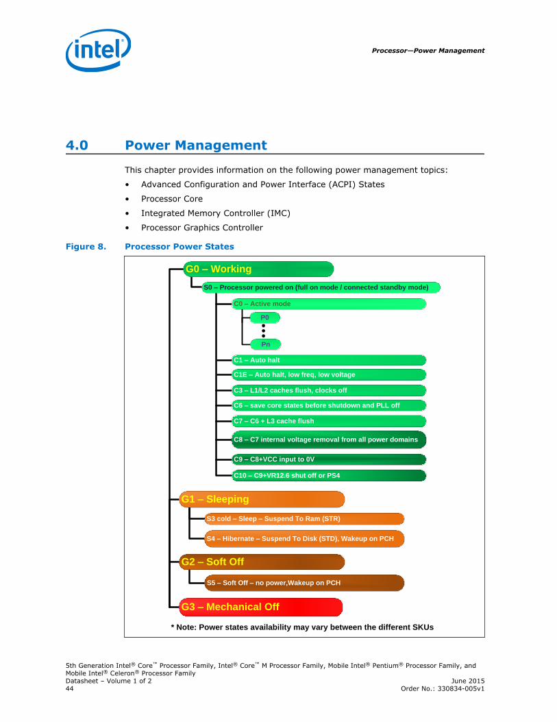
4.0 Power Management
This chapter provides information on the following power management topics:
• Advanced Configuration and Power Interface (ACPI) States
• Processor Core
• Integrated Memory Controller (IMC)
• Processor Graphics Controller
Figure 8. Processor Power States
G0 – Working
S0 – Processor powered on (full on mode / connected standby mode)
C0 – Active mode
C1 – Auto halt
C1E – Auto halt, low freq, low voltage
C3 – L1/L2 caches flush, clocks off
C6 – save core states before shutdown and PLL off
C7 – C6 + L3 cache flush
G1 – Sleeping
S3 cold – Sleep – Suspend To Ram (STR)
S4 – Hibernate – Suspend To Disk (STD), Wakeup on PCH
S5 – Soft Off – no power,Wakeup on PCH
G3 – Mechanical Off
P0
Pn
* Note: Power states availability may vary between the different SKUs
C8 – C7 internal voltage removal from all power domains
C9 – C8+VCC input to 0V
C10 – C9+VR12.6 shut off or PS4
G2 – Soft Off
Processor—Power Management
5th Generation Intel® Core™ Processor Family, Intel® Core™ M Processor Family, Mobile Intel® Pentium® Processor Family, andMobile Intel® Celeron® Processor FamilyDatasheet – Volume 1 of 2 June 201544 Order No.: 330834-005v1
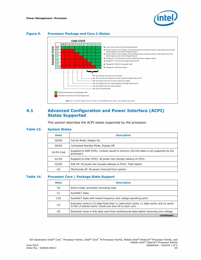
Figure 9. Processor Package and Core C-States
One or more cores or GT executing instructions
All cores and GT in C3 or deeper, L3 may be flushed and turned off, memory in self refresh, some Uncore clocks stopped, some Uncore voltages reduced
All cores and GT in C6 or deeper, L3 may be flushed and turned off, memory in self refresh, all Uncore clocks stopped, some Uncore voltages reduced
Package C6 + L3 flushed and turned off, additional Uncore voltages reduced
Package C7 + most Uncore voltages reduced to 0V
Package C8 + VR12.6 in low power state
Package C9 + VR12.6 turned off
All core clocks are stopped, core state saved and voltage reduce to 0V
Cores flush L1/L2 into L3, all core clocks are stopped
Core halted, most core clocks stopped and voltage reduced to Pn
Core halted, most core clocks stopped
Core is executing code
C0 C1 C1E C3 C6 C7 C8 C9 C10C0C3C6C7C8C9C10
PA
CK
AG
E ST
ATE
CORE STATE
Core behaves the same as Core C6 state
Possible combination of core/package states
Impossible combination of core/package states
Note: The “core state” relates to the core which is in the HIGHEST power state in the package (most active)
{
Advanced Configuration and Power Interface (ACPI)States Supported
This section describes the ACPI states supported by the processor.
Table 13. System States
State Description
G0/S0 Full On Mode, Display On.
G0/S0 Connected Standby Mode, Display Off.
G1/S3-Cold Suspend-to-RAM (STR). Context saved to memory (S3-Hot state is not supported by theprocessor).
G1/S4 Suspend-to-Disk (STD). All power lost (except wakeup on PCH).
G2/S5 Soft off. All power lost (except wakeup on PCH). Total reboot.
G3 Mechanical off. All power removed from system.
Table 14. Processor Core / Package State Support
State Description
C0 Active mode, processor executing code.
C1 AutoHALT state.
C1E AutoHALT state with lowest frequency and voltage operating point.
C3 Execution cores in C3 state flush their L1 instruction cache, L1 data cache, and L2 cacheto the L3 shared cache. Clocks are shut off to each core.
C6 Execution cores in this state save their architectural state before removing core voltage.
continued...
4.1
Power Management—Processor
5th Generation Intel® Core™ Processor Family, Intel® Core™ M Processor Family, Mobile Intel® Pentium® Processor Family, andMobile Intel® Celeron® Processor Family
June 2015 Datasheet – Volume 1 of 2Order No.: 330834-005v1 45
State Description
C7
Execution cores in this state behave similarly to the C6 state. If all execution coresrequest C7 state, L3 cache ways are flushed until it is cleared. If the entire L3 cache isflushed, voltage will be removed from the L3 cache. Power removal to SA, Cores and L3will reduce power consumption.
C8 C7 state plus voltage is removed from all power domains after required state is saved. PLLis powered down.
C9 C8 state plus processor VCC input voltage at 0 V.
C10 C9 state plus VR12.6 is set to low-power state, near shut off.
Table 15. Integrated Memory Controller States
State Description
Power up CKE asserted. Active mode.
Pre-chargePower-down
CKE de-asserted (not self-refresh) with all banks closed.
Active Power-down
CKE de-asserted (not self-refresh) with minimum one bank active.
Self-Refresh CKE de-asserted using device self-refresh.
Table 16. G, S, and C Interface State Combinations
Global(G)
State
Sleep (S)State
ProcessorPackage (C)
State
ProcessorState
System Clocks Description
G0 S0 C0 Full On On Full On
G0 S0 C1/C1E Auto-Halt On Auto-Halt
G0 S0 C3 Deep Sleep On Deep Sleep
G0 S0 C6/C7 Deep Power-down On Deep Power-down
G0 S0 C8/C9/C10 On Deeper Power-down
G1 S3 Power off Off, except RTC Suspend to RAM
G1 S4 Power off Off, except RTC Suspend to Disk
G2 S5 Power off Off, except RTC Soft Off
G3 NA Power off Power off Hard off
Processor Core Power Management
While executing code, Enhanced Intel SpeedStep® Technology optimizes theprocessor’s frequency and core voltage based on workload. Each frequency andvoltage operating point is defined by ACPI as a P-state. When the processor is notexecuting code, it is idle. A low-power idle state is defined by ACPI as a C-state. Ingeneral, deeper power C-states have longer entry and exit latencies.
Enhanced Intel SpeedStep® Technology Key Features
The following are the key features of Enhanced Intel SpeedStep Technology:
4.2
4.2.1
Processor—Power Management
5th Generation Intel® Core™ Processor Family, Intel® Core™ M Processor Family, Mobile Intel® Pentium® Processor Family, andMobile Intel® Celeron® Processor FamilyDatasheet – Volume 1 of 2 June 201546 Order No.: 330834-005v1

• Multiple frequency and voltage points for optimal performance and powerefficiency. These operating points are known as P-states.
• Frequency selection is software controlled by writing to processor MSRs. Thevoltage is optimized based on the selected frequency and the number of activeprocessor cores.
— Once the voltage is established, the PLL locks on to the target frequency.
— All active processor cores share the same frequency and voltage. In a multi-core processor, the highest frequency P-state requested among all activecores is selected.
— Software-requested transitions are accepted at any time. If a previoustransition is in progress, the new transition is deferred until the previoustransition is completed.
• The processor controls voltage ramp rates internally to ensure glitch-freetransitions.
• Because there is low transition latency between P-states, a significant number oftransitions per-second are possible.
Low-Power Idle States
When the processor is idle, low-power idle states (C-states) are used to save power.More power savings actions are taken for numerically higher C-states. However,higher C-states have longer exit and entry latencies. Resolution of C-states occur atthe thread, processor core, and processor package level. Thread-level C-states areavailable if Intel Hyper-Threading Technology is enabled.
Caution: Long term reliability cannot be assured unless all the Low-Power Idle States areenabled.
Figure 10. Idle Power Management Breakdown of the Processor Cores
Thread 0 Thread 1
Core 0 State
Thread 0 Thread 1
Core N State
Processor Package State
4.2.2
Power Management—Processor
5th Generation Intel® Core™ Processor Family, Intel® Core™ M Processor Family, Mobile Intel® Pentium® Processor Family, andMobile Intel® Celeron® Processor Family
June 2015 Datasheet – Volume 1 of 2Order No.: 330834-005v1 47
While individual threads can request low-power C-states, power saving actions onlytake place once the core C-state is resolved. Core C-states are automatically resolvedby the processor. For thread and core C-states, a transition to and from C0 is requiredbefore entering any other C-state.
Requesting Low-Power Idle States
The primary software interfaces for requesting low-power idle states are through theMWAIT instruction with sub-state hints and the HLT instruction (for C1 and C1E).However, software may make C-state requests using the legacy method of I/O readsfrom the ACPI-defined processor clock control registers, referred to as P_LVLx. Thismethod of requesting C-states provides legacy support for operating systems thatinitiate C-state transitions using I/O reads.
For legacy operating systems, P_LVLx I/O reads are converted within the processor tothe equivalent MWAIT C-state request. Therefore, P_LVLx reads do not directly resultin I/O reads to the system. The feature, known as I/O MWAIT redirection, must beenabled in the BIOS.
The BIOS can write to the C-state range field of the PMG_IO_CAPTURE MSR to restrictthe range of I/O addresses that are trapped and emulate MWAIT like functionality.Any P_LVLx reads outside of this range do not cause an I/O redirection to MWAIT(Cx)like request. The reads fall through like a normal I/O instruction.
Note: When P_LVLx I/O instructions are used, MWAIT sub-states cannot be defined. TheMWAIT sub-state is always zero if I/O MWAIT redirection is used. By default, P_LVLxI/O redirections enable the MWAIT 'break on EFLAGS.IF’ feature that triggers awakeup on an interrupt, even if interrupts are masked by EFLAGS.IF.
Core C-State Rules
The following are general rules for all core C-states, unless specified otherwise:
• A core C-state is determined by the lowest numerical thread state (such as Thread0 requests C1E state while Thread 1 requests C3 state, resulting in a core C1Estate). See the G, S, and C Interface State Combinations table.
• A core transitions to C0 state when:
— An interrupt occurs
— There is an access to the monitored address if the state was entered using anMWAIT/Timed MWAIT instruction
— The deadline corresponding to the Timed MWAIT instruction expires
• An interrupt directed toward a single thread wakes only that thread.
• If any thread in a core is in active (in C0 state), the core's C-state will resolve toC0 state.
• Any interrupt coming into the processor package may wake any core.
• A system reset re-initializes all processor cores.
Core C0 State
The normal operating state of a core where code is being executed.
4.2.3
4.2.4
Processor—Power Management
5th Generation Intel® Core™ Processor Family, Intel® Core™ M Processor Family, Mobile Intel® Pentium® Processor Family, andMobile Intel® Celeron® Processor FamilyDatasheet – Volume 1 of 2 June 201548 Order No.: 330834-005v1
Core C1/C1E State
C1/C1E is a low power state entered when all threads within a core execute a HLT orMWAIT(C1/C1E) instruction.
A System Management Interrupt (SMI) handler returns execution to either Normalstate or the C1/C1E state. See the Intel® 64 and IA-32 Architectures SoftwareDeveloper’s Manual for more information.
While a core is in C1/C1E state, it processes bus snoops and snoops from otherthreads. For more information on C1E state, see Package C-States on page 50.
Core C3 State
Individual threads of a core can enter the C3 state by initiating a P_LVL2 I/O read tothe P_BLK or an MWAIT(C3) instruction. A core in C3 state flushes the contents of itsL1 instruction cache, L1 data cache, and L2 cache to the shared L3 cache, whilemaintaining its architectural state. All core clocks are stopped at this point. Becausethe core’s caches are flushed, the processor does not wake any core that is in the C3state when either a snoop is detected or when another core accesses cacheablememory.
Core C6 State
Individual threads of a core can enter the C6 state by initiating a P_LVL3 I/O read oran MWAIT(C6) instruction. Before entering core C6 state, the core will save itsarchitectural state to a dedicated SRAM. Once complete, a core will have its voltagereduced to zero volts. During exit, the core is powered on and its architectural state isrestored.
Core C7-C10 States
Individual threads of a core can enter the C7, C8, C9, or C10 state by initiating aP_LVL4, P_LVL5, P_LVL6, P_LVL7 I/O read (respectively) to the P_BLK or by anMWAIT(C7/C8/C9/C10) instruction. The core C7–C10 state exhibits the same behavioras the core C6 state.
C-State Auto-Demotion
In general, deeper C-states, such as C6 or C7 state, have long latencies and havehigher energy entry/exit costs. The resulting performance and energy penaltiesbecome significant when the entry/exit frequency of a deeper C-state is high.Therefore, incorrect or inefficient usage of deeper C-states have a negative impact onbattery life and idle power. To increase residency and improve battery life and idlepower in deeper C-states, the processor supports C-state auto-demotion.
There are two C-state auto-demotion options:
• C7/C6 to C3 state
• C7/C6/C3 To C1 state
The decision to demote a core from C6/C7 to C3 or C3/C6/C7 to C1 state is based oneach core’s immediate residency history and interrupt rate . If the interrupt rateexperienced on a core is high and the residence in a deep C-state between suchinterrupts is low, the core can be demoted to a C3 or C1 state. A higher interruptpattern is required to demote a core to C1 state as compared to C3 state.
Power Management—Processor
5th Generation Intel® Core™ Processor Family, Intel® Core™ M Processor Family, Mobile Intel® Pentium® Processor Family, andMobile Intel® Celeron® Processor Family
June 2015 Datasheet – Volume 1 of 2Order No.: 330834-005v1 49
This feature is disabled by default. BIOS must enable it in thePMG_CST_CONFIG_CONTROL register. The auto-demotion policy is also configured bythis register.
Package C-States
The processor supports C0, C1/C1E, C3, C6, C7, C8, C9, and C10 power states.Thefollowing is a summary of the general rules for package C-state entry. These apply toall package C-states, unless specified otherwise:
• A package C-state request is determined by the lowest numerical core C-stateamongst all cores.
• A package C-state is automatically resolved by the processor depending on thecore idle power states and the status of the platform components.
— Each core can be at a lower idle power state than the package if the platformdoes not grant the processor permission to enter a requested package C-state.
— The platform may allow additional power savings to be realized in theprocessor.
— For package C-states, the processor is not required to enter C0 state beforeentering any other C-state.
— Entry into a package C-state may be subject to auto-demotion – that is, theprocessor may keep the package in a deeper package C-state than requestedby the operating system if the processor determines, using heuristics, that thedeeper C-state results in better power/performance.
The processor exits a package C-state when a break event is detected. Depending onthe type of break event, the processor does the following:
• If a core break event is received, the target core is activated and the break eventmessage is forwarded to the target core.
— If the break event is not masked, the target core enters the core C0 state andthe processor enters package C0 state.
— If the break event is masked, the processor attempts to re-enter its previouspackage state.
• If the break event was due to a memory access or snoop request,
— But the platform did not request to keep the processor in a higher package C-state, the package returns to its previous C-state.
— And the platform requests a higher power C-state, the memory access orsnoop request is serviced and the package remains in the higher power C-state.
The following table shows package C-state resolution for a dual-core processor. Thefollowing figure summarizes package C-state transitions.
4.2.5
Processor—Power Management
5th Generation Intel® Core™ Processor Family, Intel® Core™ M Processor Family, Mobile Intel® Pentium® Processor Family, andMobile Intel® Celeron® Processor FamilyDatasheet – Volume 1 of 2 June 201550 Order No.: 330834-005v1
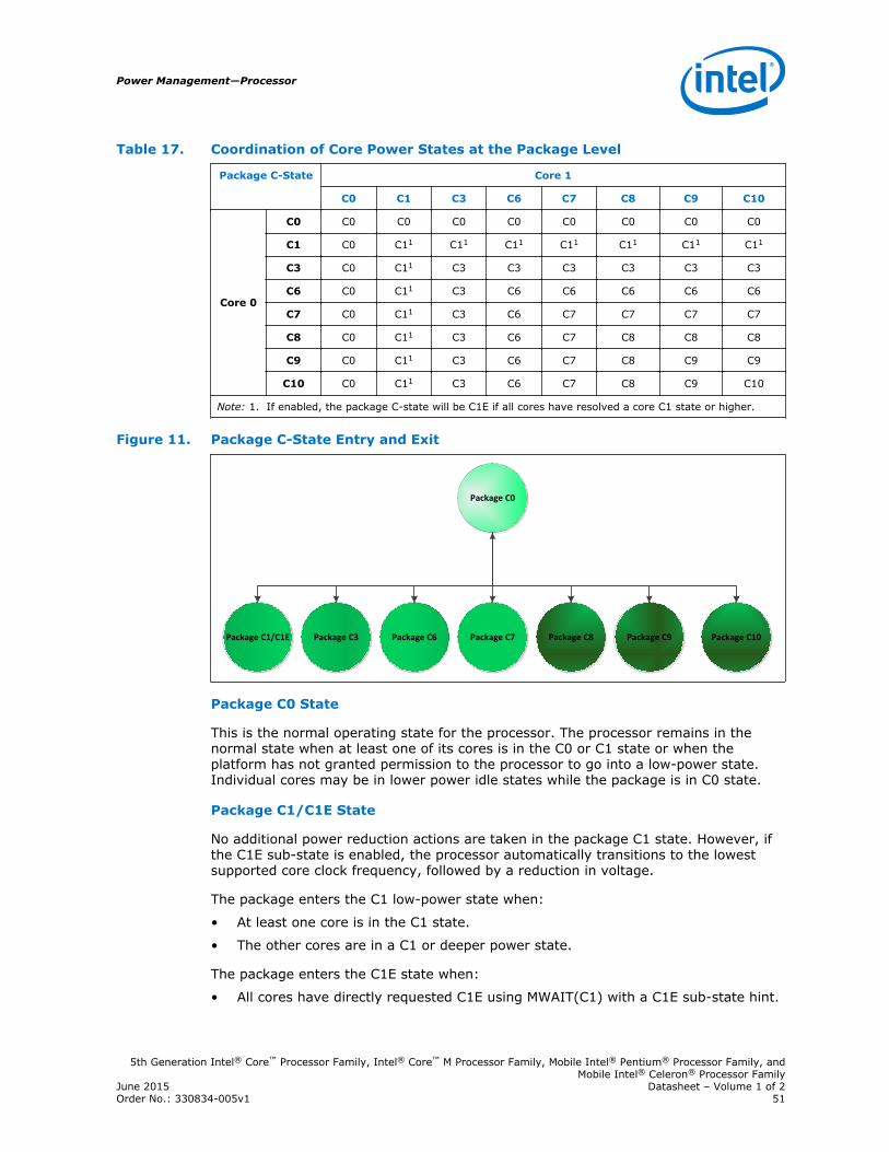
Table 17. Coordination of Core Power States at the Package Level
Package C-State Core 1
C0 C1 C3 C6 C7 C8 C9 C10
Core 0
C0 C0 C0 C0 C0 C0 C0 C0 C0
C1 C0 C11 C11 C11 C11 C11 C11 C11
C3 C0 C11 C3 C3 C3 C3 C3 C3
C6 C0 C11 C3 C6 C6 C6 C6 C6
C7 C0 C11 C3 C6 C7 C7 C7 C7
C8 C0 C11 C3 C6 C7 C8 C8 C8
C9 C0 C11 C3 C6 C7 C8 C9 C9
C10 C0 C11 C3 C6 C7 C8 C9 C10
Note: 1. If enabled, the package C-state will be C1E if all cores have resolved a core C1 state or higher.
Figure 11. Package C-State Entry and Exit
Package C0
Package C7 Package C6Package C3 Package C9Package C8 Package C10Package C1/C1E
Package C0 State
This is the normal operating state for the processor. The processor remains in thenormal state when at least one of its cores is in the C0 or C1 state or when theplatform has not granted permission to the processor to go into a low-power state.Individual cores may be in lower power idle states while the package is in C0 state.
Package C1/C1E State
No additional power reduction actions are taken in the package C1 state. However, ifthe C1E sub-state is enabled, the processor automatically transitions to the lowestsupported core clock frequency, followed by a reduction in voltage.
The package enters the C1 low-power state when:
• At least one core is in the C1 state.
• The other cores are in a C1 or deeper power state.
The package enters the C1E state when:
• All cores have directly requested C1E using MWAIT(C1) with a C1E sub-state hint.
Power Management—Processor
5th Generation Intel® Core™ Processor Family, Intel® Core™ M Processor Family, Mobile Intel® Pentium® Processor Family, andMobile Intel® Celeron® Processor Family
June 2015 Datasheet – Volume 1 of 2Order No.: 330834-005v1 51
• All cores are in a power state deeper than C1/C1E state; however, the packagelow-power state is limited to C1/C1E using the PMG_CST_CONFIG_CONTROL MSR.
• All cores have requested C1 state using HLT or MWAIT(C1) and C1E auto-promotion is enabled in IA32_MISC_ENABLES.
No notification to the system occurs upon entry to C1/C1E state.
Package C2 State
Package C2 state is an internal processor state that cannot be explicitly requested bysoftware. A processor enters Package C2 state when:
• All cores and graphics have requested a C3 or deeper power state; however,constraints (LTR, programmed timer events in the near future, and so on) prevententry to any state deeper than C 2 state. Or,
• All cores and graphics are in the C3 or deeper power states, and a memory accessrequest is received. Upon completion of all outstanding memory requests, theprocessor transitions back into a deeper package C-state.
Package C3 State
A processor enters the package C3 low-power state when:
• At least one core is in the C3 state.
• The other cores are in a C3 state or deeper power state and the processor hasbeen granted permission by the platform.
• The platform has not granted a request to a package C6/C7 or deeper state,however, has allowed a package C6 state.
In package C3 state, the L3 shared cache is valid.
Package C6 State
A processor enters the package C6 low-power state when:
• At least one core is in the C6 state.
• The other cores are in a C6 or deeper power state and the processor has beengranted permission by the platform.
• The platform has not granted a package C7 state or deeper request; however, hasallowed a package C6 state.
• If the cores are requesting C7 state, but the platform is limiting to a package C6state, the last level cache in this case can be flushed.
In package C6 state all cores have saved their architectural state and have had theircore voltages reduced to zero volts. It is possible the L3 shared cache is flushed andturned off in package C6 state. If at least one core is requesting C6 state, the L3cache will not be flushed.
Package C7 State
The processor enters the package C7 low-power state when all cores are in the C7state. In package C7, the processor will take action to remove power from portions ofthe system agent. The processor may enter a lower voltage package C7 state calledPackage C7 Plus, operating at 1.3 V.
Processor—Power Management
5th Generation Intel® Core™ Processor Family, Intel® Core™ M Processor Family, Mobile Intel® Pentium® Processor Family, andMobile Intel® Celeron® Processor FamilyDatasheet – Volume 1 of 2 June 201552 Order No.: 330834-005v1
Core break events are handled the same way as in package C3 or C6 state.
Package C8 State
The processor enters C8 states when the core with the highest state is C8.
The package C8 state is similar to package C7 state; however, in addition, allinternally generated voltage rails are turned off and the input VCC is reduced to 1.15 Vto 1.3 V.
Package C9 State
The processor enters package C9 states when the core with the highest state is C9.
The package C9 state is similar to package C8 state; in addition, the input VCC ischanged to 0 V.
Package C10 State
The processor enters C10 states when the core with the highest state is C10.
The package C10 state is similar to the package C9 state; in addition, the VR12.6 is inPS4 low-power state, which is near to shut off of the VR12.6.
Dynamic L3 Cache Sizing
When all cores request C7 or deeper C-state, internal heuristics dynamically flushesthe L3 cache. Once the cores enter a deep C-state, depending on their MWAIT sub-state request, the L3 cache is either gradually flushed N-ways at a time or flushed allat once. Upon the cores exiting to C0, the L3 cache is gradually expanded based oninternal heuristics.
Package C-States and Display Resolutions
Integrated graphics have their frame buffer located in system memory. When thedisplay is updated, graphics fetches display data from system memory. Differentscreen resolutions and refresh rates have different memory latency requirements.These requirements may limit the deepest Package C-state the processor may enter.Other elements that may affect the deepest Package C-state available are thefollowing.
• Display is on or off
• Single or multiple displays
• Native or non-native resolution
• Video playback
• Panel Self Refresh technology
Note: Display resolution is not the only factor influencing the deepest Package C-state theprocessor can get into. Device latencies, interrupt response latencies, core C-statesamong other factors influence the final package C-state the processor can go into.
4.2.6
Power Management—Processor
5th Generation Intel® Core™ Processor Family, Intel® Core™ M Processor Family, Mobile Intel® Pentium® Processor Family, andMobile Intel® Celeron® Processor Family
June 2015 Datasheet – Volume 1 of 2Order No.: 330834-005v1 53
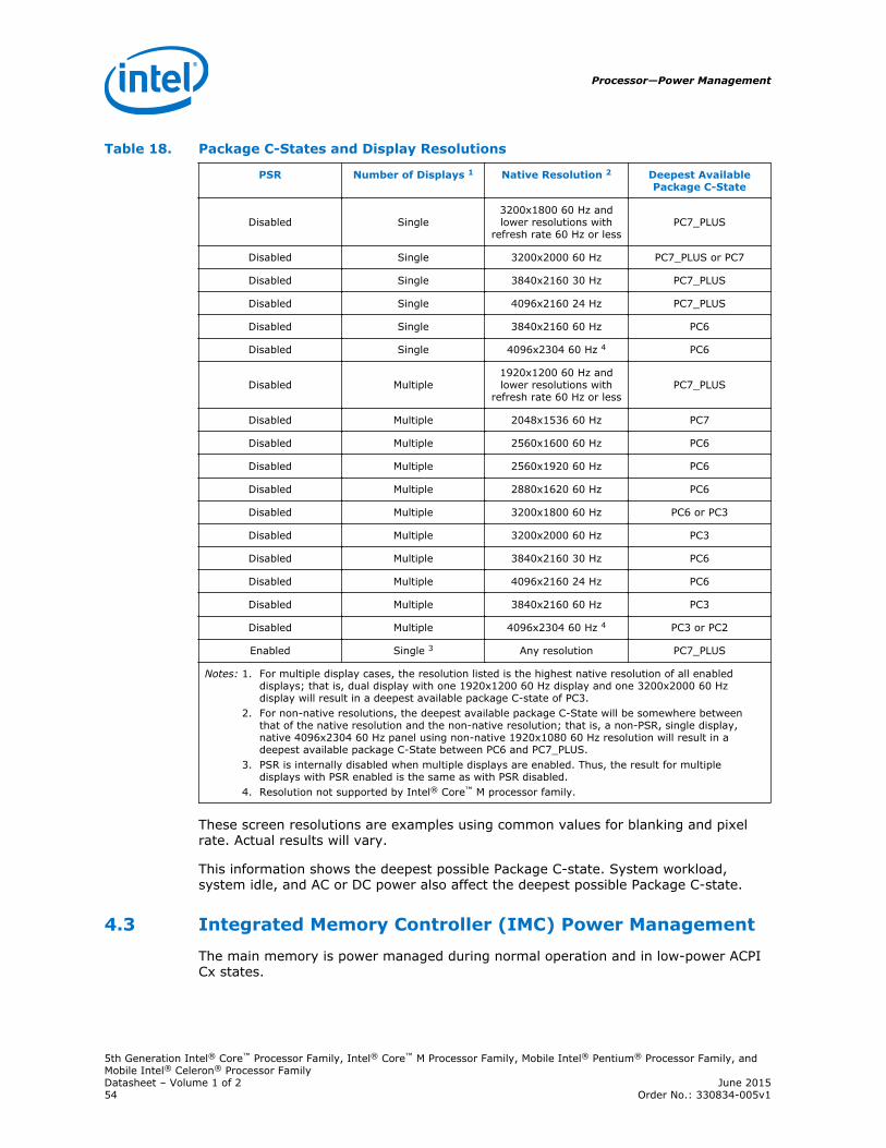
Table 18. Package C-States and Display Resolutions
PSR Number of Displays 1 Native Resolution 2 Deepest AvailablePackage C-State
Disabled Single3200x1800 60 Hz andlower resolutions with
refresh rate 60 Hz or lessPC7_PLUS
Disabled Single 3200x2000 60 Hz PC7_PLUS or PC7
Disabled Single 3840x2160 30 Hz PC7_PLUS
Disabled Single 4096x2160 24 Hz PC7_PLUS
Disabled Single 3840x2160 60 Hz PC6
Disabled Single 4096x2304 60 Hz 4 PC6
Disabled Multiple1920x1200 60 Hz andlower resolutions with
refresh rate 60 Hz or lessPC7_PLUS
Disabled Multiple 2048x1536 60 Hz PC7
Disabled Multiple 2560x1600 60 Hz PC6
Disabled Multiple 2560x1920 60 Hz PC6
Disabled Multiple 2880x1620 60 Hz PC6
Disabled Multiple 3200x1800 60 Hz PC6 or PC3
Disabled Multiple 3200x2000 60 Hz PC3
Disabled Multiple 3840x2160 30 Hz PC6
Disabled Multiple 4096x2160 24 Hz PC6
Disabled Multiple 3840x2160 60 Hz PC3
Disabled Multiple 4096x2304 60 Hz 4 PC3 or PC2
Enabled Single 3 Any resolution PC7_PLUS
Notes: 1. For multiple display cases, the resolution listed is the highest native resolution of all enableddisplays; that is, dual display with one 1920x1200 60 Hz display and one 3200x2000 60 Hzdisplay will result in a deepest available package C-state of PC3.
2. For non-native resolutions, the deepest available package C-State will be somewhere betweenthat of the native resolution and the non-native resolution; that is, a non-PSR, single display,native 4096x2304 60 Hz panel using non-native 1920x1080 60 Hz resolution will result in adeepest available package C-State between PC6 and PC7_PLUS.
3. PSR is internally disabled when multiple displays are enabled. Thus, the result for multipledisplays with PSR enabled is the same as with PSR disabled.
4. Resolution not supported by Intel® Core™ M processor family.
These screen resolutions are examples using common values for blanking and pixelrate. Actual results will vary.
This information shows the deepest possible Package C-state. System workload,system idle, and AC or DC power also affect the deepest possible Package C-state.
Integrated Memory Controller (IMC) Power Management
The main memory is power managed during normal operation and in low-power ACPICx states.
4.3
Processor—Power Management
5th Generation Intel® Core™ Processor Family, Intel® Core™ M Processor Family, Mobile Intel® Pentium® Processor Family, andMobile Intel® Celeron® Processor FamilyDatasheet – Volume 1 of 2 June 201554 Order No.: 330834-005v1
Disabling Unused System Memory Outputs
Any system memory (SM) interface signal that goes to a memory in which it is notconnected to any actual memory devices is tri-stated. The benefits of disabling unusedSM signals are:
• Reduced power consumption.
• Reduced possible overshoot/undershoot signal quality issues seen by theprocessor I/O buffer receivers caused by reflections from potentially un-terminated transmission lines.
When a given rank is not populated, the corresponding chip select and CKE signals arenot driven.
At reset, all rows must be assumed to be populated, until it can be determined thatthe rows are not populated. This is due to the fact that when CKE is tri-stated withDRAMs present, the DRAMs are not ensured to maintain data integrity. CKE tri-stateshould be enabled by BIOS where appropriate, since at reset all rows must beassumed to be populated.
CKE tri-state should be enabled by BIOS where appropriate, since at reset all rowsmust be assumed to be populated.
DRAM Power Management and Initialization
The processor implements extensive support for power management on the memoryinterface.The processor drives four CKE pins, one per rank.
The CKE is one of the power save means. When CKE is off, the internal DDR clock isdisabled and the DDR power is reduced. The power saving differs according to theselected mode and the DDR type used. For more information, refer to the IDD table inthe DDR specification.
The processor supports four different types of power-down modes in package C0. Thedifferent power-down modes can be enabled through configuring"PM_PDWN_config_0_0_0_MCHBAR". The type of CKE power-down can be configuredthrough PDWN_mode (bits 15:12) and the idle timer can be configured throughPDWN_idle_counter (bits 11:0). The different power-down modes supported are:
• No power-down (CKE disable)
• Active power-down (APD): This mode is entered if there are open pages whende-asserting CKE. In this mode the open pages are retained. Power-saving in thismode is the lowest. Power consumption of DDR is defined by IDD3P. Exiting thismode is defined by tXP – small number of cycles. For this mode, DRAM DLL mustbe on.
• PPD/DLL-off: In this mode the data-in DLLs on DDR are off. Power-saving in thismode is the best among all power modes. Power consumption is defined byIDD2P1. Exiting this mode is defined by tXP, but also tXPDLL (10–20 according toDDR type) cycles until first data transfer is allowed. For this mode, DRAM DLLmust be off.
• Pre-charged power-down (PPD): This mode is entered if all banks in DDR arepre-charged when de-asserting CKE. Power saving in this mode is intermediate –better than APD, but less than DLL-off. Power consumption is defined by IDD2P1.Exiting this mode is defined by tXP. The difference from APD mode is that when
4.3.1
4.3.2
Power Management—Processor
5th Generation Intel® Core™ Processor Family, Intel® Core™ M Processor Family, Mobile Intel® Pentium® Processor Family, andMobile Intel® Celeron® Processor Family
June 2015 Datasheet – Volume 1 of 2Order No.: 330834-005v1 55
waking-up all page-buffers are empty.) The LPDDR does not have a DLL. As aresult, the power savings are as good as PPD/DLL-off, but will have lower exitlatency and higher performance.
The CKE is determined per rank, whenever it is inactive. Each rank has an idle-counter. The idle-counter starts counting as soon as the rank has no accesses, and ifit expires, the rank may enter power-down while no new transactions to the rankarrives to queues. The idle-counter begins counting at the last incoming transactionarrival.
It is important to understand that since the power-down decision is per rank, the IMCcan find many opportunities to power down ranks, even while running memoryintensive applications; the savings are significant (may be few Watts, according to theDDR specification). This is significant when each channel is populated with moreranks.
Selection of power modes should be according to power-performance or thermaltrade-offs of a given system:
• When trying to achieve maximum performance and power or thermalconsideration is not an issue – use no power-down
• In a system which tries to minimize power-consumption, try using the deepestpower-down mode possible – PPD/DLL-off with a low idle timer value.
• In high-performance systems with dense packaging (that is, tricky thermaldesign) the power-down mode should be considered in order to reduce the heatingand avoid DDR throttling caused by the heating.
The default value that BIOS configures in "PM_PDWN_config_0_0_0_MCHBAR" is6080h; that is, PPD/DLL-off mode with idle timer of 80h, or 128 DCLKs. This is abalanced setting with deep power-down mode and moderate idle timer value.
The idle timer expiration count defines the number of DCKLs that a rank is idle thatcauses entry to the selected power mode. As this timer is set to a shorter time, theIMC will have more opportunities to put DDR in power-down. There is no BIOS hook toset this register. Customers choosing to change the value of this register can do it bychanging it in the BIOS. For experiments, this register can be modified in real time ifBIOS does not lock the IMC registers.
Initialization Role of CKE
During power-up, CKE is the only input to the SDRAM that has its level recognized(other than the DDR3L/DDR3L-RS reset pin) once power is applied. It must be drivenLOW by the DDR controller to make sure the SDRAM components float DQ and DQSduring power-up. CKE signals remain LOW (while any reset is active) until the BIOSwrites to a configuration register. Using this method, CKE is ensured to remaininactive for much longer than the specified 200 micro-seconds after power and clocksto SDRAM devices are stable.
Conditional Self-Refresh
During S0 idle state, system memory may be conditionally placed into self-refreshstate when the processor is in package C3 or deeper power state. Refer to Intel®Rapid Memory Power Management (Intel® RMPM) for more details on conditional self-refresh with Intel HD Graphics enabled.
4.3.2.1
4.3.2.2
Processor—Power Management
5th Generation Intel® Core™ Processor Family, Intel® Core™ M Processor Family, Mobile Intel® Pentium® Processor Family, andMobile Intel® Celeron® Processor FamilyDatasheet – Volume 1 of 2 June 201556 Order No.: 330834-005v1
When entering the S3 – Suspend-to-RAM (STR) state or S0 conditional self-refresh,the processor core flushes pending cycles and then enters SDRAM ranks that are notused by Intel graphics memory into self-refresh. The CKE signals remain LOW so theSDRAM devices perform self-refresh.
The target behavior is to enter self-refresh for package C3 or deeper power states aslong as there are no memory requests to service. The target usage is shown in thefollowing table.
Table 19. Targeted Memory State Conditions
Mode Memory State with Processor Graphics Memory State with External Graphics
C0, C1, C1E Dynamic memory rank power-down based onidle conditions.
Dynamic memory rank power-down based onidle conditions.
C3, C6, C7
If the processor graphics engine is idle andthere are no pending display requests, thenenter self-refresh. Otherwise, use dynamicmemory rank power-down based on idleconditions.
If there are no memory requests, then enterself-refresh. Otherwise, use dynamic memoryrank power-down based on idle conditions.
S3 Self-Refresh Mode Self-Refresh Mode
S4 Memory power-down (contents lost) Memory power-down (contents lost)
Dynamic Power-Down
Dynamic power-down of memory is employed during normal operation. Based on idleconditions, a given memory rank may be powered down. The IMC implementsaggressive CKE control to dynamically put the DRAM devices in a power-down state.The processor core controller can be configured to put the devices in active power-down (CKE de-assertion with open pages) or pre-charge power-down (CKE de-assertion with all pages closed). Pre-charge power-down provides greater powersavings, but has a bigger performance impact since all pages will first be closed beforeputting the devices in power-down mode.
If dynamic power-down is enabled, all ranks are powered up before doing a refreshcycle and all ranks are powered down at the end of refresh.
DRAM I/O Power Management
Unused signals should be disabled to save power and reduce electromagneticinterference. This includes all signals associated with an unused memory channel.Clocks, CKE, ODE, and CS signals are controlled per DIMM rank and will be powereddown for unused ranks.
The I/O buffer for an unused signal should be tri-stated (output driver disabled), theinput receiver (differential sense-amp) should be disabled, and any DLL circuitryrelated ONLY to unused signals should be disabled. The input path must be gated toprevent spurious results due to noise on the unused signals (typically handledautomatically when input receiver is disabled).
DDR Electrical Power Gating (EPG)
The DDR I/O of the processor supports Electrical Power Gating (DDR-EPG) while theprocessor is at C3 or deeper power state.
4.3.2.3
4.3.2.4
4.3.3
Power Management—Processor
5th Generation Intel® Core™ Processor Family, Intel® Core™ M Processor Family, Mobile Intel® Pentium® Processor Family, andMobile Intel® Celeron® Processor Family
June 2015 Datasheet – Volume 1 of 2Order No.: 330834-005v1 57
In C3 or deeper power state, the processor internally gates VDDQ for the majority ofthe logic to reduce idle power while keeping all critical DDR pins such as CKE andVREF in the appropriate state.
In C7 or deeper power state, the processor internally gates VccST for all non-criticalstate to reduce idle power.
In S3 or C-state transitions, the DDR does not go through training mode and willrestore the previous training information.
Graphics Power Management
Intel® Rapid Memory Power Management (Intel® RMPM)
Intel Rapid Memory Power Management (Intel RMPM) conditionally places memoryinto self-refresh when the processor is in package C3 or deeper power state to allowthe system to remain in the lower power states longer for memory not reserved forgraphics memory. Intel RMPM functionality depends on graphics/display state(relevant only when processor graphics is being used), as well as memory trafficpatterns generated by other connected I/O devices.
Graphics Render C-State
Render C-state (RC6) is a technique designed to optimize the average power to thegraphics render engine during times of idleness. RC6 is entered when the graphicsrender engine, blitter engine, and the video engine have no workload being currentlyworked on and no outstanding graphics memory transactions. When the idlenesscondition is met, the processor graphics will program the graphics render engineinternal power rail into a low voltage state.
Intel® Smart 2D Display Technology (Intel® S2DDT)
Intel S2DDT reduces display refresh memory traffic by reducing memory readsrequired for display refresh. Power consumption is reduced by less accesses to theIMC. Intel S2DDT is only enabled in single pipe mode.
Intel S2DDT is most effective with:
• Display images well suited to compression, such as text windows, slide shows, andso on. Poor examples are 3D games.
• Static screens such as screens with significant portions of the background showing2D applications, processor benchmarks, and so on, or conditions when theprocessor is idle. Poor examples are full-screen 3D games and benchmarks thatflip the display image at or near display refresh rates.
Intel® Graphics Dynamic Frequency
Intel Graphics Dynamic Frequency Technology is the ability of the processor andgraphics cores to opportunistically increase frequency and/or voltage above theguaranteed processor and graphics frequency for the given part. Intel GraphicsDynamic Frequency Technology is a performance feature that makes use of unusedpackage power and thermals to increase application performance. The increase infrequency is determined by how much power and thermal budget is available in thepackage, and the application demand for additional processor or graphics
4.4
4.4.1
4.4.2
4.4.3
4.4.4
Processor—Power Management
5th Generation Intel® Core™ Processor Family, Intel® Core™ M Processor Family, Mobile Intel® Pentium® Processor Family, andMobile Intel® Celeron® Processor FamilyDatasheet – Volume 1 of 2 June 201558 Order No.: 330834-005v1
performance. The processor core control is maintained by an embedded controller.The graphics driver dynamically adjusts between P-States to maintain optimalperformance, power, and thermals. The graphics driver will always try to place thegraphics engine in the most energy efficient P-state.
Intel® Display Power Saving Technology (Intel® DPST)
The Intel DPST technique achieves backlight power savings while maintaining a goodvisual experience. This is accomplished by adaptively enhancing the displayed imagewhile decreasing the backlight brightness simultaneously. The goal of this technique isto provide equivalent end-user-perceived image quality at a decreased backlightpower level.
1. The original (input) image produced by the operating system or application isanalyzed by the Intel DPST subsystem. An interrupt to Intel DPST software isgenerated whenever a meaningful change in the image attributes is detected. (Ameaningful change is when the Intel DPST software algorithm determines thatenough brightness, contrast, or color change has occurred to the displayingimages that the image enhancement and backlight control needs to be altered.)
2. Intel DPST subsystem applies an image-specific enhancement to increase imagecontrast, brightness, and other attributes.
3. A corresponding decrease to the backlight brightness is applied simultaneously toproduce an image with similar user-perceived quality (such as brightness) as theoriginal image.
Intel DPST 6.0 has improved the software algorithms and has minor hardwarechanges to better handle backlight phase-in and ensures the documented andvalidated method to interrupt hardware phase-in.
Intel® Automatic Display Brightness
The Intel Automatic Display Brightness feature dynamically adjusts the backlightbrightness based upon the current ambient light environment. This feature requires anadditional sensor to be on the panel front. The sensor receives the changing ambientlight conditions and sends the interrupts to the Intel Graphics driver. As per thechange in Lux, (current ambient light illuminance), the new backlight setting can beadjusted through BLC. The converse applies for a brightly lit environment. IntelAutomatic Display Brightness increases the backlight setting.
Intel® Seamless Display Refresh Rate Technology (Intel®SDRRS Technology)
When a Local Flat Panel (LFP) supports multiple refresh rates, the Intel DisplayRefresh Rate Switching power conservation feature can be enabled. The higher refreshrate will be used when plugged in with an AC power adaptor or when the end user hasnot selected/enabled this feature. The graphics software will automatically switch to alower refresh rate for maximum battery life when the notebook is on battery powerand when the user has selected/enabled this feature. There are two distinctimplementations of Intel DRRS – static and seamless. The static Intel DRRS methoduses a mode change to assign the new refresh rate. The seamless Intel DRRS methodis able to accomplish the refresh rate assignment without a mode change andtherefore does not experience some of the visual artifacts associated with the modechange (SetMode) method.
4.4.5
4.4.6
4.4.7
Power Management—Processor
5th Generation Intel® Core™ Processor Family, Intel® Core™ M Processor Family, Mobile Intel® Pentium® Processor Family, andMobile Intel® Celeron® Processor Family
June 2015 Datasheet – Volume 1 of 2Order No.: 330834-005v1 59
5.0 Thermal Management
The thermal solution provides both component-level and system-level thermalmanagement. To allow for the optimal operation and long-term reliability of Intelprocessor-based systems, the system/processor thermal solution should be designedso that the processor:
• Remains below the maximum junction temperature (TjMax) specification at themaximum thermal design power (TDP).
• Conforms to system constraints, such as system acoustics, system skin-temperatures, and exhaust-temperature requirements.
Caution: Thermal specifications given in this chapter are on the component andpackage level and apply specifically to the processor. Operating the processor outsidethe specified limits may result in permanent damage to the processor and potentiallyother components in the system.
Thermal Considerations
The processor TDP is the maximum sustained power that should be used for design ofthe processor thermal solution. TDP is a power dissipation and junction temperatureoperating condition limit specified in this document; that is validated duringmanufacturing for the base configuration when executing a near worst casecommercially available workload as specified by Intel for the SKU segment. TDP maybe exceeded for short periods of time or if running a "power virus" workload.
The processor integrates multiple processing and graphics cores and PCH on a singlepackage.This may result in differences in the power distribution across the die andmust be considered when designing the thermal solution.
Intel® Turbo Boost Technology 2.0 allows processor cores and processor graphicscores to run faster than the guaranteed frequency. It is invoked opportunistically andautomatically as long as the processor is conforming to its temperature, powerdelivery, and current specification limits. When Intel Turbo Boost Technology 2.0 isenabled:
• Applications are expected to run closer to TDP more often as the processor willattempt to maximize performance by taking advantage of available TDP headroomin the processor package.
• The processor may exceed the TDP for short durations to use any availablethermal capacitance within the thermal solution. The duration and time of suchoperation can be limited by platform runtime configurable registers within theprocessor.
• Thermal solutions and platform cooling that are designed to less than thermaldesign guidance may experience thermal and performance issues since moreapplications will tend to run at or near TDP for significant periods of time.
Note: Intel Turbo Boost Technology 2.0 availability may vary between the different SKUs.
5.1
Processor—Thermal Management
5th Generation Intel® Core™ Processor Family, Intel® Core™ M Processor Family, Mobile Intel® Pentium® Processor Family, andMobile Intel® Celeron® Processor FamilyDatasheet – Volume 1 of 2 June 201560 Order No.: 330834-005v1
Intel® Turbo Boost Technology 2.0 Power Monitoring
When operating in turbo mode, the processor monitors its own power and adjusts theturbo frequencies to maintain the average power within limits over a thermallysignificant time period. The processor calculates the package power that consists ofthe processor core power and graphics core power. In the event that a workloadcauses the power to exceed program power limits, the processor will protect itselfusing the Adaptive Thermal Monitor.
Intel® Turbo Boost Technology 2.0 Power Control
Illustration of Intel Turbo Boost Technology 2.0 power control is shown in thefollowing sections and figures. Multiple controls operate simultaneously allowing forcustomization for multiple system thermal and power limitations. These controls allowfor turbo optimizations within system constraints and are accessible using MSR, MMIO,or PECI interfaces.
Package Power Control
The package power control settings of PL1, PL2, and PL3 Tau allow the designer toconfigure Intel Turbo Boost Technology 2.0 to match the platform power delivery andpackage thermal solution limitations.
• Power Limit 1 (PL1): A threshold for average power that will not exceed;recommend to set equal to TDP power. PL1 should not be set higher than thermalsolution cooling limits.
• Power Limit 2 (PL2): A threshold that if exceeded, the PL2 rapid power limitingalgorithms will attempt to limit the spike above PL2.
• Power Limit 3 (PL3): A threshold that if exceeded, the PL3 rapid power limitingalgorithms will attempt to limit the duty cycle of spikes above PL3 by reactivelylimiting frequency. This is an optional setting.
• Turbo Time Parameter (Tau): An averaging constant used for PL1 exponentialweighted moving average (EWMA) power calculation.
Notes: 1. Implementation of Intel Turbo Boost Technology 2.0 only requires configuring PL1,PL1 Tau, and PL2.
2. PL3 is disabled by default.
5.2
5.3
5.3.1
Thermal Management—Processor
5th Generation Intel® Core™ Processor Family, Intel® Core™ M Processor Family, Mobile Intel® Pentium® Processor Family, andMobile Intel® Celeron® Processor Family
June 2015 Datasheet – Volume 1 of 2Order No.: 330834-005v1 61

Figure 12. Package Power Control
Turbo Time Parameter
Turbo Time Parameter is a mathematical parameter (units in seconds) that controlsthe Intel Turbo Boost Technology 2.0 algorithm using moving average of energyusage. During a maximum power turbo event of about 1.25 x TDP, the processorcould sustain PL2 for up to approximately 1.5 times the Turbo Time Parameter. If thepower value and/or Turbo Time Parameter is changed during runtime, it may takeapproximately 3 to 5 times the Turbo Time Parameter for the algorithm to settle at thenew control limits. The time varies depending on the magnitude of the change andother factors. There is an individual Turbo Time Parameter associated with PackagePower Control.
Configurable TDP (cTDP) and Low-Power Mode
Configurable TDP (cTDP) and Low-Power Mode (LPM) form a design vector where theprocessor's behavior and package TDP are dynamically adjusted to a desired systemperformance and power envelope. Configurable TDP and Low-Power Modetechnologies offer opportunities to differentiate system design while running activeworkloads on select processor SKUs through scalability, configuration and adaptability.The scenarios or methods by which each technology is used are customizable buttypically involve changes to PL1 and associated frequencies for the scenario with aresultant change in performance depending on system's usage. Either technology canbe triggered by (but are not limited to) changes in OS power policies or hardwareevents such as docking a system, flipping a switch or pressing a button. cTDP and LPMare designed to be configured dynamically and do not require an operating systemreboot.
Note: Configurable TDP and Low-Power Mode technologies are not battery life improvementtechnologies.
5.3.2
5.4
Processor—Thermal Management
5th Generation Intel® Core™ Processor Family, Intel® Core™ M Processor Family, Mobile Intel® Pentium® Processor Family, andMobile Intel® Celeron® Processor FamilyDatasheet – Volume 1 of 2 June 201562 Order No.: 330834-005v1
Configurable TDP
Note: Configurable TDP availability may vary between the different SKUs.
With cTDP, the processor is now capable of altering the maximum sustained powerwith an alternate IA core base frequency. Configurable TDP allows operation insituations where extra cooling is available or situations where a cooler and quietermode of operation is desired. Configurable TDP can be enabled using Intel's DPTFdriver or through HW/EC firmware. Enabling cTDP using the DPTF driver isrecommended as Intel does not provide specific application or EC source code.
cTDP consists of three modes as shown in the following table.
Table 20. Configurable TDP Modes
Mode Description
Base
The average power dissipation and junction temperature operating condition limit forwhich the processor is validated during manufacturing when executing an associatedIntel-specified high-complexity workload at the processor IA core frequencycorresponding to the configuration and SKU.
TDP-Up
The SKU-specific processor IA core frequency where manufacturing confirms logicalfunctionality within the set of operating condition limits specified for the SKU segmentand Configurable TDP-Up configuration. The Configurable TDP-Up Frequency andcorresponding TDP is higher than the processor IA core Base Frequency and SKUSegment Base TDP.
TDP-Down
The processor IA core frequency where manufacturing confirms logical functionalitywithin the set of operating condition limits specified for the SKU segment andConfigurable TDP-Down configuration. The Configurable TDP-Down Frequency andcorresponding TDP is lower than the processor IA core Base Frequency and SKUSegment Base TDP.
In each mode, the Intel Turbo Boost Technology 2.0 power and frequency ranges arereprogrammed and the OS is given a new effective HFM operating point. The IntelDPTF driver assists in all these operations. The cTDP mode does not change the maxper-core turbo frequency.
Low-Power Mode
Low-Power Mode (LPM) can provide cooler and quieter system operation. Bycombining several active power limiting techniques, the processor can consume lesspower while running at equivalent low frequencies. Active power is defined asprocessor power consumed while a workload is running and does not refer to thepower consumed during idle modes of operation. LPM is only available using the IntelDPTF driver.
Through the DPTF driver, LPM can be configured to use each of the following methodsto reduce active power:
• Restricting Intel Turbo Boost Power limits and IA core Turbo Boost availability
• Off-Lining core activity (Move processor traffic to a subset of cores)
• Placing an IA Core at LFM or LSF (Lowest Supported Frequency)
• Utilizing IA clock modulation
• Reducing number of active EUs to GT2 equivalent (Applicable for GT3 SKUs Only)
• LPM power as listed in the TDP Specifications table is defined at a point which IAcores are working at MFM, GT = RPn and 1 core active
5.4.1
5.4.2
Thermal Management—Processor
5th Generation Intel® Core™ Processor Family, Intel® Core™ M Processor Family, Mobile Intel® Pentium® Processor Family, andMobile Intel® Celeron® Processor Family
June 2015 Datasheet – Volume 1 of 2Order No.: 330834-005v1 63
Off-lining core activity is the ability to dynamically scale a workload to a limited subsetof cores in conjunction with a lower turbo power limit. It is one of the main vectorsavailable to reduce active power. However, not all processor activity is ensured to beable to shift to a subset of cores. Shifting a workload to a limited subset of coresallows other cores to remain idle and save power. Therefore, when LPM is enabled,less power is consumed at equivalent frequencies.
Minimum Frequency Mode (MFM) of operation, which is the lowest supportedfrequency (LSF) at the LFM voltage, has been made available for use under LPM forfurther reduction in active power beyond LFM capability to enable cooler and quietermodes of operation.
Thermal and Power Specifications
The following notes apply to Table 22 on page 65 .
Note Definition
1
The TDP and Configurable TDP values are the average power dissipation in junction temperature operatingcondition limit, for the SKU Segment and Configuration, for which the processor is validated during manufacturingwhen executing an associated Intel-specified high-complexity workload at the processor IA core frequencycorresponding to the configuration and SKU.
2 TDP workload may consist of a combination of processor-core intensive and graphics-core intensive applications.
3 The thermal solution needs to ensure that the processor temperature does not exceed the maximum junctiontemperature (TjMAX) limit, as measured by the DTS and the critical temperature bit.
4 The processor junction temperature is monitored by Digital Temperature Sensors (DTS). For DTS accuracy, refer to Digital Thermal Sensor Accuracy (Taccuracy) on page 69.
5 At Tj of TjMAX
6 Can be modified at runtime by MSR writes, with MMIO and with PECI commands.
7'Turbo Time Parameter' is a mathematical parameter (unit in seconds) that controls the processor turbo algorithmusing a moving average of energy usage. Do not set the Turbo Time Parameter to a value less than 0.1 seconds.Refer to Turbo Time Parameter on page 62 for further information.
8 Shown limit is a time averaged power, based upon the Turbo Time Parameter. Absolute product power may exceedthe set limits for short durations or under virus or uncharacterized workloads.
9
Processor will be controlled to specified power limit as described in Intel Turbo Boost Technology 2.0 PowerMonitoring on page 61. If the power value and/or 'Turbo Time Parameter' is changed during runtime, it may take ashort period of time (approximately 3 to 5 times the 'Turbo Time Parameter') for the algorithm to settle at the newcontrol limits.
10 This is a hardware default setting and not a behavioral characteristic of the part.
11 For controllable turbo workloads, limit may be exceeded for up to 10 ms.
12 Refer to Table 20 on page 63 for the definitions of 'base', 'TDP-Up' and 'TDP-Down'.
13 LPM power level is an opportunistic power and is not a guaranteed value as usages and implementations may vary.
14 Power limits may vary depending on if the product supports the 'TDP-up' and/or 'TDP-down' modes. Default powerlimits can be found in the PKG_PWR_SKU MSR (614h).
15 May vary based on SKU.
16 Hardware default values might be overridden by the BIOS.
5.5
Processor—Thermal Management
5th Generation Intel® Core™ Processor Family, Intel® Core™ M Processor Family, Mobile Intel® Pentium® Processor Family, andMobile Intel® Celeron® Processor FamilyDatasheet – Volume 1 of 2 June 201564 Order No.: 330834-005v1
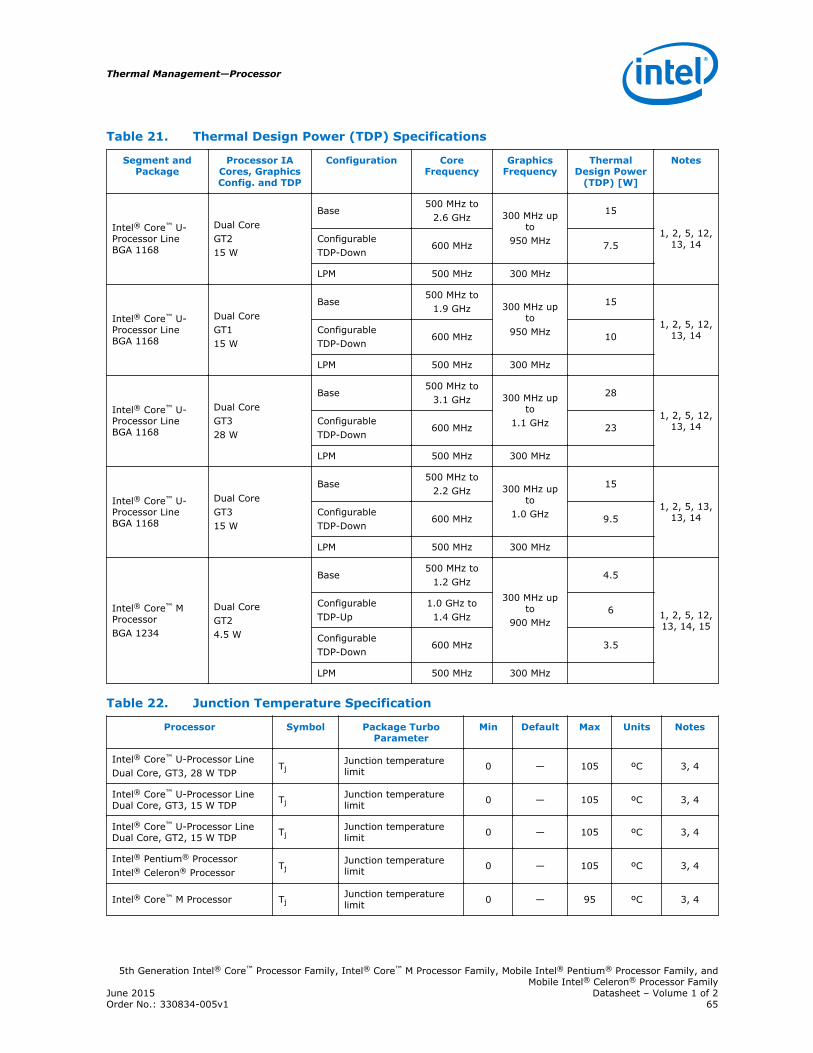
Table 21. Thermal Design Power (TDP) Specifications
Segment andPackage
Processor IACores, GraphicsConfig. and TDP
Configuration CoreFrequency
GraphicsFrequency
ThermalDesign Power
(TDP) [W]
Notes
Intel® Core™ U-Processor LineBGA 1168
Dual CoreGT215 W
Base500 MHz to
2.6 GHz 300 MHz upto
950 MHz
15
1, 2, 5, 12,13, 14Configurable
TDP-Down600 MHz 7.5
LPM 500 MHz 300 MHz
Intel® Core™ U-Processor LineBGA 1168
Dual CoreGT115 W
Base500 MHz to
1.9 GHz 300 MHz upto
950 MHz
15
1, 2, 5, 12,13, 14Configurable
TDP-Down600 MHz 10
LPM 500 MHz 300 MHz
Intel® Core™ U-Processor LineBGA 1168
Dual CoreGT328 W
Base500 MHz to
3.1 GHz 300 MHz upto
1.1 GHz
28
1, 2, 5, 12,13, 14Configurable
TDP-Down600 MHz 23
LPM 500 MHz 300 MHz
Intel® Core™ U-Processor LineBGA 1168
Dual CoreGT315 W
Base500 MHz to
2.2 GHz 300 MHz upto
1.0 GHz
15
1, 2, 5, 13,13, 14Configurable
TDP-Down600 MHz 9.5
LPM 500 MHz 300 MHz
Intel® Core™ MProcessorBGA 1234
Dual CoreGT24.5 W
Base500 MHz to
1.2 GHz300 MHz up
to900 MHz
4.5
1, 2, 5, 12,13, 14, 15
ConfigurableTDP-Up
1.0 GHz to1.4 GHz
6
ConfigurableTDP-Down
600 MHz 3.5
LPM 500 MHz 300 MHz
Table 22. Junction Temperature Specification
Processor Symbol Package TurboParameter
Min Default Max Units Notes
Intel® Core™ U-Processor LineDual Core, GT3, 28 W TDP
TjJunction temperaturelimit 0 — 105 ºC 3, 4
Intel® Core™ U-Processor LineDual Core, GT3, 15 W TDP Tj
Junction temperaturelimit 0 — 105 ºC 3, 4
Intel® Core™ U-Processor LineDual Core, GT2, 15 W TDP Tj
Junction temperaturelimit 0 — 105 ºC 3, 4
Intel® Pentium® ProcessorIntel® Celeron® Processor
TjJunction temperaturelimit 0 — 105 ºC 3, 4
Intel® Core™ M Processor TjJunction temperaturelimit 0 — 95 ºC 3, 4
Thermal Management—Processor
5th Generation Intel® Core™ Processor Family, Intel® Core™ M Processor Family, Mobile Intel® Pentium® Processor Family, andMobile Intel® Celeron® Processor Family
June 2015 Datasheet – Volume 1 of 2Order No.: 330834-005v1 65

Table 23. Idle Power Specification
Symbol Parameter Min Typical Max Unit Note
PPACKAGE(C6) Package power in Package C6 state — — 0.6 W 1, 2
PPACKAGE(C7) Package power in Package C7 state — — 0.4 W 1, 2
PPACKAGE(C9) Package power in Package C9 state — — 0.03 W 1, 2
PPACKAGE(C10) Package power in Package C10 state — — 0.03 W 1, 2
Notes: 1. Package power includes both components in the processor package: processor and PCH.2. The power specification based on pre-silicon estimations, and may be subject to change.3. Measured at Tj = 35 °C.4. The idle power specifications are not 100% tested. These power specifications are determined by the
characterization at higher temperatures and extrapolating the values for the junction temperature indicated.
Thermal Management Features
Occasionally the processor may operate in conditions that are near to its maximumoperating temperature. This can be due to internal overheating or overheating withinthe platform. To protect the processor and the platform from thermal failure, severalthermal management features exist to reduce package power consumption andthereby temperature in order to remain within normal operating limits. Furthermore,the processor supports several methods to reduce memory power.
Adaptive Thermal Monitor
The purpose of the Adaptive Thermal Monitor is to reduce processor core powerconsumption and temperature until it operates at or below its maximum operatingtemperature. Processor core power reduction is achieved by:
• Adjusting the operating frequency (using the core ratio multiplier) and voltage.
• Modulating (starting and stopping) the internal processor core clocks (duty cycle).
The Adaptive Thermal Monitor can be activated when the package temperature,monitored by any digital thermal sensor (DTS) meets or exceeds its maximumoperating temperature. The maximum operating temperature implies either maximumjunction temperature TjMAX, or TjMAX minus TCC Activation offset.
Exceeding the maximum operating temperature activates the thermal control circuit(TCC), if enabled. When activated, the thermal control circuit (TCC) causes both theprocessor core and graphics core to reduce frequency and voltage adaptively. TheAdaptive Thermal Monitor will remain active as long as the package temperatureexceeds its specified limit. Therefore, the Adaptive Thermal Monitor will continue toreduce the package frequency and voltage until the TCC is de-activated.
TjMAX is factory calibrated and is not user configurable. The default value is softwarevisible in the TEMPERATURE_TARGET (0x1A2) MSR, bits [23:16]. TheTEMPERATURE_TARGET value stays the same when TCC Activation offset is enabled.
The Adaptive Thermal Monitor does not require any additional hardware, softwaredrivers, or interrupt handling routines. It is not intended as a mechanism to maintainprocessor TDP. The system design should provide a thermal solution that can maintainTDP within its intended usage range.
Note: Adaptive Thermal Monitor protection is always enabled.
5.6
5.6.1
Processor—Thermal Management
5th Generation Intel® Core™ Processor Family, Intel® Core™ M Processor Family, Mobile Intel® Pentium® Processor Family, andMobile Intel® Celeron® Processor FamilyDatasheet – Volume 1 of 2 June 201566 Order No.: 330834-005v1
Thermal Control Circuit (TCC) Activation Offset
TCC Activation Offset can be used to activate the Adaptive Thermal Monitor attemperatures lower than TjMAX. It is the preferred thermal protection mechanism forIntel Turbo Boost Technology 2.0 operation since ACPI passive throttling states willpull the processor out of turbo mode operation when triggered. An offset (in degreesCelsius) can be written to the TEMPERATURE_TARGET (0x1A2) MSR, bits [29:24]. Thisvalue will be subtracted from the value found in bits [23:16]. The default offset is0 °C, TCC activation will occur at TjMAX. The offset should be set lower than any otherprotection such as ACPI _PSV trip points.
Frequency / Voltage Control
Upon Adaptive Thermal Monitor activation, the processor core attempts to dynamicallyreduce processor core power by lowering the frequency and voltage operating point.The operating points are automatically calculated by the processor core itself and donot require the BIOS to program them as with previous generations of Intelprocessors. The processor core will scale the operating points such that:
• The voltage will be optimized according to the temperature, the core bus ratio,and number of cores in deep C-states.
• The core power and temperature are reduced while minimizing performancedegradation.
Once the temperature has dropped below the maximum operating temperature, theoperating frequency and voltage will transition back to the normal system operatingpoint.
Once a target frequency/bus ratio is resolved, the processor core will transition to thenew target automatically.
• On an upward operating point transition, the voltage transition precedes thefrequency transition.
• On a downward transition, the frequency transition precedes the voltagetransition.
• The processor continues to execute instructions. However, the processor will haltinstruction execution for frequency transitions.
If a processor load-based Enhanced Intel SpeedStep Technology/P-state transition(through MSR write) is initiated while the Adaptive Thermal Monitor is active, thereare two possible outcomes:
• If the P-state target frequency is higher than the processor core optimized targetfrequency, the P-state transition will be deferred until the thermal event has beencompleted.
• If the P-state target frequency is lower than the processor core optimized targetfrequency, the processor will transition to the P-state operating point.
Clock Modulation
If the frequency/voltage changes are unable to end an Adaptive Thermal Monitorevent, the Adaptive Thermal Monitor will utilize clock modulation. Clock modulation isdone by alternately turning the clocks off and on at a duty cycle (ratio between clock"on" time and total time) specific to the processor. The duty cycle is factory configuredto 25% on and 75% off and cannot be modified. The period of the duty cycle isconfigured to 32 microseconds when the Adaptive Thermal Monitor is active. Cycle
5.6.1.1
5.6.1.2
5.6.1.3
Thermal Management—Processor
5th Generation Intel® Core™ Processor Family, Intel® Core™ M Processor Family, Mobile Intel® Pentium® Processor Family, andMobile Intel® Celeron® Processor Family
June 2015 Datasheet – Volume 1 of 2Order No.: 330834-005v1 67
times are independent of processor frequency. A small amount of hysteresis has beenincluded to prevent excessive clock modulation when the processor temperature isnear its maximum operating temperature. Once the temperature has dropped belowthe maximum operating temperature and the hysteresis timer has expired, theAdaptive Thermal Monitor goes inactive and clock modulation ceases. Clockmodulation is automatically engaged as part of the Adaptive Thermal Monitoractivation when the frequency/voltage targets are at their minimum settings.Processor performance will be decreased by the same amount as the duty cycle whenclock modulation is active. Snooping and interrupt processing are performed in thenormal manner while the Adaptive Thermal Monitor is active.
Digital Thermal Sensor
Each processor execution core has an on-die Digital Thermal Sensor (DTS) thatdetects the core's instantaneous temperature. The DTS is the preferred method ofmonitoring processor die temperature because:
• It is located near the hottest portions of the die.
• It can accurately track the die temperature and ensure that the Adaptive ThermalMonitor is not excessively activated.
Temperature values from the DTS can be retrieved through:
• A software interface using processor Model Specific Register (MSR).
• A processor hardware interface as described in Platform Environmental ControlInterface (PECI) on page 31.
When temperature is retrieved by the processor MSR, it is the instantaneoustemperature of the given core. When temperature is retrieved using PECI, it is theaverage of the highest DTS temperature in the package over a 256 ms time window.Intel recommends using the PECI reported temperature for platform thermal controlthat benefits from averaging, such as fan speed control. The average DTStemperature may not be a good indicator of package Adaptive Thermal Monitoractivation or rapid increases in temperature that triggers the Out of Specificationstatus bit within the PACKAGE_THERM_STATUS MSR 1B1h and IA32_THERM_STATUSMSR 19Ch.
Code execution is halted in C1 or deeper C-states. Package temperature can still bemonitored through PECI in lower C-states.
Unlike traditional thermal devices, the DTS outputs a temperature relative to themaximum supported operating temperature of the processor (TjMAX), regardless ofTCC activation offset. It is the responsibility of software to convert the relativetemperature to an absolute temperature. The absolute reference temperature isreadable in the TEMPERATURE_TARGET MSR 1A2h. The temperature returned by theDTS is an implied negative integer indicating the relative offset from TjMAX. The DTSdoes not report temperatures greater than TjMAX. The DTS-relative temperaturereadout directly impacts the Adaptive Thermal Monitor trigger point. When a packageDTS indicates that it has reached the TCC activation (a reading of 0h, except when theTCC activation offset is changed), the TCC will activate and indicate an AdaptiveThermal Monitor event. A TCC activation will lower both IA core and graphics corefrequency, voltage, or both. Changes to the temperature can be detected using twoprogrammable thresholds located in the processor thermal MSRs. These thresholdshave the capability of generating interrupts using the core's local APIC. Refer to theIntel® 64 and IA-32 Architectures Software Developer’s Manual for specific registerand programming details.
5.6.2
Processor—Thermal Management
5th Generation Intel® Core™ Processor Family, Intel® Core™ M Processor Family, Mobile Intel® Pentium® Processor Family, andMobile Intel® Celeron® Processor FamilyDatasheet – Volume 1 of 2 June 201568 Order No.: 330834-005v1
Digital Thermal Sensor Accuracy (Taccuracy)
The DTS is expected to work within ±5° C over the operating range.
Fan Speed Control with Digital Thermal Sensor
Digital Thermal Sensor based fan speed control (TFAN) is a recommended feature toachieve optimal thermal performance. At the TFAN temperature, Intel recommends fullcooling capability well before the DTS reading reaches TjMAX.
PROCHOT# Signal
PROCHOT# (processor hot) is asserted when the processor temperature has reachedits maximum operating temperature (TjMAX). Only a single PROCHOT# pin exists at apackage level. When any core arrives at the TCC activation point, the PROCHOT#signal will be asserted. PROCHOT# assertion policies are independent of AdaptiveThermal Monitor enabling.
Bi-Directional PROCHOT#
By default, the PROCHOT# signal is set to bi-directional. However, it is recommendedto configure the signal as an input only. When configured as an input or bi-directionalsignal, PROCHOT# can be used for thermally protecting other platform components incase the components overheat as well. When PROCHOT# is driven by an externaldevice:
• The package will immediately transition to the lowest P-State (Pn) supported bythe processor and graphics cores. This is contrary to the internally-generatedAdaptive Thermal Monitor response.
• Clock modulation is not activated.
The processor package will remain at the lowest supported P-state until the systemde-asserts PROCHOT#. The processor can be configured to generate an interrupt uponassertion and de-assertion of the PROCHOT# signal.
Note: When PROCHOT# is configured as a bi-directional signal and PROCHOT# is assertedby the processor, it is impossible for the processor to detect a system assertion ofPROCHOT#. The system assertion will have to wait until the processor de-assertsPROCHOT# before PROCHOT# action can occur due to the system assertion. While theprocessor is hot and asserting PROCHOT#, the power is reduced; however, thereduction rate is slower than the system PROCHOT# response of < 100 us. Theprocessor thermal control is staged in smaller increments over many milliseconds. Thismay cause several milliseconds of delay to a system assertion of PROCHOT# while theoutput function is asserted.
Voltage Regulator Protection using PROCHOT#
PROCHOT# may be used for thermal protection of voltage regulators (VR). Systemdesigners can create a circuit to monitor the VR temperature and assert PROCHOT#and, if enabled, activate the TCC when the temperature limit of the VR is reached.When PROCHOT# is configured as a bi-directional or input only signal, if the systemassertion of PROCHOT# is recognized by the processor, it will result in an immediatetransition to the lowest P-State (Pn) supported by the processor and graphics cores.Systems should still provide proper cooling for the VR and rely on bi-directional
5.6.2.1
5.6.2.2
5.6.3
5.6.3.1
5.6.3.2
Thermal Management—Processor
5th Generation Intel® Core™ Processor Family, Intel® Core™ M Processor Family, Mobile Intel® Pentium® Processor Family, andMobile Intel® Celeron® Processor Family
June 2015 Datasheet – Volume 1 of 2Order No.: 330834-005v1 69
PROCHOT# only as a backup in case of system cooling failure. Overall, the systemthermal design should allow the power delivery circuitry to operate within itstemperature specification even while the processor is operating at its TDP.
Thermal Solution Design and PROCHOT# Behavior
With a properly designed and characterized thermal solution, it is anticipated thatPROCHOT# will only be asserted for very short periods of time when running the mostpower intensive applications. The processor performance impact due to these briefperiods of TCC activation is expected to be so minor that it would be immeasurable.However, an under-designed thermal solution that is not able to prevent excessiveassertion of PROCHOT# in the anticipated ambient environment may:
• Cause a noticeable performance loss.
• Result in prolonged operation at or above the specified maximum junctiontemperature and affect the long-term reliability of the processor.
• May be incapable of cooling the processor even when the TCC is activecontinuously (in extreme situations).
Low-Power States and PROCHOT# Behavior
Depending on package power levels during package C-states, outbound PROCHOT#may de-assert while the processor is idle as power is removed from the signal. Uponwakeup, if the processor is still hot, the PROCHOT# will re-assert, although typicallypackage idle state residency should resolve any thermal issues. The PECI interface isfully operational during all C-states and it is expected that the platform continues tomanage processor core and package thermals even during idle states by regularlypolling for thermal data over PECI.
THERMTRIP# Signal
Regardless of enabling the automatic or on-demand modes, in the event of acatastrophic cooling failure, the package will automatically shut down when the siliconhas reached an elevated temperature that risks physical damage to the product. Atthis point the THERMTRIP# signal will go active.
Critical Temperature Detection
Critical Temperature detection is performed by monitoring the package temperature.This feature is intended for graceful shutdown before the THERMTRIP# is activated.However, the processor execution is not guaranteed between critical temperature andTHERMTRIP#. If the Adaptive Thermal Monitor is triggered and the temperatureremains high, a critical temperature status and sticky bit are latched in thePACKAGE_THERM_STATUS MSR 1B1h and the condition also generates a thermalinterrupt, if enabled. For more details on the interrupt mechanism, refer to the Intel®
64 and IA-32 Architectures Software Developer’s Manual.
On-Demand Mode
The processor provides an auxiliary mechanism that allows system software to forcethe processor to reduce its power consumption using clock modulation. Thismechanism is referred to as "On-Demand" mode and is distinct from Adaptive ThermalMonitor and bi-directional PROCHOT#. The processor platforms must not rely onsoftware usage of this mechanism to limit the processor temperature. On-DemandMode can be accomplished using processor MSR or chipset I/O emulation. On-Demand
5.6.3.3
5.6.3.4
5.6.3.5
5.6.3.6
5.6.4
Processor—Thermal Management
5th Generation Intel® Core™ Processor Family, Intel® Core™ M Processor Family, Mobile Intel® Pentium® Processor Family, andMobile Intel® Celeron® Processor FamilyDatasheet – Volume 1 of 2 June 201570 Order No.: 330834-005v1

Mode may be used in conjunction with the Adaptive Thermal Monitor. However, if thesystem software tries to enable On-Demand mode at the same time the TCC isengaged, the factory configured duty cycle of the TCC will override the duty cycleselected by the On-Demand mode. If the I/O-based and MSR-based On-Demandmodes are in conflict, the duty cycle selected by the I/O emulation-based On-Demandmode will take precedence over the MSR-based On-Demand Mode.
MSR Based On-Demand Mode
If Bit 4 of the IA32_CLOCK_MODULATION MSR is set to a 1, the processor willimmediately reduce its power consumption using modulation of the internal core clock,independent of the processor temperature. The duty cycle of the clock modulation isprogrammable using bits [3:1] of the same IA32_CLOCK_MODULATION MSR. In thismode, the duty cycle can be programmed in either 12.5% or 6.25% increments(discoverable using CPUID). Thermal throttling using this method will modulate eachprocessor core's clock independently.
I/O Emulation-Based On-Demand Mode
I/O emulation-based clock modulation provides legacy support for operating systemsoftware that initiates clock modulation through I/O writes to ACPI defined processorclock control registers on the chipset (PROC_CNT). Thermal throttling using thismethod will modulate all processor cores simultaneously.
Intel® Memory Thermal Management
The processor provides thermal protection for system memory by throttling memorytraffic when using either DIMM modules or a memory down implementation. Twolevels of throttling are supported by the processor – either a warm threshold or hotthreshold that is customizable through memory mapped I/O registers. Throttlingbased on the warm threshold should be an intermediate level of throttling. Throttlingbased on the hot threshold should be the most severe. The amount of throttling isdynamically controlled by the processor.
Memory temperature can be acquired through an on-board thermal sensor (TS-on-Board), retrieved by an embedded controller and reported to the processor throughthe PECI 3.0 interface. This methodology is known as PECI injected temperatures andis a method of Closed Loop Thermal Management (CLTM). CLTM requires the use of aphysical thermal sensor. EXTTS# is another method of CLTM; however, it is onlycapable of reporting memory thermal status to the processor. EXTTS# consists of twoGPIO pins on the PCH where the state of the pins is communicated internally to theprocessor.
When a physical thermal sensor is not available to report temperature, the processorsupports Open Loop Thermal Management (OLTM) that estimates the powerconsumed per rank of the memory using the processor DRAM power meter. A per rankpower is associated with the warm and hot thresholds that, when exceeded, maytrigger memory thermal throttling.
5.6.4.1
5.6.4.2
5.6.5
Thermal Management—Processor
5th Generation Intel® Core™ Processor Family, Intel® Core™ M Processor Family, Mobile Intel® Pentium® Processor Family, andMobile Intel® Celeron® Processor Family
June 2015 Datasheet – Volume 1 of 2Order No.: 330834-005v1 71
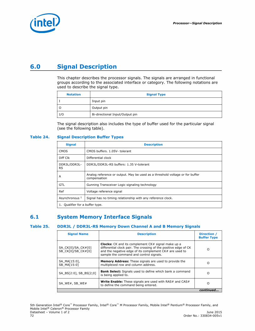
6.0 Signal Description
This chapter describes the processor signals. The signals are arranged in functionalgroups according to the associated interface or category. The following notations areused to describe the signal type.
Notation Signal Type
I Input pin
O Output pin
I/O Bi-directional Input/Output pin
The signal description also includes the type of buffer used for the particular signal(see the following table).
Table 24. Signal Description Buffer Types
Signal Description
CMOS CMOS buffers. 1.05V- tolerant
Diff Clk Differential clock
DDR3L/DDR3L-RS
DDR3L/DDR3L-RS buffers: 1.35 V-tolerant
A Analog reference or output. May be used as a threshold voltage or for buffercompensation
GTL Gunning Transceiver Logic signaling technology
Ref Voltage reference signal
Asynchronous 1 Signal has no timing relationship with any reference clock.
1. Qualifier for a buffer type.
System Memory Interface Signals
Table 25. DDR3L / DDR3L-RS Memory Down Channel A and B Memory Signals
Signal Name Description Direction /Buffer Type
SA_CK[0]/SA_CK#[0]SB_CK[0]/SB_CK#[0]
Clocks: CK and its complement CK# signal make up adifferential clock pair. The crossing of the positive edge of CKand the negative edge of its complement CK# are used tosample the command and control signals.
O
SA_MA[15:0],SB_MA[15:0]
Memory Address: These signals are used to provide themultiplexed row and column address. O
SA_BS[2:0], SB_BS[2;0] Bank Select: Signals used to define which bank a commandis being applied to. O
SA_WE#, SB_WE# Write Enable: These signals are used with RAS# and CAS#to define the command being entered. O
continued...
6.1
Processor—Signal Description
5th Generation Intel® Core™ Processor Family, Intel® Core™ M Processor Family, Mobile Intel® Pentium® Processor Family, andMobile Intel® Celeron® Processor FamilyDatasheet – Volume 1 of 2 June 201572 Order No.: 330834-005v1
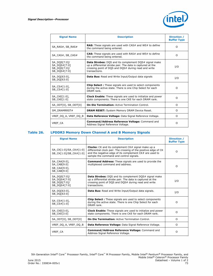
Signal Name Description Direction /Buffer Type
SA_RAS#, SB_RAS# RAS: These signals are used with CAS# and WE# to definethe command being entered. O
SA_CAS#, SB_CAS# CAS: These signals are used with RAS# and WE# to definethe command being entered. O
SA_DQS[7:0]/SA_DQS#[7:0]SB_DQS[7:0]/SB_DQS#[7:0]
Data Strobes: DQS and its complement DQS# signal makeup a differential strobe pair. The data is captured at thecrossing point of DQS and DQS# during read and writetransactions.
I/O
SA_DQ[63:0],SB_DQ[63:0]
Data Bus: Read and Write Input/Output data signals I/O
SA_CS#[1:0],SB_CS#[1:0]
Chip Select : These signals are used to select componentsduring the active state. There is one Chip Select for eachDRAM rank.
O
SA_CKE[1:0],SB_CKE[1:0]
Clock Enable: These signals are used to initialize and powerstate components. There is one CKE for each DRAM rank. O
SA_ODT[0], SB_ODT[0] On Die Termination: Active Termination Control. O
SM_DRAMRRST# DRAM RESET: System Memory DRAM Device Reset. O
VREF_DQ_A, VREF_DQ_B Data Reference Voltage: Data Signal Reference Voltage. O
VREF_CA Command/Address Reference Voltage: Command andAddress Signal Reference Voltage. O
Table 26. LPDDR3 Memory Down Channel A and B Memory Signals
Signal Name Description Direction /Buffer Type
SA_CK[1:0]/SA_CK#[1:0]SB_CK[1:0]/SB_CK#[1:0]
Clocks: CK and its complement CK# signal make up adifferential clock pair. The crossing of the positive edge of CKand the negative edge of its complement CK# are used tosample the command and control signals.
O
SA_CAA[9:0],SA_CAB[9:0]SB_CAA[9:0],SB_CAB[9:0]
Command Address: These signals are used to provide themultiplexed command and address.
O
SA_DQS[7:0]/SA_DQS#[7:0]SB_DQS[7:0]/SB_DQS#[7:0]
Data Strobes: DQS and its complement DQS# signal makeup a differential strobe pair. The data is captured at thecrossing point of DQS and DQS# during read and writetransactions.
I/O
SA_DQ[63:0],SB_DQ[63:0]
Data Bus: Read and Write Input/Output data signals. I/O
SA_CS#[1:0],SB_CS#[1:0]
Chip Select : These signals are used to select componentsduring the active state. There is one Chip Select for eachDRAM rank.
O
SA_CKE[3:0],SB_CKE[3:0]
Clock Enable: These signals are used to initialize and powerstate components. There is one CKE for each DRAM rank. O
SA_ODT[0], SB_ODT[0] On Die Termination: Active Termination Control. O
VREF_DQ_A, VREF_DQ_B Data Reference Voltage: Data Signal Reference Voltage. O
VREF_CA Command/Address Reference Voltage: Command andAddress Signal Reference Voltage. O
Signal Description—Processor
5th Generation Intel® Core™ Processor Family, Intel® Core™ M Processor Family, Mobile Intel® Pentium® Processor Family, andMobile Intel® Celeron® Processor Family
June 2015 Datasheet – Volume 1 of 2Order No.: 330834-005v1 73
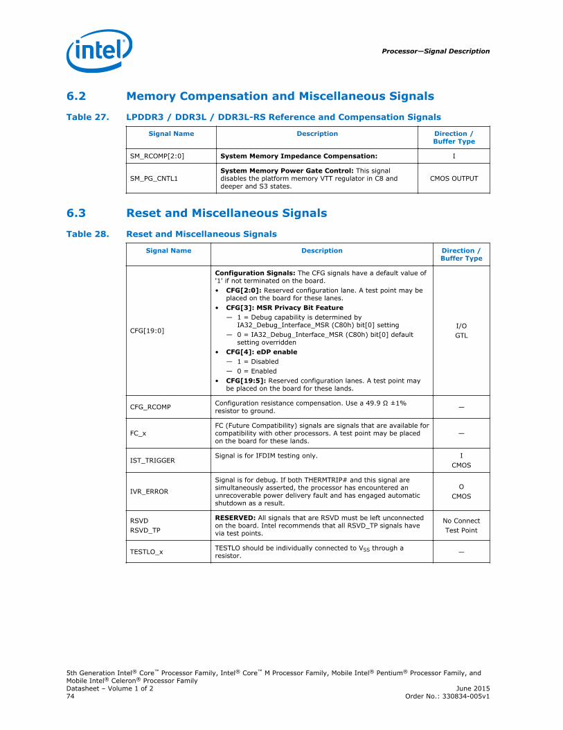
Memory Compensation and Miscellaneous Signals
Table 27. LPDDR3 / DDR3L / DDR3L-RS Reference and Compensation Signals
Signal Name Description Direction /Buffer Type
SM_RCOMP[2:0] System Memory Impedance Compensation: I
SM_PG_CNTL1System Memory Power Gate Control: This signaldisables the platform memory VTT regulator in C8 anddeeper and S3 states.
CMOS OUTPUT
Reset and Miscellaneous Signals
Table 28. Reset and Miscellaneous Signals
Signal Name Description Direction /Buffer Type
CFG[19:0]
Configuration Signals: The CFG signals have a default value of'1' if not terminated on the board.• CFG[2:0]: Reserved configuration lane. A test point may be
placed on the board for these lanes.• CFG[3]: MSR Privacy Bit Feature
— 1 = Debug capability is determined byIA32_Debug_Interface_MSR (C80h) bit[0] setting
— 0 = IA32_Debug_Interface_MSR (C80h) bit[0] defaultsetting overridden
• CFG[4]: eDP enable— 1 = Disabled— 0 = Enabled
• CFG[19:5]: Reserved configuration lanes. A test point maybe placed on the board for these lands.
I/OGTL
CFG_RCOMP Configuration resistance compensation. Use a 49.9 Ω ±1%resistor to ground. —
FC_xFC (Future Compatibility) signals are signals that are available forcompatibility with other processors. A test point may be placedon the board for these lands.
—
IST_TRIGGERSignal is for IFDIM testing only. I
CMOS
IVR_ERROR
Signal is for debug. If both THERMTRIP# and this signal aresimultaneously asserted, the processor has encountered anunrecoverable power delivery fault and has engaged automaticshutdown as a result.
OCMOS
RSVDRSVD_TP
RESERVED: All signals that are RSVD must be left unconnectedon the board. Intel recommends that all RSVD_TP signals havevia test points.
No ConnectTest Point
TESTLO_x TESTLO should be individually connected to VSS through aresistor. —
6.2
6.3
Processor—Signal Description
5th Generation Intel® Core™ Processor Family, Intel® Core™ M Processor Family, Mobile Intel® Pentium® Processor Family, andMobile Intel® Celeron® Processor FamilyDatasheet – Volume 1 of 2 June 201574 Order No.: 330834-005v1
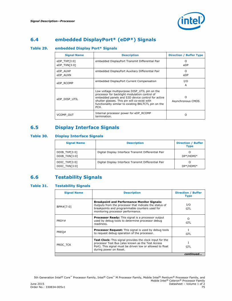
embedded DisplayPort* (eDP*) Signals
Table 29. embedded Display Port* Signals
Signal Name Description Direction / Buffer Type
eDP_TXP[3:0]eDP_TXN[3:0]
embedded DisplayPort Transmit Differential Pair OeDP
eDP_AUXPeDP_AUXN
embedded DisplayPort Auxiliary Differential Pair OeDP
eDP_RCOMPembedded DisplayPort Current Compensation I/O
A
eDP_DISP_UTIL
Low voltage multipurpose DISP_UTIL pin on theprocessor for backlight modulation control ofembedded panels and S3D device control for activeshutter glasses. This pin will co-exist withfunctionality similar to existing BKLTCTL pin on thePCH.
OAsynchronous CMOS
VCOMP_OUT Internal processor power for eDP_RCOMPtermination. O
Display Interface Signals
Table 30. Display Interface Signals
Signal Name Description Direction / BufferType
DDIB_TXP[3:0]DDIB_TXN[3:0]
Digital Display Interface Transmit Differential Pair ODP*/HDMI*
DDIC_TXP[3:0]DDIC_TXN[3:0]
Digital Display Interface Transmit Differential Pair ODP*/HDMI*
Testability Signals
Table 31. Testability Signals
Signal Name Description Direction / BufferType
BPM#[7:0]
Breakpoint and Performance Monitor Signals:Outputs from the processor that indicate the status ofbreakpoints and programmable counters used formonitoring processor performance.
I/OGTL
PRDY#Processor Ready: This signal is a processor outputused by debug tools to determine processor debugreadiness.
OGTL
PREQ#Processor Request: This signal is used by debug toolsto request debug operation of the processor.
IGTL
PROC_TCK
Test Clock: This signal provides the clock input for theprocessor Test Bus (also known as the Test AccessPort). This signal must be driven low or allowed to floatduring power on Reset.
IGTL
continued...
6.4
6.5
6.6
Signal Description—Processor
5th Generation Intel® Core™ Processor Family, Intel® Core™ M Processor Family, Mobile Intel® Pentium® Processor Family, andMobile Intel® Celeron® Processor Family
June 2015 Datasheet – Volume 1 of 2Order No.: 330834-005v1 75
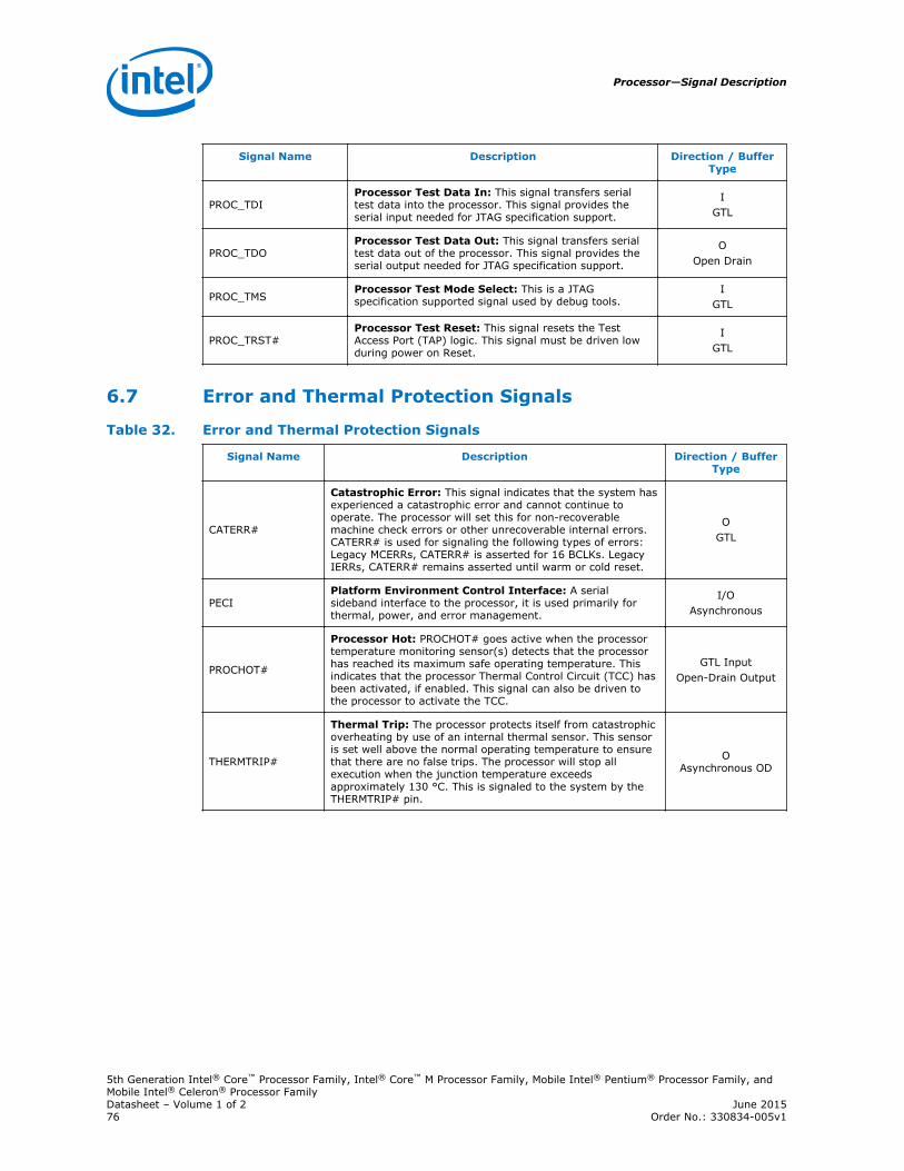
Signal Name Description Direction / BufferType
PROC_TDIProcessor Test Data In: This signal transfers serialtest data into the processor. This signal provides theserial input needed for JTAG specification support.
IGTL
PROC_TDOProcessor Test Data Out: This signal transfers serialtest data out of the processor. This signal provides theserial output needed for JTAG specification support.
OOpen Drain
PROC_TMSProcessor Test Mode Select: This is a JTAGspecification supported signal used by debug tools.
IGTL
PROC_TRST#Processor Test Reset: This signal resets the TestAccess Port (TAP) logic. This signal must be driven lowduring power on Reset.
IGTL
Error and Thermal Protection Signals
Table 32. Error and Thermal Protection Signals
Signal Name Description Direction / BufferType
CATERR#
Catastrophic Error: This signal indicates that the system hasexperienced a catastrophic error and cannot continue tooperate. The processor will set this for non-recoverablemachine check errors or other unrecoverable internal errors.CATERR# is used for signaling the following types of errors:Legacy MCERRs, CATERR# is asserted for 16 BCLKs. LegacyIERRs, CATERR# remains asserted until warm or cold reset.
OGTL
PECIPlatform Environment Control Interface: A serialsideband interface to the processor, it is used primarily forthermal, power, and error management.
I/OAsynchronous
PROCHOT#
Processor Hot: PROCHOT# goes active when the processortemperature monitoring sensor(s) detects that the processorhas reached its maximum safe operating temperature. Thisindicates that the processor Thermal Control Circuit (TCC) hasbeen activated, if enabled. This signal can also be driven tothe processor to activate the TCC.
GTL InputOpen-Drain Output
THERMTRIP#
Thermal Trip: The processor protects itself from catastrophicoverheating by use of an internal thermal sensor. This sensoris set well above the normal operating temperature to ensurethat there are no false trips. The processor will stop allexecution when the junction temperature exceedsapproximately 130 °C. This is signaled to the system by theTHERMTRIP# pin.
OAsynchronous OD
6.7
Processor—Signal Description
5th Generation Intel® Core™ Processor Family, Intel® Core™ M Processor Family, Mobile Intel® Pentium® Processor Family, andMobile Intel® Celeron® Processor FamilyDatasheet – Volume 1 of 2 June 201576 Order No.: 330834-005v1
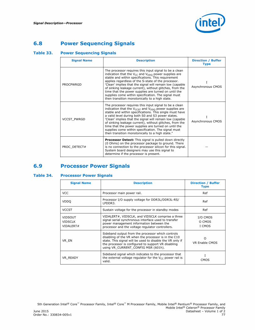
Power Sequencing Signals
Table 33. Power Sequencing Signals
Signal Name Description Direction / BufferType
PROCPWRGD
The processor requires this input signal to be a cleanindication that the VCC and VDDQ power supplies arestable and within specifications. This requirementapplies regardless of the S-state of the processor.'Clean' implies that the signal will remain low (capableof sinking leakage current), without glitches, from thetime that the power supplies are turned on until thesupplies come within specification. The signal mustthen transition monotonically to a high state.
IAsynchronous CMOS
VCCST_PWRGD
The processor requires this input signal to be a cleanindication that the VCCST and VDDQ power supplies arestable and within specifications. This single must havea valid level during both S0 and S3 power states.'Clean' implies that the signal will remain low (capableof sinking leakage current), without glitches, from thetime that the power supplies are turned on until thesupplies come within specification. The signal mustthen transition monotonically to a high state."
IAsynchronous CMOS
PROC_DETECT#
Processor Detect: This signal is pulled down directly(0 Ohms) on the processor package to ground. Thereis no connection to the processor silicon for this signal.System board designers may use this signal todetermine if the processor is present.
—
Processor Power Signals
Table 34. Processor Power Signals
Signal Name Description Direction / BufferType
VCC Processor main power rail. Ref
VDDQ Processor I/O supply voltage for DDR3L/DDR3L-RS/LPDDR3. Ref
VCCST Sustain voltage for the processor in standby modes Ref
VIDSOUTVIDSCLKVIDALERT#
VIDALERT#, VIDSCLK, and VIDSCLK comprise a threesignal serial synchronous interface used to transferpower management information between theprocessor and the voltage regulator controllers.
I/O CMOSO CMOSI CMOS
VR_EN
Sideband output from the processor which controlsdisabling of the VR when the processor is in the C10state. This signal will be used to disable the VR only ifthe processor is configured to support VR disablingusing VR_CURRENT_CONFIG MSR (601h).
OVR Enable CMOS
VR_READYSideband signal which indicates to the processor thatthe external voltage regulator for the VCC power rail isvalid.
ICMOS
6.8
6.9
Signal Description—Processor
5th Generation Intel® Core™ Processor Family, Intel® Core™ M Processor Family, Mobile Intel® Pentium® Processor Family, andMobile Intel® Celeron® Processor Family
June 2015 Datasheet – Volume 1 of 2Order No.: 330834-005v1 77
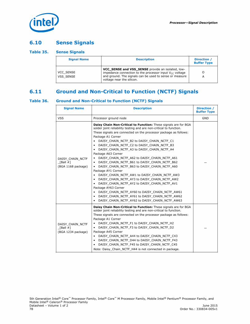
Sense Signals
Table 35. Sense Signals
Signal Name Description Direction /Buffer Type
VCC_SENSEVSS_SENSE
VCC_SENSE and VSS_SENSE provide an isolated, low-impedance connection to the processor input VCC voltageand ground. The signals can be used to sense or measurevoltage near the silicon.
OA
Ground and Non-Critical to Function (NCTF) Signals
Table 36. Ground and Non-Critical to Function (NCTF) Signals
Signal Name Description Direction /Buffer Type
VSS Processor ground node GND
DAISY_CHAIN_NCTF_[Ball #](BGA 1168 package)
Daisy Chain Non-Critical to Function: These signals are for BGAsolder joint reliability testing and are non-critical to function.These signals are connected on the processor package as follows:Package A1 Corner• DAISY_CHAIN_NCTF_B2 to DAISY_CHAIN_NCTF_C1• DAISY_CHAIN_NCTF_C2 to DAISY_CHAIN_NCTF_B3• DAISY_CHAIN_NCTF_A3 to DAISY_CHAIN_NCTF_A4Package A63 Corner• DAISY_CHAIN_NCTF_A62 to DAISY_CHAIN_NCTF_A61• DAISY_CHAIN_NCTF_B61 to DAISY_CHAIN_NCTF_B62• DAISY_CHAIN_NCTF_B63 to DAISY_CHAIN_NCTF_A60Package AY1 Corner• DAISY_CHAIN_NCTF_AW1 to DAISY_CHAIN_NCTF_AW3• DAISY_CHAIN_NCTF_AY3 to DAISY_CHAIN_NCTF_AW2• DAISY_CHAIN_NCTF_AY2 to DAISY_CHAIN_NCTF_AV1Package AY63 Corner• DAISY_CHAIN_NCTF_AY60 to DAISY_CHAIN_NCTF_AW61• DAISY_CHAIN_NCTF_AY61 to DAISY_CHAIN_NCTF_AW62• DAISY_CHAIN_NCTF_AY62 to DAISY_CHAIN_NCTF_AW63
—
DAISY_CHAIN_NCTF_[Ball #](BGA 1234 package)
Daisy Chain Non-Critical to Function: These signals are for BGAsolder joint reliability testing and are non-critical to function.These signals are connected on the processor package as follows:Package A1 Corner• DAISY_CHAIN_NCTF_F1 to DAISY_CHAIN_NCTF_H2• DAISY_CHAIN_NCTF_F3 to DAISY_CHAIN_NCTF_D2Package A45 Corner• DAISY_CHAIN_NCTF_A44 to DAISY_CHAIN_NCTF_C43• DAISY_CHAIN_NCTF_D44 to DAISY_CHAIN_NCTF_F43• DAISY_CHAIN_NCTF_F45 to DAISY_CHAIN_NCTF_C45Note: Daisy_Chain_NCTF_H44 is not connected in package.
—
6.10
6.11
Processor—Signal Description
5th Generation Intel® Core™ Processor Family, Intel® Core™ M Processor Family, Mobile Intel® Pentium® Processor Family, andMobile Intel® Celeron® Processor FamilyDatasheet – Volume 1 of 2 June 201578 Order No.: 330834-005v1
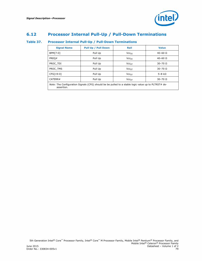
Processor Internal Pull-Up / Pull-Down Terminations
Table 37. Processor Internal Pull-Up / Pull-Down Terminations
Signal Name Pull Up / Pull Down Rail Value
BPM[7:0] Pull Up VccIO 40–60 Ω
PREQ# Pull Up VccIO 40–60 Ω
PROC_TDI Pull Up VccST 30–70 Ω
PROC_TMS Pull Up VccST 30–70 Ω
CFG[19:0] Pull Up VccST 5–8 kΩ
CATERR# Pull Up VccST 30–70 Ω
Note: The Configuration Signals (CFG) should be be pulled to a stable logic value up to PLTRST# de-assertion.
6.12
Signal Description—Processor
5th Generation Intel® Core™ Processor Family, Intel® Core™ M Processor Family, Mobile Intel® Pentium® Processor Family, andMobile Intel® Celeron® Processor Family
June 2015 Datasheet – Volume 1 of 2Order No.: 330834-005v1 79
7.0 Electrical Specifications
This chapter provides the processor electrical specifications including integratedvoltage regulator (VR), VCC Voltage Identification (VID), reserved and unused signals,signal groups, Test Access Points (TAP), and DC specifications.
Integrated Voltage Regulator
A feature to the processor is the integration of platform voltage regulators into theprocessor. Due to this integration, the processor has one main voltage rail (VCC) and avoltage rail for the memory interface (VDDQ) , compared to six voltage rails onprevious processors. The VCC voltage rail will supply the integrated voltage regulatorswhich in turn will regulate to the appropriate voltages for the cores, cache, systemagent, and graphics. This integration allows the processor to better control on-dievoltages to optimize between performance and power savings. The processor VCC railwill remain a VID-based voltage with a loadline similar to the core voltage rail (alsocalled VCC) in previous processors.
Power and Ground Pins
The processor has VCC, VDDQ, and VSS (ground) pins for on-chip power distribution.All power pins must be connected to their respective processor power planes; all VSSpins must be connected to the system ground plane. Use of multiple power andground planes is recommended to reduce I*R drop. The VCC pins must be suppliedwith the voltage determined by the processor Serial Voltage IDentification (SVID)interface. Table 38 on page 81 specifies the voltage level for the various VIDs.
VCC Voltage Identification (VID)
The processor uses three signals for the serial voltage identification interface tosupport automatic selection of voltages. The following table specifies the voltage levelcorresponding to the 8-bit VID value transmitted over serial VID. A ‘1’ in this tablerefers to a high voltage level and a ‘0’ refers to a low voltage level. If the voltageregulation circuit cannot supply the voltage that is requested, the voltage regulatormust disable itself. VID signals are CMOS push/pull drivers. See the Voltage andCurrent Specifications section for the DC specifications for these signals. The VIDcodes will change due to temperature and/or current load changes to minimize thepower of the part. A voltage range is provided in the Voltage and CurrentSpecifications section. The specifications are set so that one voltage regulator canoperate with all supported frequencies.
Individual processor VID values may be set during manufacturing so that two devicesat the same core frequency may have different default VID settings. This is shown inthe VID range values in the Voltage and Current Specifications section. The processorprovides the ability to operate while transitioning to an adjacent VID and itsassociated voltage. This will represent a DC shift in the loadline.
7.1
7.2
7.3
Processor—Electrical Specifications
5th Generation Intel® Core™ Processor Family, Intel® Core™ M Processor Family, Mobile Intel® Pentium® Processor Family, andMobile Intel® Celeron® Processor FamilyDatasheet – Volume 1 of 2 June 201580 Order No.: 330834-005v1
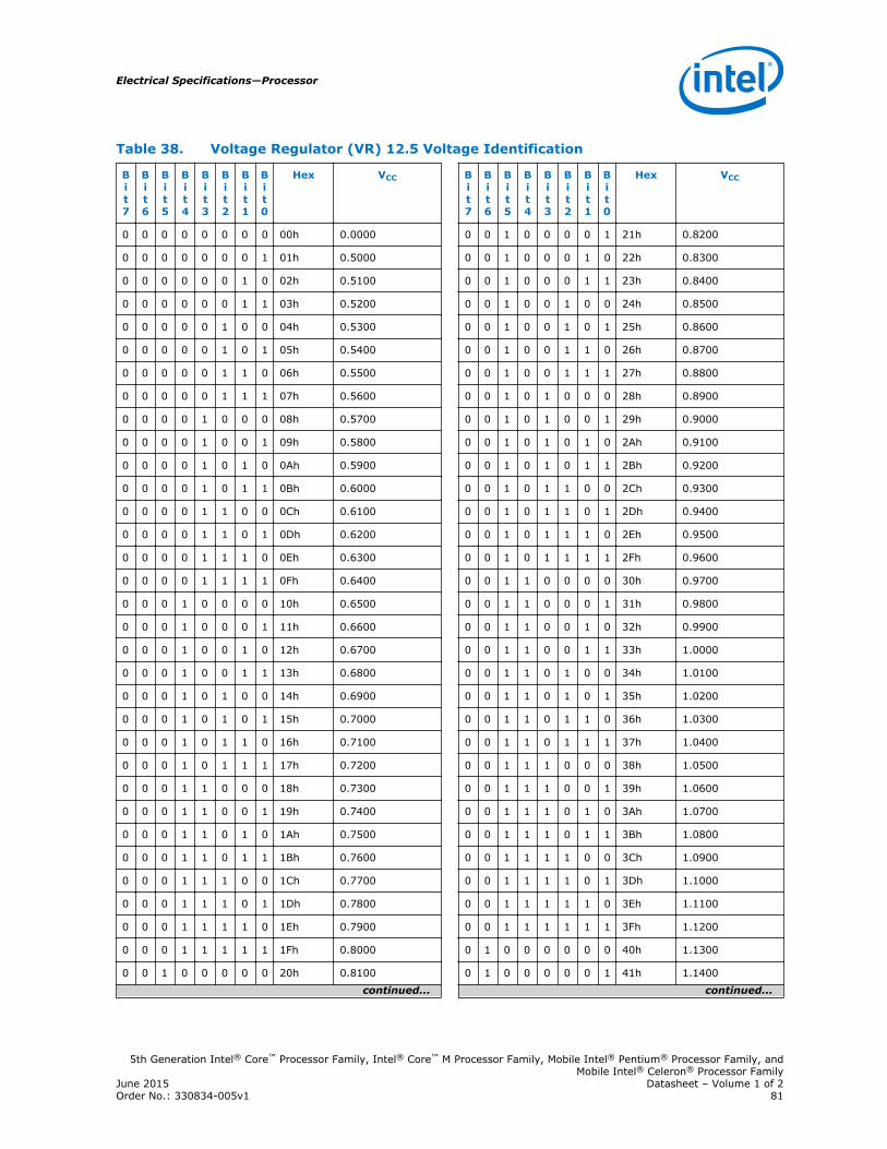
Table 38. Voltage Regulator (VR) 12.5 Voltage Identification
Bit7
Bit6
Bit5
Bit4
Bit3
Bit2
Bit1
Bit0
Hex VCC
0 0 0 0 0 0 0 0 00h 0.0000
0 0 0 0 0 0 0 1 01h 0.5000
0 0 0 0 0 0 1 0 02h 0.5100
0 0 0 0 0 0 1 1 03h 0.5200
0 0 0 0 0 1 0 0 04h 0.5300
0 0 0 0 0 1 0 1 05h 0.5400
0 0 0 0 0 1 1 0 06h 0.5500
0 0 0 0 0 1 1 1 07h 0.5600
0 0 0 0 1 0 0 0 08h 0.5700
0 0 0 0 1 0 0 1 09h 0.5800
0 0 0 0 1 0 1 0 0Ah 0.5900
0 0 0 0 1 0 1 1 0Bh 0.6000
0 0 0 0 1 1 0 0 0Ch 0.6100
0 0 0 0 1 1 0 1 0Dh 0.6200
0 0 0 0 1 1 1 0 0Eh 0.6300
0 0 0 0 1 1 1 1 0Fh 0.6400
0 0 0 1 0 0 0 0 10h 0.6500
0 0 0 1 0 0 0 1 11h 0.6600
0 0 0 1 0 0 1 0 12h 0.6700
0 0 0 1 0 0 1 1 13h 0.6800
0 0 0 1 0 1 0 0 14h 0.6900
0 0 0 1 0 1 0 1 15h 0.7000
0 0 0 1 0 1 1 0 16h 0.7100
0 0 0 1 0 1 1 1 17h 0.7200
0 0 0 1 1 0 0 0 18h 0.7300
0 0 0 1 1 0 0 1 19h 0.7400
0 0 0 1 1 0 1 0 1Ah 0.7500
0 0 0 1 1 0 1 1 1Bh 0.7600
0 0 0 1 1 1 0 0 1Ch 0.7700
0 0 0 1 1 1 0 1 1Dh 0.7800
0 0 0 1 1 1 1 0 1Eh 0.7900
0 0 0 1 1 1 1 1 1Fh 0.8000
0 0 1 0 0 0 0 0 20h 0.8100
continued...
Bit7
Bit6
Bit5
Bit4
Bit3
Bit2
Bit1
Bit0
Hex VCC
0 0 1 0 0 0 0 1 21h 0.8200
0 0 1 0 0 0 1 0 22h 0.8300
0 0 1 0 0 0 1 1 23h 0.8400
0 0 1 0 0 1 0 0 24h 0.8500
0 0 1 0 0 1 0 1 25h 0.8600
0 0 1 0 0 1 1 0 26h 0.8700
0 0 1 0 0 1 1 1 27h 0.8800
0 0 1 0 1 0 0 0 28h 0.8900
0 0 1 0 1 0 0 1 29h 0.9000
0 0 1 0 1 0 1 0 2Ah 0.9100
0 0 1 0 1 0 1 1 2Bh 0.9200
0 0 1 0 1 1 0 0 2Ch 0.9300
0 0 1 0 1 1 0 1 2Dh 0.9400
0 0 1 0 1 1 1 0 2Eh 0.9500
0 0 1 0 1 1 1 1 2Fh 0.9600
0 0 1 1 0 0 0 0 30h 0.9700
0 0 1 1 0 0 0 1 31h 0.9800
0 0 1 1 0 0 1 0 32h 0.9900
0 0 1 1 0 0 1 1 33h 1.0000
0 0 1 1 0 1 0 0 34h 1.0100
0 0 1 1 0 1 0 1 35h 1.0200
0 0 1 1 0 1 1 0 36h 1.0300
0 0 1 1 0 1 1 1 37h 1.0400
0 0 1 1 1 0 0 0 38h 1.0500
0 0 1 1 1 0 0 1 39h 1.0600
0 0 1 1 1 0 1 0 3Ah 1.0700
0 0 1 1 1 0 1 1 3Bh 1.0800
0 0 1 1 1 1 0 0 3Ch 1.0900
0 0 1 1 1 1 0 1 3Dh 1.1000
0 0 1 1 1 1 1 0 3Eh 1.1100
0 0 1 1 1 1 1 1 3Fh 1.1200
0 1 0 0 0 0 0 0 40h 1.1300
0 1 0 0 0 0 0 1 41h 1.1400
continued...
Electrical Specifications—Processor
5th Generation Intel® Core™ Processor Family, Intel® Core™ M Processor Family, Mobile Intel® Pentium® Processor Family, andMobile Intel® Celeron® Processor Family
June 2015 Datasheet – Volume 1 of 2Order No.: 330834-005v1 81
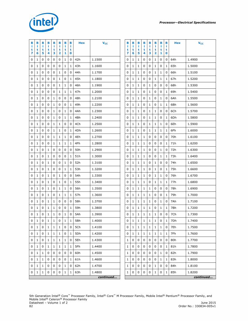
Bit7
Bit6
Bit5
Bit4
Bit3
Bit2
Bit1
Bit0
Hex VCC
0 1 0 0 0 0 1 0 42h 1.1500
0 1 0 0 0 0 1 1 43h 1.1600
0 1 0 0 0 1 0 0 44h 1.1700
0 1 0 0 0 1 0 1 45h 1.1800
0 1 0 0 0 1 1 0 46h 1.1900
0 1 0 0 0 1 1 1 47h 1.2000
0 1 0 0 1 0 0 0 48h 1.2100
0 1 0 0 1 0 0 1 49h 1.2200
0 1 0 0 1 0 1 0 4Ah 1.2300
0 1 0 0 1 0 1 1 4Bh 1.2400
0 1 0 0 1 1 0 0 4Ch 1.2500
0 1 0 0 1 1 0 1 4Dh 1.2600
0 1 0 0 1 1 1 0 4Eh 1.2700
0 1 0 0 1 1 1 1 4Fh 1.2800
0 1 0 1 0 0 0 0 50h 1.2900
0 1 0 1 0 0 0 1 51h 1.3000
0 1 0 1 0 0 1 0 52h 1.3100
0 1 0 1 0 0 1 1 53h 1.3200
0 1 0 1 0 1 0 0 54h 1.3300
0 1 0 1 0 1 0 1 55h 1.3400
0 1 0 1 0 1 1 0 56h 1.3500
0 1 0 1 0 1 1 1 57h 1.3600
0 1 0 1 1 0 0 0 58h 1.3700
0 1 0 1 1 0 0 1 59h 1.3800
0 1 0 1 1 0 1 0 5Ah 1.3900
0 1 0 1 1 0 1 1 5Bh 1.4000
0 1 0 1 1 1 0 0 5Ch 1.4100
0 1 0 1 1 1 0 1 5Dh 1.4200
0 1 0 1 1 1 1 0 5Eh 1.4300
0 1 0 1 1 1 1 1 5Fh 1.4400
0 1 1 0 0 0 0 0 60h 1.4500
0 1 1 0 0 0 0 1 61h 1.4600
0 1 1 0 0 0 1 0 62h 1.4700
0 1 1 0 0 0 1 1 63h 1.4800
continued...
Bit7
Bit6
Bit5
Bit4
Bit3
Bit2
Bit1
Bit0
Hex VCC
0 1 1 0 0 1 0 0 64h 1.4900
0 1 1 0 0 1 0 1 65h 1.5000
0 1 1 0 0 1 1 0 66h 1.5100
0 1 1 0 0 1 1 1 67h 1.5200
0 1 1 0 1 0 0 0 68h 1.5300
0 1 1 0 1 0 0 1 69h 1.5400
0 1 1 0 1 0 1 0 6Ah 1.5500
0 1 1 0 1 0 1 1 6Bh 1.5600
0 1 1 0 1 1 0 0 6Ch 1.5700
0 1 1 0 1 1 0 1 6Dh 1.5800
0 1 1 0 1 1 1 0 6Eh 1.5900
0 1 1 0 1 1 1 1 6Fh 1.6000
0 1 1 1 0 0 0 0 70h 1.6100
0 1 1 1 0 0 0 1 71h 1.6200
0 1 1 1 0 0 1 0 72h 1.6300
0 1 1 1 0 0 1 1 73h 1.6400
0 1 1 1 0 1 0 0 74h 1.6500
0 1 1 1 0 1 0 1 75h 1.6600
0 1 1 1 0 1 1 0 76h 1.6700
0 1 1 1 0 1 1 1 77h 1.6800
0 1 1 1 1 0 0 0 78h 1.6900
0 1 1 1 1 0 0 1 79h 1.7000
0 1 1 1 1 0 1 0 7Ah 1.7100
0 1 1 1 1 0 1 1 7Bh 1.7200
0 1 1 1 1 1 0 0 7Ch 1.7300
0 1 1 1 1 1 0 1 7Dh 1.7400
0 1 1 1 1 1 1 0 7Eh 1.7500
0 1 1 1 1 1 1 1 7Fh 1.7600
1 0 0 0 0 0 0 0 80h 1.7700
1 0 0 0 0 0 0 1 81h 1.7800
1 0 0 0 0 0 1 0 82h 1.7900
1 0 0 0 0 0 1 1 83h 1.8000
1 0 0 0 0 1 0 0 84h 1.8100
1 0 0 0 0 1 0 1 85h 1.8200
continued...
Processor—Electrical Specifications
5th Generation Intel® Core™ Processor Family, Intel® Core™ M Processor Family, Mobile Intel® Pentium® Processor Family, andMobile Intel® Celeron® Processor FamilyDatasheet – Volume 1 of 2 June 201582 Order No.: 330834-005v1
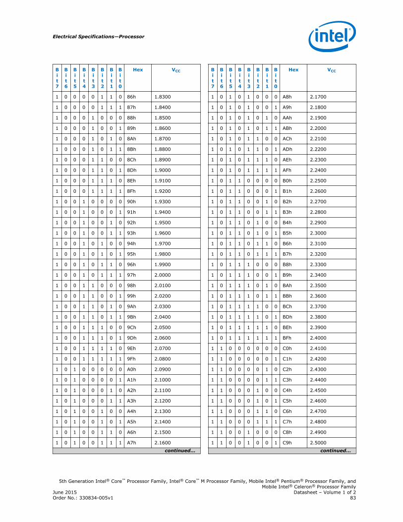
Bit7
Bit6
Bit5
Bit4
Bit3
Bit2
Bit1
Bit0
Hex VCC
1 0 0 0 0 1 1 0 86h 1.8300
1 0 0 0 0 1 1 1 87h 1.8400
1 0 0 0 1 0 0 0 88h 1.8500
1 0 0 0 1 0 0 1 89h 1.8600
1 0 0 0 1 0 1 0 8Ah 1.8700
1 0 0 0 1 0 1 1 8Bh 1.8800
1 0 0 0 1 1 0 0 8Ch 1.8900
1 0 0 0 1 1 0 1 8Dh 1.9000
1 0 0 0 1 1 1 0 8Eh 1.9100
1 0 0 0 1 1 1 1 8Fh 1.9200
1 0 0 1 0 0 0 0 90h 1.9300
1 0 0 1 0 0 0 1 91h 1.9400
1 0 0 1 0 0 1 0 92h 1.9500
1 0 0 1 0 0 1 1 93h 1.9600
1 0 0 1 0 1 0 0 94h 1.9700
1 0 0 1 0 1 0 1 95h 1.9800
1 0 0 1 0 1 1 0 96h 1.9900
1 0 0 1 0 1 1 1 97h 2.0000
1 0 0 1 1 0 0 0 98h 2.0100
1 0 0 1 1 0 0 1 99h 2.0200
1 0 0 1 1 0 1 0 9Ah 2.0300
1 0 0 1 1 0 1 1 9Bh 2.0400
1 0 0 1 1 1 0 0 9Ch 2.0500
1 0 0 1 1 1 0 1 9Dh 2.0600
1 0 0 1 1 1 1 0 9Eh 2.0700
1 0 0 1 1 1 1 1 9Fh 2.0800
1 0 1 0 0 0 0 0 A0h 2.0900
1 0 1 0 0 0 0 1 A1h 2.1000
1 0 1 0 0 0 1 0 A2h 2.1100
1 0 1 0 0 0 1 1 A3h 2.1200
1 0 1 0 0 1 0 0 A4h 2.1300
1 0 1 0 0 1 0 1 A5h 2.1400
1 0 1 0 0 1 1 0 A6h 2.1500
1 0 1 0 0 1 1 1 A7h 2.1600
continued...
Bit7
Bit6
Bit5
Bit4
Bit3
Bit2
Bit1
Bit0
Hex VCC
1 0 1 0 1 0 0 0 A8h 2.1700
1 0 1 0 1 0 0 1 A9h 2.1800
1 0 1 0 1 0 1 0 AAh 2.1900
1 0 1 0 1 0 1 1 ABh 2.2000
1 0 1 0 1 1 0 0 ACh 2.2100
1 0 1 0 1 1 0 1 ADh 2.2200
1 0 1 0 1 1 1 0 AEh 2.2300
1 0 1 0 1 1 1 1 AFh 2.2400
1 0 1 1 0 0 0 0 B0h 2.2500
1 0 1 1 0 0 0 1 B1h 2.2600
1 0 1 1 0 0 1 0 B2h 2.2700
1 0 1 1 0 0 1 1 B3h 2.2800
1 0 1 1 0 1 0 0 B4h 2.2900
1 0 1 1 0 1 0 1 B5h 2.3000
1 0 1 1 0 1 1 0 B6h 2.3100
1 0 1 1 0 1 1 1 B7h 2.3200
1 0 1 1 1 0 0 0 B8h 2.3300
1 0 1 1 1 0 0 1 B9h 2.3400
1 0 1 1 1 0 1 0 BAh 2.3500
1 0 1 1 1 0 1 1 BBh 2.3600
1 0 1 1 1 1 0 0 BCh 2.3700
1 0 1 1 1 1 0 1 BDh 2.3800
1 0 1 1 1 1 1 0 BEh 2.3900
1 0 1 1 1 1 1 1 BFh 2.4000
1 1 0 0 0 0 0 0 C0h 2.4100
1 1 0 0 0 0 0 1 C1h 2.4200
1 1 0 0 0 0 1 0 C2h 2.4300
1 1 0 0 0 0 1 1 C3h 2.4400
1 1 0 0 0 1 0 0 C4h 2.4500
1 1 0 0 0 1 0 1 C5h 2.4600
1 1 0 0 0 1 1 0 C6h 2.4700
1 1 0 0 0 1 1 1 C7h 2.4800
1 1 0 0 1 0 0 0 C8h 2.4900
1 1 0 0 1 0 0 1 C9h 2.5000
continued...
Electrical Specifications—Processor
5th Generation Intel® Core™ Processor Family, Intel® Core™ M Processor Family, Mobile Intel® Pentium® Processor Family, andMobile Intel® Celeron® Processor Family
June 2015 Datasheet – Volume 1 of 2Order No.: 330834-005v1 83
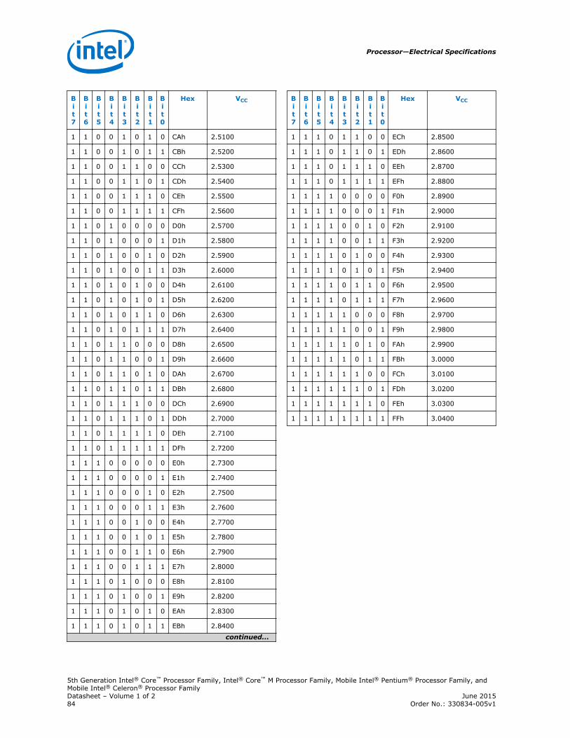
Bit7
Bit6
Bit5
Bit4
Bit3
Bit2
Bit1
Bit0
Hex VCC
1 1 0 0 1 0 1 0 CAh 2.5100
1 1 0 0 1 0 1 1 CBh 2.5200
1 1 0 0 1 1 0 0 CCh 2.5300
1 1 0 0 1 1 0 1 CDh 2.5400
1 1 0 0 1 1 1 0 CEh 2.5500
1 1 0 0 1 1 1 1 CFh 2.5600
1 1 0 1 0 0 0 0 D0h 2.5700
1 1 0 1 0 0 0 1 D1h 2.5800
1 1 0 1 0 0 1 0 D2h 2.5900
1 1 0 1 0 0 1 1 D3h 2.6000
1 1 0 1 0 1 0 0 D4h 2.6100
1 1 0 1 0 1 0 1 D5h 2.6200
1 1 0 1 0 1 1 0 D6h 2.6300
1 1 0 1 0 1 1 1 D7h 2.6400
1 1 0 1 1 0 0 0 D8h 2.6500
1 1 0 1 1 0 0 1 D9h 2.6600
1 1 0 1 1 0 1 0 DAh 2.6700
1 1 0 1 1 0 1 1 DBh 2.6800
1 1 0 1 1 1 0 0 DCh 2.6900
1 1 0 1 1 1 0 1 DDh 2.7000
1 1 0 1 1 1 1 0 DEh 2.7100
1 1 0 1 1 1 1 1 DFh 2.7200
1 1 1 0 0 0 0 0 E0h 2.7300
1 1 1 0 0 0 0 1 E1h 2.7400
1 1 1 0 0 0 1 0 E2h 2.7500
1 1 1 0 0 0 1 1 E3h 2.7600
1 1 1 0 0 1 0 0 E4h 2.7700
1 1 1 0 0 1 0 1 E5h 2.7800
1 1 1 0 0 1 1 0 E6h 2.7900
1 1 1 0 0 1 1 1 E7h 2.8000
1 1 1 0 1 0 0 0 E8h 2.8100
1 1 1 0 1 0 0 1 E9h 2.8200
1 1 1 0 1 0 1 0 EAh 2.8300
1 1 1 0 1 0 1 1 EBh 2.8400
continued...
Bit7
Bit6
Bit5
Bit4
Bit3
Bit2
Bit1
Bit0
Hex VCC
1 1 1 0 1 1 0 0 ECh 2.8500
1 1 1 0 1 1 0 1 EDh 2.8600
1 1 1 0 1 1 1 0 EEh 2.8700
1 1 1 0 1 1 1 1 EFh 2.8800
1 1 1 1 0 0 0 0 F0h 2.8900
1 1 1 1 0 0 0 1 F1h 2.9000
1 1 1 1 0 0 1 0 F2h 2.9100
1 1 1 1 0 0 1 1 F3h 2.9200
1 1 1 1 0 1 0 0 F4h 2.9300
1 1 1 1 0 1 0 1 F5h 2.9400
1 1 1 1 0 1 1 0 F6h 2.9500
1 1 1 1 0 1 1 1 F7h 2.9600
1 1 1 1 1 0 0 0 F8h 2.9700
1 1 1 1 1 0 0 1 F9h 2.9800
1 1 1 1 1 0 1 0 FAh 2.9900
1 1 1 1 1 0 1 1 FBh 3.0000
1 1 1 1 1 1 0 0 FCh 3.0100
1 1 1 1 1 1 0 1 FDh 3.0200
1 1 1 1 1 1 1 0 FEh 3.0300
1 1 1 1 1 1 1 1 FFh 3.0400
Processor—Electrical Specifications
5th Generation Intel® Core™ Processor Family, Intel® Core™ M Processor Family, Mobile Intel® Pentium® Processor Family, andMobile Intel® Celeron® Processor FamilyDatasheet – Volume 1 of 2 June 201584 Order No.: 330834-005v1

Reserved or Unused Signals
The following are the general types of reserved (RSVD) signals and connectionguidelines:
• RSVD – these signals should not be connected
• RSVD_TP – these signals should be routed to a test point
Arbitrary connection of these signals to VCC, VDDQ, VSS, or to any other signal(including each other) may result in component malfunction or incompatibility withfuture processors. See Signal Description on page 72 for a pin listing of the processorand the location of all reserved signals.
For reliable operation, always connect unused inputs or bi-directional signals to anappropriate signal level. Unused active high inputs should be connected through aresistor to ground (VSS). Unused outputs maybe left unconnected; however, this mayinterfere with some Test Access Port (TAP) functions, complicate debug probing, andprevent boundary scan testing. A resistor must be used when tying bi-directionalsignals to power or ground. When tying any signal to power or ground, a resistor willalso allow for system testability.
Signal Groups
Signals are grouped by buffer type and similar characteristics as listed in the followingtable. The buffer type indicates which signaling technology and specifications apply tothe signals. All the differential signals and selected DDR3L / DDR3L-RS / LPDDR3 andControl Sideband signals have On-Die Termination (ODT) resistors. Some signals donot have ODT and need to be terminated on the board.
Note: All Control Sideband Asynchronous signals are required to be asserted/de-asserted forat least 10 BCLKs with maximum Trise/Tfall of 6 ns in order for the processor torecognize the proper signal state.
Table 39. Signal Groups
Signal Group Type Signals
Reference Clocks 2
Differential DDR3L/DDR3L-RSOutput
SA_CK[3:0], SA_CK#[3:0], SB_CK[3:0], SB_CK#[3:0]
LPDDR3 Output SA_CK[1:0], SA_CK#[1:0], SB_CK[1:0], SB_CK#[1:0]
Command and Address Signals 2
Single ended DDR3L/DDR3L-RSOutput
SA_MA[15:0], SB_MA[15:0], SA_BS[2:0], SB_BS[2;0],SA_WE#, SB_WE#, SA_RAS#, SB_RAS#, SA_CAS#, SB_CAS#
LPDDR3 Output SA_CAA[9:0], SA_CAB[9:0], SB_CAA[9:0], SB_CAB[9:0]
Control Signals 2
Single ended DDR3L/DDR3L-RSOutput
SA_CKE[3:0], SB_CKE[3:0], SA_CS#[3:0], SB_CS#[3:0],SA_ODT[3:0], SB_ODT[3:0]
LPDDR3 Output SA_CKE[3:0], SB_CKE[3:0], SA_CS#[1:0], SB_CS#[1:0],SA_ODT0, SB_ODT0
Data Signals 2
continued...
7.4
7.5
Electrical Specifications—Processor
5th Generation Intel® Core™ Processor Family, Intel® Core™ M Processor Family, Mobile Intel® Pentium® Processor Family, andMobile Intel® Celeron® Processor Family
June 2015 Datasheet – Volume 1 of 2Order No.: 330834-005v1 85
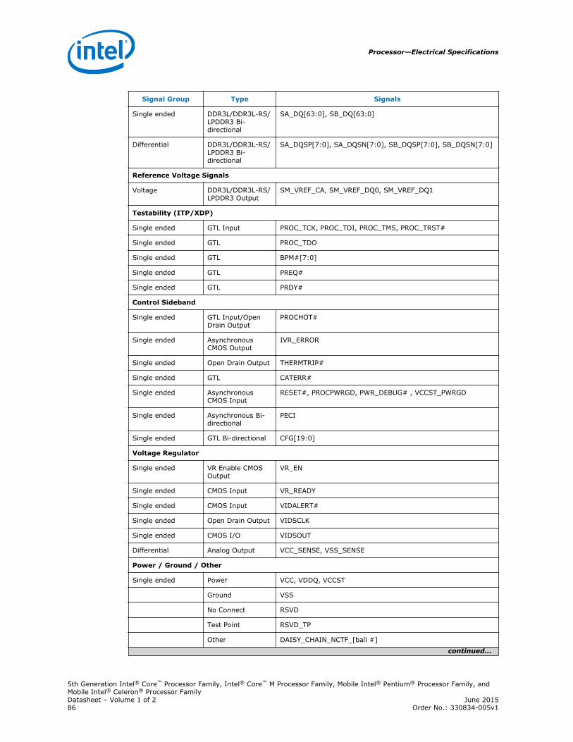
Signal Group Type Signals
Single ended DDR3L/DDR3L-RS/LPDDR3 Bi-directional
SA_DQ[63:0], SB_DQ[63:0]
Differential DDR3L/DDR3L-RS/LPDDR3 Bi-directional
SA_DQSP[7:0], SA_DQSN[7:0], SB_DQSP[7:0], SB_DQSN[7:0]
Reference Voltage Signals
Voltage DDR3L/DDR3L-RS/LPDDR3 Output
SM_VREF_CA, SM_VREF_DQ0, SM_VREF_DQ1
Testability (ITP/XDP)
Single ended GTL Input PROC_TCK, PROC_TDI, PROC_TMS, PROC_TRST#
Single ended GTL PROC_TDO
Single ended GTL BPM#[7:0]
Single ended GTL PREQ#
Single ended GTL PRDY#
Control Sideband
Single ended GTL Input/OpenDrain Output
PROCHOT#
Single ended AsynchronousCMOS Output
IVR_ERROR
Single ended Open Drain Output THERMTRIP#
Single ended GTL CATERR#
Single ended AsynchronousCMOS Input
RESET#, PROCPWRGD, PWR_DEBUG# , VCCST_PWRGD
Single ended Asynchronous Bi-directional
PECI
Single ended GTL Bi-directional CFG[19:0]
Voltage Regulator
Single ended VR Enable CMOSOutput
VR_EN
Single ended CMOS Input VR_READY
Single ended CMOS Input VIDALERT#
Single ended Open Drain Output VIDSCLK
Single ended CMOS I/O VIDSOUT
Differential Analog Output VCC_SENSE, VSS_SENSE
Power / Ground / Other
Single ended Power VCC, VDDQ, VCCST
Ground VSS
No Connect RSVD
Test Point RSVD_TP
Other DAISY_CHAIN_NCTF_[ball #]
continued...
Processor—Electrical Specifications
5th Generation Intel® Core™ Processor Family, Intel® Core™ M Processor Family, Mobile Intel® Pentium® Processor Family, andMobile Intel® Celeron® Processor FamilyDatasheet – Volume 1 of 2 June 201586 Order No.: 330834-005v1
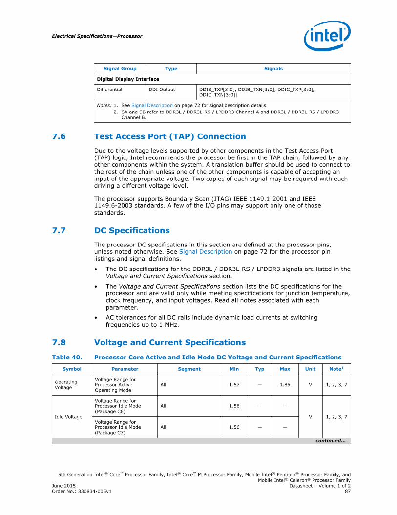
Signal Group Type Signals
Digital Display Interface
Differential DDI Output DDIB_TXP[3:0], DDIB_TXN[3:0], DDIC_TXP[3:0],DDIC_TXN[3:0]]
Notes: 1. See Signal Description on page 72 for signal description details.2. SA and SB refer to DDR3L / DDR3L-RS / LPDDR3 Channel A and DDR3L / DDR3L-RS / LPDDR3
Channel B.
Test Access Port (TAP) Connection
Due to the voltage levels supported by other components in the Test Access Port(TAP) logic, Intel recommends the processor be first in the TAP chain, followed by anyother components within the system. A translation buffer should be used to connect tothe rest of the chain unless one of the other components is capable of accepting aninput of the appropriate voltage. Two copies of each signal may be required with eachdriving a different voltage level.
The processor supports Boundary Scan (JTAG) IEEE 1149.1-2001 and IEEE1149.6-2003 standards. A few of the I/O pins may support only one of thosestandards.
DC Specifications
The processor DC specifications in this section are defined at the processor pins,unless noted otherwise. See Signal Description on page 72 for the processor pinlistings and signal definitions.
• The DC specifications for the DDR3L / DDR3L-RS / LPDDR3 signals are listed in theVoltage and Current Specifications section.
• The Voltage and Current Specifications section lists the DC specifications for theprocessor and are valid only while meeting specifications for junction temperature,clock frequency, and input voltages. Read all notes associated with eachparameter.
• AC tolerances for all DC rails include dynamic load currents at switchingfrequencies up to 1 MHz.
Voltage and Current Specifications
Table 40. Processor Core Active and Idle Mode DC Voltage and Current Specifications
Symbol Parameter Segment Min Typ Max Unit Note1
OperatingVoltage
Voltage Range forProcessor ActiveOperating Mode
All 1.57 — 1.85 V 1, 2, 3, 7
Idle Voltage
Voltage Range forProcessor Idle Mode(Package C6)
All 1.56 — —
V 1, 2, 3, 7Voltage Range forProcessor Idle Mode(Package C7)
All 1.56 — —
continued...
7.6
7.7
7.8
Electrical Specifications—Processor
5th Generation Intel® Core™ Processor Family, Intel® Core™ M Processor Family, Mobile Intel® Pentium® Processor Family, andMobile Intel® Celeron® Processor Family
June 2015 Datasheet – Volume 1 of 2Order No.: 330834-005v1 87

Symbol Parameter Segment Min Typ Max Unit Note1
Voltage Range forProcessor Idle Mode(Package C7 Plus)
All 1.3 — —
Voltage Range forProcessor Idle Mode(Package C8)
All 1.3 — —
Voltage Range forProcessor Idle Mode(Package C9-C10)
All 0 — —
ICCMAXMaximum Processor CoreICC
Intel® Core™ U-Processor Line28 W
— — 40
A 4, 6, 7
Intel® Core™U-ProcessorLine15 W
— — 32
Intel® Pentium®
ProcessorIntel® Celeron®
Processor
— — 32
Intel® Core™ MProcessor Family — — 18
TOLVCCVoltageTolerance
PS0, PS1All
— — ±20mV 6, 8
PS2, PS3 — — ±20
Ripple RippleTolerance
PS0
All
— — ±15
mV 6, 8PS1 — — ±15
PS2 — — +50/-15
PS3 — — +60/-15
R_DC_LLLoadline slope within theVR regulation loopcapability
All — -2.0 — mΩ —
R_AC_LLLoadline slope inresponse to dynamic loadincrease events
All — -7.0 — mΩ —
T_OVS_Max Maximum Overshoot time All — — 500 μs —
V_OVS Maximum Overshoot All — — 200 mV —
Notes: 1. Unless otherwise noted, all specifications in this table are based on estimates and simulations or empirical data.These specifications will be updated with characterized data from silicon measurements at a later date.
2. Each processor is programmed with a maximum valid voltage identification value (VID) that is set at manufacturingand cannot be altered. Individual maximum VID values are calibrated during manufacturing such that twoprocessors at the same frequency may have different settings within the VID range. Note that this differs from theVID employed by the processor during a power management event (Adaptive Thermal Monitor, Enhanced IntelSpeedStep Technology, or Low-Power States).
3. The voltage specification requirements are measured across VCC_SENSE and VSS_SENSE lands at the socket witha 20 MHz bandwidth oscilloscope, 1.5 pF maximum probe capacitance, and 1 MΩ minimum impedance. Themaximum length of ground wire on the probe should be less than 5 mm. Ensure external noise from the system isnot coupled into the oscilloscope probe.
4. Processor core VR to be designed to electrically support this current.5. Processor core VR to be designed to thermally support this current indefinitely.6. Long term reliability cannot be assured if tolerance, ripple, and core noise parameters are violated.7. Long term reliability cannot be assured in conditions above or below Maximum/Minimum functional limits.
Processor—Electrical Specifications
5th Generation Intel® Core™ Processor Family, Intel® Core™ M Processor Family, Mobile Intel® Pentium® Processor Family, andMobile Intel® Celeron® Processor FamilyDatasheet – Volume 1 of 2 June 201588 Order No.: 330834-005v1
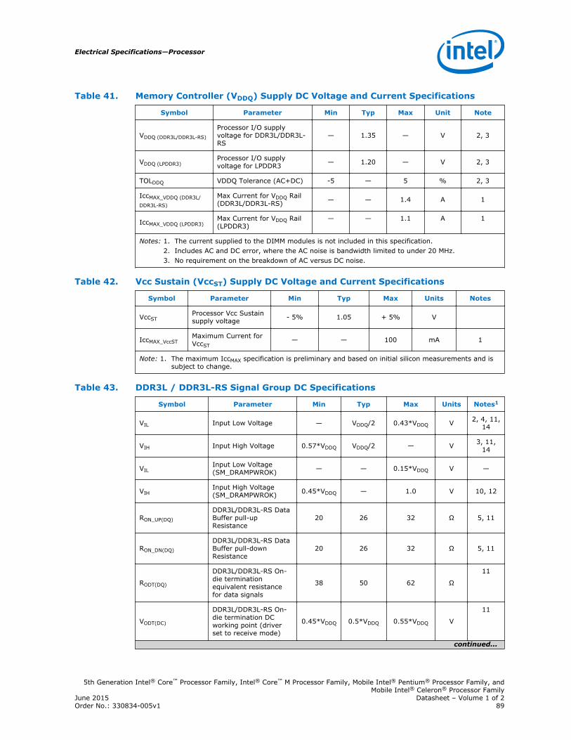
Table 41. Memory Controller (VDDQ) Supply DC Voltage and Current Specifications
Symbol Parameter Min Typ Max Unit Note
VDDQ (DDR3L/DDR3L-RS)
Processor I/O supplyvoltage for DDR3L/DDR3L-RS
— 1.35 — V 2, 3
VDDQ (LPDDR3)Processor I/O supplyvoltage for LPDDR3 — 1.20 — V 2, 3
TOLDDQ VDDQ Tolerance (AC+DC) -5 — 5 % 2, 3
IccMAX_VDDQ (DDR3L/DDR3L-RS)
Max Current for VDDQ Rail(DDR3L/DDR3L-RS) — — 1.4 A 1
IccMAX_VDDQ (LPDDR3)Max Current for VDDQ Rail(LPDDR3)
— — 1.1 A 1
Notes: 1. The current supplied to the DIMM modules is not included in this specification.2. Includes AC and DC error, where the AC noise is bandwidth limited to under 20 MHz.3. No requirement on the breakdown of AC versus DC noise.
Table 42. Vcc Sustain (VccST) Supply DC Voltage and Current Specifications
Symbol Parameter Min Typ Max Units Notes
VccSTProcessor Vcc Sustainsupply voltage - 5% 1.05 + 5% V
IccMAX_VccSTMaximum Current forVccST
— — 100 mA 1
Note: 1. The maximum IccMAX specification is preliminary and based on initial silicon measurements and issubject to change.
Table 43. DDR3L / DDR3L-RS Signal Group DC Specifications
Symbol Parameter Min Typ Max Units Notes1
VIL Input Low Voltage — VDDQ/2 0.43*VDDQ V 2, 4, 11,14
VIH Input High Voltage 0.57*VDDQ VDDQ/2 — V 3, 11,14
VILInput Low Voltage(SM_DRAMPWROK) — — 0.15*VDDQ V —
VIHInput High Voltage(SM_DRAMPWROK) 0.45*VDDQ — 1.0 V 10, 12
RON_UP(DQ)
DDR3L/DDR3L-RS DataBuffer pull-upResistance
20 26 32 Ω 5, 11
RON_DN(DQ)
DDR3L/DDR3L-RS DataBuffer pull-downResistance
20 26 32 Ω 5, 11
RODT(DQ)
DDR3L/DDR3L-RS On-die terminationequivalent resistancefor data signals
38 50 62 Ω
11
VODT(DC)
DDR3L/DDR3L-RS On-die termination DCworking point (driverset to receive mode)
0.45*VDDQ 0.5*VDDQ 0.55*VDDQ V
11
continued...
Electrical Specifications—Processor
5th Generation Intel® Core™ Processor Family, Intel® Core™ M Processor Family, Mobile Intel® Pentium® Processor Family, andMobile Intel® Celeron® Processor Family
June 2015 Datasheet – Volume 1 of 2Order No.: 330834-005v1 89
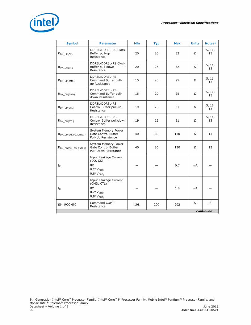
Symbol Parameter Min Typ Max Units Notes1
RON_UP(CK)
DDR3L/DDR3L-RS ClockBuffer pull-upResistance
20 26 32 Ω5, 11,
13
RON_DN(CK)
DDR3L/DDR3L-RS ClockBuffer pull-downResistance
20 26 32 Ω 5, 11,13
RON_UP(CMD)
DDR3L/DDR3L-RSCommand Buffer pull-up Resistance
15 20 25 Ω 5, 11,13
RON_DN(CMD)
DDR3L/DDR3L-RSCommand Buffer pull-down Resistance
15 20 25 Ω 5, 11,13
RON_UP(CTL)
DDR3L/DDR3L-RSControl Buffer pull-upResistance
19 25 31 Ω 5, 11,13
RON_DN(CTL)
DDR3L/DDR3L-RSControl Buffer pull-downResistance
19 25 31 Ω5, 11,
13
RON_UP(SM_PG_CNTL1)
System Memory PowerGate Control BufferPull-Up Resistance
40 80 130 Ω 13
RON_DN(SM_PG_CNTL1)
System Memory PowerGate Control BufferPull-Down Resistance
40 80 130 Ω 13
ILI
Input Leakage Current(DQ, CK)0V0.2*VDDQ
0.8*VDDQ
— — 0.7 mA —
ILI
Input Leakage Current(CMD, CTL)0V0.2*VDDQ
0.8*VDDQ
— — 1.0 mA —
SM_RCOMP0 Command COMPResistance 198 200 202 Ω 8
continued...
Processor—Electrical Specifications
5th Generation Intel® Core™ Processor Family, Intel® Core™ M Processor Family, Mobile Intel® Pentium® Processor Family, andMobile Intel® Celeron® Processor FamilyDatasheet – Volume 1 of 2 June 201590 Order No.: 330834-005v1

Symbol Parameter Min Typ Max Units Notes1
SM_RCOMP1 Data COMP Resistance 118.8 120 121.2 Ω 8
SM_RCOMP2 ODT COMP Resistance 99 100 101 Ω 8
Notes: 1. Unless otherwise noted, all specifications in this table apply to all processor frequencies.2. VIL is defined as the maximum voltage level at a receiving agent that will be interpreted as a
logical low value.3. VIH is defined as the minimum voltage level at a receiving agent that will be interpreted as a
logical high value.4. VIH and VOH may experience excursions above VDDQ. However, input signal drivers must comply
with the signal quality specifications.5. This is the pull up/down driver resistance.6. RTERM is the termination on the DIMM and in not controlled by the processor.7. The minimum and maximum values for these signals are programmable by BIOS to one of the
two sets.8. SM_RCOMPx resistance must be provided on the system board with 1% resistors. SM_RCOMPx
resistors are to VSS.9. SM_DRAMPWROK rise and fall time must be < 50 ns measured between VDDQ *0.15 and VDDQ
*0.47.10.SM_VREF is defined as VDDQ/2.11.Maximum-minimum range is correct; however, center point is subject to change during MRC
boot training.12.Processor may be damaged if VIH exceeds the maximum voltage for extended periods.13.The MRC during boot training might optimize RON outside the range specified.14.RON tolerance is preliminary and might be subject to change.
Table 44. LPDDR3 Signal Group DC Specifications
Symbol Parameter Min Typ. Max Unit Note
VIL Input Low Voltage — VDDQ /2 0.43*VDDQ V 2, 4, 11,12
VIH Input High Voltage 0.57*VDDQ VDDQ /2 — V 3, 11,12
VILInput Low Voltage(SM_DRAMPWROK) — — 0.15*VDDQ V —
VIHInput High Voltage(SM_DRAMPWROK) 0.45*VDDQ — 1.0*VDDQ V 10, 13
RON_UP(DQ)LPDDR3 Data Buffer pull-up Resistance 30 40 50 Ω 5, 12
RON_DN(DQ)LPDDR3 Data Buffer pull-down Resistance 30 40 50 Ω 5, 12
RODT(DQ)
LPDDR3 On-dietermination equivalentresistance for data signals
150 200 250 Ω 12
VODT(DC)
LPDDR3 On-dietermination DC workingpoint (driver set to receivemode)
0.45*VDDQ 0.5*VDDQ 0.55*VDDQ V 12
RON_UP(CK)LPDDR3 Clock Buffer pull-up Resistance 30 40 50 Ω 5, 12
RON_DN(CK)LPDDR3 Clock Buffer pull-down Resistance 30 40 50 Ω 5, 12
RON_UP(CMD)LPDDR3 Command Bufferpull-up Resistance 19 25 31 Ω 5, 12
continued...
Electrical Specifications—Processor
5th Generation Intel® Core™ Processor Family, Intel® Core™ M Processor Family, Mobile Intel® Pentium® Processor Family, andMobile Intel® Celeron® Processor Family
June 2015 Datasheet – Volume 1 of 2Order No.: 330834-005v1 91
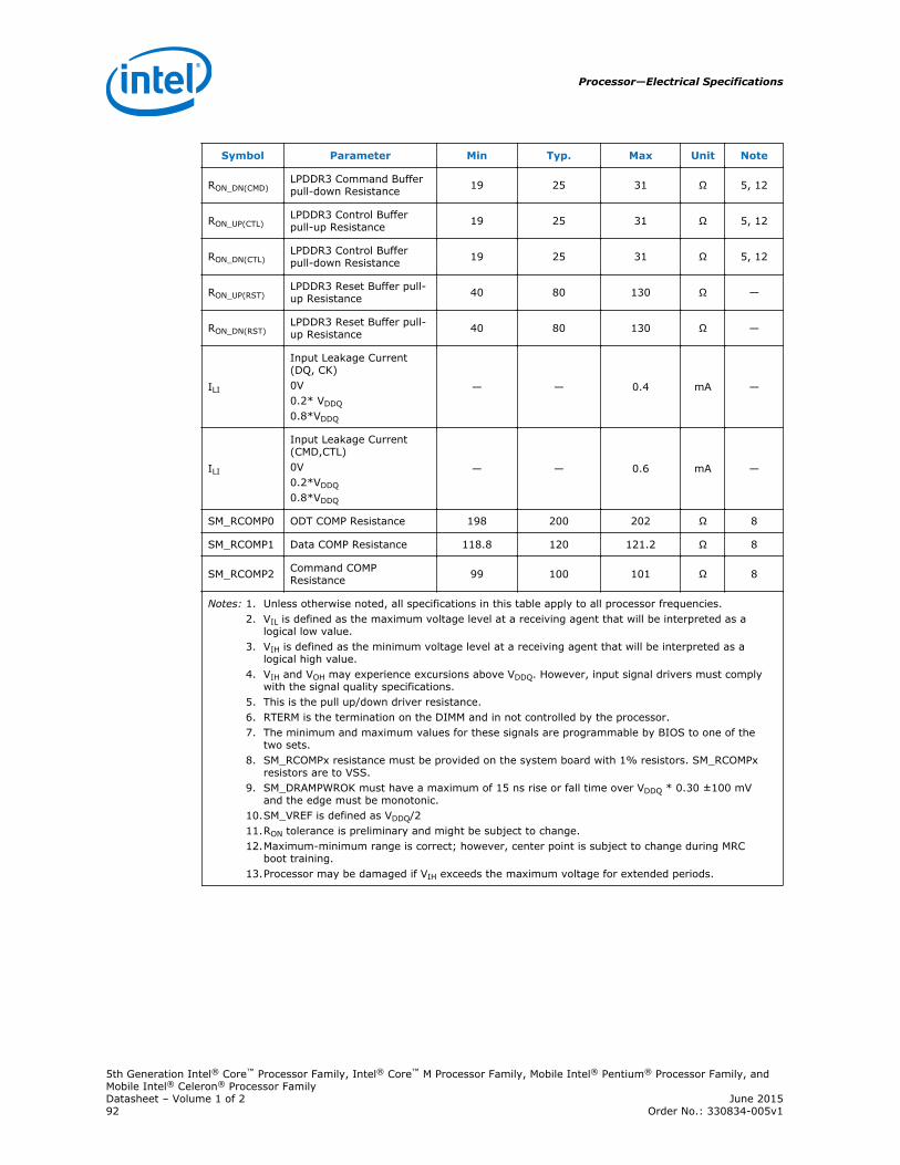
Symbol Parameter Min Typ. Max Unit Note
RON_DN(CMD)LPDDR3 Command Bufferpull-down Resistance 19 25 31 Ω 5, 12
RON_UP(CTL)LPDDR3 Control Bufferpull-up Resistance 19 25 31 Ω 5, 12
RON_DN(CTL)LPDDR3 Control Bufferpull-down Resistance 19 25 31 Ω 5, 12
RON_UP(RST)LPDDR3 Reset Buffer pull-up Resistance 40 80 130 Ω —
RON_DN(RST)LPDDR3 Reset Buffer pull-up Resistance 40 80 130 Ω —
ILI
Input Leakage Current(DQ, CK)0V0.2* VDDQ
0.8*VDDQ
— — 0.4 mA —
ILI
Input Leakage Current(CMD,CTL)0V0.2*VDDQ
0.8*VDDQ
— — 0.6 mA —
SM_RCOMP0 ODT COMP Resistance 198 200 202 Ω 8
SM_RCOMP1 Data COMP Resistance 118.8 120 121.2 Ω 8
SM_RCOMP2 Command COMPResistance 99 100 101 Ω 8
Notes: 1. Unless otherwise noted, all specifications in this table apply to all processor frequencies.2. VIL is defined as the maximum voltage level at a receiving agent that will be interpreted as a
logical low value.3. VIH is defined as the minimum voltage level at a receiving agent that will be interpreted as a
logical high value.4. VIH and VOH may experience excursions above VDDQ. However, input signal drivers must comply
with the signal quality specifications.5. This is the pull up/down driver resistance.6. RTERM is the termination on the DIMM and in not controlled by the processor.7. The minimum and maximum values for these signals are programmable by BIOS to one of the
two sets.8. SM_RCOMPx resistance must be provided on the system board with 1% resistors. SM_RCOMPx
resistors are to VSS.9. SM_DRAMPWROK must have a maximum of 15 ns rise or fall time over VDDQ * 0.30 ±100 mV
and the edge must be monotonic.10.SM_VREF is defined as VDDQ/211.RON tolerance is preliminary and might be subject to change.12.Maximum-minimum range is correct; however, center point is subject to change during MRC
boot training.13.Processor may be damaged if VIH exceeds the maximum voltage for extended periods.
Processor—Electrical Specifications
5th Generation Intel® Core™ Processor Family, Intel® Core™ M Processor Family, Mobile Intel® Pentium® Processor Family, andMobile Intel® Celeron® Processor FamilyDatasheet – Volume 1 of 2 June 201592 Order No.: 330834-005v1
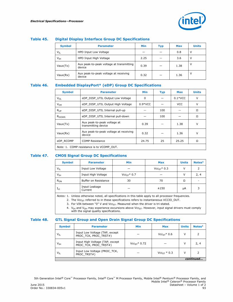
Table 45. Digital Display Interface Group DC Specifications
Symbol Parameter Min Typ Max Units
VIL HPD Input Low Voltage — — 0.8 V
VIH HPD Input High Voltage 2.25 — 3.6 V
Vaux(Tx) Aux peak-to-peak voltage at transmittingdevice 0.39 — 1.38 V
Vaux(Rx) Aux peak-to-peak voltage at receivingdevice 0.32 — 1.36 V
Table 46. Embedded DisplayPort* (eDP) Group DC Specifications
Symbol Parameter Min Typ Max Units
VOL eDP_DISP_UTIL Output Low Voltage 0 — 0.1*VCC V
VOH eDP_DISP_UTIL Output High Voltage 0.9*VCC — VCC V
RUP eDP_DISP_UTIL Internal pull-up — 100 — Ω
RDOWN eDP_DISP_UTIL Internal pull-down — 100 — Ω
Vaux(Tx) Aux peak-to-peak voltage attransmitting device 0.39 — 1.38 V
Vaux(Rx) Aux peak-to-peak voltage at receivingdevice 0.32 — 1.36 V
eDP_RCOMP COMP Resistance 24.75 25 25.25 Ω
Note: 1. COMP resistance is to VCOMP_OUT.
Table 47. CMOS Signal Group DC Specifications
Symbol Parameter Min Max Units Notes1
VIL Input Low Voltage — VccST* 0.3 V 2
VIH Input High Voltage VccST* 0.7 — V 2, 4
RON Buffer on Resistance 30 70 Ω -
ILIInput LeakageCurrent — ±150 μA 3
Notes: 1. Unless otherwise noted, all specifications in this table apply to all processor frequencies.2. The VccST referred to in these specifications refers to instantaneous VCCIO_OUT.3. For VIN between “0” V and VccST. Measured when the driver is tri-stated.4. VIH and VOH may experience excursions above VccST. However, input signal drivers must comply
with the signal quality specifications.
Table 48. GTL Signal Group and Open Drain Signal Group DC Specifications
Symbol Parameter Min Max Units Notes1
VILInput Low Voltage (TAP, exceptPROC_TCK, PROC_TRST#) — VccST* 0.6 V 2
VIHInput High Voltage (TAP, exceptPROC_TCK, PROC_TRST#) VccST* 0.72 — V 2, 4
VILInput Low Voltage (PROC_TCK,PROC_TRST#) — VccST * 0.3 V 2
continued...
Electrical Specifications—Processor
5th Generation Intel® Core™ Processor Family, Intel® Core™ M Processor Family, Mobile Intel® Pentium® Processor Family, andMobile Intel® Celeron® Processor Family
June 2015 Datasheet – Volume 1 of 2Order No.: 330834-005v1 93
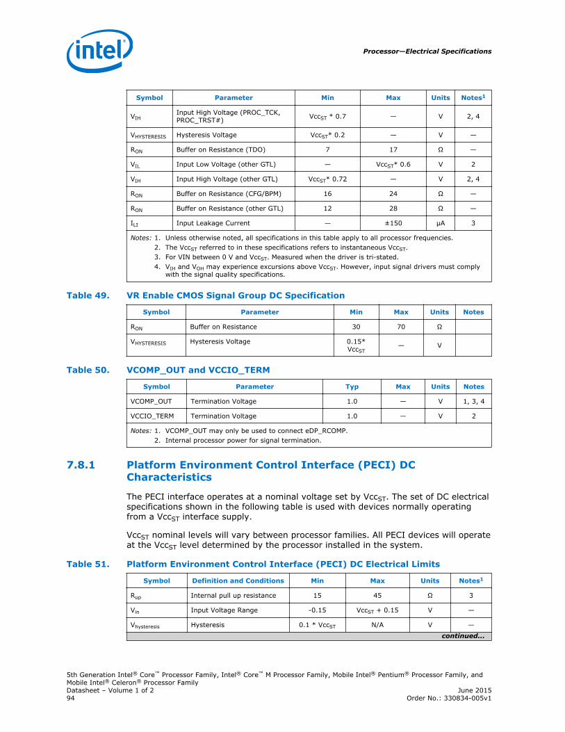
Symbol Parameter Min Max Units Notes1
VIHInput High Voltage (PROC_TCK,PROC_TRST#) VccST * 0.7 — V 2, 4
VHYSTERESIS Hysteresis Voltage VccST* 0.2 — V —
RON Buffer on Resistance (TDO) 7 17 Ω —
VIL Input Low Voltage (other GTL) — VccST* 0.6 V 2
VIH Input High Voltage (other GTL) VccST* 0.72 — V 2, 4
RON Buffer on Resistance (CFG/BPM) 16 24 Ω —
RON Buffer on Resistance (other GTL) 12 28 Ω —
ILI Input Leakage Current — ±150 μA 3
Notes: 1. Unless otherwise noted, all specifications in this table apply to all processor frequencies.2. The VccST referred to in these specifications refers to instantaneous VccST.3. For VIN between 0 V and VccST. Measured when the driver is tri-stated.4. VIH and VOH may experience excursions above VccST. However, input signal drivers must comply
with the signal quality specifications.
Table 49. VR Enable CMOS Signal Group DC Specification
Symbol Parameter Min Max Units Notes
RON Buffer on Resistance 30 70 Ω
VHYSTERESIS Hysteresis Voltage 0.15*VccST
— V
Table 50. VCOMP_OUT and VCCIO_TERM
Symbol Parameter Typ Max Units Notes
VCOMP_OUT Termination Voltage 1.0 — V 1, 3, 4
VCCIO_TERM Termination Voltage 1.0 — V 2
Notes: 1. VCOMP_OUT may only be used to connect eDP_RCOMP.2. Internal processor power for signal termination.
Platform Environment Control Interface (PECI) DCCharacteristics
The PECI interface operates at a nominal voltage set by VccST. The set of DC electricalspecifications shown in the following table is used with devices normally operatingfrom a VccST interface supply.
VccST nominal levels will vary between processor families. All PECI devices will operateat the VccST level determined by the processor installed in the system.
Table 51. Platform Environment Control Interface (PECI) DC Electrical Limits
Symbol Definition and Conditions Min Max Units Notes1
Rup Internal pull up resistance 15 45 Ω 3
Vin Input Voltage Range -0.15 VccST + 0.15 V —
Vhysteresis Hysteresis 0.1 * VccST N/A V —
continued...
7.8.1
Processor—Electrical Specifications
5th Generation Intel® Core™ Processor Family, Intel® Core™ M Processor Family, Mobile Intel® Pentium® Processor Family, andMobile Intel® Celeron® Processor FamilyDatasheet – Volume 1 of 2 June 201594 Order No.: 330834-005v1

Symbol Definition and Conditions Min Max Units Notes1
VnNegative-Edge ThresholdVoltage 0.275 * VccST 0.525 * VccST V —
VpPositive-Edge ThresholdVoltage 0.550 * VccST 0.725 * VccST V —
Cbus Bus Capacitance per Node N/A 10 pF —
Cpad Pad Capacitance 0.7 1.8 pF —
Ileak000 leakage current at 0 V — 0.6 mA —
Ileak025 leakage current at 0.25*VccST
— 0.4 mA —
Ileak050 leakage current at 0.50*VccST
— 0.2 mA —
Ileak075 leakage current at 0.75*VccST
— 0.13 mA —
Ileak100 leakage current at VccST — 0.10 mA —
Notes: 1. VccST supplies the PECI interface. PECI behavior does not affect VccST minimum / maximumspecifications.
2. The leakage specification applies to powered devices on the PECI bus.3. The PECI buffer internal pull-up resistance measured at 0.75* VccST.
Input Device Hysteresis
The input buffers in both client and host models must use a Schmitt-triggered inputdesign for improved noise immunity. Use the following figure as a guide for inputbuffer design.
Figure 13. Input Device Hysteresis
Minimum VP
Maximum VP
Minimum VN
Maximum VN
PECI High Range
PECI Low Range
Valid InputSignal Range
MinimumHysteresis
VTTD
PECI Ground
7.8.2
Electrical Specifications—Processor
5th Generation Intel® Core™ Processor Family, Intel® Core™ M Processor Family, Mobile Intel® Pentium® Processor Family, andMobile Intel® Celeron® Processor Family
June 2015 Datasheet – Volume 1 of 2Order No.: 330834-005v1 95
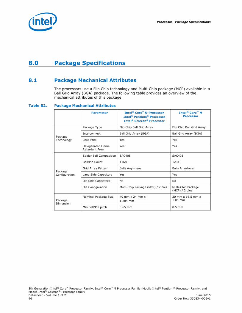
8.0 Package Specifications
Package Mechanical Attributes
The processors use a Flip Chip technology and Multi-Chip package (MCP) available in aBall Grid Array (BGA) package. The following table provides an overview of themechanical attributes of this package.
Table 52. Package Mechanical Attributes
Parameter Intel® Core™ U-ProcessorIntel® Pentium® ProcessorIntel® Celeron® Processor
Intel® Core™ MProcessor
PackageTechnology
Package Type Flip Chip Ball Grid Array Flip Chip Ball Grid Array
Interconnect Ball Grid Array (BGA) Ball Grid Array (BGA)
Lead Free Yes Yes
Halogenated FlameRetardant Free
Yes Yes
PackageConfiguration
Solder Ball Composition SAC405 SAC405
Ball/Pin Count 1168 1234
Grid Array Pattern Balls Anywhere Balls Anywhere
Land Side Capacitors Yes Yes
Die Side Capacitors No No
Die Configuration Multi-Chip Package (MCP) / 2 dies Multi-Chip Package(MCP) / 2 dies
PackageDimension
Nominal Package Size 40 mm x 24 mm x1.284 mm
30 mm x 16.5 mm x1.05 mm
Min Ball/Pin pitch 0.65 mm 0.5 mm
8.1
Processor—Package Specifications
5th Generation Intel® Core™ Processor Family, Intel® Core™ M Processor Family, Mobile Intel® Pentium® Processor Family, andMobile Intel® Celeron® Processor FamilyDatasheet – Volume 1 of 2 June 201596 Order No.: 330834-005v1

Package Loading Specifications
Table 53. Package Loading Specifications
Maximum Static Normal Load Limit Notes
U-Processor Line 67 N (15 lbf) 1, 2, 3
Intel® Core™ M Processor Family 44 N (10 lbf) 1, 2, 3
Notes: 1. The thermal solution attach mechanism must not induce continuous stress to the package. Itmay only apply a uniform load to the die to maintain a thermal interface.
2. This specification applies to the uniform compressive load in the direction perpendicular to thedies’ top surface.
3. This specification is based on limited testing for design characterization.4. Assumes a motherboard thickness of 1.0 mm or greater.5. Assumes the use of a backing plate.
Package Storage Specifications
Table 54. Package Storage Specifications
Parameter Description Min Max Notes
TABSOLUTE STORAGE
The non-operating device storage temperature.Damage (latent or otherwise) may occur whensubjected to this temperature for any length oftime.
-25 °C 125 °C 1, 2, 3
TSUSTAINED STORAGEThe ambient storage temperature limit (inshipping media) for a sustained period of time. -5 °C 40 °C 4, 5
RHSUSTAINED STORAGEThe maximum device storage relative humidity fora sustained period of time. 60% @ 24 °C 5, 6
TIMESUSTAINED STORAGEA prolonged or extended period of time: typicallyassociated with customer shelf life.
0months
6months 6
Notes: 1. Refers to a component device that is not assembled in a board or socket that is not to beelectrically connected to a voltage reference or I/O signals.
2. Specified temperatures are based on data collected. Exceptions for surface mount reflow arespecified by applicable JEDEC standards.
3. TABSOLUTE STORAGE applies to the unassembled component only and does not apply to the shippingmedia, moisture barrier bags or desiccant.
4. Intel-branded board products are certified to meet the following temperature and humidity limitsthat are given as an example only (Non-Operating Temperature Limit: -40 °C to 70 °C, Humidity50% to 90%, non-condensing with a maximum wet bulb of 28 °C). Post board attach storagetemperature limits are not specified for non-Intel branded boards.
5. The JEDEC, J-JSTD-020 moisture level rating and associated handling practices apply to allmoisture sensitive devices removed from the moisture barrier bag.
6. Nominal temperature and humidity conditions and durations are given and tested within theconstraints imposed by TSUSTAINED STORAGE and customer shelf life in applicable Intel boxes andbags.
8.2
8.3
Package Specifications—Processor
5th Generation Intel® Core™ Processor Family, Intel® Core™ M Processor Family, Mobile Intel® Pentium® Processor Family, andMobile Intel® Celeron® Processor Family
June 2015 Datasheet – Volume 1 of 2Order No.: 330834-005v1 97
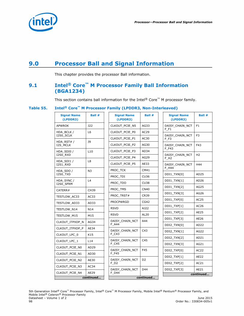
9.0 Processor Ball and Signal Information
This chapter provides the processor Ball information.
Intel® Core™ M Processor Family Ball Information(BGA1234)
This section contains ball information for the Intel® Core™ M processor family.
Table 55. Intel® Core™ M Processor Family (LPDDR3, Non-Interleaved)
Signal Name(LPDDR3)
Ball #
APWROK J22
HDA_BCLK /I2S0_SCLK
L6
HDA_RST# /I2S_MCLK
J9
HDA_SDI0 /I2S0_RXD
L10
HDA_SDI1 /I2S1_RXD
L8
HDA_SDO /I2S0_TXD
N3
HDA_SYNC /I2S0_SFRM
L4
CATERR# CH39
TESTLOW_AC33 AC33
TESTLOW_AD33 AD33
TESTLOW_N14 N14
TESTLOW_M15 M15
CLKOUT_ITPXDP_N AG34
CLKOUT_ITPXDP_P AE34
CLKOUT_LPC_0 K15
CLKOUT_LPC_1 L14
CLKOUT_PCIE_N0 AD29
CLKOUT_PCIE_N1 AD30
CLKOUT_PCIE_N2 AE30
CLKOUT_PCIE_N3 AC34
CLKOUT_PCIE_N4 AE29
continued...
Signal Name(LPDDR3)
Ball #
CLKOUT_PCIE_N5 AG33
CLKOUT_PCIE_P0 AC29
CLKOUT_PCIE_P1 AC30
CLKOUT_PCIE_P2 AG30
CLKOUT_PCIE_P3 AD34
CLKOUT_PCIE_P4 AG29
CLKOUT_PCIE_P5 AE33
PROC_TCK CM41
PROC_TDI CU36
PROC_TDO CU38
PROC_TMS CN40
PROC_TRST# CR39
PROCPWRGD CG42
RSVD AJ22
RSVD AL20
DAISY_CHAIN_NCTF_A44
A44
DAISY_CHAIN_NCTF_C43
C43
DAISY_CHAIN_NCTF_C45
C45
DAISY_CHAIN_NCTF_F45
F45
DAISY_CHAIN_NCTF_D2
D2
DAISY_CHAIN_NCTF_D44
D44
continued...
Signal Name(LPDDR3)
Ball #
DAISY_CHAIN_NCTF_F1
F1
DAISY_CHAIN_NCTF_F3
F3
DAISY_CHAIN_NCTF_F43
F43
DAISY_CHAIN_NCTF_H2
H2
DAISY_CHAIN_NCTF_H44
H44
DDI1_TXN[0] AD25
DDI1_TXN[1] AD26
DDI1_TXN[2] AG25
DDI1_TXN[3] AG26
DDI1_TXP[0] AC25
DDI1_TXP[1] AC26
DDI1_TXP[2] AE25
DDI1_TXP[3] AE26
DDI2_TXN[0] AD22
DDI2_TXN[1] AG22
DDI2_TXN[2] AD21
DDI2_TXN[3] AG21
DDI2_TXP[0] AC22
DDI2_TXP[1] AE22
DDI2_TXP[2] AC21
DDI2_TXP[3] AE21
continued...
9.1
Processor—Processor Ball and Signal Information
5th Generation Intel® Core™ Processor Family, Intel® Core™ M Processor Family, Mobile Intel® Pentium® Processor Family, andMobile Intel® Celeron® Processor FamilyDatasheet – Volume 1 of 2 June 201598 Order No.: 330834-005v1
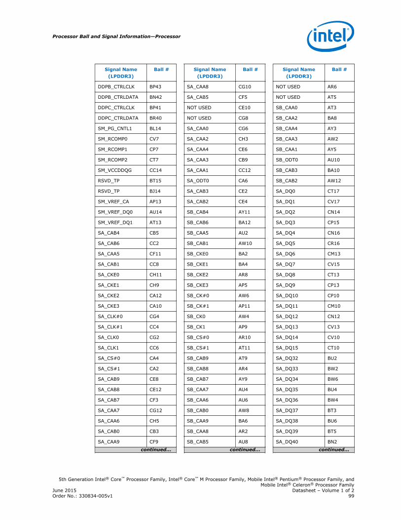
Signal Name(LPDDR3)
Ball #
DDPB_CTRLCLK BP43
DDPB_CTRLDATA BN42
DDPC_CTRLCLK BP41
DDPC_CTRLDATA BR40
SM_PG_CNTL1 BL14
SM_RCOMP0 CV7
SM_RCOMP1 CP7
SM_RCOMP2 CT7
SM_VCCDDQG CC14
RSVD_TP BT15
RSVD_TP BJ14
SM_VREF_CA AP13
SM_VREF_DQ0 AU14
SM_VREF_DQ1 AT13
SA_CAB4 CB5
SA_CAB6 CC2
SA_CAA5 CF11
SA_CAB1 CC8
SA_CKE0 CH11
SA_CKE1 CH9
SA_CKE2 CA12
SA_CKE3 CA10
SA_CLK#0 CG4
SA_CLK#1 CC4
SA_CLK0 CG2
SA_CLK1 CC6
SA_CS#0 CA4
SA_CS#1 CA2
SA_CAB9 CE8
SA_CAB8 CE12
SA_CAB7 CF3
SA_CAA7 CG12
SA_CAA6 CH5
SA_CAB0 CB3
SA_CAA9 CF9
continued...
Signal Name(LPDDR3)
Ball #
SA_CAA8 CG10
SA_CAB5 CF5
NOT USED CE10
NOT USED CG8
SA_CAA0 CG6
SA_CAA2 CH3
SA_CAA4 CE6
SA_CAA3 CB9
SA_CAA1 CC12
SA_ODT0 CA6
SA_CAB3 CE2
SA_CAB2 CE4
SB_CAB4 AY11
SB_CAB6 BA12
SB_CAA5 AU2
SB_CAB1 AW10
SB_CKE0 BA2
SB_CKE1 BA4
SB_CKE2 AR8
SB_CKE3 AP5
SB_CK#0 AW6
SB_CK#1 AP11
SB_CK0 AW4
SB_CK1 AP9
SB_CS#0 AR10
SB_CS#1 AT11
SB_CAB9 AT9
SB_CAB8 AR4
SB_CAB7 AY9
SB_CAA7 AU4
SB_CAA6 AU6
SB_CAB0 AW8
SB_CAA9 BA6
SB_CAA8 AR2
SB_CAB5 AU8
continued...
Signal Name(LPDDR3)
Ball #
NOT USED AR6
NOT USED AT5
SB_CAA0 AT3
SB_CAA2 BA8
SB_CAA4 AY3
SB_CAA3 AW2
SB_CAA1 AY5
SB_ODT0 AU10
SB_CAB3 BA10
SB_CAB2 AW12
SA_DQ0 CT17
SA_DQ1 CV17
SA_DQ2 CN14
SA_DQ3 CP15
SA_DQ4 CN16
SA_DQ5 CR16
SA_DQ6 CM13
SA_DQ7 CV15
SA_DQ8 CT13
SA_DQ9 CP13
SA_DQ10 CP10
SA_DQ11 CM10
SA_DQ12 CN12
SA_DQ13 CV13
SA_DQ14 CV10
SA_DQ15 CT10
SA_DQ32 BU2
SA_DQ33 BW2
SA_DQ34 BW6
SA_DQ35 BU4
SA_DQ36 BW4
SA_DQ37 BT3
SA_DQ38 BU6
SA_DQ39 BT5
SA_DQ40 BN2
continued...
Processor Ball and Signal Information—Processor
5th Generation Intel® Core™ Processor Family, Intel® Core™ M Processor Family, Mobile Intel® Pentium® Processor Family, andMobile Intel® Celeron® Processor Family
June 2015 Datasheet – Volume 1 of 2Order No.: 330834-005v1 99
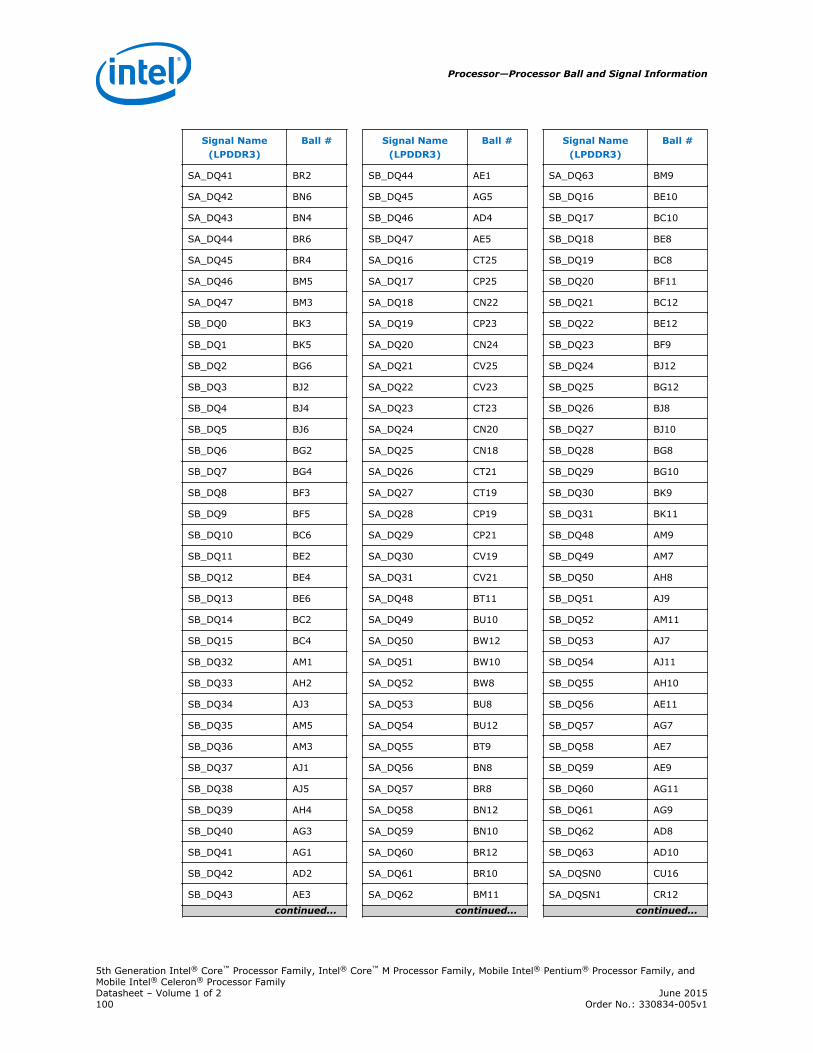
Signal Name(LPDDR3)
Ball #
SA_DQ41 BR2
SA_DQ42 BN6
SA_DQ43 BN4
SA_DQ44 BR6
SA_DQ45 BR4
SA_DQ46 BM5
SA_DQ47 BM3
SB_DQ0 BK3
SB_DQ1 BK5
SB_DQ2 BG6
SB_DQ3 BJ2
SB_DQ4 BJ4
SB_DQ5 BJ6
SB_DQ6 BG2
SB_DQ7 BG4
SB_DQ8 BF3
SB_DQ9 BF5
SB_DQ10 BC6
SB_DQ11 BE2
SB_DQ12 BE4
SB_DQ13 BE6
SB_DQ14 BC2
SB_DQ15 BC4
SB_DQ32 AM1
SB_DQ33 AH2
SB_DQ34 AJ3
SB_DQ35 AM5
SB_DQ36 AM3
SB_DQ37 AJ1
SB_DQ38 AJ5
SB_DQ39 AH4
SB_DQ40 AG3
SB_DQ41 AG1
SB_DQ42 AD2
SB_DQ43 AE3
continued...
Signal Name(LPDDR3)
Ball #
SB_DQ44 AE1
SB_DQ45 AG5
SB_DQ46 AD4
SB_DQ47 AE5
SA_DQ16 CT25
SA_DQ17 CP25
SA_DQ18 CN22
SA_DQ19 CP23
SA_DQ20 CN24
SA_DQ21 CV25
SA_DQ22 CV23
SA_DQ23 CT23
SA_DQ24 CN20
SA_DQ25 CN18
SA_DQ26 CT21
SA_DQ27 CT19
SA_DQ28 CP19
SA_DQ29 CP21
SA_DQ30 CV19
SA_DQ31 CV21
SA_DQ48 BT11
SA_DQ49 BU10
SA_DQ50 BW12
SA_DQ51 BW10
SA_DQ52 BW8
SA_DQ53 BU8
SA_DQ54 BU12
SA_DQ55 BT9
SA_DQ56 BN8
SA_DQ57 BR8
SA_DQ58 BN12
SA_DQ59 BN10
SA_DQ60 BR12
SA_DQ61 BR10
SA_DQ62 BM11
continued...
Signal Name(LPDDR3)
Ball #
SA_DQ63 BM9
SB_DQ16 BE10
SB_DQ17 BC10
SB_DQ18 BE8
SB_DQ19 BC8
SB_DQ20 BF11
SB_DQ21 BC12
SB_DQ22 BE12
SB_DQ23 BF9
SB_DQ24 BJ12
SB_DQ25 BG12
SB_DQ26 BJ8
SB_DQ27 BJ10
SB_DQ28 BG8
SB_DQ29 BG10
SB_DQ30 BK9
SB_DQ31 BK11
SB_DQ48 AM9
SB_DQ49 AM7
SB_DQ50 AH8
SB_DQ51 AJ9
SB_DQ52 AM11
SB_DQ53 AJ7
SB_DQ54 AJ11
SB_DQ55 AH10
SB_DQ56 AE11
SB_DQ57 AG7
SB_DQ58 AE7
SB_DQ59 AE9
SB_DQ60 AG11
SB_DQ61 AG9
SB_DQ62 AD8
SB_DQ63 AD10
SA_DQSN0 CU16
SA_DQSN1 CR12
continued...
Processor—Processor Ball and Signal Information
5th Generation Intel® Core™ Processor Family, Intel® Core™ M Processor Family, Mobile Intel® Pentium® Processor Family, andMobile Intel® Celeron® Processor FamilyDatasheet – Volume 1 of 2 June 2015100 Order No.: 330834-005v1
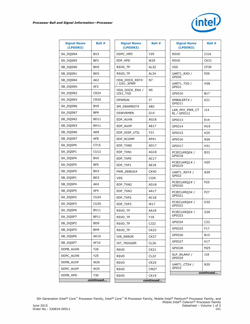
Signal Name(LPDDR3)
Ball #
SA_DQSN4 BV3
SA_DQSN5 BP3
SB_DQSN0 BH5
SB_DQSN1 BD5
SB_DQSN4 AK2
SB_DQSN5 AF2
SA_DQSN2 CR24
SA_DQSN3 CR20
SA_DQSN6 BV9
SA_DQSN7 BP9
SB_DQSN2 BD11
SB_DQSN3 BH11
SB_DQSN6 AK8
SB_DQSN7 AF8
SA_DQSP0 CT15
SA_DQSP1 CU12
SA_DQSP4 BV5
SA_DQSP5 BP5
SB_DQSP0 BH3
SB_DQSP1 BD3
SB_DQSP4 AK4
SB_DQSP5 AF4
SA_DQSP2 CU24
SA_DQSP3 CU20
SA_DQSP6 BV11
SA_DQSP7 BP11
SB_DQSP2 BD9
SB_DQSP3 BH9
SB_DQSP6 AK10
SB_DQSP7 AF10
DDPB_AUXN Y26
DDPC_AUXN Y25
DDPB_AUXP W26
DDPC_AUXP W25
DDPB_HPD Y30
continued...
Signal Name(LPDDR3)
Ball #
DDPC_HPD Y29
EDP_HPD W29
RSVD_TP AL32
RSVD_TP AL34
HDA_DOCK_RST#/ I2S1_SFRM
N7
HDA_DOCK_EN# /I2S1_TXD
N5
DPWROK J7
SM_DRAMRST# AB2
DSWVRMEN G14
EDP_AUXN AG16
EDP_AUXP AE17
EDP_DISP_UTIL Y21
EDP_RCOMP AP41
EDP_TXN0 AD17
EDP_TXN1 AG18
EDP_TXP0 AC17
EDP_TXP1 AE18
PWR_DEBUG# CK40
VSS CJ20
EDP_TXN2 AD18
EDP_TXN3 AA17
EDP_TXP2 AC18
EDP_TXP3 W17
RSVD_TP AA18
RSVD_TP Y18
RSVD_TP CJ22
RSVD_TP CK23
IVR_ERROR CK27
IST_TRIGGER CL26
RSVD CK21
RSVD CL22
RSVD CK25
RSVD CM27
RSVD CK19
continued...
Signal Name(LPDDR3)
Ball #
RSVD CJ16
RSVD CK31
VSS CF39
UART1_RXD /GPIO0
P29
UART1_TXD /GPIO1
H38
GPIO10 B17
SMBALERT# /GPIO11
K21
LAN_PHY_PWR_CTRL / GPIO12
J14
GPIO13 E14
GPIO14 M19
GPIO15 K25
GPIO16 N26
GPIO17 H31
PCIECLKRQ0# /GPIO18
B33
PCIECLKRQ1# /GPIO19
H25
UART1_RST# /GPIO2
N39
PCIECLKRQ2# /GPIO20
P25
PCIECLKRQ3# /GPIO21
P27
PCIECLKRQ4# /GPIO22
D35
PCIECLKRQ5# /GPIO23
G30
GPIO24 C22
GPIO25 F17
GPIO26 B15
GPIO27 K17
GPIO28 M25
SLP_WLAN# /GPIO29
J18
UART1_CTS# /GPIO3
N30
continued...
Processor Ball and Signal Information—Processor
5th Generation Intel® Core™ Processor Family, Intel® Core™ M Processor Family, Mobile Intel® Pentium® Processor Family, andMobile Intel® Celeron® Processor Family
June 2015 Datasheet – Volume 1 of 2Order No.: 330834-005v1 101
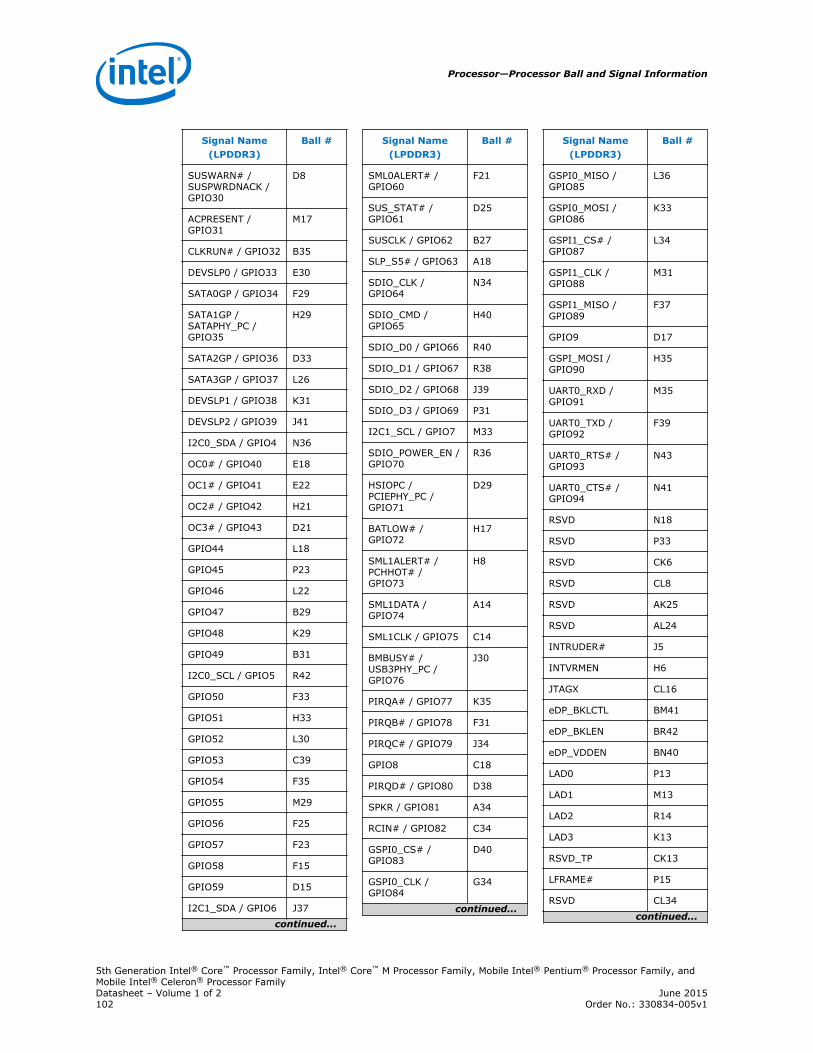
Signal Name(LPDDR3)
Ball #
SUSWARN# /SUSPWRDNACK /GPIO30
D8
ACPRESENT /GPIO31
M17
CLKRUN# / GPIO32 B35
DEVSLP0 / GPIO33 E30
SATA0GP / GPIO34 F29
SATA1GP /SATAPHY_PC /GPIO35
H29
SATA2GP / GPIO36 D33
SATA3GP / GPIO37 L26
DEVSLP1 / GPIO38 K31
DEVSLP2 / GPIO39 J41
I2C0_SDA / GPIO4 N36
OC0# / GPIO40 E18
OC1# / GPIO41 E22
OC2# / GPIO42 H21
OC3# / GPIO43 D21
GPIO44 L18
GPIO45 P23
GPIO46 L22
GPIO47 B29
GPIO48 K29
GPIO49 B31
I2C0_SCL / GPIO5 R42
GPIO50 F33
GPIO51 H33
GPIO52 L30
GPIO53 C39
GPIO54 F35
GPIO55 M29
GPIO56 F25
GPIO57 F23
GPIO58 F15
GPIO59 D15
I2C1_SDA / GPIO6 J37
continued...
Signal Name(LPDDR3)
Ball #
SML0ALERT# /GPIO60
F21
SUS_STAT# /GPIO61
D25
SUSCLK / GPIO62 B27
SLP_S5# / GPIO63 A18
SDIO_CLK /GPIO64
N34
SDIO_CMD /GPIO65
H40
SDIO_D0 / GPIO66 R40
SDIO_D1 / GPIO67 R38
SDIO_D2 / GPIO68 J39
SDIO_D3 / GPIO69 P31
I2C1_SCL / GPIO7 M33
SDIO_POWER_EN /GPIO70
R36
HSIOPC /PCIEPHY_PC /GPIO71
D29
BATLOW# /GPIO72
H17
SML1ALERT# /PCHHOT# /GPIO73
H8
SML1DATA /GPIO74
A14
SML1CLK / GPIO75 C14
BMBUSY# /USB3PHY_PC /GPIO76
J30
PIRQA# / GPIO77 K35
PIRQB# / GPIO78 F31
PIRQC# / GPIO79 J34
GPIO8 C18
PIRQD# / GPIO80 D38
SPKR / GPIO81 A34
RCIN# / GPIO82 C34
GSPI0_CS# /GPIO83
D40
GSPI0_CLK /GPIO84
G34
continued...
Signal Name(LPDDR3)
Ball #
GSPI0_MISO /GPIO85
L36
GSPI0_MOSI /GPIO86
K33
GSPI1_CS# /GPIO87
L34
GSPI1_CLK /GPIO88
M31
GSPI1_MISO /GPIO89
F37
GPIO9 D17
GSPI_MOSI /GPIO90
H35
UART0_RXD /GPIO91
M35
UART0_TXD /GPIO92
F39
UART0_RTS# /GPIO93
N43
UART0_CTS# /GPIO94
N41
RSVD N18
RSVD P33
RSVD CK6
RSVD CL8
RSVD AK25
RSVD AL24
INTRUDER# J5
INTVRMEN H6
JTAGX CL16
eDP_BKLCTL BM41
eDP_BKLEN BR42
eDP_VDDEN BN40
LAD0 P13
LAD1 M13
LAD2 R14
LAD3 K13
RSVD_TP CK13
LFRAME# P15
RSVD CL34
continued...
Processor—Processor Ball and Signal Information
5th Generation Intel® Core™ Processor Family, Intel® Core™ M Processor Family, Mobile Intel® Pentium® Processor Family, andMobile Intel® Celeron® Processor FamilyDatasheet – Volume 1 of 2 June 2015102 Order No.: 330834-005v1
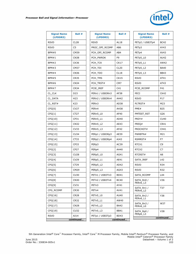
Signal Name(LPDDR3)
Ball #
RSVD CL28
RSVD C5
BPM#0 CM39
BPM#1 CN38
BPM#2 CK36
BPM#3 CM37
BPM#4 CN36
BPM#5 CR35
BPM#6 CN34
BPM#7 CR34
CL_CLK D23
CL_DATA H23
CL_RST# K23
CFG[0] CV27
CFG[1] CT27
CFG[10] CP31
CFG[11] CN32
CFG[12] CV33
CFG[13] CU34
CFG[14] CT33
CFG[15] CP33
CFG[2] CP27
CFG[3] CU28
CFG[4] CV29
CFG[5] CT29
CFG[6] CM29
CFG[7] CU30
CFG[8] CN30
CFG[9] CV31
CFG_RCOMP CR30
CFG[16] CR28
CFG[18] CR32
CFG[17] CN28
CFG[19] CU32
RSVD AJ14
continued...
Signal Name(LPDDR3)
Ball #
RSVD AL18
PROC_OPI_RCOMP AB6
PCH_OPI_RCOMP AB4
PCH_PWROK F9
PCH_TCK CK17
PCH_TDI CL20
PCH_TDO CL18
PCH_TMS CK15
PCH_TRST# CM7
PCIE_IREF C41
PERn1 / USB3Rn3 AF38
PERn2 / USB3Rn4 AH42
PERn3 AD38
PERn4 AH38
PERn5_L0 AF40
PERn5_L1 AD40
PERn5_L2 AE43
PERn5_L3 AF42
PERp1 / USB3Rp3 AE39
PERp2 / USB3Rp4 AJ43
PERp3 AC39
PERp4 AH40
PERp5_L0 AG41
PERp5_L1 AE41
PERp5_L2 AD42
PERp5_L3 AG43
PETn1 / USB3Tn3 BD41
PETn2 / USB3Tn4 BC40
PETn3 AY41
PETn4 AV41
PETn5_L0 AU40
PETn5_L1 AW40
PETn5_L2 BA42
PETn5_L3 BB41
PETp1 / USB3Tp3 BD43
continued...
Signal Name(LPDDR3)
Ball #
PETp2 / USB3Tp4 BC42
PETp3 AY43
PETp4 AV43
PETp5_L0 AU42
PETp5_L1 AW42
PETp5_L2 BA40
PETp5_L3 BB43
RSVD AT41
RSVD AT43
PCIE_RCOMP F41
PECI CK42
RSVD P17
PLTRST# M23
PME# B25
PMTEST_RST G26
PRDY# CU40
PREQ# CR41
PROCHOT# CH41
PWRBTN# M21
RSMRST# F7
RTCX1 C9
RTCX2 C7
RTCRST# A8
SATA_IREF L42
RSVD R34
RSVD R32
SATA_RCOMP L44
SATA_Rn0 /PERn6_L3
V36
SATA_Rn1 /PERn6_L2
T37
SATA_Rn2 /PERn6_L1
Y38
SATA_Rn3 /PERn6_L0
W37
SATA_Rp0 /PERp6_L3
V38
continued...
Processor Ball and Signal Information—Processor
5th Generation Intel® Core™ Processor Family, Intel® Core™ M Processor Family, Mobile Intel® Pentium® Processor Family, andMobile Intel® Celeron® Processor Family
June 2015 Datasheet – Volume 1 of 2Order No.: 330834-005v1 103
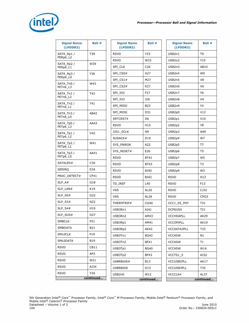
Signal Name(LPDDR3)
Ball #
SATA_Rp1 /PERp6_L2
T39
SATA_Rp2 /PERp6_L1
W39
SATA_Rp3 /PERp6_L0
Y36
SATA_Tn0 /PETn6_L3
W43
SATA_Tn1 /PETn6_L2
T43
SATA_Tn2 /PETn6_L1
T41
SATA_Tn3 /PETn6_L0
AB42
SATA_Tp0 /PETp6_L3
AA43
SATA_Tp1 /PETp6_L2
V42
SATA_Tp2 /PETp6_L1
W41
SATA_Tp3 /PETp6_L0
AA41
SATALED# C30
SERIRQ E34
PROC_DETECT# CF41
SLP_A# G18
SLP_LAN# K19
SLP_S0# G22
SLP_S3# N22
SLP_S4# H19
SLP_SUS# D27
SMBCLK P21
SMBDATA B21
SML0CLK P19
SML0DATA B19
RSVD CB11
RSVD AP3
RSVD W21
RSVD AJ34
RSVD Y34
continued...
Signal Name(LPDDR3)
Ball #
RSVD Y33
RSVD W33
SPI_CLK C26
SPI_CS0# H27
SPI_CS1# M27
SPI_CS2# K27
SPI_IO2 F27
SPI_IO3 J26
SPI_MISO B23
SPI_MOSI D31
SRTCRST# D6
RSVD H15
I2S1_SCLK N9
SUSACK# D19
SYS_PWROK A22
SYS_RESET# E26
RSVD BT41
RSVD BT43
RSVD BJ40
RSVD BJ42
TD_IREF L40
VSS AL26
VSS AL28
THERMTRIP# CG40
USB3Rn1 AJ41
USB3Rn2 AM43
USB3Rp1 AM41
USB3Rp2 AK42
USB3Tn1 BG42
USB3Tn2 BF41
USB3Tp1 BG40
USB3Tp2 BF43
USBRBIAS# B13
USBRBIAS D13
USB2n0 W12
continued...
Signal Name(LPDDR3)
Ball #
USB2n1 T9
USB2n2 Y10
USB2n3 AB10
USB2n4 W9
USB2n5 V8
USB2n6 V6
USB2n7 Y6
USB2n8 V4
USB2n9 Y4
USB2p0 V12
USB2p1 V10
USB2p2 Y8
USB2p3 AA9
USB2p4 W7
USB2p5 T7
USB2p6 T5
USB2p7 W5
USB2p8 T3
USB2p9 W3
RSVD H13
RSVD F13
RSVD CJ32
RSVD CM33
VCC1_05_PHY T31
DCPSUS4 T21
VCCHDAPLL AK29
VCCOPIPLL AK19
VCCSATA3PLL T33
VCCASW N1
VCCASW T1
VCCASW W14
VCCTS1_5 AJ32
VCCUSB2PLL AK17
VCCUSB3PLL T35
VCCCLK4 AL37
continued...
Processor—Processor Ball and Signal Information
5th Generation Intel® Core™ Processor Family, Intel® Core™ M Processor Family, Mobile Intel® Pentium® Processor Family, andMobile Intel® Celeron® Processor FamilyDatasheet – Volume 1 of 2 June 2015104 Order No.: 330834-005v1
Signal Name(LPDDR3)
Ball #
VCCACLKPLL AK35
VCCCLK3 AJ28
VCCCLK1 AK23
VCC1_05 AG45
VCC1_05 AH36
VCC1_05 AJ16
VCC1_05 AJ45
VCC1_05 T17
VCC1_05 W22
VCC1_05 Y22
DCPSUSBYP AG13
VDDQ AP1
VDDQ AV1
VDDQ BA14
VDDQ BB1
VDDQ BC14
VDDQ BE14
VDDQ BF1
VDDQ BK1
VDDQ BP1
VDDQ BV1
VDDQ CB1
VDDQ CF1
VDDQ CL1
VDDQ CM3
VDDQ CR1
VDDQ CT3
VDDQ CW1
VDDQ CY3
VCC1_05_USB AE13
VCCCLK6 AL30
VCCCLK2 AK31
VCCASW AE15
VCC AV45
RSVD CJ28
continued...
Signal Name(LPDDR3)
Ball #
VCC AY45
VCC BB45
VCC BD45
VCC BF45
VCC BH45
VCC BK45
VCC BM45
VCC BP45
VCC BT45
VCC BV41
VCC BV43
VCC BV45
VCC BW40
VCC BW42
VCC BW44
VCC BY41
VCC BY43
VCC BY45
VCC CA40
VCC CA42
VCC CA44
VCC CB41
VCC CB43
VCC CB45
VCC CD45
VCC CF45
VCC CM45
VCC CN44
VCC CR43
VCC CR45
VCC CU44
VCC CV43
VCC CV45
VCC CY13
VCC CY15
continued...
Signal Name(LPDDR3)
Ball #
VCC CY17
VCC CY19
VCC CY21
VCC CY23
VCC CY25
VCC CY27
VCC CY29
VCC CY31
VCC CY33
VCC CY36
VCC CY38
VCC CY40
VCC CY42
VCC CY44
VCC_SENSE CH45
RSVD AL16
VCCIO_OUT BM43
VCOMP_OUT AR40
VCCHDA AA13
VCCHDA W1
VCCPCIEPHY AA45
VCCPCIEPHY AB38
VCCPCIEPHY W45
VCC3_3 A26
VCC3_3 A28
VCC3_3 A30
VCC3_3 T27
VCCDSW3_3 AA1
VCCDSW3_3 AB14
VCCRTC AA15
VCCSUS3_3_RTC AC15
VCCSDIO A32
VCCSPI A24
VCCSPI T25
VCCSUS3_3 U18
continued...
Processor Ball and Signal Information—Processor
5th Generation Intel® Core™ Processor Family, Intel® Core™ M Processor Family, Mobile Intel® Pentium® Processor Family, andMobile Intel® Celeron® Processor Family
June 2015 Datasheet – Volume 1 of 2Order No.: 330834-005v1 105
Signal Name(LPDDR3)
Ball #
VCCTS3_3 AB36
RSVD AL22
DCPRTC V15
RSVD AK33
VCCSATAPHY N45
VCCSATAPHY T45
RSVD CL14
VCCCLK7 AJ26
VCCCLK5 AL39
VCCST AJ20
VCCST_PWRGD BU14
DCPSUS1 U16
DCPSUS2 AG14
VCCUSB3PHY AC45
VCCUSB3PHY AD36
VCCUSB3PHY AE45
DCPSUS3 U30
VCCSUS3_3 AL14
VIDALERT# CD43
VIDSCLK CD41
VIDSOUT CE40
VR_EN CE42
VR_READY CF43
VSS A10
VSS A16
VSS A20
VSS A36
VSS A40
VSS A42
VSS A6
VSS AA11
VSS AA19
VSS AA21
VSS AA22
VSS AA24
continued...
Signal Name(LPDDR3)
Ball #
VSS AA25
VSS AA26
VSS AA28
VSS AA29
VSS AA3
VSS AA30
VSS AA32
VSS AA33
VSS AA34
VSS AA35
VSS AA37
VSS AA39
VSS AA5
VSS AA7
VSS AB12
VSS AB15
VSS AB16
VSS AB40
VSS AB44
VSS AB8
VSS AC1
VSS AC11
VSS AC13
VSS AC19
VSS AC24
VSS AC28
VSS AC3
VSS AC32
VSS AC35
VSS AC37
VSS AC41
VSS AC43
VSS AC5
VSS AC7
VSS AC9
continued...
Signal Name(LPDDR3)
Ball #
VSS AD12
VSS AD14
VSS AD16
VSS AD19
VSS AD24
VSS AD28
VSS AD32
VSS AD44
VSS AD6
VSS AE16
VSS AE19
VSS AE24
VSS AE28
VSS AE32
VSS AE35
VSS AE37
VSS AF12
VSS AF14
VSS AF16
VSS AF36
VSS AF44
VSS AF6
VSS AG19
VSS AG24
VSS AG28
VSS AG32
VSS AG35
VSS AG37
VSS AG39
VSS AH12
VSS AH14
VSS AH15
VSS AH16
VSS AH17
VSS AH19
continued...
Processor—Processor Ball and Signal Information
5th Generation Intel® Core™ Processor Family, Intel® Core™ M Processor Family, Mobile Intel® Pentium® Processor Family, andMobile Intel® Celeron® Processor FamilyDatasheet – Volume 1 of 2 June 2015106 Order No.: 330834-005v1
Signal Name(LPDDR3)
Ball #
VSS AH20
VSS AH21
VSS AH22
VSS AH23
VSS AH25
VSS AH26
VSS AH27
VSS AH28
VSS AH29
VSS AH30
VSS AH31
VSS AH32
VSS AH33
VSS AH34
VSS AH44
VSS AH6
VSS AJ18
VSS AJ24
VSS AJ30
VSS AJ37
VSS AJ39
VSS AK12
VSS AK15
VSS AK21
VSS AK27
VSS AK44
VSS AK6
VSS AM13
VSS AM17
VSS AM19
VSS AM21
VSS AM23
VSS AM25
VSS AM27
VSS AM29
continued...
Signal Name(LPDDR3)
Ball #
VSS AM31
VSS AM35
VSS AM39
VSS AM45
VSS AN10
VSS AN12
VSS AN14
VSS AN2
VSS AN4
VSS AN40
VSS AN42
VSS AN44
VSS AN6
VSS AN8
VSS AP15
VSS AP39
VSS AP43
VSS AP7
VSS AR12
VSS AR14
VSS AR42
VSS AT1
VSS AT15
VSS AT39
VSS AT45
VSS AT7
VSS AU12
VSS AU44
VSS AV11
VSS AV13
VSS AV15
VSS AV3
VSS AV39
VSS AV5
VSS AV7
continued...
Signal Name(LPDDR3)
Ball #
VSS AV9
VSS AW14
VSS AW44
VSS AY1
VSS AY13
VSS AY15
VSS AY39
VSS AY7
VSS BA44
VSS BB11
VSS BB13
VSS BB15
VSS BB3
VSS BB39
VSS BB5
VSS BB7
VSS BB9
VSS BC44
VSS BD1
VSS BD13
VSS BD15
VSS BD39
VSS BD7
VSS BE40
VSS BE42
VSS BE44
VSS BF13
VSS BF15
VSS BF39
VSS BF7
VSS BG14
VSS BG44
VSS BH1
VSS BH13
VSS BH15
continued...
Processor Ball and Signal Information—Processor
5th Generation Intel® Core™ Processor Family, Intel® Core™ M Processor Family, Mobile Intel® Pentium® Processor Family, andMobile Intel® Celeron® Processor Family
June 2015 Datasheet – Volume 1 of 2Order No.: 330834-005v1 107
Signal Name(LPDDR3)
Ball #
VSS BH39
VSS BH41
VSS BH43
VSS BH7
VSS BJ44
VSS BK13
VSS BK15
VSS BK39
VSS BK7
VSS BL10
VSS BL12
VSS BL2
VSS BL4
VSS BL40
VSS BL42
VSS BL44
VSS BL6
VSS BL8
VSS BM1
VSS BM13
VSS BM15
VSS BM39
VSS BM7
VSS BN14
VSS BN44
VSS BP13
VSS BP15
VSS BP39
VSS BP7
VSS BR14
VSS BR44
VSS BT1
VSS BT13
VSS BT39
VSS BT7
continued...
Signal Name(LPDDR3)
Ball #
VSS BU40
VSS BU42
VSS BU44
VSS BV13
VSS BV15
VSS BV39
VSS BV7
VSS BW14
VSS BY1
VSS BY11
VSS BY13
VSS BY15
VSS BY3
VSS BY39
VSS BY5
VSS BY7
VSS BY9
VSS C16
VSS C20
VSS C24
VSS C28
VSS C32
VSS C36
VSS CA8
VSS CB13
VSS CB15
VSS CB39
VSS CB7
VSS CC10
VSS CC40
VSS CC42
VSS CC44
VSS CD1
VSS CD11
VSS CD13
continued...
Signal Name(LPDDR3)
Ball #
VSS CD15
VSS CD3
VSS CD39
VSS CD5
VSS CD7
VSS CD9
VSS CE14
VSS CE44
VSS CF13
VSS CF15
VSS CF7
VSS CG14
VSS CG44
VSS CH1
VSS CH13
VSS CH15
VSS CH7
VSS CJ18
VSS CJ24
VSS CJ26
VSS CJ30
VSS CJ34
VSS CK10
VSS CK29
VSS CK3
VSS CK33
VSS CK38
VSS CK44
VSS CL12
VSS CL24
VSS CL30
VSS CL32
VSS CL5
VSS CM15
VSS CM17
continued...
Processor—Processor Ball and Signal Information
5th Generation Intel® Core™ Processor Family, Intel® Core™ M Processor Family, Mobile Intel® Pentium® Processor Family, andMobile Intel® Celeron® Processor FamilyDatasheet – Volume 1 of 2 June 2015108 Order No.: 330834-005v1
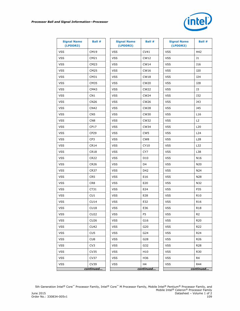
Signal Name(LPDDR3)
Ball #
VSS CM19
VSS CM21
VSS CM23
VSS CM25
VSS CM31
VSS CM35
VSS CM43
VSS CN1
VSS CN26
VSS CN42
VSS CN5
VSS CN8
VSS CP17
VSS CP29
VSS CP3
VSS CR14
VSS CR18
VSS CR22
VSS CR26
VSS CR37
VSS CR5
VSS CR8
VSS CT31
VSS CU1
VSS CU14
VSS CU18
VSS CU22
VSS CU26
VSS CU42
VSS CU5
VSS CU8
VSS CV3
VSS CV35
VSS CV37
VSS CV39
continued...
Signal Name(LPDDR3)
Ball #
VSS CV41
VSS CW12
VSS CW14
VSS CW16
VSS CW18
VSS CW20
VSS CW22
VSS CW24
VSS CW26
VSS CW28
VSS CW30
VSS CW32
VSS CW34
VSS CW5
VSS CW8
VSS CY10
VSS CY7
VSS D10
VSS D4
VSS D42
VSS E16
VSS E20
VSS E24
VSS E28
VSS E32
VSS E36
VSS F5
VSS G16
VSS G20
VSS G24
VSS G28
VSS G32
VSS H10
VSS H36
VSS H4
continued...
Signal Name(LPDDR3)
Ball #
VSS H42
VSS J1
VSS J16
VSS J20
VSS J24
VSS J28
VSS J3
VSS J32
VSS J43
VSS J45
VSS L16
VSS L2
VSS L20
VSS L24
VSS L28
VSS L32
VSS L38
VSS N16
VSS N20
VSS N24
VSS N28
VSS N32
VSS P35
VSS R10
VSS R16
VSS R18
VSS R2
VSS R20
VSS R22
VSS R24
VSS R26
VSS R28
VSS R30
VSS R4
VSS R44
continued...
Processor Ball and Signal Information—Processor
5th Generation Intel® Core™ Processor Family, Intel® Core™ M Processor Family, Mobile Intel® Pentium® Processor Family, andMobile Intel® Celeron® Processor Family
June 2015 Datasheet – Volume 1 of 2Order No.: 330834-005v1 109
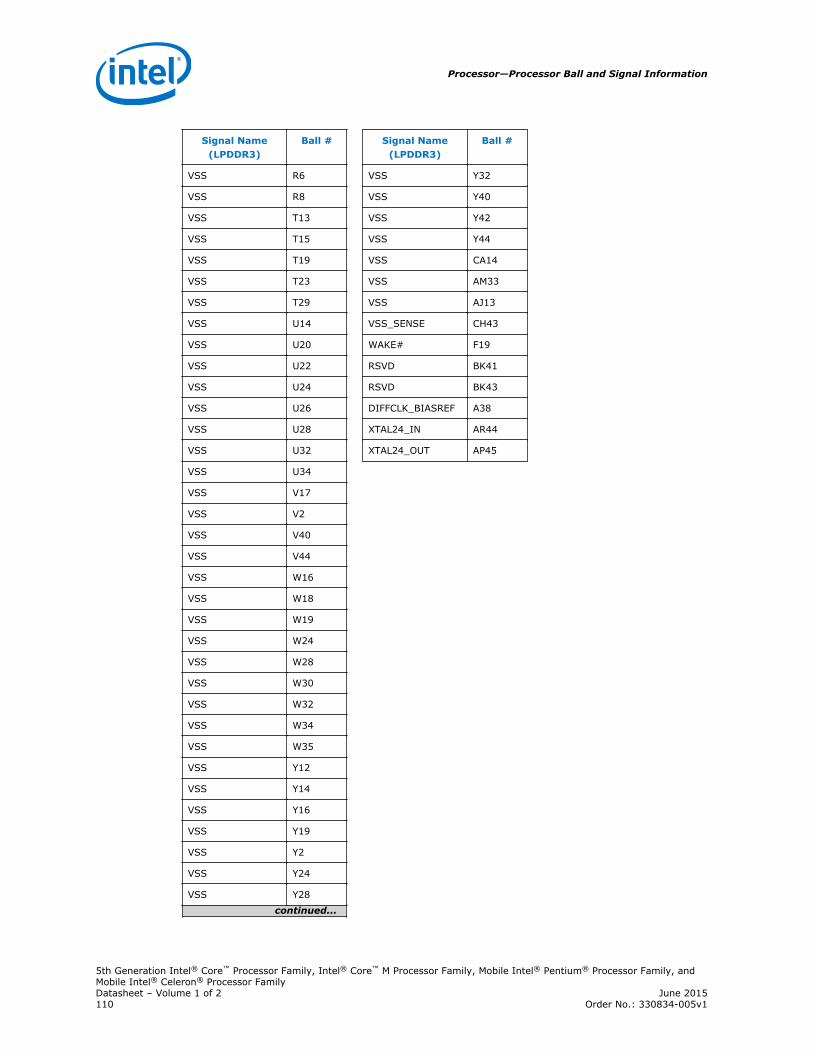
Signal Name(LPDDR3)
Ball #
VSS R6
VSS R8
VSS T13
VSS T15
VSS T19
VSS T23
VSS T29
VSS U14
VSS U20
VSS U22
VSS U24
VSS U26
VSS U28
VSS U32
VSS U34
VSS V17
VSS V2
VSS V40
VSS V44
VSS W16
VSS W18
VSS W19
VSS W24
VSS W28
VSS W30
VSS W32
VSS W34
VSS W35
VSS Y12
VSS Y14
VSS Y16
VSS Y19
VSS Y2
VSS Y24
VSS Y28
continued...
Signal Name(LPDDR3)
Ball #
VSS Y32
VSS Y40
VSS Y42
VSS Y44
VSS CA14
VSS AM33
VSS AJ13
VSS_SENSE CH43
WAKE# F19
RSVD BK41
RSVD BK43
DIFFCLK_BIASREF A38
XTAL24_IN AR44
XTAL24_OUT AP45
Processor—Processor Ball and Signal Information
5th Generation Intel® Core™ Processor Family, Intel® Core™ M Processor Family, Mobile Intel® Pentium® Processor Family, andMobile Intel® Celeron® Processor FamilyDatasheet – Volume 1 of 2 June 2015110 Order No.: 330834-005v1
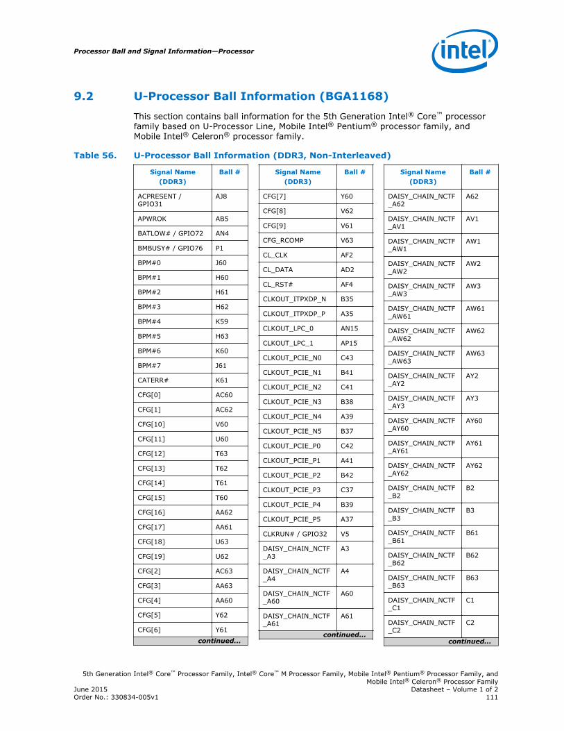
U-Processor Ball Information (BGA1168)
This section contains ball information for the 5th Generation Intel® Core™ processorfamily based on U-Processor Line, Mobile Intel® Pentium® processor family, andMobile Intel® Celeron® processor family.
Table 56. U-Processor Ball Information (DDR3, Non-Interleaved)
Signal Name(DDR3)
Ball #
ACPRESENT /GPIO31
AJ8
APWROK AB5
BATLOW# / GPIO72 AN4
BMBUSY# / GPIO76 P1
BPM#0 J60
BPM#1 H60
BPM#2 H61
BPM#3 H62
BPM#4 K59
BPM#5 H63
BPM#6 K60
BPM#7 J61
CATERR# K61
CFG[0] AC60
CFG[1] AC62
CFG[10] V60
CFG[11] U60
CFG[12] T63
CFG[13] T62
CFG[14] T61
CFG[15] T60
CFG[16] AA62
CFG[17] AA61
CFG[18] U63
CFG[19] U62
CFG[2] AC63
CFG[3] AA63
CFG[4] AA60
CFG[5] Y62
CFG[6] Y61
continued...
Signal Name(DDR3)
Ball #
CFG[7] Y60
CFG[8] V62
CFG[9] V61
CFG_RCOMP V63
CL_CLK AF2
CL_DATA AD2
CL_RST# AF4
CLKOUT_ITPXDP_N B35
CLKOUT_ITPXDP_P A35
CLKOUT_LPC_0 AN15
CLKOUT_LPC_1 AP15
CLKOUT_PCIE_N0 C43
CLKOUT_PCIE_N1 B41
CLKOUT_PCIE_N2 C41
CLKOUT_PCIE_N3 B38
CLKOUT_PCIE_N4 A39
CLKOUT_PCIE_N5 B37
CLKOUT_PCIE_P0 C42
CLKOUT_PCIE_P1 A41
CLKOUT_PCIE_P2 B42
CLKOUT_PCIE_P3 C37
CLKOUT_PCIE_P4 B39
CLKOUT_PCIE_P5 A37
CLKRUN# / GPIO32 V5
DAISY_CHAIN_NCTF_A3
A3
DAISY_CHAIN_NCTF_A4
A4
DAISY_CHAIN_NCTF_A60
A60
DAISY_CHAIN_NCTF_A61
A61
continued...
Signal Name(DDR3)
Ball #
DAISY_CHAIN_NCTF_A62
A62
DAISY_CHAIN_NCTF_AV1
AV1
DAISY_CHAIN_NCTF_AW1
AW1
DAISY_CHAIN_NCTF_AW2
AW2
DAISY_CHAIN_NCTF_AW3
AW3
DAISY_CHAIN_NCTF_AW61
AW61
DAISY_CHAIN_NCTF_AW62
AW62
DAISY_CHAIN_NCTF_AW63
AW63
DAISY_CHAIN_NCTF_AY2
AY2
DAISY_CHAIN_NCTF_AY3
AY3
DAISY_CHAIN_NCTF_AY60
AY60
DAISY_CHAIN_NCTF_AY61
AY61
DAISY_CHAIN_NCTF_AY62
AY62
DAISY_CHAIN_NCTF_B2
B2
DAISY_CHAIN_NCTF_B3
B3
DAISY_CHAIN_NCTF_B61
B61
DAISY_CHAIN_NCTF_B62
B62
DAISY_CHAIN_NCTF_B63
B63
DAISY_CHAIN_NCTF_C1
C1
DAISY_CHAIN_NCTF_C2
C2
continued...
9.2
Processor Ball and Signal Information—Processor
5th Generation Intel® Core™ Processor Family, Intel® Core™ M Processor Family, Mobile Intel® Pentium® Processor Family, andMobile Intel® Celeron® Processor Family
June 2015 Datasheet – Volume 1 of 2Order No.: 330834-005v1 111
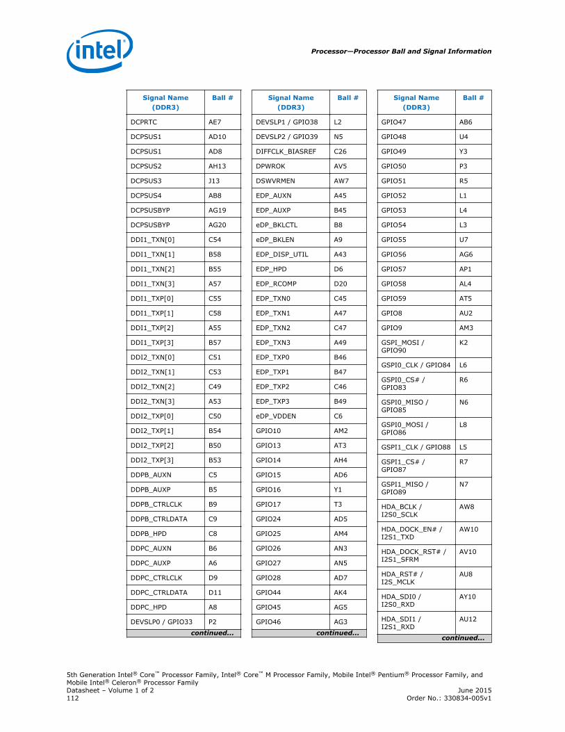
Signal Name(DDR3)
Ball #
DCPRTC AE7
DCPSUS1 AD10
DCPSUS1 AD8
DCPSUS2 AH13
DCPSUS3 J13
DCPSUS4 AB8
DCPSUSBYP AG19
DCPSUSBYP AG20
DDI1_TXN[0] C54
DDI1_TXN[1] B58
DDI1_TXN[2] B55
DDI1_TXN[3] A57
DDI1_TXP[0] C55
DDI1_TXP[1] C58
DDI1_TXP[2] A55
DDI1_TXP[3] B57
DDI2_TXN[0] C51
DDI2_TXN[1] C53
DDI2_TXN[2] C49
DDI2_TXN[3] A53
DDI2_TXP[0] C50
DDI2_TXP[1] B54
DDI2_TXP[2] B50
DDI2_TXP[3] B53
DDPB_AUXN C5
DDPB_AUXP B5
DDPB_CTRLCLK B9
DDPB_CTRLDATA C9
DDPB_HPD C8
DDPC_AUXN B6
DDPC_AUXP A6
DDPC_CTRLCLK D9
DDPC_CTRLDATA D11
DDPC_HPD A8
DEVSLP0 / GPIO33 P2
continued...
Signal Name(DDR3)
Ball #
DEVSLP1 / GPIO38 L2
DEVSLP2 / GPIO39 N5
DIFFCLK_BIASREF C26
DPWROK AV5
DSWVRMEN AW7
EDP_AUXN A45
EDP_AUXP B45
eDP_BKLCTL B8
eDP_BKLEN A9
EDP_DISP_UTIL A43
EDP_HPD D6
EDP_RCOMP D20
EDP_TXN0 C45
EDP_TXN1 A47
EDP_TXN2 C47
EDP_TXN3 A49
EDP_TXP0 B46
EDP_TXP1 B47
EDP_TXP2 C46
EDP_TXP3 B49
eDP_VDDEN C6
GPIO10 AM2
GPIO13 AT3
GPIO14 AH4
GPIO15 AD6
GPIO16 Y1
GPIO17 T3
GPIO24 AD5
GPIO25 AM4
GPIO26 AN3
GPIO27 AN5
GPIO28 AD7
GPIO44 AK4
GPIO45 AG5
GPIO46 AG3
continued...
Signal Name(DDR3)
Ball #
GPIO47 AB6
GPIO48 U4
GPIO49 Y3
GPIO50 P3
GPIO51 R5
GPIO52 L1
GPIO53 L4
GPIO54 L3
GPIO55 U7
GPIO56 AG6
GPIO57 AP1
GPIO58 AL4
GPIO59 AT5
GPIO8 AU2
GPIO9 AM3
GSPI_MOSI /GPIO90
K2
GSPI0_CLK / GPIO84 L6
GSPI0_CS# /GPIO83
R6
GSPI0_MISO /GPIO85
N6
GSPI0_MOSI /GPIO86
L8
GSPI1_CLK / GPIO88 L5
GSPI1_CS# /GPIO87
R7
GSPI1_MISO /GPIO89
N7
HDA_BCLK /I2S0_SCLK
AW8
HDA_DOCK_EN# /I2S1_TXD
AW10
HDA_DOCK_RST# /I2S1_SFRM
AV10
HDA_RST# /I2S_MCLK
AU8
HDA_SDI0 /I2S0_RXD
AY10
HDA_SDI1 /I2S1_RXD
AU12
continued...
Processor—Processor Ball and Signal Information
5th Generation Intel® Core™ Processor Family, Intel® Core™ M Processor Family, Mobile Intel® Pentium® Processor Family, andMobile Intel® Celeron® Processor FamilyDatasheet – Volume 1 of 2 June 2015112 Order No.: 330834-005v1
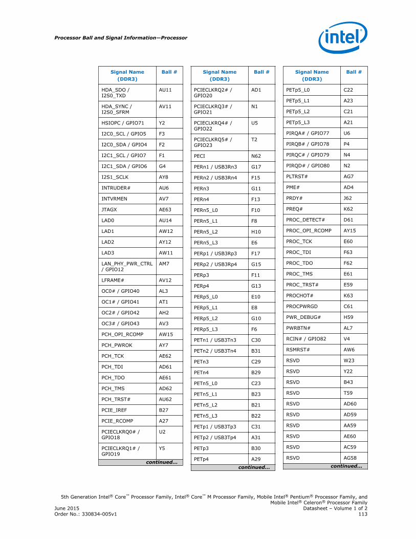
Signal Name(DDR3)
Ball #
HDA_SDO /I2S0_TXD
AU11
HDA_SYNC /I2S0_SFRM
AV11
HSIOPC / GPIO71 Y2
I2C0_SCL / GPIO5 F3
I2C0_SDA / GPIO4 F2
I2C1_SCL / GPIO7 F1
I2C1_SDA / GPIO6 G4
I2S1_SCLK AY8
INTRUDER# AU6
INTVRMEN AV7
JTAGX AE63
LAD0 AU14
LAD1 AW12
LAD2 AY12
LAD3 AW11
LAN_PHY_PWR_CTRL/ GPIO12
AM7
LFRAME# AV12
OC0# / GPIO40 AL3
OC1# / GPIO41 AT1
OC2# / GPIO42 AH2
OC3# / GPIO43 AV3
PCH_OPI_RCOMP AW15
PCH_PWROK AY7
PCH_TCK AE62
PCH_TDI AD61
PCH_TDO AE61
PCH_TMS AD62
PCH_TRST# AU62
PCIE_IREF B27
PCIE_RCOMP A27
PCIECLKRQ0# /GPIO18
U2
PCIECLKRQ1# /GPIO19
Y5
continued...
Signal Name(DDR3)
Ball #
PCIECLKRQ2# /GPIO20
AD1
PCIECLKRQ3# /GPIO21
N1
PCIECLKRQ4# /GPIO22
U5
PCIECLKRQ5# /GPIO23
T2
PECI N62
PERn1 / USB3Rn3 G17
PERn2 / USB3Rn4 F15
PERn3 G11
PERn4 F13
PERn5_L0 F10
PERn5_L1 F8
PERn5_L2 H10
PERn5_L3 E6
PERp1 / USB3Rp3 F17
PERp2 / USB3Rp4 G15
PERp3 F11
PERp4 G13
PERp5_L0 E10
PERp5_L1 E8
PERp5_L2 G10
PERp5_L3 F6
PETn1 / USB3Tn3 C30
PETn2 / USB3Tn4 B31
PETn3 C29
PETn4 B29
PETn5_L0 C23
PETn5_L1 B23
PETn5_L2 B21
PETn5_L3 B22
PETp1 / USB3Tp3 C31
PETp2 / USB3Tp4 A31
PETp3 B30
PETp4 A29
continued...
Signal Name(DDR3)
Ball #
PETp5_L0 C22
PETp5_L1 A23
PETp5_L2 C21
PETp5_L3 A21
PIRQA# / GPIO77 U6
PIRQB# / GPIO78 P4
PIRQC# / GPIO79 N4
PIRQD# / GPIO80 N2
PLTRST# AG7
PME# AD4
PRDY# J62
PREQ# K62
PROC_DETECT# D61
PROC_OPI_RCOMP AY15
PROC_TCK E60
PROC_TDI F63
PROC_TDO F62
PROC_TMS E61
PROC_TRST# E59
PROCHOT# K63
PROCPWRGD C61
PWR_DEBUG# H59
PWRBTN# AL7
RCIN# / GPIO82 V4
RSMRST# AW6
RSVD W23
RSVD Y22
RSVD B43
RSVD T59
RSVD AD60
RSVD AD59
RSVD AA59
RSVD AE60
RSVD AC59
RSVD AG58
continued...
Processor Ball and Signal Information—Processor
5th Generation Intel® Core™ Processor Family, Intel® Core™ M Processor Family, Mobile Intel® Pentium® Processor Family, andMobile Intel® Celeron® Processor Family
June 2015 Datasheet – Volume 1 of 2Order No.: 330834-005v1 113
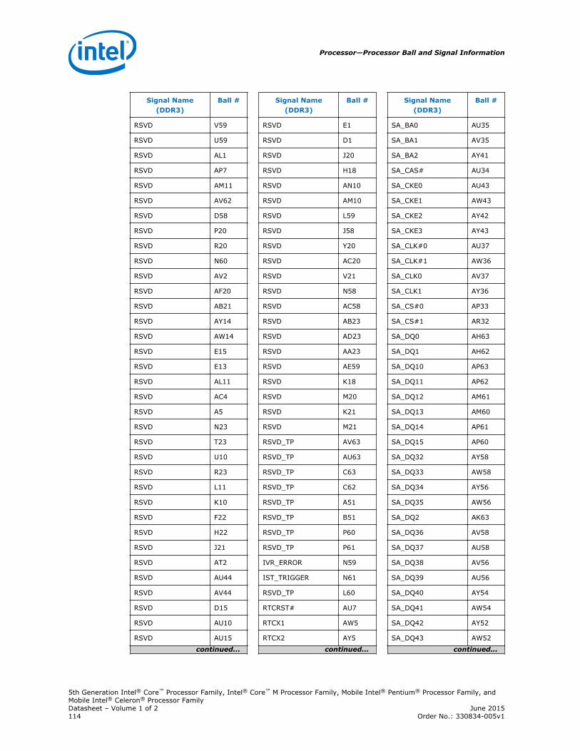
Signal Name(DDR3)
Ball #
RSVD V59
RSVD U59
RSVD AL1
RSVD AP7
RSVD AM11
RSVD AV62
RSVD D58
RSVD P20
RSVD R20
RSVD N60
RSVD AV2
RSVD AF20
RSVD AB21
RSVD AY14
RSVD AW14
RSVD E15
RSVD E13
RSVD AL11
RSVD AC4
RSVD A5
RSVD N23
RSVD T23
RSVD U10
RSVD R23
RSVD L11
RSVD K10
RSVD F22
RSVD H22
RSVD J21
RSVD AT2
RSVD AU44
RSVD AV44
RSVD D15
RSVD AU10
RSVD AU15
continued...
Signal Name(DDR3)
Ball #
RSVD E1
RSVD D1
RSVD J20
RSVD H18
RSVD AN10
RSVD AM10
RSVD L59
RSVD J58
RSVD Y20
RSVD AC20
RSVD V21
RSVD N58
RSVD AC58
RSVD AB23
RSVD AD23
RSVD AA23
RSVD AE59
RSVD K18
RSVD M20
RSVD K21
RSVD M21
RSVD_TP AV63
RSVD_TP AU63
RSVD_TP C63
RSVD_TP C62
RSVD_TP A51
RSVD_TP B51
RSVD_TP P60
RSVD_TP P61
IVR_ERROR N59
IST_TRIGGER N61
RSVD_TP L60
RTCRST# AU7
RTCX1 AW5
RTCX2 AY5
continued...
Signal Name(DDR3)
Ball #
SA_BA0 AU35
SA_BA1 AV35
SA_BA2 AY41
SA_CAS# AU34
SA_CKE0 AU43
SA_CKE1 AW43
SA_CKE2 AY42
SA_CKE3 AY43
SA_CLK#0 AU37
SA_CLK#1 AW36
SA_CLK0 AV37
SA_CLK1 AY36
SA_CS#0 AP33
SA_CS#1 AR32
SA_DQ0 AH63
SA_DQ1 AH62
SA_DQ10 AP63
SA_DQ11 AP62
SA_DQ12 AM61
SA_DQ13 AM60
SA_DQ14 AP61
SA_DQ15 AP60
SA_DQ32 AY58
SA_DQ33 AW58
SA_DQ34 AY56
SA_DQ35 AW56
SA_DQ2 AK63
SA_DQ36 AV58
SA_DQ37 AU58
SA_DQ38 AV56
SA_DQ39 AU56
SA_DQ40 AY54
SA_DQ41 AW54
SA_DQ42 AY52
SA_DQ43 AW52
continued...
Processor—Processor Ball and Signal Information
5th Generation Intel® Core™ Processor Family, Intel® Core™ M Processor Family, Mobile Intel® Pentium® Processor Family, andMobile Intel® Celeron® Processor FamilyDatasheet – Volume 1 of 2 June 2015114 Order No.: 330834-005v1
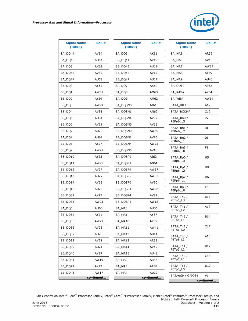
Signal Name(DDR3)
Ball #
SA_DQ44 AV54
SA_DQ45 AU54
SA_DQ3 AK62
SA_DQ46 AV52
SA_DQ47 AU52
SB_DQ0 AY31
SB_DQ1 AW31
SB_DQ2 AY29
SB_DQ3 AW29
SB_DQ4 AV31
SB_DQ5 AU31
SB_DQ6 AV29
SB_DQ7 AU29
SA_DQ4 AH61
SB_DQ8 AY27
SB_DQ9 AW27
SB_DQ10 AY25
SB_DQ11 AW25
SB_DQ12 AV27
SB_DQ13 AU27
SB_DQ14 AV25
SB_DQ15 AU25
SB_DQ32 AY23
SB_DQ33 AW23
SA_DQ5 AH60
SB_DQ34 AY21
SB_DQ35 AW21
SB_DQ36 AV23
SB_DQ37 AU23
SB_DQ38 AV21
SB_DQ39 AU21
SB_DQ40 AY19
SB_DQ41 AW19
SB_DQ42 AY17
SB_DQ43 AW17
continued...
Signal Name(DDR3)
Ball #
SA_DQ6 AK61
SB_DQ44 AV19
SB_DQ45 AU19
SB_DQ46 AV17
SB_DQ47 AU17
SA_DQ7 AK60
SA_DQ8 AM63
SA_DQ9 AM62
SA_DQSN0 AJ61
SA_DQSN1 AN62
SA_DQSN4 AV57
SA_DQSN5 AV53
SB_DQSN0 AW30
SB_DQSN1 AV26
SB_DQSN4 AW22
SB_DQSN5 AV18
SA_DQSP0 AJ62
SA_DQSP1 AN61
SA_DQSP4 AW57
SA_DQSP5 AW53
SB_DQSP0 AV30
SB_DQSP1 AW26
SB_DQSP4 AV22
SB_DQSP5 AW18
SA_MA0 AU36
SA_MA1 AY37
SA_MA10 AP35
SA_MA11 AW41
SA_MA12 AU41
SA_MA13 AR35
SA_MA14 AV42
SA_MA15 AU42
SA_MA2 AR38
SA_MA3 AP36
SA_MA4 AU39
continued...
Signal Name(DDR3)
Ball #
SA_MA5 AR36
SA_MA6 AV40
SA_MA7 AW39
SA_MA8 AY39
SA_MA9 AU40
SA_ODT0 AP32
SA_RAS# AY34
SA_WE# AW34
SATA_IREF A12
SATA_RCOMP C12
SATA_Rn0 /PERn6_L3
J5
SATA_Rn1 /PERn6_L2
J8
SATA_Rn2 /PERn6_L1
J6
SATA_Rn3 /PERn6_L0
F5
SATA_Rp0 /PERp6_L3
H5
SATA_Rp1 /PERp6_L2
H8
SATA_Rp2 /PERp6_L1
H6
SATA_Rp3 /PERp6_L0
E5
SATA_Tn0 /PETn6_L3
B15
SATA_Tn1 /PETn6_L2
A17
SATA_Tn2 /PETn6_L1
B14
SATA_Tn3 /PETn6_L0
C17
SATA_Tp0 /PETp6_L3
A15
SATA_Tp1 /PETp6_L2
B17
SATA_Tp2 /PETp6_L1
C15
SATA_Tp3 /PETp6_L0
D17
SATA0GP / GPIO34 V1
continued...
Processor Ball and Signal Information—Processor
5th Generation Intel® Core™ Processor Family, Intel® Core™ M Processor Family, Mobile Intel® Pentium® Processor Family, andMobile Intel® Celeron® Processor Family
June 2015 Datasheet – Volume 1 of 2Order No.: 330834-005v1 115
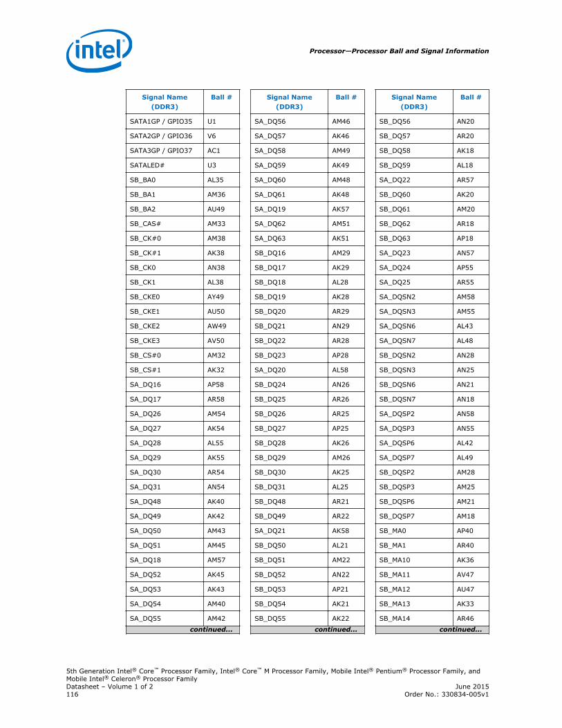
Signal Name(DDR3)
Ball #
SATA1GP / GPIO35 U1
SATA2GP / GPIO36 V6
SATA3GP / GPIO37 AC1
SATALED# U3
SB_BA0 AL35
SB_BA1 AM36
SB_BA2 AU49
SB_CAS# AM33
SB_CK#0 AM38
SB_CK#1 AK38
SB_CK0 AN38
SB_CK1 AL38
SB_CKE0 AY49
SB_CKE1 AU50
SB_CKE2 AW49
SB_CKE3 AV50
SB_CS#0 AM32
SB_CS#1 AK32
SA_DQ16 AP58
SA_DQ17 AR58
SA_DQ26 AM54
SA_DQ27 AK54
SA_DQ28 AL55
SA_DQ29 AK55
SA_DQ30 AR54
SA_DQ31 AN54
SA_DQ48 AK40
SA_DQ49 AK42
SA_DQ50 AM43
SA_DQ51 AM45
SA_DQ18 AM57
SA_DQ52 AK45
SA_DQ53 AK43
SA_DQ54 AM40
SA_DQ55 AM42
continued...
Signal Name(DDR3)
Ball #
SA_DQ56 AM46
SA_DQ57 AK46
SA_DQ58 AM49
SA_DQ59 AK49
SA_DQ60 AM48
SA_DQ61 AK48
SA_DQ19 AK57
SA_DQ62 AM51
SA_DQ63 AK51
SB_DQ16 AM29
SB_DQ17 AK29
SB_DQ18 AL28
SB_DQ19 AK28
SB_DQ20 AR29
SB_DQ21 AN29
SB_DQ22 AR28
SB_DQ23 AP28
SA_DQ20 AL58
SB_DQ24 AN26
SB_DQ25 AR26
SB_DQ26 AR25
SB_DQ27 AP25
SB_DQ28 AK26
SB_DQ29 AM26
SB_DQ30 AK25
SB_DQ31 AL25
SB_DQ48 AR21
SB_DQ49 AR22
SA_DQ21 AK58
SB_DQ50 AL21
SB_DQ51 AM22
SB_DQ52 AN22
SB_DQ53 AP21
SB_DQ54 AK21
SB_DQ55 AK22
continued...
Signal Name(DDR3)
Ball #
SB_DQ56 AN20
SB_DQ57 AR20
SB_DQ58 AK18
SB_DQ59 AL18
SA_DQ22 AR57
SB_DQ60 AK20
SB_DQ61 AM20
SB_DQ62 AR18
SB_DQ63 AP18
SA_DQ23 AN57
SA_DQ24 AP55
SA_DQ25 AR55
SA_DQSN2 AM58
SA_DQSN3 AM55
SA_DQSN6 AL43
SA_DQSN7 AL48
SB_DQSN2 AN28
SB_DQSN3 AN25
SB_DQSN6 AN21
SB_DQSN7 AN18
SA_DQSP2 AN58
SA_DQSP3 AN55
SA_DQSP6 AL42
SA_DQSP7 AL49
SB_DQSP2 AM28
SB_DQSP3 AM25
SB_DQSP6 AM21
SB_DQSP7 AM18
SB_MA0 AP40
SB_MA1 AR40
SB_MA10 AK36
SB_MA11 AV47
SB_MA12 AU47
SB_MA13 AK33
SB_MA14 AR46
continued...
Processor—Processor Ball and Signal Information
5th Generation Intel® Core™ Processor Family, Intel® Core™ M Processor Family, Mobile Intel® Pentium® Processor Family, andMobile Intel® Celeron® Processor FamilyDatasheet – Volume 1 of 2 June 2015116 Order No.: 330834-005v1
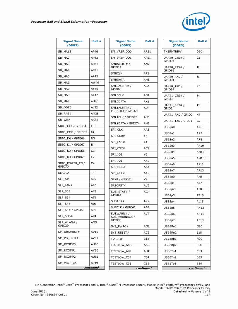
Signal Name(DDR3)
Ball #
SB_MA15 AP46
SB_MA2 AP42
SB_MA3 AR42
SB_MA4 AR45
SB_MA5 AP45
SB_MA6 AW46
SB_MA7 AY46
SB_MA8 AY47
SB_MA9 AU46
SB_ODT0 AL32
SB_RAS# AM35
SB_WE# AK35
SDIO_CLK / GPIO64 E3
SDIO_CMD / GPIO65 F4
SDIO_D0 / GPIO66 D3
SDIO_D1 / GPIO67 E4
SDIO_D2 / GPIO68 C3
SDIO_D3 / GPIO69 E2
SDIO_POWER_EN /GPIO70
C4
SERIRQ T4
SLP_A# AL5
SLP_LAN# AJ7
SLP_S0# AF3
SLP_S3# AT4
SLP_S4# AJ6
SLP_S5# / GPIO63 AP5
SLP_SUS# AP4
SLP_WLAN# /GPIO29
AM5
SM_DRAMRST# AV15
SM_PG_CNTL1 AV61
SM_RCOMP0 AU60
SM_RCOMP1 AV60
SM_RCOMP2 AU61
SM_VREF_CA AP49
continued...
Signal Name(DDR3)
Ball #
SM_VREF_DQ0 AR51
SM_VREF_DQ1 AP51
SMBALERT# /GPIO11
AN2
SMBCLK AP2
SMBDATA AH1
SML0ALERT# /GPIO60
AL2
SML0CLK AN1
SML0DATA AK1
SML1ALERT# /PCHHOT# / GPIO73
AU4
SML1CLK / GPIO75 AU3
SML1DATA / GPIO74 AH3
SPI_CLK AA3
SPI_CS0# Y7
SPI_CS1# Y4
SPI_CS2# AC2
SPI_IO2 Y6
SPI_IO3 AF1
SPI_MISO AA4
SPI_MOSI AA2
SPKR / GPIO81 V2
SRTCRST# AV6
SUS_STAT# /GPIO61
AG4
SUSACK# AK2
SUSCLK / GPIO62 AE6
SUSWARN# /SUSPWRDNACK /GPIO30
AV4
SYS_PWROK AG2
SYS_RESET# AC3
TD_IREF B12
TESTLOW_AK8 AK8
TESTLOW_AL8 AL8
TESTLOW_C34 C34
TESTLOW_C35 C35
continued...
Signal Name(DDR3)
Ball #
THERMTRIP# D60
UART0_CTS# /GPIO94
G1
UART0_RTS# /GPIO93
J2
UART0_RXD /GPIO91
J1
UART0_TXD /GPIO92
K3
UART1_CTS# /GPIO3
J4
UART1_RST# /GPIO2
J3
UART1_RXD / GPIO0 K4
UART1_TXD / GPIO1 G2
USB2n0 AN8
USB2n1 AR7
USB2n2 AR8
USB2n3 AR10
USB2n4 AM15
USB2n5 AM13
USB2n6 AP11
USB2n7 AR13
USB2p0 AM8
USB2p1 AT7
USB2p2 AP8
USB2p3 AT10
USB2p4 AL15
USB2p5 AN13
USB2p6 AN11
USB2p7 AP13
USB3Rn1 G20
USB3Rn2 E18
USB3Rp1 H20
USB3Rp2 F18
USB3Tn1 C33
USB3Tn2 B33
USB3Tp1 B34
continued...
Processor Ball and Signal Information—Processor
5th Generation Intel® Core™ Processor Family, Intel® Core™ M Processor Family, Mobile Intel® Pentium® Processor Family, andMobile Intel® Celeron® Processor Family
June 2015 Datasheet – Volume 1 of 2Order No.: 330834-005v1 117

Signal Name(DDR3)
Ball #
USB3Tp2 A33
USBRBIAS AJ11
USBRBIAS# AJ10
VCC F59
VCC AB57
VCC AD57
VCC AG57
VCC C24
VCC C28
VCC C32
VCC C36
VCC C40
VCC C44
VCC C48
VCC C52
VCC C56
VCC E23
VCC E25
VCC E27
VCC E29
VCC E31
VCC E33
VCC E35
VCC E37
VCC E39
VCC E41
VCC E43
VCC E45
VCC E47
VCC E49
VCC E51
VCC E53
VCC E55
VCC E57
VCC F24
continued...
Signal Name(DDR3)
Ball #
VCC F28
VCC F32
VCC F36
VCC F40
VCC F44
VCC F48
VCC F52
VCC F56
VCC G23
VCC G25
VCC G27
VCC G29
VCC G31
VCC G33
VCC G35
VCC G37
VCC G39
VCC G41
VCC G43
VCC G45
VCC G47
VCC G49
VCC G51
VCC G53
VCC G55
VCC G57
VCC H23
VCC J23
VCC K23
VCC K57
VCC L22
VCC M23
VCC M57
VCC P57
VCC U57
continued...
Signal Name(DDR3)
Ball #
VCC W57
VCC_SENSE E63
VCC1_05 P9
VCC1_05 N8
VCC1_05 AE8
VCC1_05 AF22
VCC1_05 H11
VCC1_05 H15
VCC1_05 J11
VCC1_05 AG16
VCC1_05 AG17
VCC3_3 V8
VCC3_3 W9
VCC3_3 K14
VCC3_3 K16
VCCACLKPLL A20
VCCAPLL AA21
VCCAPLL W21
VCCASW AE9
VCCASW AF9
VCCASW AG8
VCCASW AG13
VCCASW AG14
VCCCLK J18
VCCCLK K19
VCCCLK J17
VCCCLK T21
VCCCLK R21
VCCDSW3_3 AH10
VCCHDA AH14
VCCHSIO M9
VCCHSIO K9
VCCHSIO L10
VCCIO_OUT A59
VCOMP_OUT E20
continued...
Processor—Processor Ball and Signal Information
5th Generation Intel® Core™ Processor Family, Intel® Core™ M Processor Family, Mobile Intel® Pentium® Processor Family, andMobile Intel® Celeron® Processor FamilyDatasheet – Volume 1 of 2 June 2015118 Order No.: 330834-005v1
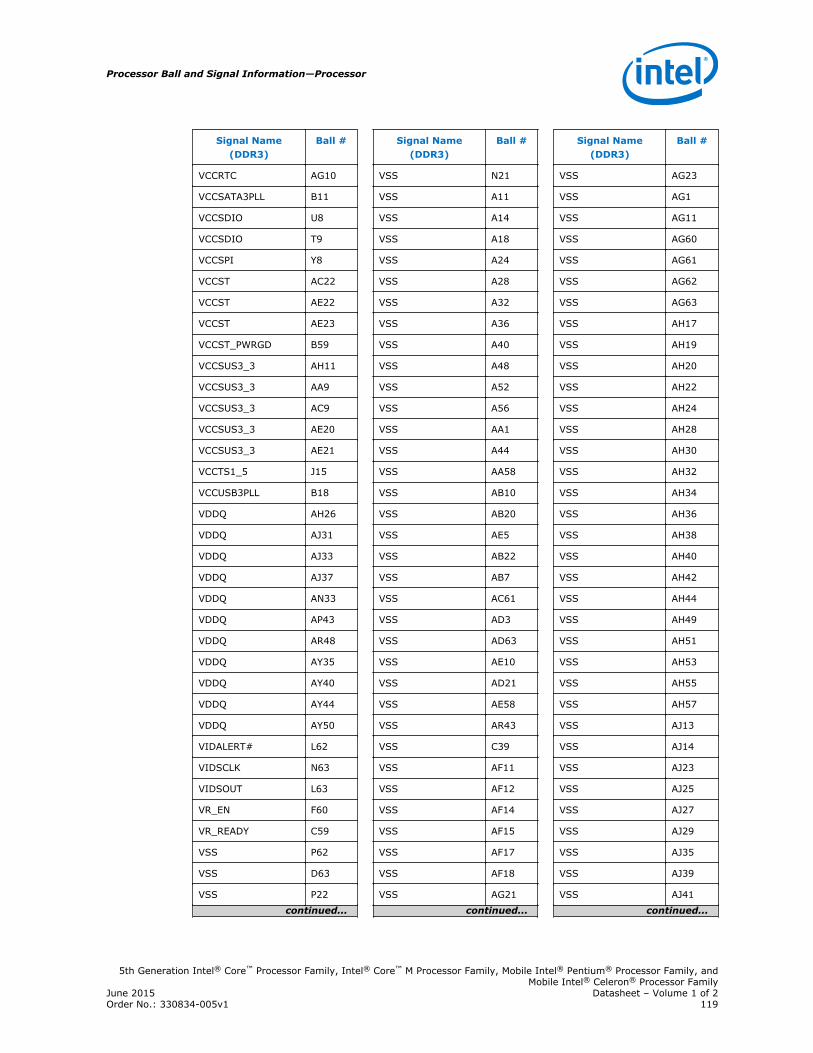
Signal Name(DDR3)
Ball #
VCCRTC AG10
VCCSATA3PLL B11
VCCSDIO U8
VCCSDIO T9
VCCSPI Y8
VCCST AC22
VCCST AE22
VCCST AE23
VCCST_PWRGD B59
VCCSUS3_3 AH11
VCCSUS3_3 AA9
VCCSUS3_3 AC9
VCCSUS3_3 AE20
VCCSUS3_3 AE21
VCCTS1_5 J15
VCCUSB3PLL B18
VDDQ AH26
VDDQ AJ31
VDDQ AJ33
VDDQ AJ37
VDDQ AN33
VDDQ AP43
VDDQ AR48
VDDQ AY35
VDDQ AY40
VDDQ AY44
VDDQ AY50
VIDALERT# L62
VIDSCLK N63
VIDSOUT L63
VR_EN F60
VR_READY C59
VSS P62
VSS D63
VSS P22
continued...
Signal Name(DDR3)
Ball #
VSS N21
VSS A11
VSS A14
VSS A18
VSS A24
VSS A28
VSS A32
VSS A36
VSS A40
VSS A48
VSS A52
VSS A56
VSS AA1
VSS A44
VSS AA58
VSS AB10
VSS AB20
VSS AE5
VSS AB22
VSS AB7
VSS AC61
VSS AD3
VSS AD63
VSS AE10
VSS AD21
VSS AE58
VSS AR43
VSS C39
VSS AF11
VSS AF12
VSS AF14
VSS AF15
VSS AF17
VSS AF18
VSS AG21
continued...
Signal Name(DDR3)
Ball #
VSS AG23
VSS AG1
VSS AG11
VSS AG60
VSS AG61
VSS AG62
VSS AG63
VSS AH17
VSS AH19
VSS AH20
VSS AH22
VSS AH24
VSS AH28
VSS AH30
VSS AH32
VSS AH34
VSS AH36
VSS AH38
VSS AH40
VSS AH42
VSS AH44
VSS AH49
VSS AH51
VSS AH53
VSS AH55
VSS AH57
VSS AJ13
VSS AJ14
VSS AJ23
VSS AJ25
VSS AJ27
VSS AJ29
VSS AJ35
VSS AJ39
VSS AJ41
continued...
Processor Ball and Signal Information—Processor
5th Generation Intel® Core™ Processor Family, Intel® Core™ M Processor Family, Mobile Intel® Pentium® Processor Family, andMobile Intel® Celeron® Processor Family
June 2015 Datasheet – Volume 1 of 2Order No.: 330834-005v1 119
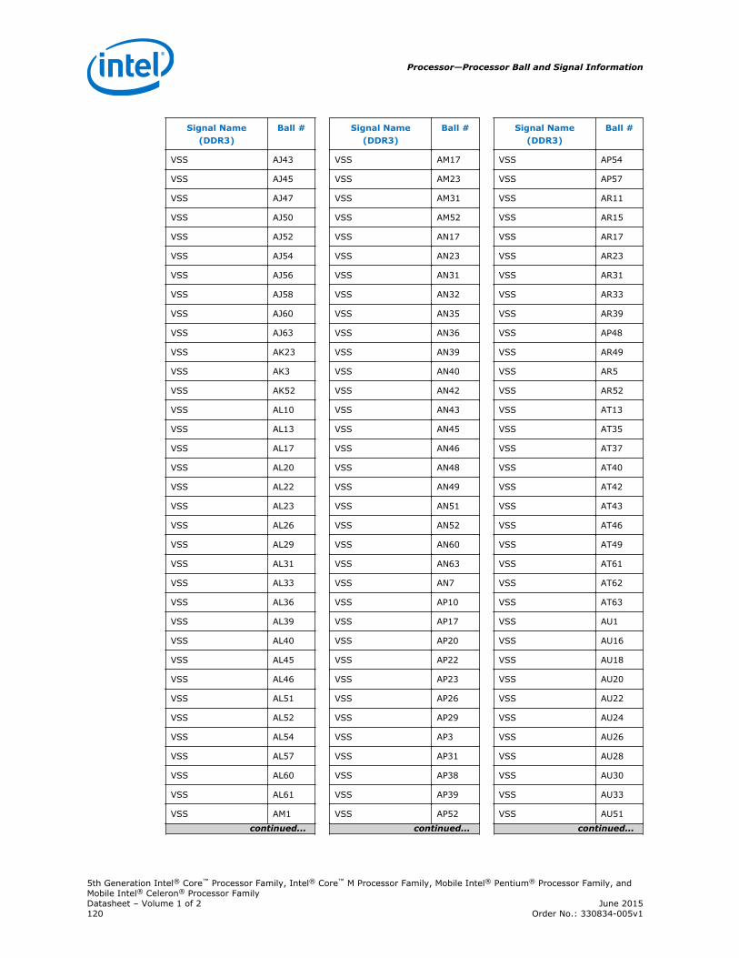
Signal Name(DDR3)
Ball #
VSS AJ43
VSS AJ45
VSS AJ47
VSS AJ50
VSS AJ52
VSS AJ54
VSS AJ56
VSS AJ58
VSS AJ60
VSS AJ63
VSS AK23
VSS AK3
VSS AK52
VSS AL10
VSS AL13
VSS AL17
VSS AL20
VSS AL22
VSS AL23
VSS AL26
VSS AL29
VSS AL31
VSS AL33
VSS AL36
VSS AL39
VSS AL40
VSS AL45
VSS AL46
VSS AL51
VSS AL52
VSS AL54
VSS AL57
VSS AL60
VSS AL61
VSS AM1
continued...
Signal Name(DDR3)
Ball #
VSS AM17
VSS AM23
VSS AM31
VSS AM52
VSS AN17
VSS AN23
VSS AN31
VSS AN32
VSS AN35
VSS AN36
VSS AN39
VSS AN40
VSS AN42
VSS AN43
VSS AN45
VSS AN46
VSS AN48
VSS AN49
VSS AN51
VSS AN52
VSS AN60
VSS AN63
VSS AN7
VSS AP10
VSS AP17
VSS AP20
VSS AP22
VSS AP23
VSS AP26
VSS AP29
VSS AP3
VSS AP31
VSS AP38
VSS AP39
VSS AP52
continued...
Signal Name(DDR3)
Ball #
VSS AP54
VSS AP57
VSS AR11
VSS AR15
VSS AR17
VSS AR23
VSS AR31
VSS AR33
VSS AR39
VSS AP48
VSS AR49
VSS AR5
VSS AR52
VSS AT13
VSS AT35
VSS AT37
VSS AT40
VSS AT42
VSS AT43
VSS AT46
VSS AT49
VSS AT61
VSS AT62
VSS AT63
VSS AU1
VSS AU16
VSS AU18
VSS AU20
VSS AU22
VSS AU24
VSS AU26
VSS AU28
VSS AU30
VSS AU33
VSS AU51
continued...
Processor—Processor Ball and Signal Information
5th Generation Intel® Core™ Processor Family, Intel® Core™ M Processor Family, Mobile Intel® Pentium® Processor Family, andMobile Intel® Celeron® Processor FamilyDatasheet – Volume 1 of 2 June 2015120 Order No.: 330834-005v1
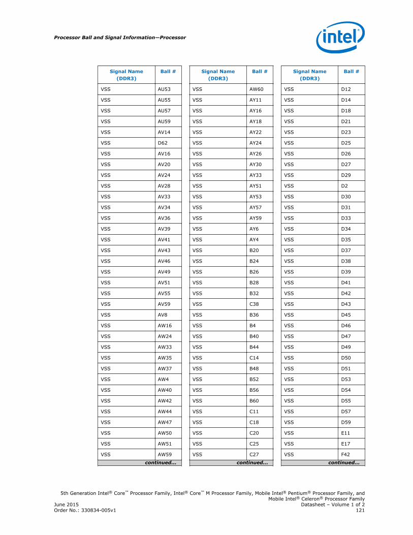
Signal Name(DDR3)
Ball #
VSS AU53
VSS AU55
VSS AU57
VSS AU59
VSS AV14
VSS D62
VSS AV16
VSS AV20
VSS AV24
VSS AV28
VSS AV33
VSS AV34
VSS AV36
VSS AV39
VSS AV41
VSS AV43
VSS AV46
VSS AV49
VSS AV51
VSS AV55
VSS AV59
VSS AV8
VSS AW16
VSS AW24
VSS AW33
VSS AW35
VSS AW37
VSS AW4
VSS AW40
VSS AW42
VSS AW44
VSS AW47
VSS AW50
VSS AW51
VSS AW59
continued...
Signal Name(DDR3)
Ball #
VSS AW60
VSS AY11
VSS AY16
VSS AY18
VSS AY22
VSS AY24
VSS AY26
VSS AY30
VSS AY33
VSS AY51
VSS AY53
VSS AY57
VSS AY59
VSS AY6
VSS AY4
VSS B20
VSS B24
VSS B26
VSS B28
VSS B32
VSS C38
VSS B36
VSS B4
VSS B40
VSS B44
VSS C14
VSS B48
VSS B52
VSS B56
VSS B60
VSS C11
VSS C18
VSS C20
VSS C25
VSS C27
continued...
Signal Name(DDR3)
Ball #
VSS D12
VSS D14
VSS D18
VSS D21
VSS D23
VSS D25
VSS D26
VSS D27
VSS D29
VSS D2
VSS D30
VSS D31
VSS D33
VSS D34
VSS D35
VSS D37
VSS D38
VSS D39
VSS D41
VSS D42
VSS D43
VSS D45
VSS D46
VSS D47
VSS D49
VSS D50
VSS D51
VSS D53
VSS D54
VSS D55
VSS D57
VSS D59
VSS E11
VSS E17
VSS F42
continued...
Processor Ball and Signal Information—Processor
5th Generation Intel® Core™ Processor Family, Intel® Core™ M Processor Family, Mobile Intel® Pentium® Processor Family, andMobile Intel® Celeron® Processor Family
June 2015 Datasheet – Volume 1 of 2Order No.: 330834-005v1 121
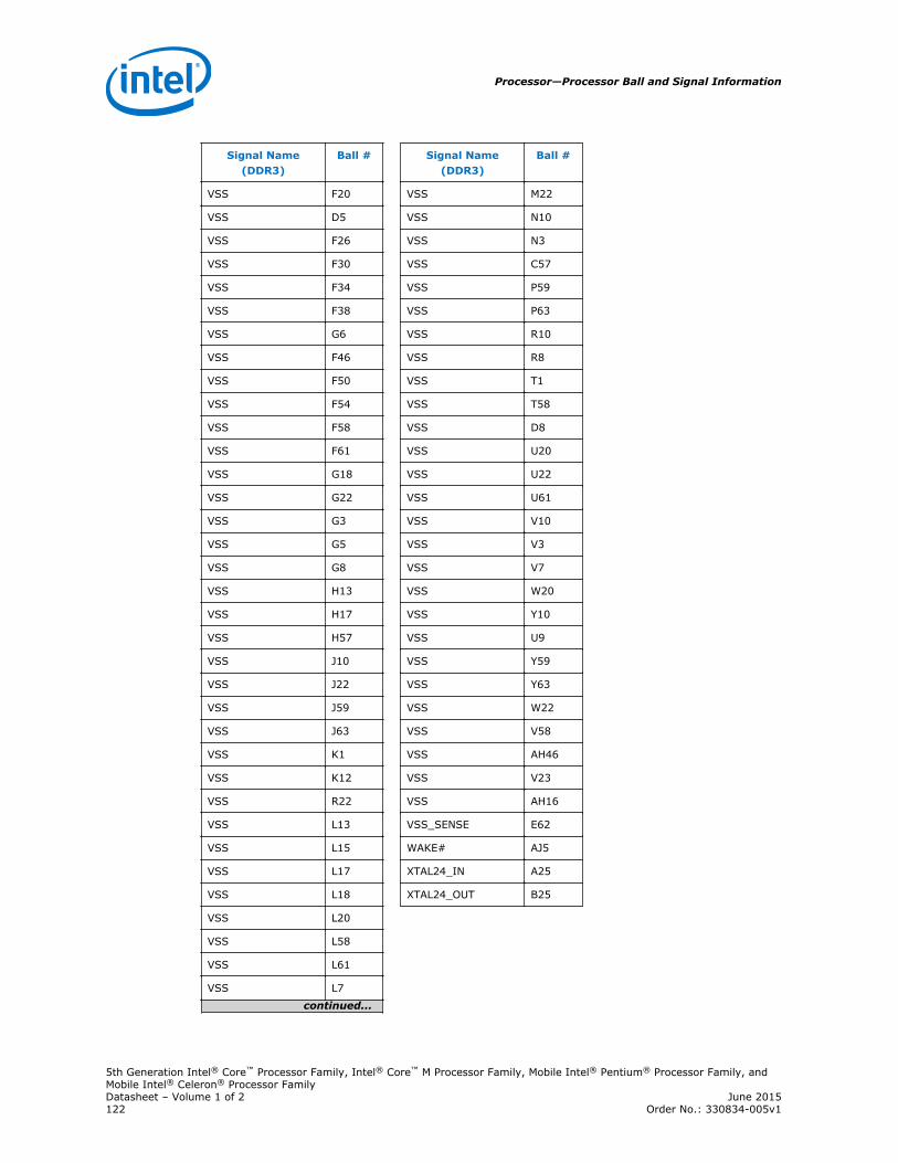
Signal Name(DDR3)
Ball #
VSS F20
VSS D5
VSS F26
VSS F30
VSS F34
VSS F38
VSS G6
VSS F46
VSS F50
VSS F54
VSS F58
VSS F61
VSS G18
VSS G22
VSS G3
VSS G5
VSS G8
VSS H13
VSS H17
VSS H57
VSS J10
VSS J22
VSS J59
VSS J63
VSS K1
VSS K12
VSS R22
VSS L13
VSS L15
VSS L17
VSS L18
VSS L20
VSS L58
VSS L61
VSS L7
continued...
Signal Name(DDR3)
Ball #
VSS M22
VSS N10
VSS N3
VSS C57
VSS P59
VSS P63
VSS R10
VSS R8
VSS T1
VSS T58
VSS D8
VSS U20
VSS U22
VSS U61
VSS V10
VSS V3
VSS V7
VSS W20
VSS Y10
VSS U9
VSS Y59
VSS Y63
VSS W22
VSS V58
VSS AH46
VSS V23
VSS AH16
VSS_SENSE E62
WAKE# AJ5
XTAL24_IN A25
XTAL24_OUT B25
Processor—Processor Ball and Signal Information
5th Generation Intel® Core™ Processor Family, Intel® Core™ M Processor Family, Mobile Intel® Pentium® Processor Family, andMobile Intel® Celeron® Processor FamilyDatasheet – Volume 1 of 2 June 2015122 Order No.: 330834-005v1
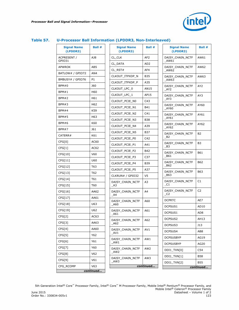
Table 57. U-Processor Ball Information (LPDDR3, Non-Interleaved)
Signal Name(LPDDR3)
Ball #
ACPRESENT /GPIO31
AJ8
APWROK AB5
BATLOW# / GPIO72 AN4
BMBUSY# / GPIO76 P1
BPM#0 J60
BPM#1 H60
BPM#2 H61
BPM#3 H62
BPM#4 K59
BPM#5 H63
BPM#6 K60
BPM#7 J61
CATERR# K61
CFG[0] AC60
CFG[1] AC62
CFG[10] V60
CFG[11] U60
CFG[12] T63
CFG[13] T62
CFG[14] T61
CFG[15] T60
CFG[16] AA62
CFG[17] AA61
CFG[18] U63
CFG[19] U62
CFG[2] AC63
CFG[3] AA63
CFG[4] AA60
CFG[5] Y62
CFG[6] Y61
CFG[7] Y60
CFG[8] V62
CFG[9] V61
CFG_RCOMP V63
continued...
Signal Name(LPDDR3)
Ball #
CL_CLK AF2
CL_DATA AD2
CL_RST# AF4
CLKOUT_ITPXDP_N B35
CLKOUT_ITPXDP_P A35
CLKOUT_LPC_0 AN15
CLKOUT_LPC_1 AP15
CLKOUT_PCIE_N0 C43
CLKOUT_PCIE_N1 B41
CLKOUT_PCIE_N2 C41
CLKOUT_PCIE_N3 B38
CLKOUT_PCIE_N4 A39
CLKOUT_PCIE_N5 B37
CLKOUT_PCIE_P0 C42
CLKOUT_PCIE_P1 A41
CLKOUT_PCIE_P2 B42
CLKOUT_PCIE_P3 C37
CLKOUT_PCIE_P4 B39
CLKOUT_PCIE_P5 A37
CLKRUN# / GPIO32 V5
DAISY_CHAIN_NCTF_A3
A3
DAISY_CHAIN_NCTF_A4
A4
DAISY_CHAIN_NCTF_A60
A60
DAISY_CHAIN_NCTF_A61
A61
DAISY_CHAIN_NCTF_A62
A62
DAISY_CHAIN_NCTF_AV1
AV1
DAISY_CHAIN_NCTF_AW1
AW1
DAISY_CHAIN_NCTF_AW2
AW2
DAISY_CHAIN_NCTF_AW3
AW3
continued...
Signal Name(LPDDR3)
Ball #
DAISY_CHAIN_NCTF_AW61
AW61
DAISY_CHAIN_NCTF_AW62
AW62
DAISY_CHAIN_NCTF_AW63
AW63
DAISY_CHAIN_NCTF_AY2
AY2
DAISY_CHAIN_NCTF_AY3
AY3
DAISY_CHAIN_NCTF_AY60
AY60
DAISY_CHAIN_NCTF_AY61
AY61
DAISY_CHAIN_NCTF_AY62
AY62
DAISY_CHAIN_NCTF_B2
B2
DAISY_CHAIN_NCTF_B3
B3
DAISY_CHAIN_NCTF_B61
B61
DAISY_CHAIN_NCTF_B62
B62
DAISY_CHAIN_NCTF_B63
B63
DAISY_CHAIN_NCTF_C1
C1
DAISY_CHAIN_NCTF_C2
C2
DCPRTC AE7
DCPSUS1 AD10
DCPSUS1 AD8
DCPSUS2 AH13
DCPSUS3 J13
DCPSUS4 AB8
DCPSUSBYP AG19
DCPSUSBYP AG20
DDI1_TXN[0] C54
DDI1_TXN[1] B58
DDI1_TXN[2] B55
continued...
Processor Ball and Signal Information—Processor
5th Generation Intel® Core™ Processor Family, Intel® Core™ M Processor Family, Mobile Intel® Pentium® Processor Family, andMobile Intel® Celeron® Processor Family
June 2015 Datasheet – Volume 1 of 2Order No.: 330834-005v1 123
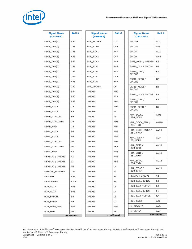
Signal Name(LPDDR3)
Ball #
DDI1_TXN[3] A57
DDI1_TXP[0] C55
DDI1_TXP[1] C58
DDI1_TXP[2] A55
DDI1_TXP[3] B57
DDI2_TXN[0] C51
DDI2_TXN[1] C53
DDI2_TXN[2] C49
DDI2_TXN[3] A53
DDI2_TXP[0] C50
DDI2_TXP[1] B54
DDI2_TXP[2] B50
DDI2_TXP[3] B53
DDPB_AUXN C5
DDPB_AUXP B5
DDPB_CTRLCLK B9
DDPB_CTRLDATA C9
DDPB_HPD C8
DDPC_AUXN B6
DDPC_AUXP A6
DDPC_CTRLCLK D9
DDPC_CTRLDATA D11
DDPC_HPD A8
DEVSLP0 / GPIO33 P2
DEVSLP1 / GPIO38 L2
DEVSLP2 / GPIO39 N5
DIFFCLK_BIASREF C26
DPWROK AV5
DSWVRMEN AW7
EDP_AUXN A45
EDP_AUXP B45
eDP_BKLCTL B8
eDP_BKLEN A9
EDP_DISP_UTIL A43
EDP_HPD D6
continued...
Signal Name(LPDDR3)
Ball #
EDP_RCOMP D20
EDP_TXN0 C45
EDP_TXN1 A47
EDP_TXN2 C47
EDP_TXN3 A49
EDP_TXP0 B46
EDP_TXP1 B47
EDP_TXP2 C46
EDP_TXP3 B49
eDP_VDDEN C6
GPIO10 AM2
GPIO13 AT3
GPIO14 AH4
GPIO15 AD6
GPIO16 Y1
GPIO17 T3
GPIO24 AD5
GPIO25 AM4
GPIO26 AN3
GPIO27 AN5
GPIO28 AD7
GPIO44 AK4
GPIO45 AG5
GPIO46 AG3
GPIO47 AB6
GPIO48 U4
GPIO49 Y3
GPIO50 P3
GPIO51 R5
GPIO52 L1
GPIO53 L4
GPIO54 L3
GPIO55 U7
GPIO56 AG6
GPIO57 AP1
continued...
Signal Name(LPDDR3)
Ball #
GPIO58 AL4
GPIO59 AT5
GPIO8 AU2
GPIO9 AM3
GSPI_MOSI / GPIO90 K2
GSPI0_CLK / GPIO84 L6
GSPI0_CS# /GPIO83
R6
GSPI0_MISO /GPIO85
N6
GSPI0_MOSI /GPIO86
L8
GSPI1_CLK / GPIO88 L5
GSPI1_CS# /GPIO87
R7
GSPI1_MISO /GPIO89
N7
HDA_BCLK /I2S0_SCLK
AW8
HDA_DOCK_EN# /I2S1_TXD
AW10
HDA_DOCK_RST# /I2S1_SFRM
AV10
HDA_RST# /I2S_MCLK
AU8
HDA_SDI0 /I2S0_RXD
AY10
HDA_SDI1 /I2S1_RXD
AU12
HDA_SDO /I2S0_TXD
AU11
HDA_SYNC /I2S0_SFRM
AV11
HSIOPC / GPIO71 Y2
I2C0_SCL / GPIO5 F3
I2C0_SDA / GPIO4 F2
I2C1_SCL / GPIO7 F1
I2C1_SDA / GPIO6 G4
I2S1_SCLK AY8
INTRUDER# AU6
INTVRMEN AV7
continued...
Processor—Processor Ball and Signal Information
5th Generation Intel® Core™ Processor Family, Intel® Core™ M Processor Family, Mobile Intel® Pentium® Processor Family, andMobile Intel® Celeron® Processor FamilyDatasheet – Volume 1 of 2 June 2015124 Order No.: 330834-005v1
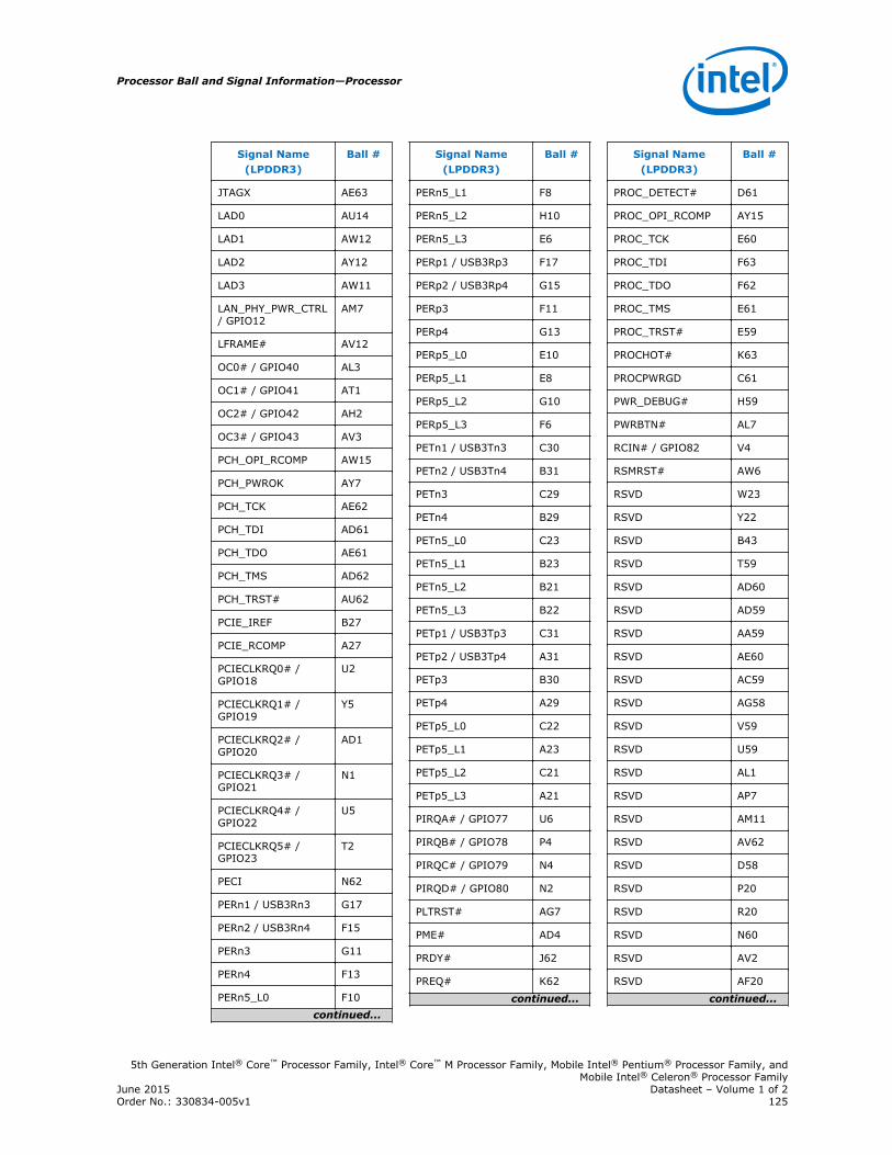
Signal Name(LPDDR3)
Ball #
JTAGX AE63
LAD0 AU14
LAD1 AW12
LAD2 AY12
LAD3 AW11
LAN_PHY_PWR_CTRL/ GPIO12
AM7
LFRAME# AV12
OC0# / GPIO40 AL3
OC1# / GPIO41 AT1
OC2# / GPIO42 AH2
OC3# / GPIO43 AV3
PCH_OPI_RCOMP AW15
PCH_PWROK AY7
PCH_TCK AE62
PCH_TDI AD61
PCH_TDO AE61
PCH_TMS AD62
PCH_TRST# AU62
PCIE_IREF B27
PCIE_RCOMP A27
PCIECLKRQ0# /GPIO18
U2
PCIECLKRQ1# /GPIO19
Y5
PCIECLKRQ2# /GPIO20
AD1
PCIECLKRQ3# /GPIO21
N1
PCIECLKRQ4# /GPIO22
U5
PCIECLKRQ5# /GPIO23
T2
PECI N62
PERn1 / USB3Rn3 G17
PERn2 / USB3Rn4 F15
PERn3 G11
PERn4 F13
PERn5_L0 F10
continued...
Signal Name(LPDDR3)
Ball #
PERn5_L1 F8
PERn5_L2 H10
PERn5_L3 E6
PERp1 / USB3Rp3 F17
PERp2 / USB3Rp4 G15
PERp3 F11
PERp4 G13
PERp5_L0 E10
PERp5_L1 E8
PERp5_L2 G10
PERp5_L3 F6
PETn1 / USB3Tn3 C30
PETn2 / USB3Tn4 B31
PETn3 C29
PETn4 B29
PETn5_L0 C23
PETn5_L1 B23
PETn5_L2 B21
PETn5_L3 B22
PETp1 / USB3Tp3 C31
PETp2 / USB3Tp4 A31
PETp3 B30
PETp4 A29
PETp5_L0 C22
PETp5_L1 A23
PETp5_L2 C21
PETp5_L3 A21
PIRQA# / GPIO77 U6
PIRQB# / GPIO78 P4
PIRQC# / GPIO79 N4
PIRQD# / GPIO80 N2
PLTRST# AG7
PME# AD4
PRDY# J62
PREQ# K62
continued...
Signal Name(LPDDR3)
Ball #
PROC_DETECT# D61
PROC_OPI_RCOMP AY15
PROC_TCK E60
PROC_TDI F63
PROC_TDO F62
PROC_TMS E61
PROC_TRST# E59
PROCHOT# K63
PROCPWRGD C61
PWR_DEBUG# H59
PWRBTN# AL7
RCIN# / GPIO82 V4
RSMRST# AW6
RSVD W23
RSVD Y22
RSVD B43
RSVD T59
RSVD AD60
RSVD AD59
RSVD AA59
RSVD AE60
RSVD AC59
RSVD AG58
RSVD V59
RSVD U59
RSVD AL1
RSVD AP7
RSVD AM11
RSVD AV62
RSVD D58
RSVD P20
RSVD R20
RSVD N60
RSVD AV2
RSVD AF20
continued...
Processor Ball and Signal Information—Processor
5th Generation Intel® Core™ Processor Family, Intel® Core™ M Processor Family, Mobile Intel® Pentium® Processor Family, andMobile Intel® Celeron® Processor Family
June 2015 Datasheet – Volume 1 of 2Order No.: 330834-005v1 125
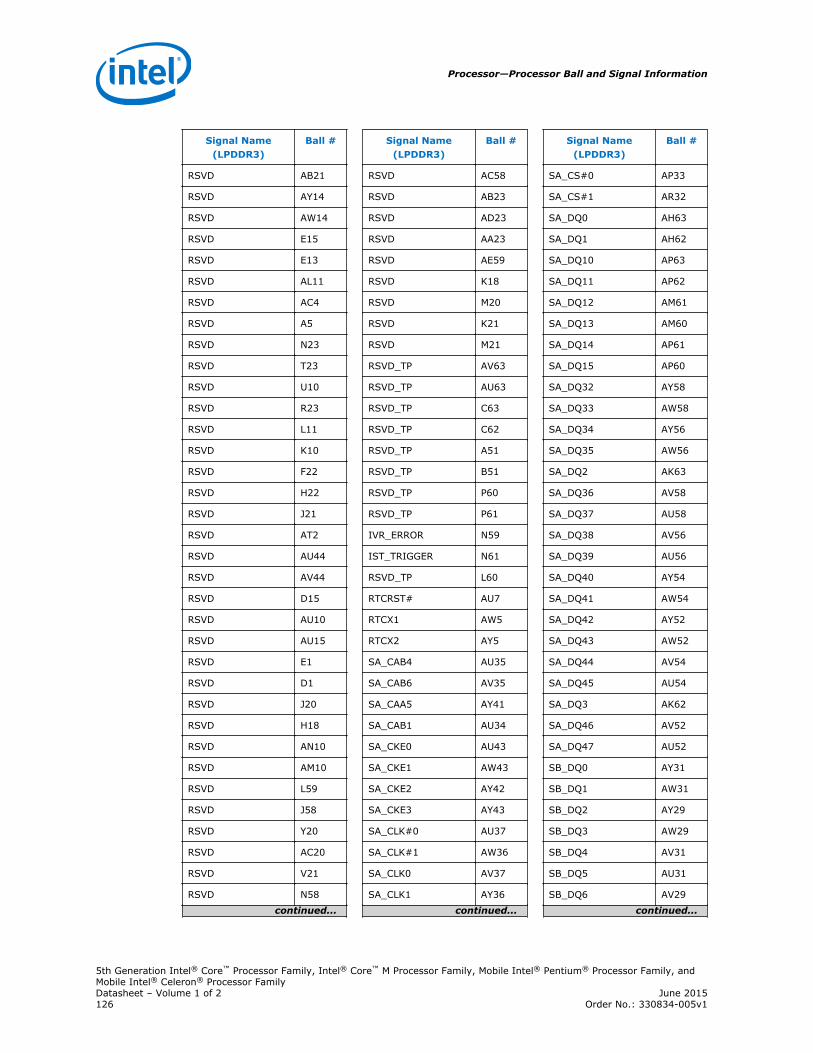
Signal Name(LPDDR3)
Ball #
RSVD AB21
RSVD AY14
RSVD AW14
RSVD E15
RSVD E13
RSVD AL11
RSVD AC4
RSVD A5
RSVD N23
RSVD T23
RSVD U10
RSVD R23
RSVD L11
RSVD K10
RSVD F22
RSVD H22
RSVD J21
RSVD AT2
RSVD AU44
RSVD AV44
RSVD D15
RSVD AU10
RSVD AU15
RSVD E1
RSVD D1
RSVD J20
RSVD H18
RSVD AN10
RSVD AM10
RSVD L59
RSVD J58
RSVD Y20
RSVD AC20
RSVD V21
RSVD N58
continued...
Signal Name(LPDDR3)
Ball #
RSVD AC58
RSVD AB23
RSVD AD23
RSVD AA23
RSVD AE59
RSVD K18
RSVD M20
RSVD K21
RSVD M21
RSVD_TP AV63
RSVD_TP AU63
RSVD_TP C63
RSVD_TP C62
RSVD_TP A51
RSVD_TP B51
RSVD_TP P60
RSVD_TP P61
IVR_ERROR N59
IST_TRIGGER N61
RSVD_TP L60
RTCRST# AU7
RTCX1 AW5
RTCX2 AY5
SA_CAB4 AU35
SA_CAB6 AV35
SA_CAA5 AY41
SA_CAB1 AU34
SA_CKE0 AU43
SA_CKE1 AW43
SA_CKE2 AY42
SA_CKE3 AY43
SA_CLK#0 AU37
SA_CLK#1 AW36
SA_CLK0 AV37
SA_CLK1 AY36
continued...
Signal Name(LPDDR3)
Ball #
SA_CS#0 AP33
SA_CS#1 AR32
SA_DQ0 AH63
SA_DQ1 AH62
SA_DQ10 AP63
SA_DQ11 AP62
SA_DQ12 AM61
SA_DQ13 AM60
SA_DQ14 AP61
SA_DQ15 AP60
SA_DQ32 AY58
SA_DQ33 AW58
SA_DQ34 AY56
SA_DQ35 AW56
SA_DQ2 AK63
SA_DQ36 AV58
SA_DQ37 AU58
SA_DQ38 AV56
SA_DQ39 AU56
SA_DQ40 AY54
SA_DQ41 AW54
SA_DQ42 AY52
SA_DQ43 AW52
SA_DQ44 AV54
SA_DQ45 AU54
SA_DQ3 AK62
SA_DQ46 AV52
SA_DQ47 AU52
SB_DQ0 AY31
SB_DQ1 AW31
SB_DQ2 AY29
SB_DQ3 AW29
SB_DQ4 AV31
SB_DQ5 AU31
SB_DQ6 AV29
continued...
Processor—Processor Ball and Signal Information
5th Generation Intel® Core™ Processor Family, Intel® Core™ M Processor Family, Mobile Intel® Pentium® Processor Family, andMobile Intel® Celeron® Processor FamilyDatasheet – Volume 1 of 2 June 2015126 Order No.: 330834-005v1
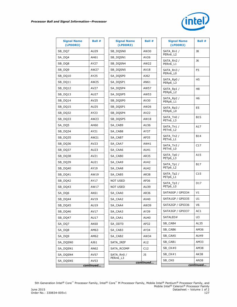
Signal Name(LPDDR3)
Ball #
SB_DQ7 AU29
SA_DQ4 AH61
SB_DQ8 AY27
SB_DQ9 AW27
SB_DQ10 AY25
SB_DQ11 AW25
SB_DQ12 AV27
SB_DQ13 AU27
SB_DQ14 AV25
SB_DQ15 AU25
SB_DQ32 AY23
SB_DQ33 AW23
SA_DQ5 AH60
SB_DQ34 AY21
SB_DQ35 AW21
SB_DQ36 AV23
SB_DQ37 AU23
SB_DQ38 AV21
SB_DQ39 AU21
SB_DQ40 AY19
SB_DQ41 AW19
SB_DQ42 AY17
SB_DQ43 AW17
SA_DQ6 AK61
SB_DQ44 AV19
SB_DQ45 AU19
SB_DQ46 AV17
SB_DQ47 AU17
SA_DQ7 AK60
SA_DQ8 AM63
SA_DQ9 AM62
SA_DQSN0 AJ61
SA_DQSN1 AN62
SA_DQSN4 AV57
SA_DQSN5 AV53
continued...
Signal Name(LPDDR3)
Ball #
SB_DQSN0 AW30
SB_DQSN1 AV26
SB_DQSN4 AW22
SB_DQSN5 AV18
SA_DQSP0 AJ62
SA_DQSP1 AN61
SA_DQSP4 AW57
SA_DQSP5 AW53
SB_DQSP0 AV30
SB_DQSP1 AW26
SB_DQSP4 AV22
SB_DQSP5 AW18
SA_CAB9 AU36
SA_CAB8 AY37
SA_CAB7 AP35
SA_CAA7 AW41
SA_CAA6 AU41
SA_CAB0 AR35
SA_CAA9 AV42
SA_CAA8 AU42
SA_CAB5 AR38
NOT USED AP36
NOT USED AU39
SA_CAA0 AR36
SA_CAA2 AV40
SA_CAA4 AW39
SA_CAA3 AY39
SA_CAA1 AU40
SA_ODT0 AP32
SA_CAB3 AY34
SA_CAB2 AW34
SATA_IREF A12
SATA_RCOMP C12
SATA_Rn0 /PERn6_L3
J5
continued...
Signal Name(LPDDR3)
Ball #
SATA_Rn1 /PERn6_L2
J8
SATA_Rn2 /PERn6_L1
J6
SATA_Rn3 /PERn6_L0
F5
SATA_Rp0 /PERp6_L3
H5
SATA_Rp1 /PERp6_L2
H8
SATA_Rp2 /PERp6_L1
H6
SATA_Rp3 /PERp6_L0
E5
SATA_Tn0 /PETn6_L3
B15
SATA_Tn1 /PETn6_L2
A17
SATA_Tn2 /PETn6_L1
B14
SATA_Tn3 /PETn6_L0
C17
SATA_Tp0 /PETp6_L3
A15
SATA_Tp1 /PETp6_L2
B17
SATA_Tp2 /PETp6_L1
C15
SATA_Tp3 /PETp6_L0
D17
SATA0GP / GPIO34 V1
SATA1GP / GPIO35 U1
SATA2GP / GPIO36 V6
SATA3GP / GPIO37 AC1
SATALED# U3
SB_CAB4 AL35
SB_CAB6 AM36
SB_CAA5 AU49
SB_CAB1 AM33
SB_CK#0 AM38
SB_CK#1 AK38
SB_CK0 AN38
continued...
Processor Ball and Signal Information—Processor
5th Generation Intel® Core™ Processor Family, Intel® Core™ M Processor Family, Mobile Intel® Pentium® Processor Family, andMobile Intel® Celeron® Processor Family
June 2015 Datasheet – Volume 1 of 2Order No.: 330834-005v1 127
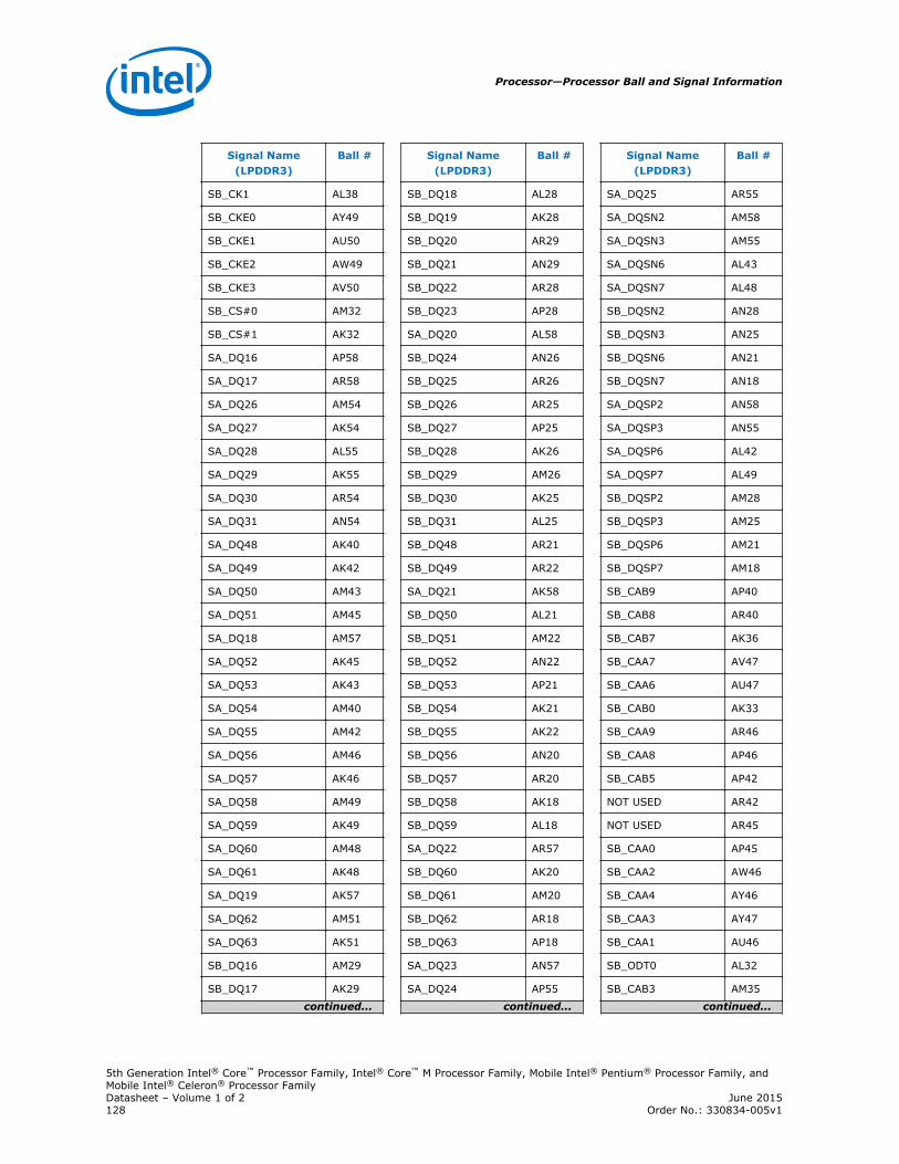
Signal Name(LPDDR3)
Ball #
SB_CK1 AL38
SB_CKE0 AY49
SB_CKE1 AU50
SB_CKE2 AW49
SB_CKE3 AV50
SB_CS#0 AM32
SB_CS#1 AK32
SA_DQ16 AP58
SA_DQ17 AR58
SA_DQ26 AM54
SA_DQ27 AK54
SA_DQ28 AL55
SA_DQ29 AK55
SA_DQ30 AR54
SA_DQ31 AN54
SA_DQ48 AK40
SA_DQ49 AK42
SA_DQ50 AM43
SA_DQ51 AM45
SA_DQ18 AM57
SA_DQ52 AK45
SA_DQ53 AK43
SA_DQ54 AM40
SA_DQ55 AM42
SA_DQ56 AM46
SA_DQ57 AK46
SA_DQ58 AM49
SA_DQ59 AK49
SA_DQ60 AM48
SA_DQ61 AK48
SA_DQ19 AK57
SA_DQ62 AM51
SA_DQ63 AK51
SB_DQ16 AM29
SB_DQ17 AK29
continued...
Signal Name(LPDDR3)
Ball #
SB_DQ18 AL28
SB_DQ19 AK28
SB_DQ20 AR29
SB_DQ21 AN29
SB_DQ22 AR28
SB_DQ23 AP28
SA_DQ20 AL58
SB_DQ24 AN26
SB_DQ25 AR26
SB_DQ26 AR25
SB_DQ27 AP25
SB_DQ28 AK26
SB_DQ29 AM26
SB_DQ30 AK25
SB_DQ31 AL25
SB_DQ48 AR21
SB_DQ49 AR22
SA_DQ21 AK58
SB_DQ50 AL21
SB_DQ51 AM22
SB_DQ52 AN22
SB_DQ53 AP21
SB_DQ54 AK21
SB_DQ55 AK22
SB_DQ56 AN20
SB_DQ57 AR20
SB_DQ58 AK18
SB_DQ59 AL18
SA_DQ22 AR57
SB_DQ60 AK20
SB_DQ61 AM20
SB_DQ62 AR18
SB_DQ63 AP18
SA_DQ23 AN57
SA_DQ24 AP55
continued...
Signal Name(LPDDR3)
Ball #
SA_DQ25 AR55
SA_DQSN2 AM58
SA_DQSN3 AM55
SA_DQSN6 AL43
SA_DQSN7 AL48
SB_DQSN2 AN28
SB_DQSN3 AN25
SB_DQSN6 AN21
SB_DQSN7 AN18
SA_DQSP2 AN58
SA_DQSP3 AN55
SA_DQSP6 AL42
SA_DQSP7 AL49
SB_DQSP2 AM28
SB_DQSP3 AM25
SB_DQSP6 AM21
SB_DQSP7 AM18
SB_CAB9 AP40
SB_CAB8 AR40
SB_CAB7 AK36
SB_CAA7 AV47
SB_CAA6 AU47
SB_CAB0 AK33
SB_CAA9 AR46
SB_CAA8 AP46
SB_CAB5 AP42
NOT USED AR42
NOT USED AR45
SB_CAA0 AP45
SB_CAA2 AW46
SB_CAA4 AY46
SB_CAA3 AY47
SB_CAA1 AU46
SB_ODT0 AL32
SB_CAB3 AM35
continued...
Processor—Processor Ball and Signal Information
5th Generation Intel® Core™ Processor Family, Intel® Core™ M Processor Family, Mobile Intel® Pentium® Processor Family, andMobile Intel® Celeron® Processor FamilyDatasheet – Volume 1 of 2 June 2015128 Order No.: 330834-005v1
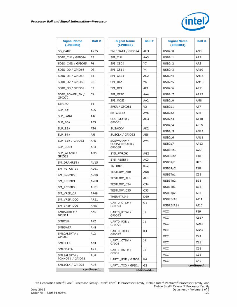
Signal Name(LPDDR3)
Ball #
SB_CAB2 AK35
SDIO_CLK / GPIO64 E3
SDIO_CMD / GPIO65 F4
SDIO_D0 / GPIO66 D3
SDIO_D1 / GPIO67 E4
SDIO_D2 / GPIO68 C3
SDIO_D3 / GPIO69 E2
SDIO_POWER_EN /GPIO70
C4
SERIRQ T4
SLP_A# AL5
SLP_LAN# AJ7
SLP_S0# AF3
SLP_S3# AT4
SLP_S4# AJ6
SLP_S5# / GPIO63 AP5
SLP_SUS# AP4
SLP_WLAN# /GPIO29
AM5
SM_DRAMRST# AV15
SM_PG_CNTL1 AV61
SM_RCOMP0 AU60
SM_RCOMP1 AV60
SM_RCOMP2 AU61
SM_VREF_CA AP49
SM_VREF_DQ0 AR51
SM_VREF_DQ1 AP51
SMBALERT# /GPIO11
AN2
SMBCLK AP2
SMBDATA AH1
SML0ALERT# /GPIO60
AL2
SML0CLK AN1
SML0DATA AK1
SML1ALERT# /PCHHOT# / GPIO73
AU4
SML1CLK / GPIO75 AU3
continued...
Signal Name(LPDDR3)
Ball #
SML1DATA / GPIO74 AH3
SPI_CLK AA3
SPI_CS0# Y7
SPI_CS1# Y4
SPI_CS2# AC2
SPI_IO2 Y6
SPI_IO3 AF1
SPI_MISO AA4
SPI_MOSI AA2
SPKR / GPIO81 V2
SRTCRST# AV6
SUS_STAT# /GPIO61
AG4
SUSACK# AK2
SUSCLK / GPIO62 AE6
SUSWARN# /SUSPWRDNACK /GPIO30
AV4
SYS_PWROK AG2
SYS_RESET# AC3
TD_IREF B12
TESTLOW_AK8 AK8
TESTLOW_AL8 AL8
TESTLOW_C34 C34
TESTLOW_C35 C35
THERMTRIP# D60
UART0_CTS# /GPIO94
G1
UART0_RTS# /GPIO93
J2
UART0_RXD /GPIO91
J1
UART0_TXD /GPIO92
K3
UART1_CTS# /GPIO3
J4
UART1_RST# /GPIO2
J3
UART1_RXD / GPIO0 K4
UART1_TXD / GPIO1 G2
continued...
Signal Name(LPDDR3)
Ball #
USB2n0 AN8
USB2n1 AR7
USB2n2 AR8
USB2n3 AR10
USB2n4 AM15
USB2n5 AM13
USB2n6 AP11
USB2n7 AR13
USB2p0 AM8
USB2p1 AT7
USB2p2 AP8
USB2p3 AT10
USB2p4 AL15
USB2p5 AN13
USB2p6 AN11
USB2p7 AP13
USB3Rn1 G20
USB3Rn2 E18
USB3Rp1 H20
USB3Rp2 F18
USB3Tn1 C33
USB3Tn2 B33
USB3Tp1 B34
USB3Tp2 A33
USBRBIAS AJ11
USBRBIAS# AJ10
VCC F59
VCC AB57
VCC AD57
VCC AG57
VCC C24
VCC C28
VCC C32
VCC C36
VCC C40
continued...
Processor Ball and Signal Information—Processor
5th Generation Intel® Core™ Processor Family, Intel® Core™ M Processor Family, Mobile Intel® Pentium® Processor Family, andMobile Intel® Celeron® Processor Family
June 2015 Datasheet – Volume 1 of 2Order No.: 330834-005v1 129
Signal Name(LPDDR3)
Ball #
VCC C44
VCC C48
VCC C52
VCC C56
VCC E23
VCC E25
VCC E27
VCC E29
VCC E31
VCC E33
VCC E35
VCC E37
VCC E39
VCC E41
VCC E43
VCC E45
VCC E47
VCC E49
VCC E51
VCC E53
VCC E55
VCC E57
VCC F24
VCC F28
VCC F32
VCC F36
VCC F40
VCC F44
VCC F48
VCC F52
VCC F56
VCC G23
VCC G25
VCC G27
VCC G29
continued...
Signal Name(LPDDR3)
Ball #
VCC G31
VCC G33
VCC G35
VCC G37
VCC G39
VCC G41
VCC G43
VCC G45
VCC G47
VCC G49
VCC G51
VCC G53
VCC G55
VCC G57
VCC H23
VCC J23
VCC K23
VCC K57
VCC L22
VCC M23
VCC M57
VCC P57
VCC U57
VCC W57
VCC_SENSE E63
VCC1_05 P9
VCC1_05 N8
VCC1_05 AE8
VCC1_05 AF22
VCC1_05 H11
VCC1_05 H15
VCC1_05 J11
VCC1_05 AG16
VCC1_05 AG17
VCC3_3 V8
continued...
Signal Name(LPDDR3)
Ball #
VCC3_3 W9
VCC3_3 K14
VCC3_3 K16
VCCACLKPLL A20
VCCAPLL AA21
VCCAPLL W21
VCCASW AE9
VCCASW AF9
VCCASW AG8
VCCASW AG13
VCCASW AG14
VCCCLK J18
VCCCLK K19
VCCCLK J17
VCCCLK T21
VCCCLK R21
VCCDSW3_3 AH10
VCCHDA AH14
VCCHSIO M9
VCCHSIO K9
VCCHSIO L10
VCCIO_OUT A59
VCOMP_OUT E20
VCCRTC AG10
VCCSATA3PLL B11
VCCSDIO U8
VCCSDIO T9
VCCSPI Y8
VCCST AC22
VCCST AE22
VCCST AE23
VCCST_PWRGD B59
VCCSUS3_3 AH11
VCCSUS3_3 AA9
VCCSUS3_3 AC9
continued...
Processor—Processor Ball and Signal Information
5th Generation Intel® Core™ Processor Family, Intel® Core™ M Processor Family, Mobile Intel® Pentium® Processor Family, andMobile Intel® Celeron® Processor FamilyDatasheet – Volume 1 of 2 June 2015130 Order No.: 330834-005v1
Signal Name(LPDDR3)
Ball #
VCCSUS3_3 AE20
VCCSUS3_3 AE21
VCCTS1_5 J15
VCCUSB3PLL B18
VDDQ AH26
VDDQ AJ31
VDDQ AJ33
VDDQ AJ37
VDDQ AN33
VDDQ AP43
VDDQ AR48
VDDQ AY35
VDDQ AY40
VDDQ AY44
VDDQ AY50
VIDALERT# L62
VIDSCLK N63
VIDSOUT L63
VR_EN F60
VR_READY C59
VSS P62
VSS D63
VSS P22
VSS N21
VSS A11
VSS A14
VSS A18
VSS A24
VSS A28
VSS A32
VSS A36
VSS A40
VSS A48
VSS A52
VSS A56
continued...
Signal Name(LPDDR3)
Ball #
VSS AA1
VSS A44
VSS AA58
VSS AB10
VSS AB20
VSS AE5
VSS AB22
VSS AB7
VSS AC61
VSS AD3
VSS AD63
VSS AE10
VSS AD21
VSS AE58
VSS AR43
VSS C39
VSS AF11
VSS AF12
VSS AF14
VSS AF15
VSS AF17
VSS AF18
VSS AG21
VSS AG23
VSS AG1
VSS AG11
VSS AG60
VSS AG61
VSS AG62
VSS AG63
VSS AH17
VSS AH19
VSS AH20
VSS AH22
VSS AH24
continued...
Signal Name(LPDDR3)
Ball #
VSS AH28
VSS AH30
VSS AH32
VSS AH34
VSS AH36
VSS AH38
VSS AH40
VSS AH42
VSS AH44
VSS AH49
VSS AH51
VSS AH53
VSS AH55
VSS AH57
VSS AJ13
VSS AJ14
VSS AJ23
VSS AJ25
VSS AJ27
VSS AJ29
VSS AJ35
VSS AJ39
VSS AJ41
VSS AJ43
VSS AJ45
VSS AJ47
VSS AJ50
VSS AJ52
VSS AJ54
VSS AJ56
VSS AJ58
VSS AJ60
VSS AJ63
VSS AK23
VSS AK3
continued...
Processor Ball and Signal Information—Processor
5th Generation Intel® Core™ Processor Family, Intel® Core™ M Processor Family, Mobile Intel® Pentium® Processor Family, andMobile Intel® Celeron® Processor Family
June 2015 Datasheet – Volume 1 of 2Order No.: 330834-005v1 131
Signal Name(LPDDR3)
Ball #
VSS AK52
VSS AL10
VSS AL13
VSS AL17
VSS AL20
VSS AL22
VSS AL23
VSS AL26
VSS AL29
VSS AL31
VSS AL33
VSS AL36
VSS AL39
VSS AL40
VSS AL45
VSS AL46
VSS AL51
VSS AL52
VSS AL54
VSS AL57
VSS AL60
VSS AL61
VSS AM1
VSS AM17
VSS AM23
VSS AM31
VSS AM52
VSS AN17
VSS AN23
VSS AN31
VSS AN32
VSS AN35
VSS AN36
VSS AN39
VSS AN40
continued...
Signal Name(LPDDR3)
Ball #
VSS AN42
VSS AN43
VSS AN45
VSS AN46
VSS AN48
VSS AN49
VSS AN51
VSS AN52
VSS AN60
VSS AN63
VSS AN7
VSS AP10
VSS AP17
VSS AP20
VSS AP22
VSS AP23
VSS AP26
VSS AP29
VSS AP3
VSS AP31
VSS AP38
VSS AP39
VSS AP52
VSS AP54
VSS AP57
VSS AR11
VSS AR15
VSS AR17
VSS AR23
VSS AR31
VSS AR33
VSS AR39
VSS AP48
VSS AR49
VSS AR5
continued...
Signal Name(LPDDR3)
Ball #
VSS AR52
VSS AT13
VSS AT35
VSS AT37
VSS AT40
VSS AT42
VSS AT43
VSS AT46
VSS AT49
VSS AT61
VSS AT62
VSS AT63
VSS AU1
VSS AU16
VSS AU18
VSS AU20
VSS AU22
VSS AU24
VSS AU26
VSS AU28
VSS AU30
VSS AU33
VSS AU51
VSS AU53
VSS AU55
VSS AU57
VSS AU59
VSS AV14
VSS D62
VSS AV16
VSS AV20
VSS AV24
VSS AV28
VSS AV33
VSS AV34
continued...
Processor—Processor Ball and Signal Information
5th Generation Intel® Core™ Processor Family, Intel® Core™ M Processor Family, Mobile Intel® Pentium® Processor Family, andMobile Intel® Celeron® Processor FamilyDatasheet – Volume 1 of 2 June 2015132 Order No.: 330834-005v1
Signal Name(LPDDR3)
Ball #
VSS AV36
VSS AV39
VSS AV41
VSS AV43
VSS AV46
VSS AV49
VSS AV51
VSS AV55
VSS AV59
VSS AV8
VSS AW16
VSS AW24
VSS AW33
VSS AW35
VSS AW37
VSS AW4
VSS AW40
VSS AW42
VSS AW44
VSS AW47
VSS AW50
VSS AW51
VSS AW59
VSS AW60
VSS AY11
VSS AY16
VSS AY18
VSS AY22
VSS AY24
VSS AY26
VSS AY30
VSS AY33
VSS AY51
VSS AY53
VSS AY57
continued...
Signal Name(LPDDR3)
Ball #
VSS AY59
VSS AY6
VSS AY4
VSS B20
VSS B24
VSS B26
VSS B28
VSS B32
VSS C38
VSS B36
VSS B4
VSS B40
VSS B44
VSS C14
VSS B48
VSS B52
VSS B56
VSS B60
VSS C11
VSS C18
VSS C20
VSS C25
VSS C27
VSS D12
VSS D14
VSS D18
VSS D21
VSS D23
VSS D25
VSS D26
VSS D27
VSS D29
VSS D2
VSS D30
VSS D31
continued...
Signal Name(LPDDR3)
Ball #
VSS D33
VSS D34
VSS D35
VSS D37
VSS D38
VSS D39
VSS D41
VSS D42
VSS D43
VSS D45
VSS D46
VSS D47
VSS D49
VSS D50
VSS D51
VSS D53
VSS D54
VSS D55
VSS D57
VSS D59
VSS E11
VSS E17
VSS F42
VSS F20
VSS D5
VSS F26
VSS F30
VSS F34
VSS F38
VSS G6
VSS F46
VSS F50
VSS F54
VSS F58
VSS F61
continued...
Processor Ball and Signal Information—Processor
5th Generation Intel® Core™ Processor Family, Intel® Core™ M Processor Family, Mobile Intel® Pentium® Processor Family, andMobile Intel® Celeron® Processor Family
June 2015 Datasheet – Volume 1 of 2Order No.: 330834-005v1 133
Signal Name(LPDDR3)
Ball #
VSS G18
VSS G22
VSS G3
VSS G5
VSS G8
VSS H13
VSS H17
VSS H57
VSS J10
VSS J22
VSS J59
VSS J63
VSS K1
VSS K12
VSS R22
VSS L13
VSS L15
VSS L17
VSS L18
VSS L20
VSS L58
VSS L61
VSS L7
VSS M22
VSS N10
VSS N3
VSS C57
VSS P59
VSS P63
VSS R10
VSS R8
VSS T1
VSS T58
VSS D8
VSS U20
continued...
Signal Name(LPDDR3)
Ball #
VSS U22
VSS U61
VSS V10
VSS V3
VSS V7
VSS W20
VSS Y10
VSS U9
VSS Y59
VSS Y63
VSS W22
VSS V58
VSS AH46
VSS V23
VSS AH16
VSS_SENSE E62
WAKE# AJ5
XTAL24_IN A25
XTAL24_OUT B25
Processor—Processor Ball and Signal Information
5th Generation Intel® Core™ Processor Family, Intel® Core™ M Processor Family, Mobile Intel® Pentium® Processor Family, andMobile Intel® Celeron® Processor FamilyDatasheet – Volume 1 of 2 June 2015134 Order No.: 330834-005v1