Embed Size (px)
Citation preview
5.4: A 5GHz CMOS Transceiverfor IEEE 802.11a Wireless LAN
David Su, Masoud Zargari, Patrick Yue,Shahriar Rabii, David Weber, Brian Kaczynski,Srenik Mehta, Kalwant Singh, Sunetra Mendis,
and Bruce Wooley1
Atheros Communications, Sunnyvale, California1Stanford University, Stanford, California
Outline
❑ Introduction: 802.11a Wireless LAN
❑ Architecture
❑ Radio Design• Transmitter• Receiver• Frequency Synthesizer
❑ Summary
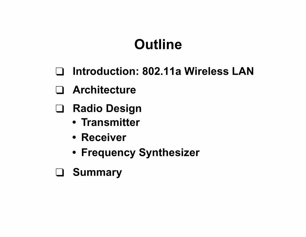
IEEE 802.11a WLAN
■ Frequency: 5 GHz UNII (Unlicensed NationalInformation Infrastructure)
■ Total UNII Bandwidth: 300 MHz (> IEEE 802.11b)
■ Modulation: OFDM(Orthogonal Frequency Division Multiplexing)+ BPSK / QPSK / 16QAM / 64QAM
■ Data Rate: 6 - 54 Mbps
5.15G 5.25G 5.35G 5.725G 5.825G
40mW200mW 800mW
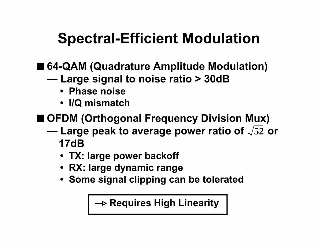
Spectral-Efficient Modulation
■ 64-QAM (Quadrature Amplitude Modulation)— Large signal to noise ratio > 30dB
• Phase noise• I/Q mismatch
■ OFDM (Orthogonal Frequency Division Mux)— Large peak to average power ratio of or
17dB• TX: large power backoff• RX: large dynamic range• Some signal clipping can be tolerated
Requires High Linearity
52
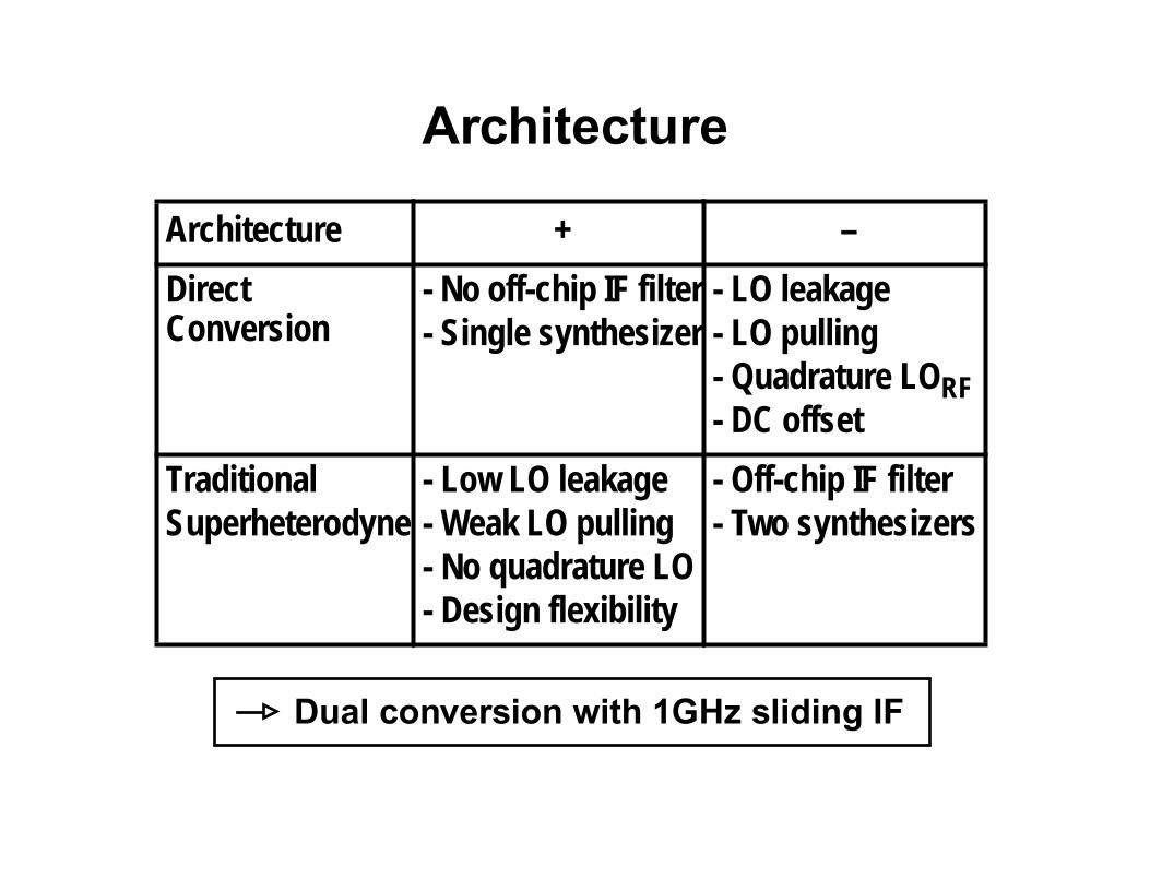
Architecture
Architecture + –
DirectConversion
- No off-chip IF filter- Single synthesizer
- LO leakage- LO pulling- Quadrature LORF- DC offset
TraditionalSuperheterodyne
- Low LO leakage- Weak LO pulling- No quadrature LO- Design flexibility
- Off-chip IF filter- Two synthesizers
Dual conversion with 1GHz sliding IF
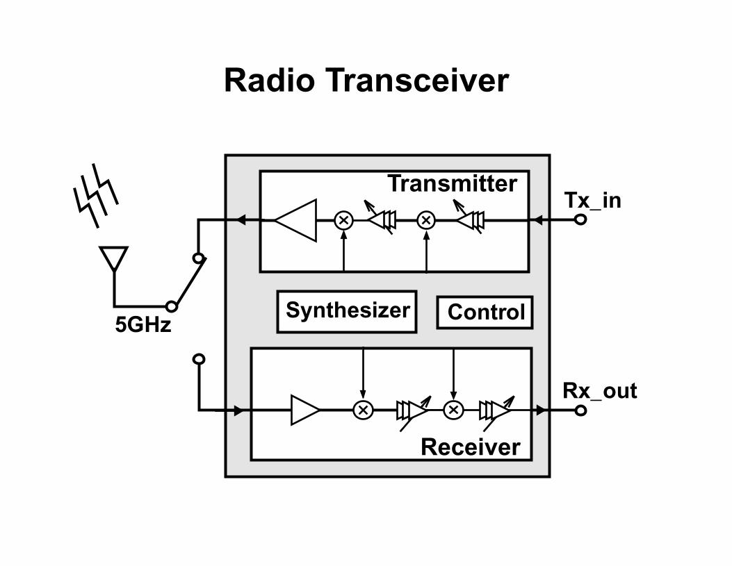
Radio Transceiver
Rx_out
Synthesizer Control5GHz
Receiver
Tx_inTransmitter
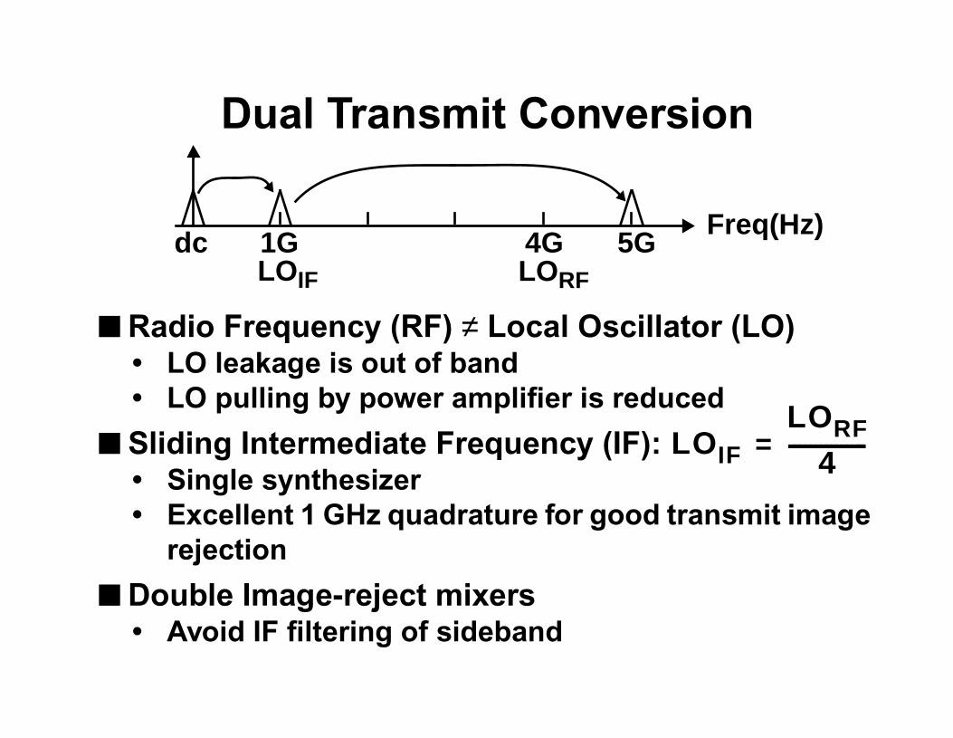
Dual Transmit Conversion
■ Radio Frequency (RF) ≠ Local Oscillator (LO)• LO leakage is out of band• LO pulling by power amplifier is reduced
■ Sliding Intermediate Frequency (IF):• Single synthesizer• Excellent 1 GHz quadrature for good transmit image
rejection
■ Double Image-reject mixers• Avoid IF filtering of sideband
LOIFLORF
4---------------=
Freq(Hz)
LORF
1G 5G4GdcLOIF
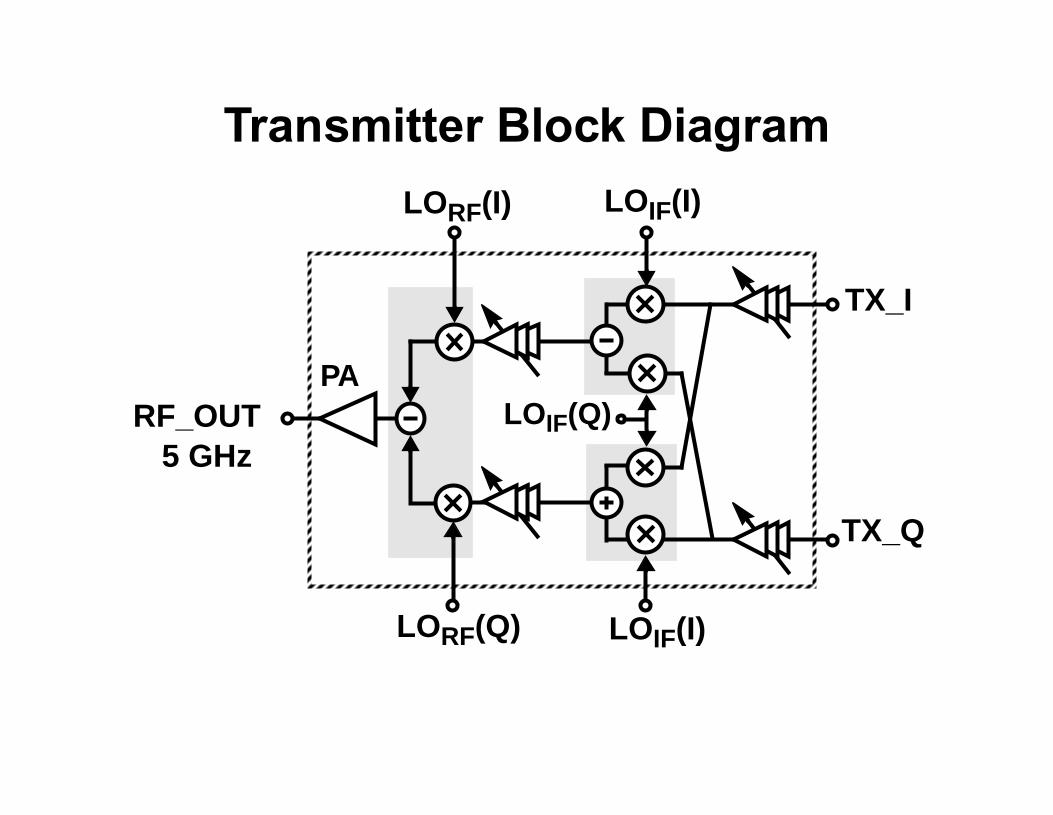
Transmitter Block Diagram
RF_OUT
LOIF(I)
PA
LORF(I)
LORF(Q)
LOIF(Q)
LOIF(I)
TX_I
TX_Q
5 GHz
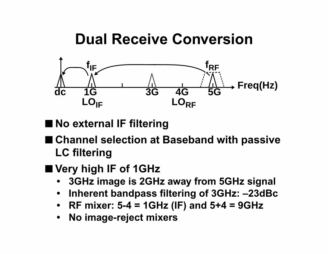
Dual Receive Conversion
■ No external IF filtering
■ Channel selection at Baseband with passiveLC filtering
■ Very high IF of 1GHz• 3GHz image is 2GHz away from 5GHz signal• Inherent bandpass filtering of 3GHz: –23dBc• RF mixer: 5-4 = 1GHz (IF) and 5+4 = 9GHz• No image-reject mixers
Freq(Hz)
fRFfIF
1G 3G 5G4GdcLORFLOIF
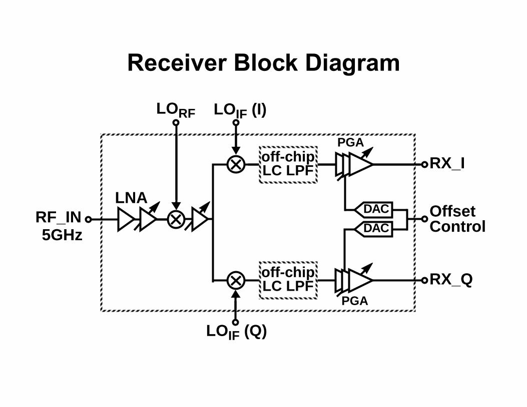
LNA
LOIF (Q)
PGA
DAC
DACRF_IN
RX_I
RX_Q
Offset
PGA
off-chip
Control
Receiver Block Diagram
5GHz
LC LPF
off-chipLC LPF
LORF LOIF (I)
Synthesizer
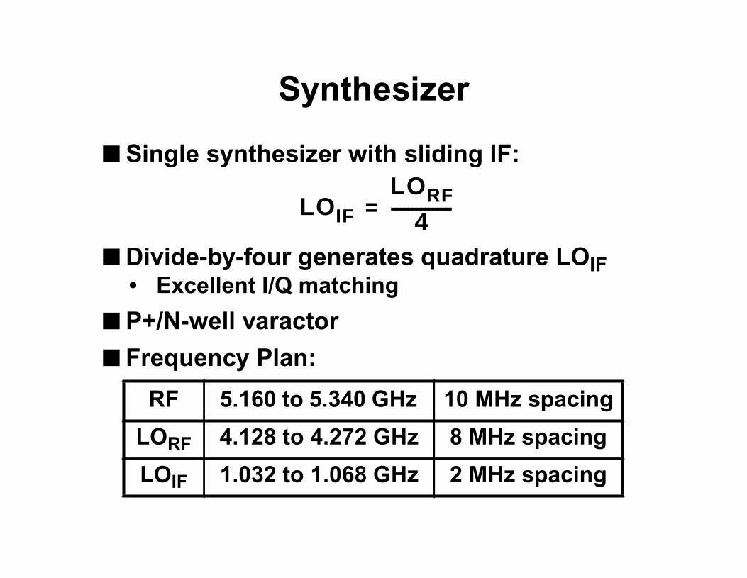
■ Single synthesizer with sliding IF:
■ Divide-by-four generates quadrature LOIF• Excellent I/Q matching
■ P+/N-well varactor
■ Frequency Plan:
LOIFLORF
4---------------=
RF 5.160 to 5.340 GHz 10 MHz spacing
LORF 4.128 to 4.272 GHz 8 MHz spacing
LOIF 1.032 to 1.068 GHz 2 MHz spacing
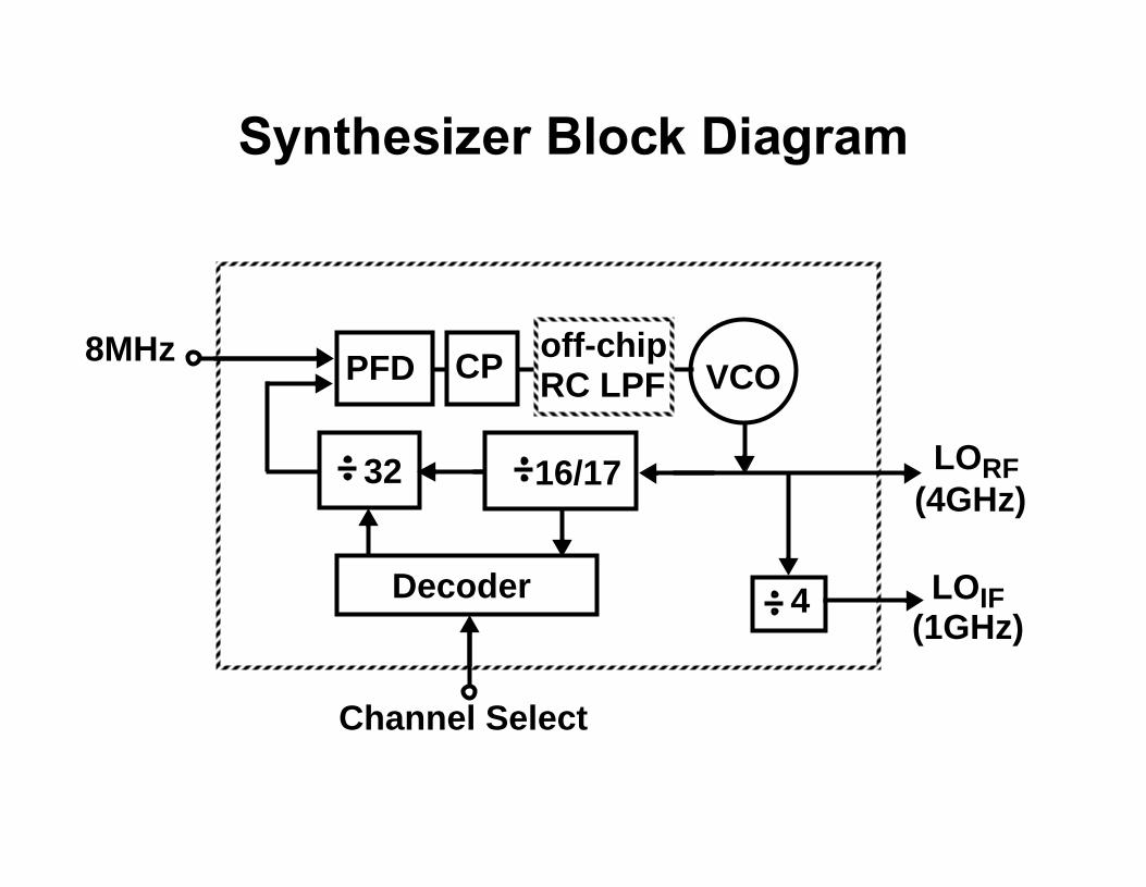
Synthesizer Block Diagram
LOIF
LORF
PFD CP VCORC LPF8MHz
32 16/17
Decoder
(4GHz)
(1GHz)
Channel Select
4
off-chip
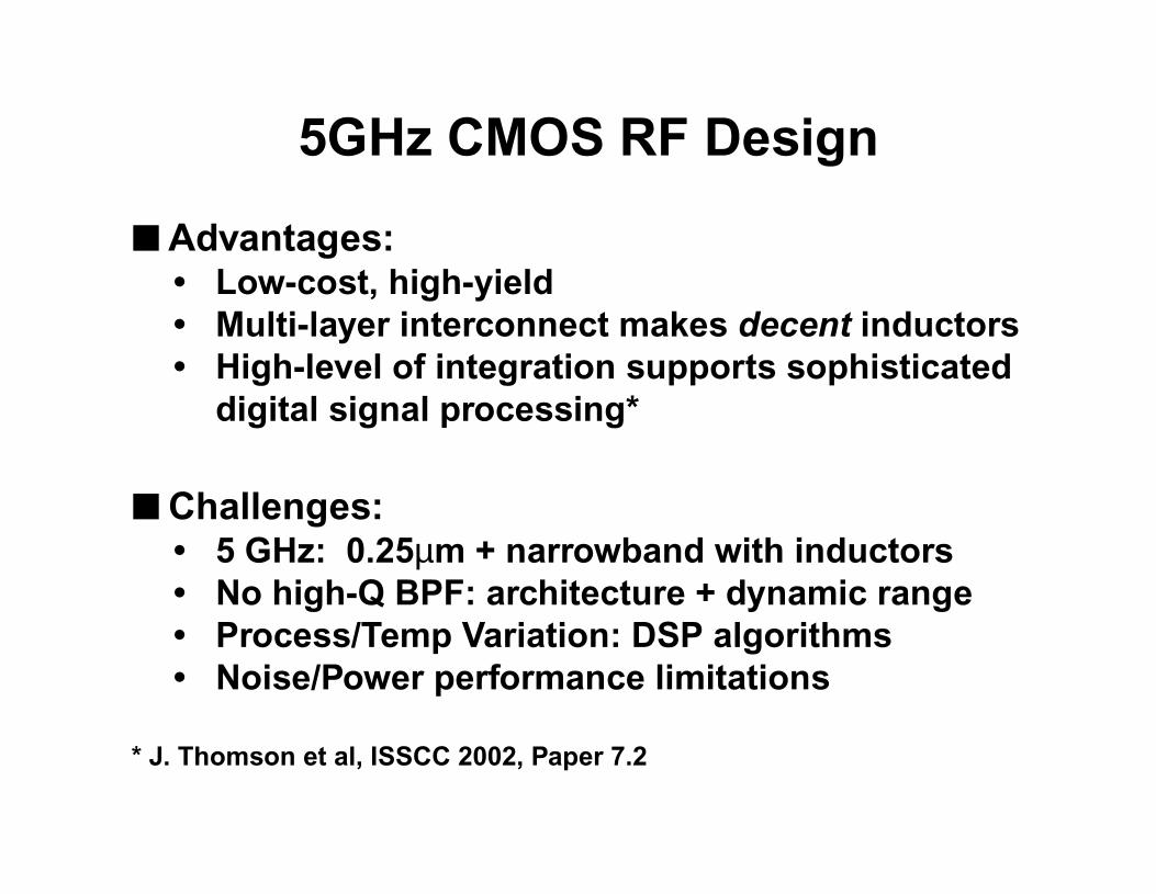
5GHz CMOS RF Design
■ Advantages:• Low-cost, high-yield• Multi-layer interconnect makes decent inductors• High-level of integration supports sophisticated
digital signal processing*
■ Challenges:• 5 GHz: 0.25µm + narrowband with inductors• No high-Q BPF: architecture + dynamic range• Process/Temp Variation: DSP algorithms• Noise/Power performance limitations
* J. Thomson et al, ISSCC 2002, Paper 7.2
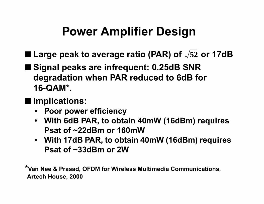
Power Amplifier Design
■ Large peak to average ratio (PAR) of or 17dB
■ Signal peaks are infrequent: 0.25dB SNRdegradation when PAR reduced to 6dB for16-QAM*.
■ Implications:• Poor power efficiency• With 6dB PAR, to obtain 40mW (16dBm) requires
Psat of ~22dBm or 160mW• With 17dB PAR, to obtain 40mW (16dBm) requires
Psat of ~33dBm or 2W
*Van Nee & Prasad, OFDM for Wireless Multimedia Communications,Artech House, 2000
52
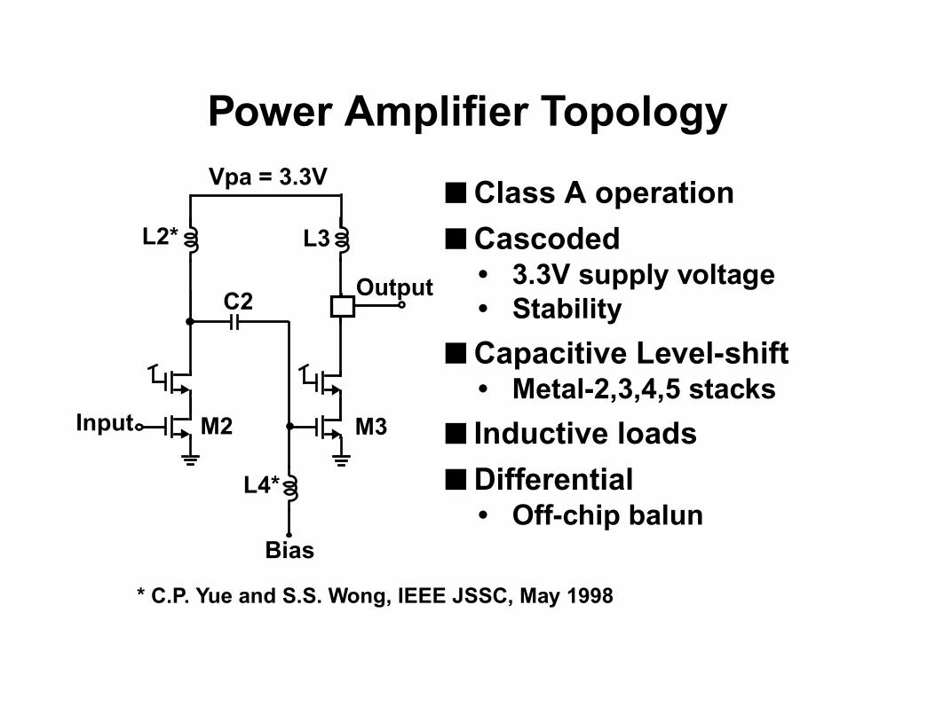
Power Amplifier Topology
Output
Bias
L3
Input
L2*
M2 M3
C2
L4*
Vpa = 3.3V■ Class A operation
■ Cascoded• 3.3V supply voltage• Stability
■ Capacitive Level-shift• Metal-2,3,4,5 stacks
■ Inductive loads
■ Differential• Off-chip balun
* C.P. Yue and S.S. Wong, IEEE JSSC, May 1998
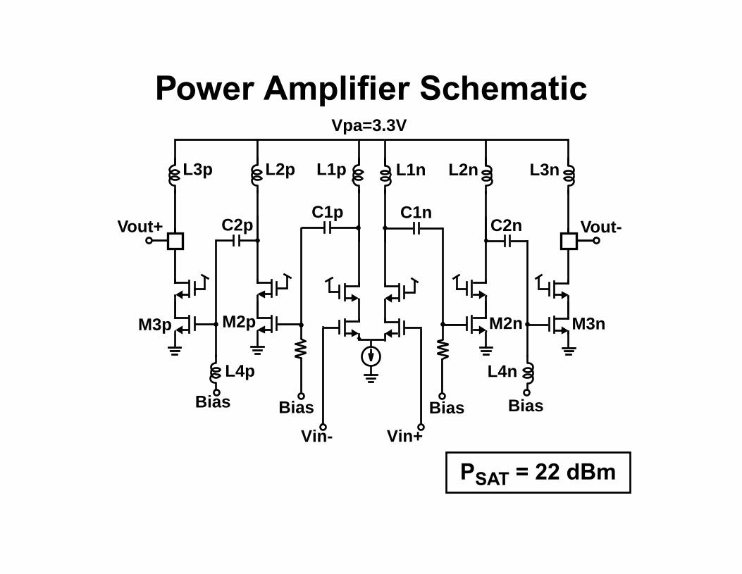
Power Amplifier Schematic
Vin+Vin-
Vpa=3.3V
L1p
C1pVout+
Bias
L3p
Bias
L2p
M2pM3p
C2p
L4p
L1n
C1nVout-
Bias
L3n
Bias
L2n
M2n M3n
C2n
L4n
PSAT = 22 dBm
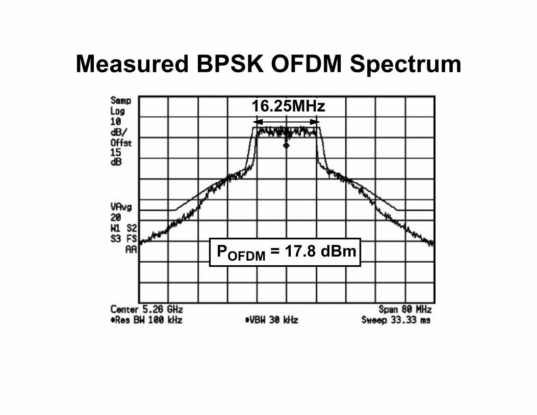
Measured BPSK OFDM Spectrum
16.25MHz
POFDM = 17.8 dBm
64QAM (300kHz) modulated signal
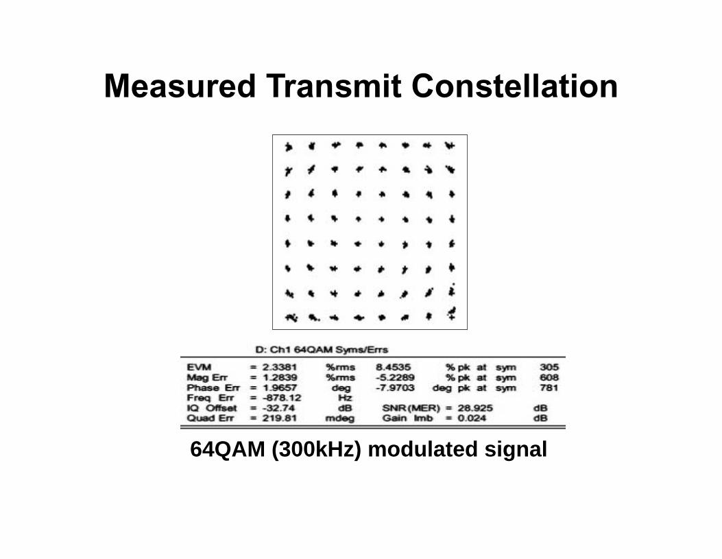
Measured Transmit Constellation
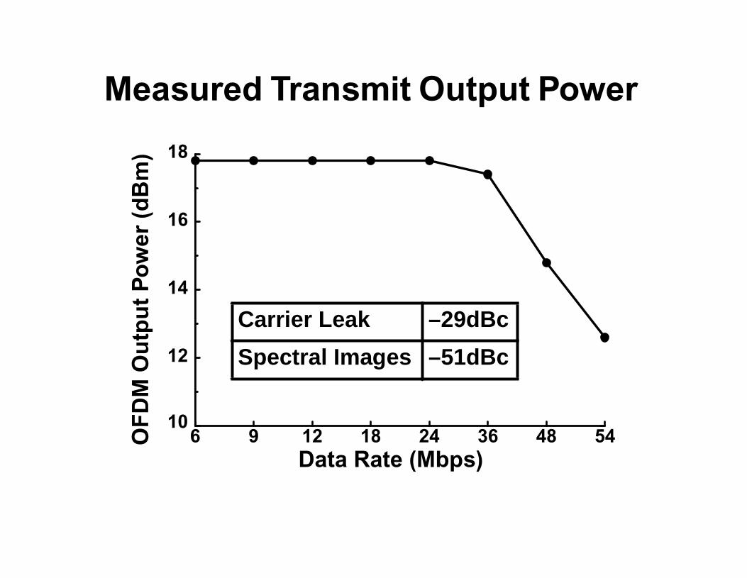
Measured Transmit Output Power
6 9 12 18 24 36 48 54
12
14
16
18O
FD
M O
utp
ut
Po
wer
(d
Bm
)
Data Rate (Mbps)
10
Carrier Leak –29dBc
Spectral Images –51dBc
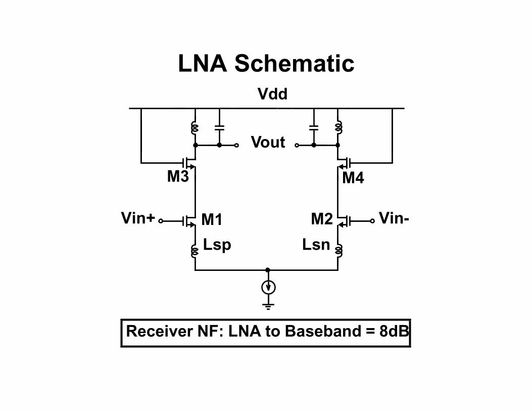
LNA Schematic
Receiver NF: LNA to Baseband = 8dB
Vin+
Vout
M3
M1 Vin-
M4
M2
Lsp Lsn
Vdd
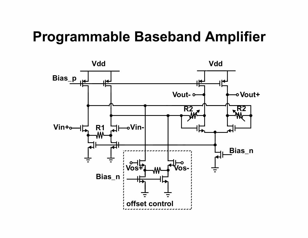
Vin+ Vin-
Vout- Vout+
Vos+ Vos-
offset control
R1
R2 R2
Vdd
Bias_p
Bias_n
Bias_n
Programmable Baseband Amplifier
Vdd
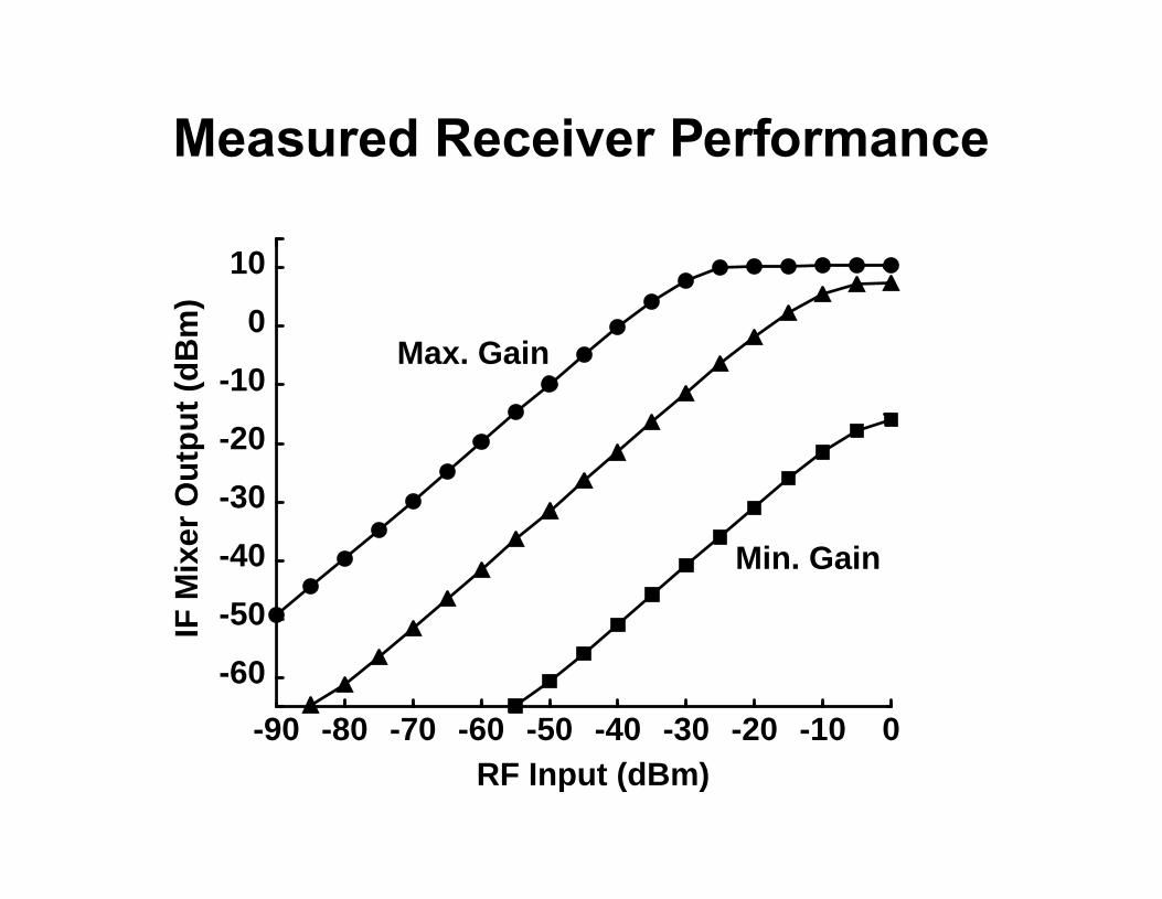
Measured Receiver Performance
-30-90 -80 -70 -60 -50 -40 -20 -10 0
-60
-50
-40
-30
-20
-10
0
10
Min. Gain
Max. Gain
RF Input (dBm)
IFM
ixer
Ou
tpu
t (d
Bm
)
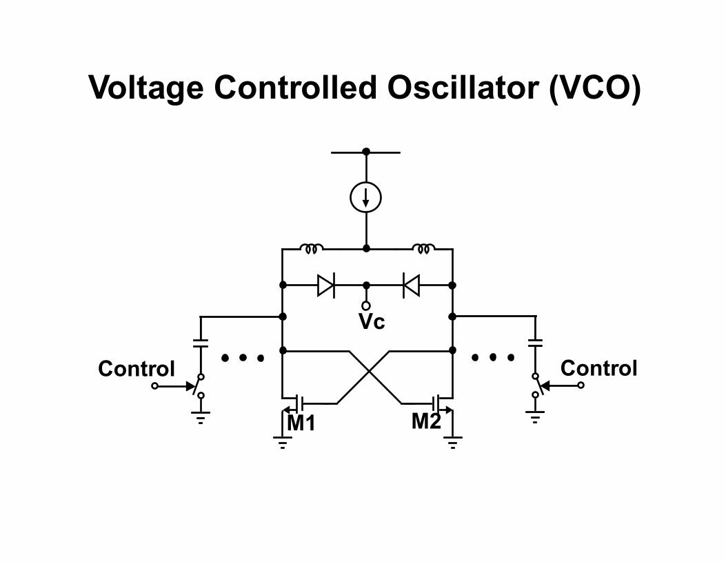
M1 M2
Vc
Control
Voltage Controlled Oscillator (VCO)
Control
Frequency (Hz)
Ph
ase
No
ise
(dB
c/H
z)
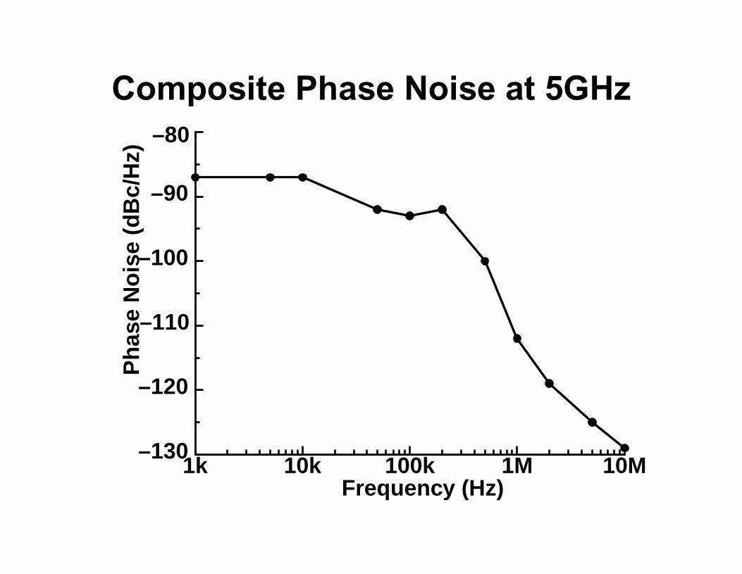
1k 10k 100k 1M 10M–130
–120
–110
–100
–90
Composite Phase Noise at 5GHz–80
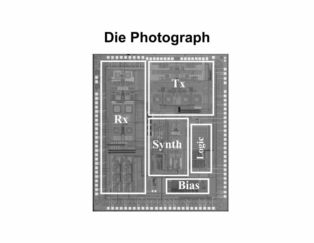
Die Photograph
Tx
Rx
Synth
BiasL
ogic
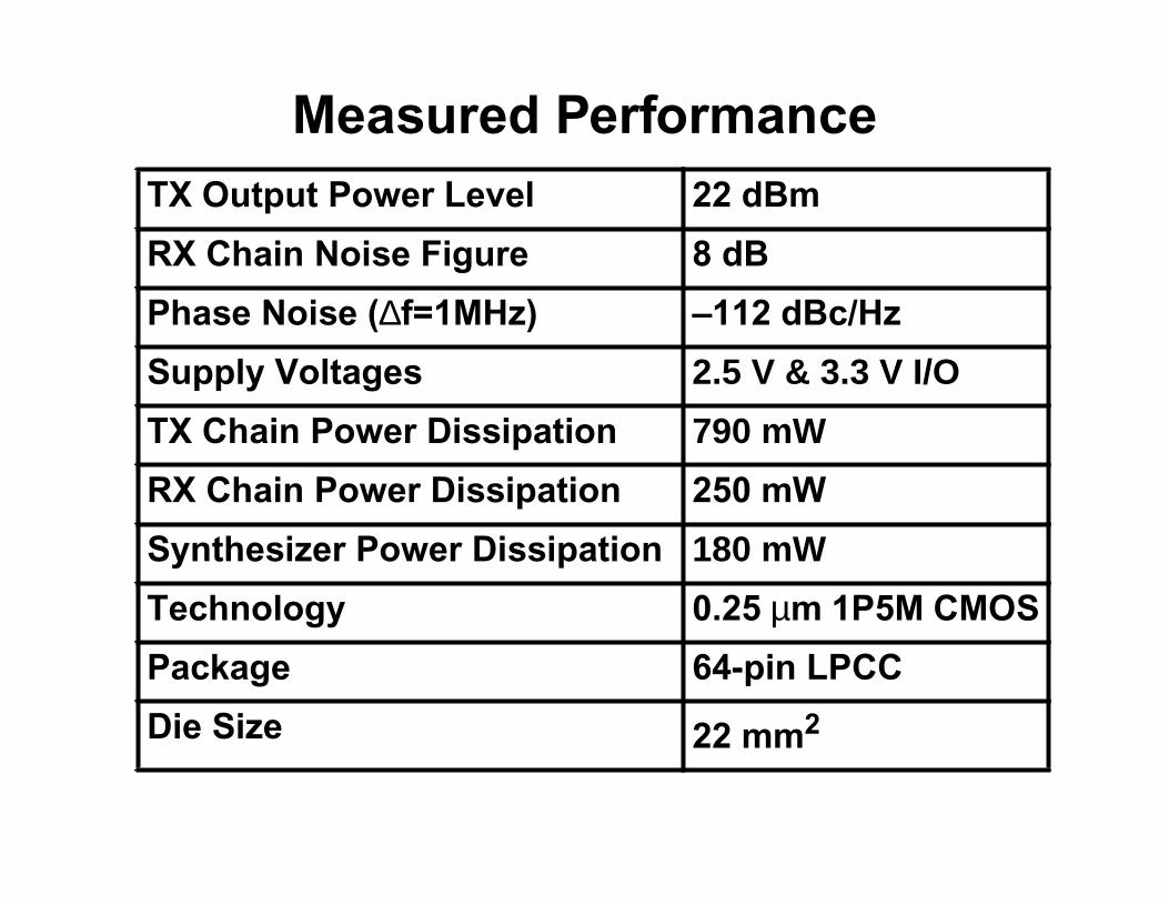
Measured PerformanceTX Output Power Level 22 dBm
RX Chain Noise Figure 8 dB
Phase Noise (∆f=1MHz) –112 dBc/Hz
Supply Voltages 2.5 V & 3.3 V I/O
TX Chain Power Dissipation 790 mW
RX Chain Power Dissipation 250 mW
Synthesizer Power Dissipation 180 mW
Technology 0.25 µm 1P5M CMOS
Package 64-pin LPCC
Die Size 22 mm2
Conclusions
■ IEEE 802.11a radio transceiver in 0.25 µmstandard digital CMOS for 5-GHz WLAN
■ No external IF filter:• TX: double image-reject mixers• RX: very high IF of 1GHz
■ Dual conversion with sliding IF: singlesynthesizer
■ Integration of:• transmitter with 22dBm output power• receiver with 8dB noise figure• synthesizer with –112dBc/Hz (∆f=1MHz)
Acknowledgement
■ Support of the Wireless Team at Atheros fordesign, layout, and testing. In particular:H. Dieh, J. Kung, R. Popescu, A. Ong,J. Zheng, D. Nakahira, R. Subramanian,J. Kuskin, A. Dao, D. Johnson, C. Lee, L. Thon,P. Husted, W. McFarland, S. Wong, R. Bahr, T.Meng
■ Assistance of TSMC. In particular: S. C. Wongand B. K. Liew.