Embed Size (px)
Citation preview
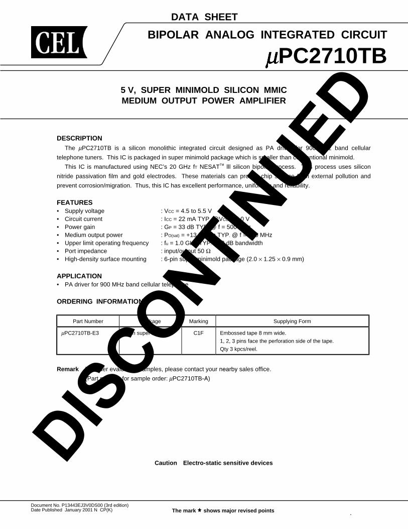
BIPOLAR ANALOG INTEGRATED CIRCUIT
µµµµPC2710TB5 V, SUPER MINIMOLD SILICON MMICMEDIUM OUTPUT POWER AMPLIFIER
Document No. P13443EJ3V0DS00 (3rd edition) Date Published January 2001 N CP(K)
DATA SHEET
DESCRIPTIONThe µPC2710TB is a silicon monolithic integrated circuit designed as PA driver for 900 MHz band cellular
telephone tuners. This IC is packaged in super minimold package which is smaller than conventional minimold.
This IC is manufactured using NEC’s 20 GHz fT NESATTM lll silicon bipolar process. This process uses silicon
nitride passivation film and gold electrodes. These materials can protect chip surface from external pollution and
prevent corrosion/migration. Thus, this IC has excellent performance, uniformity and reliability.
FEATURES• Supply voltage : VCC = 4.5 to 5.5 V• Circuit current : ICC = 22 mA TYP. @VCC = 5.0 V• Power gain : GP = 33 dB TYP. @ f = 500 MHz• Medium output power : PO(sat) = +13.5 dBm TYP. @ f = 500 MHz• Upper limit operating frequency : fu = 1.0 GHz TYP. @ 3 dB bandwidth• Port impedance : input/output 50 Ω• High-density surface mounting : 6-pin super minimold package (2.0 × 1.25 × 0.9 mm)
APPLICATION• PA driver for 900 MHz band cellular telephone
ORDERING INFORMATION
Part Number Package Marking Supplying Form
µPC2710TB-E3 6-pin super minimold C1F Embossed tape 8 mm wide.
1, 2, 3 pins face the perforation side of the tape.
Qty 3 kpcs/reel.
Remark To order evaluation samples, please contact your nearby sales office.
(Part number for sample order: µPC2710TB-A)
Caution Electro-static sensitive devices
The mark shows major revised points
DISCONTIN
UED
Data Sheet P13443EJ3V0DS2
µµµµPC2710TB
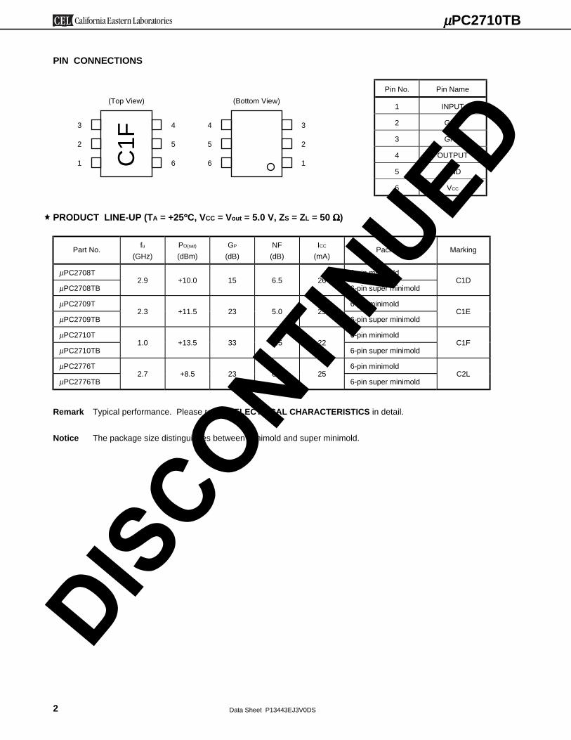
PIN CONNECTIONS
Pin No. Pin Name
1 INPUT
2 GND
3 GND
4 OUTPUT
5 GND
3
2
1
4C
1F(Top View)
5
6
4
5
6
3
(Bottom View)
2
1
6 VCC
PRODUCT LINE-UP (TA = +25°°°°C, VCC = Vout = 5.0 V, ZS = ZL = 50 ΩΩΩΩ)
Part No.fu
(GHz)
PO(sat)
(dBm)
GP
(dB)
NF
(dB)
ICC
(mA)Package Marking
µPC2708T 6-pin minimold
µPC2708TB2.9 +10.0 15 6.5 26
6-pin super minimoldC1D
µPC2709T 6-pin minimold
µPC2709TB2.3 +11.5 23 5.0 25
6-pin super minimoldC1E
µPC2710T 6-pin minimold
µPC2710TB1.0 +13.5 33 3.5 22
6-pin super minimoldC1F
µPC2776T 6-pin minimold
µPC2776TB2.7 +8.5 23 6.0 25
6-pin super minimoldC2L
Remark Typical performance. Please refer to ELECTRICAL CHARACTERISTICS in detail.
Notice The package size distinguishes between minimold and super minimold.
DISCONTIN
UED
Data Sheet P13443EJ3V0DS 3
µµµµPC2710TB
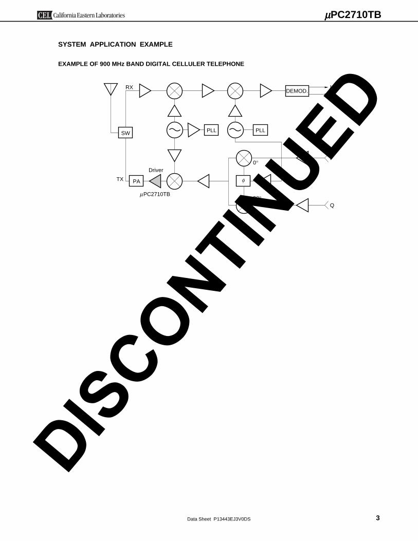
SYSTEM APPLICATION EXAMPLE
EXAMPLE OF 900 MHz BAND DIGITAL CELLULER TELEPHONE
DEMOD.
PLL
I
I
Q
Q
PLL
PATX
PC2710TB
Driver0°
90°
SW
RX
µ
φ
DISCONTIN
UED
Data Sheet P13443EJ3V0DS4
µµµµPC2710TB
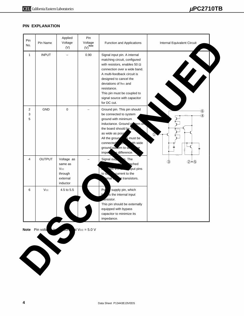
PIN EXPLANATION
Pin
No.Pin Name
Applied
Voltage
(V)
Pin
Voltage
(V)Note
Function and Applications Internal Equivalent Circuit
1 INPUT – 0.90 Signal input pin. A internal
matching circuit, configured
with resistors, enables 50 Ωconnection over a wide band.
A multi-feedback circuit is
designed to cancel the
deviations of hFE and
resistance.
This pin must be coupled to
signal source with capacitor
for DC cut.
2
3
5
GND 0 – Ground pin. This pin should
be connected to system
ground with minimum
inductance. Ground pattern on
the board should be formed
as wide as possible.
All the ground pins must be
connected together with wide
ground pattern to decrease
impedance difference.
4 OUTPUT Voltage as
same as
VCC
through
external
inductor
– Signal output pin. The
inductor must be attached
between VCC and output pins
to supply current to the
internal output transistors.
6 VCC 4.5 to 5.5 – Power supply pin, which
biases the internal input
transistor.
This pin should be externally
equipped with bypass
capacitor to minimize its
impedance.
64
1
23 5
Note Pin voltage is measured at VCC = 5.0 V
DISCONTIN
UED
Data Sheet P13443EJ3V0DS 5
µµµµPC2710TB
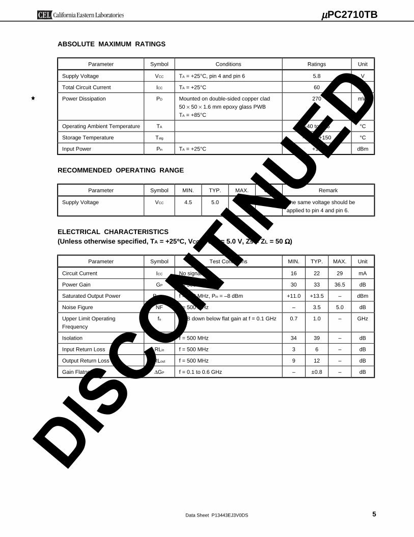
ABSOLUTE MAXIMUM RATINGS
Parameter Symbol Conditions Ratings Unit
Supply Voltage VCC TA = +25°C, pin 4 and pin 6 5.8 V
Total Circuit Current ICC TA = +25°C 60 mA
Power Dissipation PD Mounted on double-sided copper clad
50 × 50 × 1.6 mm epoxy glass PWB
TA = +85°C
270 mW
Operating Ambient Temperature TA −40 to +85 °C
Storage Temperature Tstg −55 to +150 °C
Input Power Pin TA = +25°C +10 dBm
RECOMMENDED OPERATING RANGE
Parameter Symbol MIN. TYP. MAX. Unit Remark
Supply Voltage VCC 4.5 5.0 5.5 V The same voltage should be
applied to pin 4 and pin 6.
ELECTRICAL CHARACTERISTICS(Unless otherwise specified, TA = +25°°°°C, VCC = Vout = 5.0 V, ZS = ZL = 50 ΩΩΩΩ)
Parameter Symbol Test Conditions MIN. TYP. MAX. Unit
Circuit Current ICC No signal 16 22 29 mA
Power Gain GP f = 500 MHz 30 33 36.5 dB
Saturated Output Power PO(sat) f = 500 MHz, Pin = –8 dBm +11.0 +13.5 – dBm
Noise Figure NF f = 500 MHz – 3.5 5.0 dB
Upper Limit Operating
Frequency
fu 3 dB down below flat gain at f = 0.1 GHz 0.7 1.0 – GHz
Isolation ISL f = 500 MHz 34 39 – dB
Input Return Loss RLin f = 500 MHz 3 6 – dB
Output Return Loss RLout f = 500 MHz 9 12 – dB
Gain Flatness ∆GP f = 0.1 to 0.6 GHz – ±0.8 – dB
DISCONTIN
UED
Data Sheet P13443EJ3V0DS6
µµµµPC2710TB
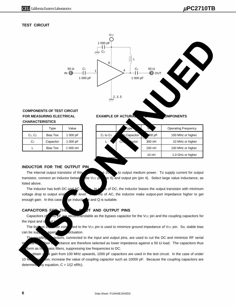
TEST CIRCUIT
VCC
1 000 pF
1 000 pF 1 000 pF
C1 C2
L
4
6
1
2, 3, 5
50 Ω50 ΩOUTIN
C3
COMPONENTS OF TEST CIRCUIT
FOR MEASURING ELECTRICAL
CHARACTERISTICS
EXAMPLE OF ACTURAL APPLICATION COMPONENTS
Type Value Type Value Operating Frequency
C1, C2 Bias Tee 1 000 pF C1 to C3 Chip Capacitor 1 000 pF 100 MHz or higher
C3 Capacitor 1 000 pF 300 nH 10 MHz or higher
L Bias Tee 1 000 nH 100 nH 100 MHz or higher
L Chip Inductor
10 nH 1.0 GHz or higher
INDUCTOR FOR THE OUTPUT PINThe internal output transistor of this IC consumes 20 mA, to output medium power. To supply current for output
transistor, connect an inductor between the VCC pin (pin 6) and output pin (pin 4). Select large value inductance, as
listed above.
The inductor has both DC and AC effects. In terms of DC, the inductor biases the output transistor with minimum
voltage drop to output enable high level. In terms of AC, the inductor make output-port impedance higher to get
enough gain. In this case, large inductance and Q is suitable.
CAPACITORS FOR THE VCC, INPUT AND OUTPUT PINSCapacitors of 1000 pF are recommendable as the bypass capacitor for the VCC pin and the coupling capacitors for
the input and output pins.
The bypass capacitor connected to the VCC pin is used to minimize ground impedance of VCC pin. So, stable bias
can be supplied against VCC fluctuation.
The coupling capacitors, connected to the input and output pins, are used to cut the DC and minimize RF serial
impedance. Their capacitance are therefore selected as lower impedance against a 50 Ω load. The capacitors thus
perform as high pass filters, suppressing low frequencies to DC.
To obtain a flat gain from 100 MHz upwards, 1000 pF capacitors are used in the test circuit. In the case of under
10 MHz operation, increase the value of coupling capacitor such as 10000 pF. Because the coupling capacitors are
determined by equation, C = 1/(2 πRfc).DISCONTIN
UED
Data Sheet P13443EJ3V0DS 7
µµµµPC2710TB
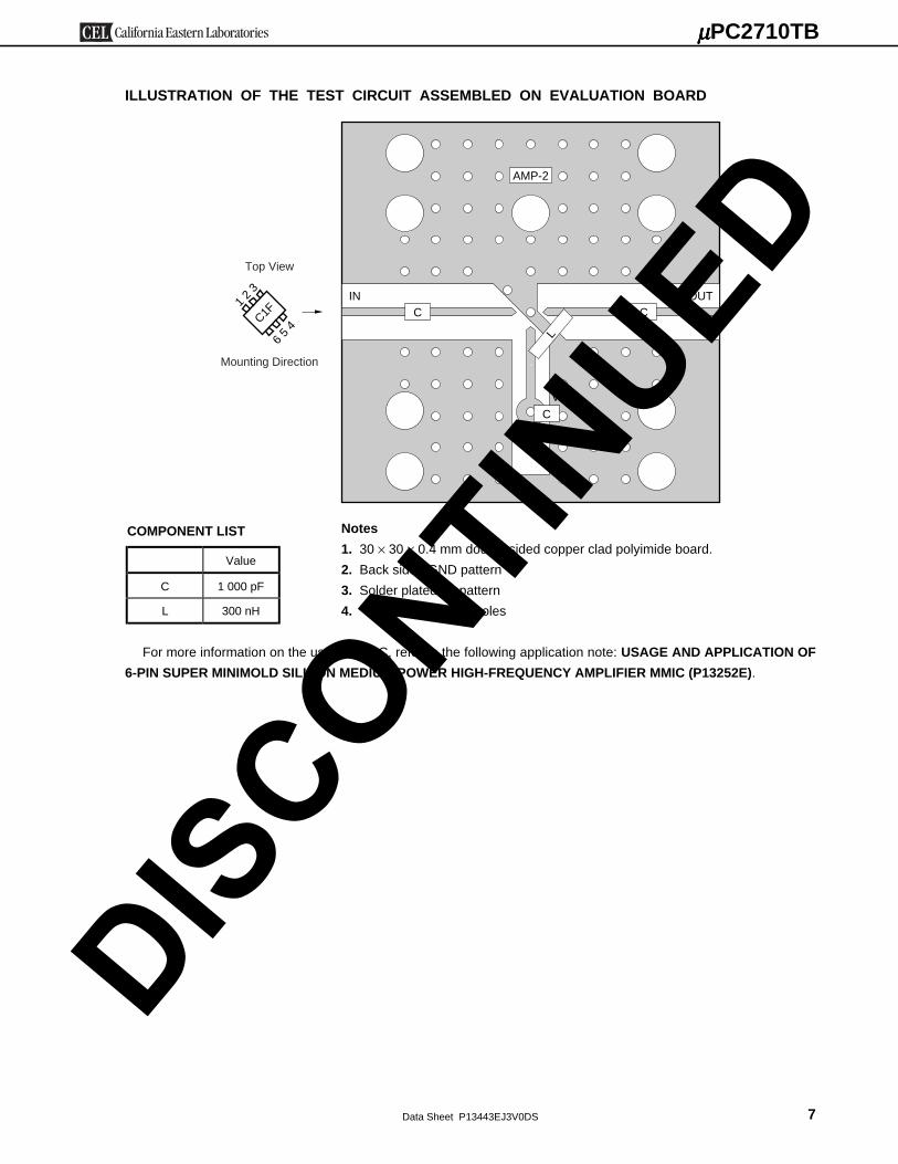
ILLUSTRATION OF THE TEST CIRCUIT ASSEMBLED ON EVALUATION BOARD
C1F3
21
45
6Top View
Mounting Direction
Notes
1.
2.
3.
4.
30 × 30 × 0.4 mm double sided copper clad polyimide board.
Back side: GND pattern
Solder plated on pattern
: Through holes
IN OUT
C
VCC
AMP-2
C C
L
For more information on the use of this IC, refer to the following application note: USAGE AND APPLICATION OF
6-PIN SUPER MINIMOLD SILICON MEDIUM-POWER HIGH-FREQUENCY AMPLIFIER MMIC (P13252E).
COMPONENT LIST
Value
C 1 000 pF
L 300 nH
DISCONTIN
UED
Data Sheet P13443EJ3V0DS8
µµµµPC2710TB
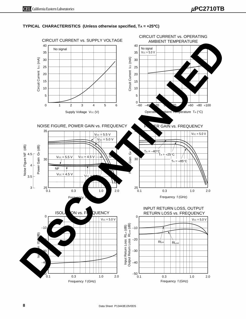
TYPICAL CHARACTERISTICS (Unless otherwise specified, TA = +25°°°°C)
40
30
20
10
0 1 2 3 4 5 6
Circ
uit C
urre
nt I
CC (
mA
)CIRCUIT CURRENT vs. SUPPLY VOLTAGE
Supply Voltage VCC (V)
35
25
15
5
No signal40
30
20
10
00−60 +20 +100
Circ
uit C
urre
nt I
CC (
mA
)
CIRCUIT CURRENT vs. OPERATINGAMBIENT TEMPERATURE
Operating Ambient Temperature TA (°C)
35
25
15
5
−40 −20 +40 +60 +80
No signalVCC = 5.0 V
NOISE FIGURE, POWER GAIN vs. FREQUENCY35
0.3 1.0 2.0
Pow
er G
ain
GP (
dB)
Frequency f (GHz)
250.1
4
4.5
3.5Noi
se F
igur
e N
F (
dB)
30
3
NF
VCC = 4.5 V VCC = 5.0 V
VCC = 5.0 V
GP
VCC = 5.5 V
VCC = 4.5 VVCC = 5.5 V
35
0.3 1.0 2.0
Pow
er G
ain
GP (
dB)
Frequency f (GHz)
250.1
30TA = +85°C
TA = +25°C
VCC = 5.0 V
POWER GAIN vs. FREQUENCY
TA = −40°C
0
−20
−30
−40
0.1 0.3 1.0
Isol
atio
n IS
L (d
B)
Frequency f (GHz)
−50
−10
ISOLATION vs. FREQUENCY
2.0
VCC = 5.0 V
INPUT RETURN LOSS, OUTPUT RETURN LOSS vs. FREQUENCY
−10
−20
1.00.3 2.0
Inpu
t Ret
urn
Loss
RLi
n (d
B)
Out
put R
etur
n Lo
ss R
L out (
dB)
Frequency f (GHz)
−500.1
−30
−40
VCC = 5.0 V0
RLin RLout
DISCONTIN
UED
Data Sheet P13443EJ3V0DS 9
µµµµPC2710TB
OUTPUT POWER vs. INPUT POWER+20
+15
+5
0
−40 0 +10
Out
put P
ower
Pou
t (dB
m)
Input Power Pin (dBm)
−10
−15 −10 −5
+10
−5
−15−20−25−30 +5
VCC = 4.5 V
VCC = 5.5 V
VCC = 5.0 V
f = 0.5 GHz
−35
OUTPUT POWER vs. INPUT POWER+20
+15
+5
0
−40 0 +10
Out
put P
ower
Pou
t (d
Bm
)
Input Power Pin (dBm)
−10
−15 −10 −5
+10
−5
−15−20−25−35 +5
VCC = 5.0 Vf = 0.5 GHz
TA = −40°C
TA = +25°C
TA = +85°C
−30
OUTPUT POWER vs. INPUT POWER+20
+15
+5
0
0 +10
Out
put P
ower
Pou
t (dB
m)
Input Power Pin (dBm)
−10
−15 −10 −5
+10
−5
−15−20−25−30 +5
f = 1.0 GHz
VCC = 4.5 V
VCC = 5.5 V
VCC = 5.0 V
−40 −35
OUTPUT POWER vs. INPUT POWER+20
+15
+5
0
+10
Out
put P
ower
Pou
t (dB
m)
Input Power Pin (dBm)
−10
+10
−5
−15+50
f = 1.0 GHz
VCC = 5.0 V
−15 −10 −5−20−25−30−35−40
f = 0.5 GHz
SATURATED OUTPUT POWER vs.FREQUENCY
+20
+14
+8
0.5 1.0 2.0
Sat
urat
ed O
utpu
t Pow
er P
O (
sat) (
dBm
)
Frequency f (GHz)
+60.1
+18
+16
+12
+10
0.2
Pin = −8 dBm
VCC = 5.0 V
VCC = 4.5 V
VCC = 5.5 V
−60
−50
−40
−30
−10 +103rd
Ord
er In
term
odul
atio
n D
isto
rtio
n IM
3 (d
Bc)
Output Power of Each Tone PO (each) (dBm)
−20
0−10
3RD ORDER INTERMODULATION DISTORTIONvs. OUTPUT POWER OF EACH TONE
+8−8 +6+4+2−6 −4 −2
f1 = 0.500 GHzf2 = 0.502 GHz
VCC = 4.5 V
VCC = 5.0 V
VCC = 5.5 V
DISCONTIN
UED
Data Sheet P13443EJ3V0DS10
µµµµPC2710TB
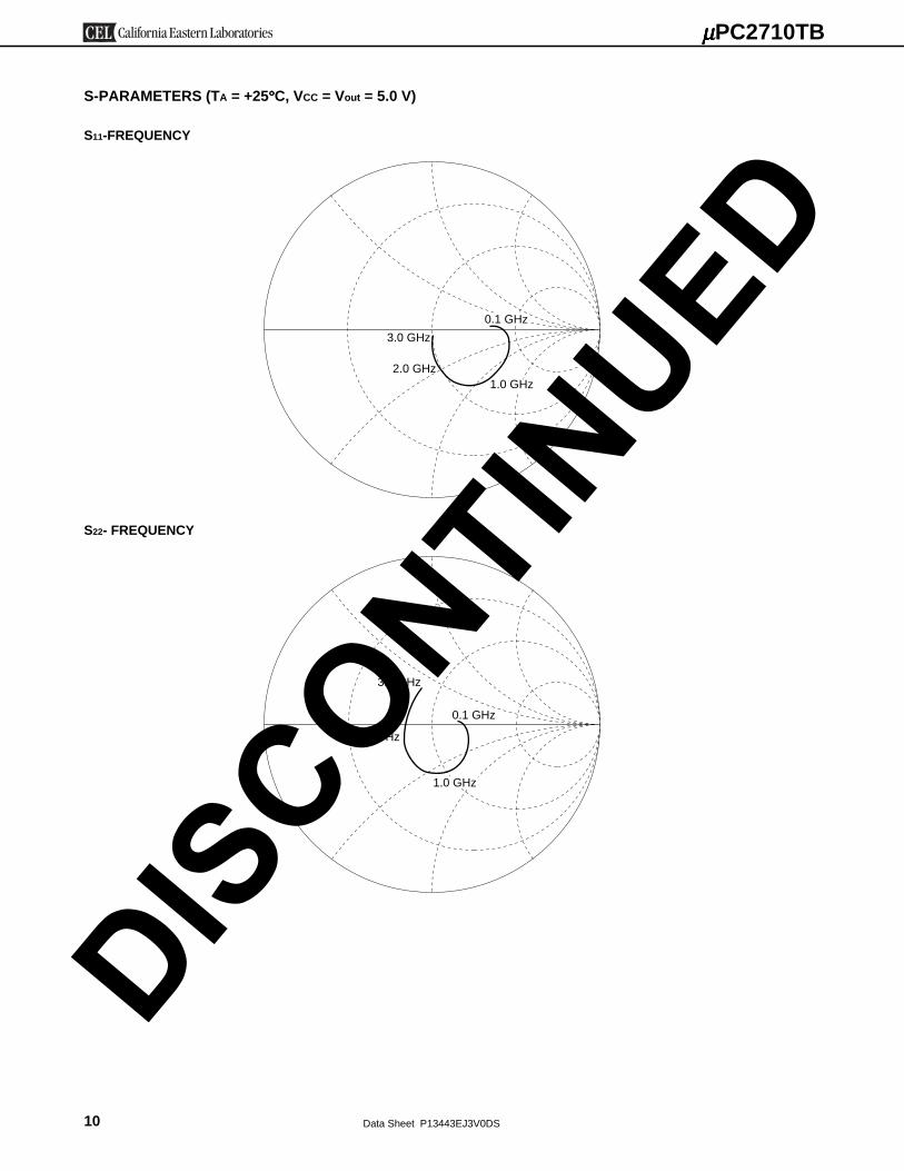
S-PARAMETERS (TA = +25°°°°C, VCC = Vout = 5.0 V)
S11-FREQUENCY
2.0 GHz
3.0 GHz
0.1 GHz
1.0 GHz
S22- FREQUENCY
0.1 GHz
2.0 GHz
3.0 GHz
1.0 GHz
DISCONTIN
UED
Data Sheet P13443EJ3V0DS 11
µµµµPC2710TB
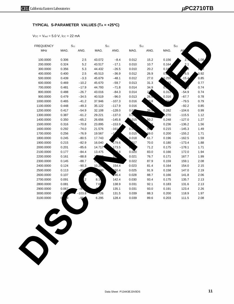
TYPICAL S-PARAMETER VALUES (TA = +25°°°°C)
VCC = Vout = 5.0 V, ICC = 22 mA
FREQUENCY S11 S21 S12 S22 K
MHz MAG. ANG. MAG. ANG. MAG. ANG. MAG. ANG.
100.0000 0.306 2.5 43.072 −8.4 0.012 15.2 0.156 2.7 1.08
200.0000 0.324 5.2 43.517 −17.1 0.010 10.7 0.164 2.1 1.17
300.0000 0.356 5.3 44.432 −26.5 0.010 20.2 0.185 0.3 1.10
400.0000 0.400 2.5 45.513 −36.9 0.012 26.9 0.225 −5.5 0.92
500.0000 0.439 −3.3 45.679 −48.1 0.012 27.0 0.255 −15.4 0.85
600.0000 0.469 −10.2 45.670 −59.7 0.013 31.3 0.283 −27.6 0.77
700.0000 0.481 −17.9 44.793 −71.8 0.014 34.9 0.301 −40.2 0.74
800.0000 0.488 −26.7 43.016 −84.3 0.014 27.9 0.312 −54.9 0.74
900.0000 0.479 −34.5 40.519 −96.0 0.013 26.6 0.316 −67.7 0.78
1000.0000 0.465 −41.2 37.946 −107.3 0.016 30.8 0.311 −79.5 0.79
1100.0000 0.448 −49.3 35.122 −117.9 0.016 26.6 0.307 −92.2 0.85
1200.0000 0.417 −54.9 32.108 −128.0 0.015 39.5 0.282 −104.6 0.99
1300.0000 0.387 −61.2 29.221 −137.0 0.015 39.7 0.270 −115.5 1.12
1400.0000 0.350 −65.2 26.656 −145.8 0.015 50.2 0.248 −127.0 1.27
1500.0000 0.316 −70.8 23.895 −153.9 0.013 50.8 0.236 −136.2 1.56
1600.0000 0.292 −74.0 21.576 −161.6 0.016 56.6 0.215 −145.3 1.49
1700.0000 0.256 −76.9 19.567 −168.1 0.015 69.0 0.200 −155.2 1.71
1800.0000 0.245 −80.5 17.743 −174.4 0.018 61.7 0.196 −162.5 1.59
1900.0000 0.215 −82.9 16.040 179.6 0.017 70.0 0.180 −173.4 1.88
2000.0000 0.201 −85.6 14.717 173.5 0.021 71.2 0.175 −178.1 1.71
2100.0000 0.177 −84.4 13.475 168.8 0.020 83.0 0.166 172.0 1.94
2200.0000 0.161 −88.8 12.327 163.1 0.021 76.7 0.171 167.7 1.99
2300.0000 0.145 −88.7 11.154 158.7 0.022 87.9 0.159 159.1 2.08
2400.0000 0.124 −90.3 10.262 154.4 0.023 81.4 0.164 154.0 2.15
2500.0000 0.113 −89.8 9.490 150.4 0.025 91.9 0.158 147.0 2.19
2600.0000 0.107 −91.9 8.793 146.4 0.028 88.7 0.166 141.8 2.06
2700.0000 0.091 −92.2 8.149 142.4 0.030 93.4 0.175 135.7 2.13
2800.0000 0.081 −94.9 7.652 138.9 0.031 92.1 0.183 131.6 2.13
2900.0000 0.067 −97.4 7.134 135.1 0.031 93.0 0.191 123.4 2.26
3000.0000 0.055 −103.8 6.726 131.5 0.039 88.3 0.200 118.9 1.97
3100.0000 0.039 −95.6 6.295 128.4 0.039 89.6 0.203 111.5 2.08
DISCONTIN
UED
Data Sheet P13443EJ3V0DS12
µµµµPC2710TB
PACKAGE DIMENSIONS
6-PIN SUPER MINIMOLD (UNIT: mm)
0.9±
0.1
0.7
0 to
0.1 0.
15+
0.1
–0
.05
2.0±
0.2
1.3 0.
650.
65
0.2+
0.1
–0
.05
2.1±0.1
1.25±0.1
0.1 MIN.
DISCONTIN
UED
Data Sheet P13443EJ3V0DS 13
µµµµPC2710TB
NOTES ON CORRECT USE(1) Observe precautions for handling because of electro-static sensitive devices.
(2) Form a ground pattern as widely as possible to minimize ground impedance (to prevent undesired oscillation).
All the ground pins must be connected together with wide ground pattern to decrease impedance difference.
(3) The bypass capacitor should be attached to VCC line.
(4) The inductor must be attached between VCC and output pins. The inductance value should be determined in
accordance with desired frequency.
(5) The DC cut capacitor must be attached to input pin and output pin.
RECOMMENDED SOLDERING CONDITIONSThis product should be soldered under the following recommended conditions.
Soldering Method Soldering Conditions Recommended Condition Symbol
Infrared Reflow Package peak temperature: 235°C or below
Time: 30 seconds or less (at 210°C)
Count: 3, Exposure limit: NoneNote
IR35-00-3
VPS Package peak temperature: 215°C or below
Time: 40 seconds or less (at 200°C)
Count: 3, Exposure limit: NoneNote
VP15-00-3
Wave Soldering Soldering bath temperature: 260°C or below
Time: 10 seconds or less
Count: 1, Exposure limit: NoneNote
WS60-00-1
Partial Heating Pin temperature: 300°C or below
Time: 3 seconds or less (per side of device)
Exposure limit: NoneNote
–
Note After opening the dry pack, keep it in a place below 25°C and 65% RH for the allowable storage period.
Caution Do not use different soldering methods together (except for partial heating).
For details of recommended soldering conditions for surface mounting, refer to information document
SEMICONDUCTOR DEVICE MOUNTING TECHNOLOGY MANUAL (C10535E).
DISCONTIN
UED

NOTICE
1. Descriptions of circuits, software and other related information in this document are provided only to illustrate the operation of semiconductor products andapplication examples. You are fully responsible for the incorporation of these circuits, software, and information in the design of your equipment. CaliforniaEastern Laboratories and Renesas Electronics assumes no responsibility for any losses incurred by you or third parties arising from the use of these circuits, software, or information.
2. California Eastern Laboratories has used reasonable care in preparing the information included in this document, but California Eastern Laboratories doesnot warrant that such information is error free. California Eastern Laboratories and Renesas Electronics assumes no liability whatsoever for any damagesincurred by you resulting from errors in or omissions from the information included herein.
3. California Eastern Laboratories and Renesas Electronics do not assume any liability for infringement of patents, copyrights, or other intellectual propertyrights of third parties by or arising from the use of Renesas Electronics products or technical information described in this document. No license, express,implied or otherwise, is granted hereby under any patents, copyrights or other intellectual property rights of California Eastern Laboratories or RenesasElectronics or others.
4. You should not alter, modify, copy, or otherwise misappropriate any Renesas Electronics product, whether in whole or in part. California EasternLaboratories and Renesas Electronics assume no responsibility for any losses incurred by you or third parties arising from such alteration, modification, copyor otherwise misappropriation of Renesas Electronics product.
5. Renesas Electronics products are classified according to the following two quality grades: “Standard” and “High Quality”. The recommended applicationsfor each Renesas Electronics product depends on the product’s quality grade, as indicated below. “Standard”: Computers; office equipment; communicationsequipment; test and measurement equipment; audio and visual equipment; home electronic appliances; machine tools; personal electronic equipment; and industrial robots etc. “High Quality”: Transportation equipment (automobiles, trains, ships, etc.); traffic control systems; anti-disaster systems; anti-crime systems; and safety equipment etc. Renesas Electronics products are neither intended nor authorized for use in products or systems that may pose a direct threat to human life or bodily injury (artificial life support devices or systems, surgical implantations etc.), or may cause serious property damages (nuclearreactor control systems, military equipment etc.). You must check the quality grade of each Renesas Electronics product before using it in a particularapplication. You may not use any Renesas Electronics product for any application for which it is not intended. California Eastern Laboratories and RenesasElectronics shall not be in any way liable for any damages or losses incurred by you or third parties arising from the use of any Renesas Electronics productfor which the product is not intended by California Eastern Laboratories or Renesas Electronics.
6. You should use the Renesas Electronics products described in this document within the range specified by California Eastern Laboratories, especially with respect to the maximum rating, operating supply voltage range, movement power voltage range, heat radiation characteristics, installation and other productcharacteristics. California Eastern Laboratories shall have no liability for malfunctions or damages arising out of the use of Renesas Electronics productsbeyond such specified ranges.
7. Although Renesas Electronics endeavors to improve the quality and reliability of its products, semiconductor products have specific characteristics such as the occurrence of failure at a certain rate and malfunctions under certain use conditions. Further, Renesas Electronics products are not subject to radiationresistance design. Please be sure to implement safety measures to guard them against the possibility of physical injury, and injury or damage caused by fire in the event of the failure of a Renesas Electronics product, such as safety design for hardware and software including but not limited to redundancy, fire control and malfunction prevention, appropriate treatment for aging degradation or any other appropriate measures. Because the evaluation ofmicrocomputer software alone is very difficult, please evaluate the safety of the final products or systems manufactured by you.
8. Please contact a California Eastern Laboratories sales office for details as to environmental matters such as the environmental compatibility of each Renesas Electronics product. Please use Renesas Electronics products in compliance with all applicable laws and regulations that regulate the inclusion or use of controlled substances, including without limitation, the EU RoHS Directive. California Eastern Laboratories and Renesas Electronics assume no liability for damages or losses occurring as a result of your noncompliance with applicable laws and regulations.
9. Renesas Electronics products and technology may not be used for or incorporated into any products or systems whose manufacture, use, or sale is prohibited under any applicable domestic or foreign laws or regulations. You should not use Renesas Electronics products or technology described in this document for any purpose relating to military applications or use by the military, including but not limited to the development of weapons of mass destruction. Whenexporting the Renesas Electronics products or technology described in this document, you should comply with the applicable export control laws and regulations and follow the procedures required by such laws and regulations.
10. It is the responsibility of the buyer or distributor of California Eastern Laboratories, who distributes, disposes of, or otherwise places the Renesas Electronicsproduct with a third party, to notify such third party in advance of the contents and conditions set forth in this document, California Eastern Laboratories andRenesas Electronics assume no responsibility for any losses incurred by you or third parties as a result of unauthorized use of Renesas Electronics products.
11. This document may not be reproduced or duplicated in any form, in whole or in part, without prior written consent of California Eastern Laboratories.12. Please contact a California Eastern Laboratories sales office if you have any questions regarding the information contained in this document or Renesas
Electronics products, or if you have any other inquiries.
NOTE 1: “Renesas Electronics” as used in this document means Renesas Electronics Corporation and also includes its majority-owned subsidiaries.NOTE 2: “Renesas Electronics product(s)” means any product developed or manufactured by or for Renesas Electronics.NOTE 3: Products and product information are subject to change without notice.
CEL Headquarters • 4590 Patrick Henry Drive, Santa Clara, CA 95054 • Phone (408) 919-2500 • www.cel.com
For a complete list of sales offices, representatives and distributors,Please visit our website: www.cel.com/contactusDISCONTIN
UED