Embed Size (px)
Citation preview

1P/N:PM1149 REV. 2.6, APR. 11, 2012
MX29LV040C4M-BIT [512K x 8] CMOS SINGLE VOLTAGE 3V ONLY EQUAL SECTOR FLASH MEMORY
FEATURES
• Extendedsingle-supplyvoltagerange2.7Vto3.6V• 524,288x8only• Singlepowersupplyoperation -3.0Vonlyoperationforread,eraseandprogramoperation• Fully compatible with MX29LV040 device• Fastaccesstime:55Q/70/90ns• Lowpowerconsumption -30mAmaximumactivecurrent -0.2uAtypicalstandbycurrent• Commandregisterarchitecture -8equalsectorof64K-Byteeach -ByteProgramming(9ustypical) -SectorErase(Sectorstructure64K-Bytex8)• AutoErase(chip§or)andAutoProgram -AutomaticallyeraseanycombinationofsectorswithEraseSuspendcapability -Automaticallyprogramandverifydataatspecifiedaddress• Erasesuspend/EraseResume -Suspendssectoreraseoperationtoreaddatafrom,orprogramdatato,anysectorthatisnotbeingerased,thenresumestheerase
• StatusReply -Data#Polling&Togglebitfordetectionofprogramanderaseoperationcompletion• Sectorprotection -Hardwaremethodtodisableanycombinationofsectorsfromprogramoreraseoperations -Anycombinationofsectorscanbeerasedwitherasesuspend/resumefunction• CFI(CommonFlashInterface)compliant -Flashdeviceparametersstoredonthedeviceandprovidethehostsystemtoaccess• 100,000minimumerase/programcycles• Latch-upprotectedto100mAfrom-1VtoVCC+1V• Packagetype: -32-pinPLCC -32-pinTSOP(8mmx20mm,8mmx14mm) - All devices are RoHS Compliant

2P/N:PM1149 REV. 2.6, APR. 11, 2012
MX29LV040C
PIN CONFIGURATIONS
32 PLCC
32 TSOP (Standard Type) (8mm x 20mm)
PIN DESCRIPTION
A11A9A8
A13A14A17
WE#VCCA18A16A15A12
A7A6A5A4
12345678910111213141516
OE#A10CE#Q7Q6Q5Q4Q3GNDQ2Q1Q0A0A1A2A3
32313029282726252423222120191817
MX29LV040C
145
9
1314 17 20
21
25
2932 30
A14
A13
A8
A9
A11
OE#
A10
CE#
Q7
A7
A6
A5
A4
A3
A2
A1
A0
Q0
Q1
Q2
GN
D Q3
Q4
Q5
Q6
A12
A15
A16
A18
VC
C
WE
#
A17
MX29LV040C
SYMBOL PIN NAMEA0~A18 AddressInputQ0~Q7 DataInput/OutputCE# ChipEnableInputWE# WriteEnableInputOE# OutputEnableInputGND GroundPinVCC +3.0Vsinglepowersupply
32 TSOP (8mm x 14mm)
A11A9A8
A13A14A17
WE#VCCA18A16A15A12
A7A6A5A4
12345678910111213141516
OE#A10CE#Q7Q6Q5Q4Q3GNDQ2Q1Q0A0A1A2A3
32313029282726252423222120191817
MX29LV040C

3P/N:PM1149 REV. 2.6, APR. 11, 2012
MX29LV040C
BLOCK DIAGRAM
CONTROLINPUTLOGIC
PROGRAM/ERASEHIGH VOLTAGE
WRITESTATE
MACHINE(WSM)
STATEREGISTER
FLASHARRAY
X-D
EC
OD
ER
ADDRESS
LATCH
AND
BUFFER Y-PASS GATE
Y-DE
CO
DE
RARRAY
SOURCEHV COMMAND
DATADECODER
COMMANDDATA LATCH
I/O BUFFER
PGMDATA
HV
PROGRAMDATA LATCH
SENSEAMPLIFIER
Q0-Q7
A0-A18
CE#OE#WE#

4P/N:PM1149 REV. 2.6, APR. 11, 2012
MX29LV040C
Table 1. SECTOR (GROUP) STRUCTURE
Note:Allsectorsare64Kbytesinsize.
Sector A18 A17 A16 Address RangeSA0 0 0 0 00000h-0FFFFhSA1 0 0 1 10000h-1FFFFhSA2 0 1 0 20000h-2FFFFhSA3 0 1 1 30000h-3FFFFhSA4 1 0 0 40000h-4FFFFhSA5 1 0 1 50000h-5FFFFhSA6 1 1 0 60000h-6FFFFhSA7 1 1 1 70000h-7FFFFh

5P/N:PM1149 REV. 2.6, APR. 11, 2012
MX29LV040C
Table 2-1. BUS OPERATION
Table 2-2. BUS OPERATION
Notes:1.Sectorunprotectedcode:00h.Sectorprotectedcode:01h.2.AM:MSBofaddress.3.Sectoraddresses:A18~A16.4.Vhvis11.5Vto12.5V.5.Xmeansdon'tcare.
Operation CE# OE# WE# Address Q7~Q0ReadMode L L H AIN DOUTWrite L H L AIN DINStandbyMode Vcc±0.3V X X X High-ZOutputDisable L H H X High-Z
Operation CE# OE# WE# A0 A1 A6 A9 Q7~Q0ReadSiliconIDManufacturesCode L L H L L X Vhv C2H
ReadSiliconIDDeviceCode L L H H L X Vhv 4FH
SectorProtect L Vhv L X X L Vhv XChipUnprotected L Vhv L X X H Vhv XSectorProtectVerify L L H X H X Vhv Code(1)

6P/N:PM1149 REV. 2.6, APR. 11, 2012
MX29LV040C
WRITE COMMANDS/COMMAND SEQUENCES
Towriteacommandtothedevice,systemmustdriveWE#andCE#toVil,andOE#toVih.Inacommandcycle,alladdressare latchedat the later fallingedgeofCE#andWE#,andalldataare latchedat theearlier risingedgeofCE#andWE#.
Figure1illustratestheACtimingwaveformofawritecommand,andTable3definesallthevalidcommandsetsofthedevice.Systemisnotallowedtowriteinvalidcommandsnotdefinedinthisdatasheet.Writinganinvalidcommandwillbringthedevicetoanundefinedstate.
REQUIREMENTS FOR READING ARRAY DATA
Readarrayactionistoreadthedatastoredinthearray.Whilethememorydeviceisinpowereduporhasbeenreset,itwillautomaticallyenterthestatusofreadarray.Ifthemicroprocessorwantstoreadthedatastoredinthearray,ithastodriveCE#(deviceenablecontrolpin)andOE#(Outputcontrolpin)asVil,andinputtheaddressofthedatatobereadintoaddresspinatthesametime.Afteraperiodofreadcycle(TceorTaa),thedatabeingreadoutwillbedisplayedonoutputpinformicroprocessortoaccess.IfCE#orOE#isVih,theoutputwillbeintri-state,andtherewillbenodatadisplayedonoutputpinatall.
Afterthememorydevicecompletesembeddedoperation(automaticEraseorProgram),itwillautomaticallyre-turntothestatusofreadarray,andthedevicecanreadthedatainanyaddressinthearray.Intheprocessoferasing,ifthedevicereceivestheErasesuspendcommand,eraseoperationwillbestoppedtemporarilyafteraperiodoftimenomorethanTready1andthedevicewillreturntothestatusofreadarray.Atthistime,thedevicecanreadthedatastoredinanyaddressexceptthesectorbeingerasedinthearray.Inthestatusoferasesus-pend,ifuserwantstoreadthedatainthesectorsbeingerased,thedevicewilloutputstatusdataontotheout-put.Similarly,ifprogramcommandisissuedaftererasesuspend,afterprogramoperationiscompleted,systemcanstillreadarraydatainanyaddressexceptthesectorstobeerased.Thedeviceneedsto issueresetcommandtoenablereadarrayoperationagaininordertoarbitrarilyreadthedatainthearrayinthefollowingtwosituations:
1.Inprogramoreraseoperation,theprogrammingorerasingfailurecausesQ5togohigh.
2.ThedeviceisinautoselectmodeorCFImode.
In the twosituationsabove, if resetcommand isnot issued, thedevice isnot in readarraymodeandsystemmustissueresetcommandbeforereadingarraydata.
7P/N:PM1149 REV. 2.6, APR. 11, 2012
MX29LV040C
SECTOR PROTECT OPERATION
Whenasectorisprotected,programoreraseoperationwillbedisabledonthatprotectedsector.MX29LV040Cprovidesamethodsforsectorprotection.
ThemethodisassertingVhvonA9andOE#pins,withA6andCE#atVil.TheprotectionoperationbeginsatthefallingedgeofWE#andterminatesattherisingedge.ContactMacronixfordetails.
CHIP UNPROTECT OPERATION
MX29LV040Cprovidesonemethodsforchipunprotect.Thechipunprotectoperationunprotectsallsectorswith-inthedevice.It isrecommendedtoprotectallsectorsbeforeactivatingchipunprotectmode.Allsectorgroupsareunprotectedwhenshippedfromthefactory.
ThemethodisassertingVhvonA9andOE#pins,withA6atVihandCE#atVil(seeTable2).Theunprotectop-erationbeginsatthefallingedgeofWE#andterminatesattherisingedge.ContactMacronixfordetails.
AUTOMATIC SELECT OPERATION
WhenthedeviceisinReadarraymode,erase-suspendedreadarraymodeorCFImode,usercanissuereadsiliconIDcommandtoenterreadsiliconIDmode.AfterenteringreadsiliconIDmode,usercanqueryseveralsiliconIDscontinuouslyanddoesnotneedtoissuereadsiliconIDmodeagain.WhenA0isLow,devicewillout-putMacronixManufactureIDC2.WhenA0ishigh,devicewilloutputDeviceID.InreadsiliconIDmode,issuingresetcommandwillresetdevicebacktoreadarraymodeorerase-suspendedreadarraymode.
AnotherwaytoenterreadsiliconIDistoapplyhighvoltageonA9pinwithCE#,OE#,A6andA1atVil.WhilethehighvoltageofA9pinisdischarged,devicewillautomaticallyleavereadsiliconIDmodeandgobacktoreadarraymodeorerase-suspendedreadarraymode.WhenA0isLow,devicewilloutputMacronixManufactureIDC2.WhenA0ishigh,devicewilloutputDeviceID.
VERIFY SECTOR PROTECT STATUS OPERATION
MX29LV040CprovideshardwaresectorprotectionagainstProgramandEraseoperationforprotectedsectors.ThesectorprotectstatuscanbereadthroughSectorProtectVerifycommand.ThismethodrequiresVhvonA9pin,VihonWE#andA1pins,VilonCE#,OE#,A6andA0pins,andsectoraddressonA16toA18pins.Ifthereadoutdatais01H,thedesignatedsectorisprotected.Oppositely,ifthereadoutdatais00H,thedesignatedsectorisnotprotected.
DATA PROTECTION
Toavoidaccidentalerasureorprogrammingofthedevice,thedeviceisautomaticallyresettoreadarraymodeduringpowerup.Besides,onlyaftersuccessfulcompletionofthespecifiedcommandsetswillthedevicebeginitseraseorprogramoperation.
Otherfeaturestoprotectthedatafromaccidentalalternationaredescribedasfollowed.

8P/N:PM1149 REV. 2.6, APR. 11, 2012
MX29LV040C
LOW VCC WRITE INHIBIT
ThedevicerefusestoacceptanywritecommandwhenVccislessthan1.4V.Thispreventsdatafromspuriouslyaltered.ThedeviceautomaticallyresetsitselfwhenVccislowerthan1.4VandwritecyclesareignoreduntilVccisgreaterthan1.4V.SystemmustprovidepropersignalsoncontrolpinsafterVccislargerthan1.4Vtoavoidunintentionalprogramoreraseoperation
WRITE PULSE "GLITCH" PROTECTION
CE#,WE#,OE#pulsesshorter than5nsaretreatedasglitchesandwillnotberegardedasaneffectivewritecycle.
LOGICAL INHIBIT
AvalidwritecyclerequiresbothCE#andWE#atVilwithOE#atVih.WritecycleisignoredwheneitherCE#atVih,WE#aVih,orOE#atVil.
POWER-UP SEQUENCE
Uponpowerup,MX29LV040Cisplacedinreadarraymode.Furthermore,programoreraseoperationwillbeginonlyaftersuccessfulcompletionofspecifiedcommandsequences.
POWER-UP WRITE INHIBIT
WhenWE#,CE#isheldatVilandOE#isheldatVihduringpowerup,thedeviceignoresthefirstcommandontherisingedgeofWE#.
POWER SUPPLY DECOUPLING
A0.1uFcapacitorshouldbeconnectedbetweentheVccandGNDtoreducethenoiseeffect.
9P/N:PM1149 REV. 2.6, APR. 11, 2012
MX29LV040C
TABLE 3. MX29LV040C COMMAND DEFINITIONS
Notes:1.Itisnotallowedtoadoptanyothercodewhichisnotintheabovecommanddefinitiontable.
Command ReadMode
ResetMode
AutomaticSelect
Program ChipErase
SectorErase CFIRead Erase
SuspendEraseResumeSilicon
IDDeviceID
SectorProtectVerify
1stBusCyc
Addr Addr XXX 555 555 555 555 555 555 AA XXX XXXData Data F0 AA AA AA AA AA AA 98 B0 30
2ndBusCyc
Addr 2AA 2AA 2AA 2AA 2AA 2AAData 55 55 55 55 55 55
3rdBusCyc
Addr 555 555 555 555 555 555Data 90 90 90 A0 80 80
4thBusCyc
Addr X00 X01 (Sector)X02 Addr 555 555
Data C2 4F 00/01 Data AA AA5thBusCyc
Addr 2AA 2AAData 55 55
6thBusCyc
Addr 555 SectorData 10 30

10P/N:PM1149 REV. 2.6, APR. 11, 2012
MX29LV040C
RESET
Inthefollowingsituations,executingresetcommandwillresetdevicebacktoreadarraymode:• Amongerasecommandsequence(beforethefullcommandsetiscompleted)• Sectorerasetime-outperiod• Erasefail(whileQ5ishigh)• Amongprogramcommandsequence(beforethefullcommandset iscompleted,erase-suspendedprogramincluded)
• Programfail(whileQ5ishigh,anderase-suspendedprogramfailisincluded)• ReadsiliconIDmode• Sectorprotectverify• CFImode
Whiledeviceisatthestatusofprogramfailorerasefail(Q5ishigh),usermustissueresetcommandtoresetdevicebacktoreadarraymode.WhilethedeviceisinreadsiliconIDmode,sectorprotectverifyorCFImode,usermustissueresetcommandtoresetdevicebacktoreadarraymode.
Whenthedeviceisintheprogressofprogramming(notprogramfail)orerasing(noterasefail),devicewillig-noreresetcommand.

11P/N:PM1149 REV. 2.6, APR. 11, 2012
MX29LV040C
AUTOMATIC PROGRAMMING
TheMX29LV040CcanprovidetheuserprogramfunctionbytheformofByte-Mode.AslongastheusersentertherightcycledefinedintheTable.3(including2unlockcyclesandA0H),anydatauserinputswillautomaticallybeprogrammedintothearray.
Once theprogram function is executed, the internalwrite state controllerwill automatically execute thealgo-rithmsand timingsnecessary forprogramandverification,which includesgeneratingsuitableprogrampulse,verifyingwhetherthethresholdvoltageoftheprogrammedcellishighenoughandrepeatingtheprogrampulseifanyofthecellsdoesnotpassverification.Meanwhile,theinternalcontrolwillprohibittheprogrammingtocellsthatpassverificationwhiletheothercellsfailinverificationinordertoavoidover-programming.Withtheinternalwritestatecontroller,thedevicerequirestheusertowritetheprogramcommandanddataonly.
Programmingwillonlychangethebitstatusfrom"1"to"0".Thatistosay,itisimpossibletoconvertthebitstatusfrom"0"to"1"byprogramming.Meanwhile,theinternalwriteverificationonlydetectstheerrorsofthe"1"thatisnotsuccessfullyprogrammedto"0".
Anycommandwrittentothedeviceduringprogrammingwillbeignoredexcepthardwarereset,whichwilltermi-natetheprogramoperationafteraperiodoftimenomorethanTready1.Whentheembeddedprogramalgorithmiscompleteortheprogramoperationisterminatedbyhardwarereset,thedevicewillreturntothereadingarraydatamode.
ThetypicalchipprogramtimeatroomtemperatureoftheMX29LV040Cislessthan4.5seconds.
Whentheembeddedprogramoperationisongoing,usercanconfirmiftheembeddedoperationisfinishedornotbythefollowingmethods:
*1:Thestatus"inprogress"meansbothprogrammodeanderase-suspendedprogrammode.*2:Whenanattemptismadetoprogramaprotectedsector,Q7willoutputitscomplementdataorQ6continuestotoggleforabout1usorlessandthedevicereturnstoreadarraystatewithoutprogramingthedatainthepro-tectedsector.
Status Q7 Q6 Q5Inprogress*1 Q7# Toggling 0Finished Q7 Stoptoggling 0
Exceedtimelimit Q7# Toggling 1
12P/N:PM1149 REV. 2.6, APR. 11, 2012
MX29LV040C
SECTOR ERASE
SectorEraseistoeraseallthedatainasectorwith"1"and"0"asall"1".Itrequiressixcommandcyclestois-sue.Thefirsttwocyclesare"unlockcycles",thethirdoneisaconfigurationcycle,thefourthandfiftharealso"unlockcycles"andthesixthcycleisthesectorerasecommand.Afterthesectorerasecommandsequenceisissued, there isa time-outperiodof50uscounted internally.During the time-outperiod,additional sectorad-dressandsectorerasecommandcanbewrittenmultiply.Onceuserentersanothersectorerasecommand,thetime-outperiodof50usisrecounted.Ifuserentersanycommandotherthansectoreraseorerasesuspenddur-ingtime-outperiod,theerasecommandwouldbeabortedandthedeviceisresettoreadarraycondition.Thenumberofsectorscouldbefromonesectortoallsectors.Aftertime-outperiodpassingby,additionalerasecom-mandisnotacceptedanderaseembeddedoperationbegins.
Duringsectorerasing,allcommandswillnotbeacceptedexcepthardwareresetanderasesuspendandusercancheckthestatusaschiperase.
Whentheembeddederaseoperationisongoing,usercanconfirmiftheembeddedoperationisfinishedornotbythefollowingmethods:
CHIP ERASE
ChipEraseistoeraseallthedatawith"1"and"0"asall"1".Itneeds6cyclestowritetheactionin,andthefirsttwocyclesare"unlock"cycles,thethirdoneisaconfigurationcycle,thefourthandfiftharealso"unlock"cycles,andthesixthcycleisthechiperaseoperation.
Duringchiperasing,allthecommandswillnotbeacceptedexcepthardwareresetortheworkingvoltageistoolowthatchiperasewillbeinterrupted.AfterChipErase,thechipwillreturntothestateofReadArray.
Whentheembeddedchiperaseoperationisongoing,usercanconfirmiftheembeddedoperationisfinishedornotbythefollowingmethods:
*1:ThestatusQ3isthetime-outperiodindicator.WhenQ3=0,thedeviceisintime-outperiodandisacceptibletoanothersectoraddresstobeerased.WhenQ3=1,thedeviceisineraseoperationandonlyerasesuspendisvalid.*2:Whenanattempt ismadetoeraseaprotectedsector,Q7willoutput itscomplementdataorQ6continuestotogglefor100usorlessandthedevicereturnedtoreadarraystatuswithouterasingthedataintheprotectedsector.
Status Q7 Q6 Q5 Q2Inprogress 0 Toggling 0 TogglingFinished 1 Stoptoggling 0 1
Exceedtimelimit 0 Toggling 1 Toggling
Status Q7 Q6 Q5 Q3 Q2Time-outperiod 0 Toggling 0 0 TogglingInprogress 0 Toggling 0 1 TogglingFinished 1 Stoptoggling 0 1 1
Exceedtimelimit 0 Toggling 1 1 Toggling

13P/N:PM1149 REV. 2.6, APR. 11, 2012
MX29LV040C
When thedevicehassuspendederasing,user canexecute thecommandsetsexcept sectoreraseandchiperase,suchasreadsiliconID,sectorprotectverify,program,CFIqueryanderaseresume.
SECTOR ERASE RESUME
Sectoreraseresumecommandisvalidonlywhenthedeviceisinerasesuspendstate.Aftereraseresume,usercanissueanothererasesuspendcommand,butthereshouldbea400uSintervalbetweeneraseresumeandthenexterasesuspend.Ifuserissueinfinitesuspend-resumeloop,orsuspend-resumeexceeds1024times,thetimeforerasingwillincrease.
SECTOR ERASE SUSPEND
Duringsectorerasure,sectorerasesuspendistheonlyvalidcommand.Ifuserissueerasesuspendcommandinthetime-outperiodofsectorerasure,devicetime-outperiodwillbeover immediatelyandthedevicewillgobacktoerase-suspendedreadarraymode.Ifuserissueerasesuspendcommandduringthesectoreraseisbe-ingoperated,devicewillsuspendtheongoingeraseoperation,andaftertheTready1(<=20us)suspendfinishesandthedevicewillentererase-suspendedreadarraymode.Usercanjudgeifthedevicehasfinishederasesus-pendthroughQ6,Q7,andRY/BY#.
Afterdevicehasenterederase-suspendedreadarraymode,usercanreadothersectorsnotaterasesuspendbythespeedofTaa;whilereadingthesectorinerase-suspendmode,devicewilloutputitsstatus.UsercanuseQ6andQ2tojudgethesectoriserasingortheeraseissuspended.
Status Q7 Q6 Q5 Q3 Q2Erasesuspendreadinerasesuspendedsector 1 Notoggle 0 N/A ToggleErasesuspendreadinnon-erasesuspendedsector Data Data Data Data DataErasesuspendprograminnon-erasesuspendedsector Q7# Toggle 0 N/A N/A

14P/N:PM1149 REV. 2.6, APR. 11, 2012
MX29LV040C
Table 4-1. CFI mode: Identification Data Values(Allvaluesinthesetablesareinhexadecimal)
QUERY COMMAND AND COMMON FLASH INTERFACE (CFI) MODE
MX29LV040CfeaturesCFImode.Hostsystemcanretrievetheoperatingcharacteristics,structureandvendor-specified information suchas identifying information,memory size, byte configuration, operating voltagesandtiminginformationofthisdevicebyCFImode.If thesystemwritestheCFIQuerycommand"98h", toaddress"55h"/"AAh",thedevicewillentertheCFIQueryMode,anytimethedeviceisreadytoreadarraydata.Thesys-temcanreadCFIinformationattheaddressesgiveninTable4.
OnceuserentersCFIquerymode,usercannotissueanyothercommandsexceptresetcommand.TheresetcommandisrequiredtoexitCFImodeandgobacktothemodebeforeenteringCFI.ThesystemcanwritetheCFIQuerycommandonlywhenthedeviceisinreadmode,erasesuspend,standbymodeorautomaticselectmode.
Table 4-2. CFI Mode: System Interface Data Values
Description Address (h) (Byte Mode) Data (h)
Vccsupplyminimumprogram/erasevoltage 1B 0027Vccsupplymaximumprogram/erasevoltage 1C 0036VPPsupplyminimumprogram/erasevoltage 1D 0000VPPsupplymaximumprogram/erasevoltage 1E 0000Typicaltimeoutpersingleword/bytewrite,2nus 1F 0004Typicaltimeoutformaximum-sizebufferwrite,2nus 20 0000Typicaltimeoutperindividualblockerase,2nms 21 000ATypicaltimeoutforfullchiperase,2nms 22 0000Maximumtimeoutforword/bytewrite,2ntimestypical 23 0005Maximumtimeoutforbufferwrite,2ntimestypical 24 0000Maximumtimeoutperindividualblockerase,2ntimestypical 25 0004Maximumtimeoutforchiperase,2ntimestypical 26 0000
Description Address (h) (Byte Mode) Data (h)
Query-uniqueASCIIstring"QRY"10 005111 005212 0059
PrimaryvendorcommandsetandcontrolinterfaceIDcode 13 000214 0000
Addressforprimaryalgorithmextendedquerytable 15 004016 0000
AlternatevendorcommandsetandcontrolinterfaceIDcode(none) 17 000018 0000
Addressforalternatealgorithmextendedquerytable(none) 19 00001A 0000

15P/N:PM1149 REV. 2.6, APR. 11, 2012
MX29LV040C
Table 4-3. CFI Mode: Device Geometry Data Values
Description Address (h) (Byte Mode) Data (h)
Devicesize=2ninnumberofbytes 27 0013
Flashdeviceinterfacedescription(02=asynchronousx8/x16) 28 000029 0000
Maximumnumberofbytesinbufferwrite=2n(notsupport) 2A 00002B 0000
Numberoferaseregionswithindevice 2C 0001
IndexforEraseBankArea1
2D 00072E 00002F 000030 0001
IndexforEraseBankArea2
31 000032 000033 000034 0000
IndexforEraseBankArea3
35 000036 000037 000038 0000
IndexforEraseBankArea4
39 00003A 00003B 00003C 0000

16P/N:PM1149 REV. 2.6, APR. 11, 2012
MX29LV040C
Table 4-4. CFI Mode: Primary Vendor-Specific Extended Query Data Values
Description Address (h) (Byte Mode) Data (h)
Query-Primaryextendedtable,uniqueASCIIstring,PRI40 005041 005242 0049
Majorversionnumber,ASCII 43 0031Minorversionnumber,ASCII 44 0030Unlockrecognizesaddress(0=recognize,1=don'trecognize) 45 0001Erasesuspend(2=tobothreadandprogram) 46 0002Sectorprotect(N=#ofsectors/group) 47 0001Temporarysectorunprotect(1=supported) 48 0001Sectorprotect/Chipunprotectscheme 49 0004SimultaneousR/Woperation(0=notsupported) 4A 0000Burstmode(0=notsupported) 4B 0000Pagemode(0=notsupported) 4C 0000

17P/N:PM1149 REV. 2.6, APR. 11, 2012
MX29LV040C
ABSOLUTE MAXIMUM STRESS RATINGS
OPERATING TEMPERATURE AND VOLTAGE
Commercial (C) Grade SurroundingTemperature(TA) 0°Cto+70°C
Industrial (I) Grade SurroundingTemperature(TA) -40°Cto+85°CVCC Supply Voltages VCCrange +2.7Vto3.6V
SurroundingTemperaturewithBias -65°Cto+125°CStorageTemperature -65°Cto+150°C
VoltageRange
VCC -0.5Vto+4.0V
A9andOE# -0.5Vto+12.5VTheotherpins -0.5VtoVcc+0.5V
OutputShortCircuitCurrent(lessthanonesecond) 200mA

18P/N:PM1149 REV. 2.6, APR. 11, 2012
MX29LV040C
DC CHARACTERISTICSSymbol Description Min. Typ. Max. Remark
Iilk InputLeak ± 1.0uAIilk9 A9Leak 35uA A9=12.5VIolk OutputLeak ± 1.0uAIcr1 ReadCurrent(5MHz) 7mA 12mA CE#=Vil,OE#=VihIcr2 ReadCurrent(1MHz) 2mA 4mA CE#=Vil,OE#=Vih
Icw WriteCurrent 15mA 30mA CE#=Vil,OE#=Vih,WE#=Vil
Isb StandbyCurrent 0.2uA 5uA Vcc=Vccmax,otherpindisable
Isbs SleepModeCurrent 0.2uA 5uAVil InputLowVoltage -0.5V 0.8VVih InputHighVoltage 0.7xVcc Vcc+0.3V
Vhv VeryHighVoltageforhardwareProtect/Unprotect/AutoSelect 11.5V 12.5V
Vol OutputLowVoltage 0.45V Iol=4.0mAVoh1 OuputHighVoltage 0.85xVcc Ioh1=-2mAVoh2 OuputHighVoltage Vcc-0.4V Ioh2=-100uA

19P/N:PM1149 REV. 2.6, APR. 11, 2012
MX29LV040C
SWITCHING TEST CIRCUITS
TestConditionOutputLoad:1TTLgateOutputLoadCapacitance,CL:30pF(70ns)/100pF(90ns)Rise/FallTimes:5nsIn/Outreferencelevels:1.5V
SWITCHING TEST WAVEFORMS
1.5V 1.5VTest Points
3.0V
0.0VOUTPUTINPUT
R1=6.2KohmR2=2.7Kohm
TESTED DEVICE
DIODES=IN3064OR EQUIVALENT
CLR1
Vcc
0.1uFR2
+3.3V

20P/N:PM1149 REV. 2.6, APR. 11, 2012
MX29LV040C
AC CHARACTERISTICSSymbol Description Min. Typ. Max. UnitTaa Validdataoutputafteraddress 55/70/90 nsTce ValiddataoutputafterCE#low 55/70/90 nsToe ValiddataoutputafterOE#low 30/30/35 nsTdf DataoutputfloatingafterOE#highorCE#high 25/25/30 ns
Toh Outputholdtimefromtheearliestrisingedgeofaddress,CE#,OE# 0 ns
Trc Readperiodtime 55/70/90 nsTwc Writeperiodtime 70/90 nsTcwc Commandwriteperiodtime 70/90 nsTas Addresssetuptime 0 nsTah Addressholdtime 45 nsTds Datasetuptime 35/45 nsTdh Dataholdtime 0 nsTvcs Vccsetuptime 50 usTcs ChipenableSetuptime 0 nsTch Chipenableholdtime 0 nsToes Outputenablesetuptime 0 ns
Toeh Outputenableholdtime Read 0 nsToggle&Data#Polling 10 ns
Tws WE#setuptime 0 nsTwh WE#holdtime 0 nsTcep CE#pulsewidth 35 nsTceph CE#pulsewidthhigh 30 nsTwp WE#pulsewidth 35 nsTwph WE#pulsewidthhigh 30 nsTghwl Readrecovertimebeforewrite 0 nsTghel Readrecovertimebeforewrite 0 nsTwhwh1 Programoperation 9 usTwhwh2 Sectoreraseoperation 0.7 secTbal Sectoraddholdtime 50 us

21P/N:PM1149 REV. 2.6, APR. 11, 2012
MX29LV040C
Figure 1. COMMAND WRITE OPERATION
Addresses
CE#
OE#
WE#
DIN
Tds
Tah
Data
Tdh
Tce Tch
Tcwc
TwphTwpToes
Tas
Vih
Vil
Vih
Vil
Vih
Vil
Vih
Vil
Vih
Vil
VA
VA: Valid Address

22P/N:PM1149 REV. 2.6, APR. 11, 2012
MX29LV040C
READ OPERATION
Figure 2. READ TIMING WAVEFORMS
Addresses
CE#
OE#
Taa
WE#
Vih
Vil
Vih
Vil
Vih
Vil
Vih
Vil
Voh
Vol
HIGH Z HIGH ZDATA Valid
ToeToeh Tdf
Tce
Trc
Outputs
Toh
ADD Valid

23P/N:PM1149 REV. 2.6, APR. 11, 2012
MX29LV040C
ERASE/PROGRAM OPERATION
Figure 3. AUTOMATIC CHIP ERASE TIMING WAVEFORM
Twc
Address
OE#
CE#
55h 10h
2AAh 555h
InProgress Complete
VA VA
Tas Tah
Tghwl
Tch
Twp
Tds Tdh
Twhwh2
Read StatusLast 2 Erase Command Cycle
Tcs TwphWE#
Data

24P/N:PM1149 REV. 2.6, APR. 11, 2012
MX29LV040C
Figure 4. AUTOMATIC CHIP ERASE ALGORITHM FLOWCHART
START
Write Data AAH Address 555H
Write Data 55H Address 2AAH
Write Data AAH Address 555H
Write Data 80H Address 555H
YES
NOData=FFh ?
Write Data 10H Address 555H
Write Data 55H Address 2AAH
Data# Polling Algorithm or Toggle Bit Algorithm
Auto Chip Erase Completed

25P/N:PM1149 REV. 2.6, APR. 11, 2012
MX29LV040C
Figure 5. AUTOMATIC SECTOR ERASE TIMING WAVEFORM
Twc
Address
OE#
CE#
55h
SectorAddress 1
SectorAddress 02AAh
30h
InProgress Complete
VA VA
30h
SectorAddress n
Tas
Tah
Tbal
Tghwl
Tch
Twp
Tds Tdh
Twhwh2
Read Status
Last 2 Erase Command Cycle
Tcs TwphWE#
Data30h

26P/N:PM1149 REV. 2.6, APR. 11, 2012
MX29LV040C
Figure 6. AUTOMATIC SECTOR ERASE ALGORITHM FLOWCHART
START
Write Data AAH Address 555H
Write Data 55H Address 2AAH
Write Data Address 555H
Write Data 80H Address 555H
Write Data 30H Sector Address
Write Data Address 2AAH
Data# Polling Algorithm orToggle Bit Algorithm
Auto Sector Erase Completed
NOLast Sectorto Erase
YES
YES
NOData=FFh
27P/N:PM1149 REV. 2.6, APR. 11, 2012
MX29LV040C
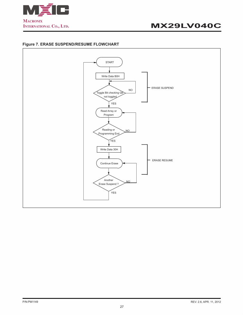
Figure 7. ERASE SUSPEND/RESUME FLOWCHART
START
Write Data B0H
Toggle Bit checking Q6 not toggled
ERASE SUSPEND
YES
NO
Write Data 30H
Continue Erase
Reading or Programming End
Read Array orProgram
AnotherErase Suspend ?
NO
YES
YES
NO
ERASE RESUME

28P/N:PM1149 REV. 2.6, APR. 11, 2012
MX29LV040C
Figure 8. AUTOMATIC PROGRAM TIMING WAVEFORMS
Address
OE#
CE#
A0h
555h PA
PD Status DOUT
VA VA
Tas Tah
Tghwl
Tch
Twp
Tds Tdh
Twhwh1
Last 2 Read Status CycleLast 2 Program Command Cycle
Tcs TwphWE#
Data

29P/N:PM1149 REV. 2.6, APR. 11, 2012
MX29LV040C
Figure 9. CE# CONTROLLED WRITE TIMING WAVEFORM
Address
OE#
CE#
A0h
555h PA
PD Status DOUT
VA VA
Tas Tah
Tghwl
Tcep
Tds Tdh
Twhwh1 or Twhwh2
Tceph
WE#
Data
TwhTws

30P/N:PM1149 REV. 2.6, APR. 11, 2012
MX29LV040C
Figure 10. AUTOMATIC PROGRAMMING ALGORITHM FLOWCHART
START
Write Data AAH Address 555H
Write Data 55H Address 2AAH
Write Program Data/Address
Write Data A0H Address 555H
YES
Read Again Data:Program Data?
YES
Auto Program Completed
Data# Polling Algorithm orToggle Bit Algorithm
next address
Last Byte to beProgramed
No
No

31P/N:PM1149 REV. 2.6, APR. 11, 2012
MX29LV040C
SECTOR PROTECT/CHIP UNPROTECT
Figure 11. SECTOR PROTECT/CHIP UNPROTECT WAVEFORM
150us: Sector Protect15ms: Chip Unprotect1us
Data
SA, A6A1, A0
CE#
WE#
OE#
VA VA VA
Status
VA: valid address
40h60h60h
Verification

32P/N:PM1149 REV. 2.6, APR. 11, 2012
MX29LV040C
Figure 12. SILICON ID READ TIMING WAVEFORM
Taa
Tce
Taa
Toe
Toh Toh
Tdf
DATA OUT
C2H 4FH
Vhv
Vih
VilA9
ADD
CE#
A1
OE#
WE#
A0
DATA OUTDATAQ7~Q0
Vih
Vil
Vih
Vil
Vih
Vil
Vih
Vil
Vih
Vil
Vih
Vil
Vih
Vil

33P/N:PM1149 REV. 2.6, APR. 11, 2012
MX29LV040C
WRITE OPERATION STATUS
Figure 13. DATA# POLLING TIMING WAVEFORMS (DURING AUTOMATIC ALGORITHMS)
Tdf
Tce
Tch
Toe
Toeh
Toh
CE#
OE#
WE#
Q7
Q6~Q0 Status Data Status Data
ComplementComplement True Valid Data
Taa
Trc
Address VAVA
High Z
High ZValid DataTrue

34P/N:PM1149 REV. 2.6, APR. 11, 2012
MX29LV040C
Figure 14. DATA# POLLING ALGORITHM
Read Q7~Q0 at valid address(Note 1)
Read Q7~Q0 at valid address
Start
Q7 = Data# ?
Q5 = 1 ?
Q7 = Data# ?(Note 2)
FAIL Pass
No
No
No
Yes
Yes
Yes
Notes:1.Forprogramming,validaddressmeansprogramaddress.Forerasing,validaddressmeanserasesectorsaddress.2. Q7shouldberecheckedevenQ5="1"becauseQ7maychangesimultaneouslywithQ5.

35P/N:PM1149 REV. 2.6, APR. 11, 2012
MX29LV040C
Figure 15. TOGGLE BIT TIMING WAVEFORMS (DURING AUTOMATIC ALGORITHMS)
Tdf
Tce
Tch
Toe
Toeh
Taa
Trc
Toh
Address
CE#
OE#
WE#
Q6/Q2 Valid Status
(first read)
Valid Status
(second read) (stops toggling)
Valid Data
VA VAVA
VA : Valid Address
VA
Valid Data

36P/N:PM1149 REV. 2.6, APR. 11, 2012
MX29LV040C
Figure 16. TOGGLE BIT ALGORITHM
Notes:1.Readtogglebittwicetodeterminewhetherornotitistoggling.2.RechecktogglebitbecauseitmaystoptogglingasQ5changesto"1".
Read Q7-Q0 Twice
Q5 = 1?
Read Q7~Q0 Twice
PGM/ERS failWrite Reset CMD PGM/ERS Complete
Q6 Toggle ?
Q6 Toggle ?
NO
(Note 1)
YES
NO
NO
YES
YES
Start

37P/N:PM1149 REV. 2.6, APR. 11, 2012
MX29LV040C
RECOMMENDED OPERATING CONDITIONS
At Device Power-Up
ACtimingillustratedinFigureAisrecommendedforthesupplyvoltagesandthecontrolsignalsatdevicepower-up.Ifthetiminginthefigureisignored,thedevicemaynotoperatecorrectly.
Figure A. AC Timing at Device Power-Up
Vcc
ADDRESS
CE#
WE#
OE#
DATA
Tvr
TaaTr or Tf Tr or Tf
TceTf
Vcc(min)
GND
Vih
Vil
Vih
Vil
Vih
Vil
Vih
Vil
Voh High ZVol
ValidOuput
ValidAddress
Tvcs
Tr
ToeTfTr
Symbol Parameter Min. Max. UnitTvr VccRiseTime 20 500000 us/VTr InputSignalRiseTime 20 us/VTf InputSignalFallTime 20 us/V
Note:Nottested100%.

38P/N:PM1149 REV. 2.6, APR. 11, 2012
MX29LV040C
LATCH-UP CHARACTERISTICS
ERASE AND PROGRAMMING PERFORMANCE
PIN CAPACITANCE
Parameter Limits UnitsMin. Typ. Max.ChipEraseTime 4 32 secSectorEraseTime 0.7 8 secErase/ProgramCycles 100,000 CyclesChipProgrammingTime 4.5 13.5 secByteProgrammingTime 9 300 us
Min. Max.InputVoltagedifferencewithGNDonA9,OE#pins -1.0V 12.5VInputVoltagedifferencewithGNDonallI/Opins -1.0V Vcc+1.0VInputcurrentpulse -100mA +100mAAllpinsincludedexceptVcc.Testconditions:Vcc=3.0V,onepinpertesting
Parameter Symbol Parameter Description Test Set Max. UnitCIN2 ControlPinCapacitance VIN=0 12 pFCOUT OutputCapacitance VOUT=0 12 pFCIN InputCapacitance VIN=0 8 pF
DATA RETENTION
Parameter Condition Min. Max. UnitDataretention 55˚C 20 years

39P/N:PM1149 REV. 2.6, APR. 11, 2012
MX29LV040C
ORDERING INFORMATION
PART NO.ACCESS
TIME (ns)
OPERATING CURRENT MAX.
(mA)
STANDBY CURRENT MAX.
(uA)PACKAGE Remark
MX29LV040CTC-55Q 55 30 5 32PinTSOP(8x20mm)
MX29LV040CTC-70G 70 30 5 32PinTSOP(8x20mm)
MX29LV040CTC-90G 90 30 5 32PinTSOP(8x20mm)
MX29LV040CQC-55Q 55 30 5 32PinPLCC MX29LV040CQC-70G 70 30 5 32PinPLCC MX29LV040CQC-90G 90 30 5 32PinPLCC
MX29LV040CTI-55Q 55 30 5 32PinTSOP(8x20mm)
MX29LV040CTI-70G 70 30 5 32PinTSOP(8x20mm)
MX29LV040CTI-90G 90 30 5 32PinTSOP(8x20mm)
MX29LV040CQI-55Q 55 30 5 32PinPLCC MX29LV040CQI-70G 70 30 5 32PinPLCC MX29LV040CQI-90G 90 30 5 32PinPLCC
MX29LV040CT2I-70G 70 30 5 32PinTSOP(8x14mm)
MX29LV040CT2I-90G 90 30 5 32PinTSOP(8x14mm)

40P/N:PM1149 REV. 2.6, APR. 11, 2012
MX29LV040C
PART NAME DESCRIPTION
MX 29 LV 70C T C GOPTION:G: RoHS compliant packageQ: Restricted VCC (3.0V~3.6V) with RoHS compliant package
SPEED:55: 55ns70: 70ns90: 90ns
TEMPERATURE RANGE:C: Commercial (0°C to 70°C)I: Industrial (-40°C to 85°C)
PACKAGE:Q: PLCCT: TSOP (8mm x 20mm)T2: TSOP (8mm x 14mm)
REVISION:C
DENSITY & MODE:040: 4M, x8 Equal Sector
TYPE:L, LV: 3V
DEVICE:29:Flash
040

41P/N:PM1149 REV. 2.6, APR. 11, 2012
MX29LV040C
PACKAGE INFORMATION

42P/N:PM1149 REV. 2.6, APR. 11, 2012
MX29LV040C

43P/N:PM1149 REV. 2.6, APR. 11, 2012
MX29LV040C

44P/N:PM1149 REV. 2.6, APR. 11, 2012
MX29LV040C
REVISION HISTORY
Revision No. Description Page Date1.0 1.Removed"Preliminary" P1 JUN/30/2005 2.Added"RecommendedOperatingConditions" P431.1 1.Modified"Lowpowerconsumption--activecurrent"from20mA(Max.)P1 AUG/30/2005 to30mA(Max.) 2.AddeddescriptionaboutPb-freedevicesareRoHSCompliant P11.2 1.ModifiedEraseResumefromdelay10mstodelay400us P12,32 JAN/17/20061.3 1.Modifiedtable15.CFImode P45,46 APR/24/2006 2.AddedVLKOdescription P15,181.4 1.ModifiedCFImode P45,46 JUL/11/20061.5 1.Datasheetformatchanged All AUG/15/20061.6 1.Datamodification All AUG/16/20061.7 1.Datamodification All AUG/17/20061.8 1.Addedstatement P44 NOV/06/20061.9 1.Revisedstatement P14 DEC/28/20072.0 1.Addednote1intotable3.CommandDefinitions P9 JAN/17/20082.1 1.ModifiedFigure9.CE#ControlledWriteTimingWaveform P29 FEB/21/20082.2 1.RevisedTwc,Tcwc,TdsACtimingspec P20 JUL/31/20082.3 1.Added32-TSOP(8mmx14mm)packageinformation P1,2,39 MAR/25/2009 P40,432.4 1.Addeddataretentiontable P38 AUG/21/2009 2.Modifiedthesectorerasetimemaxfrom15sto8s P38 3.DeletedLeadEPN P39,402.5 1.ModifieddescriptionforRoHScompliance P1,40 DEC/15/2011 2.Addednote P372.6 1.ModifiedPartNameDescription P40 APR/11/2012 2.ModifiedFigure9.CE#ControlledWriteTimingWaveform P29

MX29LV040C
45
MACRONIX INTERNATIONAL CO., LTD. reserves the right to change product and specifications without notice.
Except forcustomizedproductswhichhasbeenexpressly identified in theapplicableagreement,Macronix'sproducts aredesigned, developed, and/ormanufactured for ordinary business, industrial, personal, and/orhouseholdapplicationsonly,andnotforuseinanyapplicationswhichmay,directlyorindirectly,causedeath,personalinjury,orseverepropertydamages.IntheeventMacronixproductsareusedincontradictedtotheirtargetusageabove,thebuyershalltakeanyandallactionstoensuresaidMacronix'sproductqualifiedforitsactualuseinaccordancewiththeapplicablelawsandregulations;andMacronixaswellasit’ssuppliersand/ordistributorsshallbereleasedfromanyandallliabilityarisentherefrom.
Copyright©Macronix InternationalCo., Ltd. 2006~2012.All rights reserved, including the trademarksandtradename thereof, suchasMacronix,MXIC,MXICLogo,MXLogo, IntegratedSolutionsProvider,NBit,Nbit,NBiit,MacronixNBit,eLiteFlash,XtraROM,Phines,KHLogo,BE-SONOS,KSMC,Kingtech,MXSMIO,Macronix vEE,MacronixMAP,RichAudio,RichBook,RichTV, andFitCAM.Thenamesandbrandsofother companiesare for identificationpurposesonly andmaybe claimedas theproperty of the respectivecompanies.
Forthecontactandorderinformation,pleasevisitMacronix’sWebsiteat:http://www.macronix.com