Embed Size (px)
Citation preview

30 MHz to 520 MHz Digitally Tunable Band-Pass Filter
Preliminary Technical Data ADMV8052
Rev. PrK Document Feedback Information furnished by Analog Devices is believed to be accurate and reliable. However, no responsibility is assumed by Analog Devices for its use, nor for any infringements of patents or other rights of third parties that may result from its use. Specifications subject to change without notice. No license is granted by implication or otherwise under any patent or patent rights of Analog Devices. Trademarks and registered trademarks are the property of their respective owners.
One Technology Way, P.O. Box 9106, Norwood, MA 02062-9106, U.S.A. Tel: 781.329.4700 ©2021 Analog Devices, Inc. All rights reserved. Technical Support www.analog.com
FEATURES Digitally tunable, multioctave, band-pass tuning 3dB Bandwidth (BW): 7 to 11% Low Insertion Loss: 4dB @ 9% BW Excellent rejection: 20 dB @ 2 x BW Great Linearity Single chip replacement for discrete solutions Compact 22 × 22 x 5.73 mm LGA package
APPLICATIONS Land mobile radio Test and measurement equipment Military radar and electronic warfare/electronic
countermeasures Satellite communications Industrial and medical equipment
GENERAL DESCRIPTION The ADMV8052 is a radio frequency filter, that features a digitally selectable frequency of operation. The device has three band-pass filters, that span across three specified bands from 30 to 520 MHz.
The center frequency (fC) of operation can be adjusted using an 8-bit value (256 states) that incorporates a patent pending interpolation technique. The typical 3 dB bandwidth (BW) is 9% and adjustability is ± 2%. Insertion loss is typically 4 dB, and rejection at 2 x BW is 20 dB, which is ideally suited for minimizing system harmonics. Additionally, the flexible architecture incorporates a bypass mode with a low insertion loss of 1 dB.
This tunable filter can be used as a smaller alternative to large switched filter banks and cavity tuned filters, and this device provides a dynamically adjustable solution in advanced communications applications.
FUNCTIONAL BLOCK DIAGRAM
Figure 1.
SDO 9
5
1
21
25
17
29
1310 11 12 14 15 16
8
7
6
4
3
2
32 31 30 28 27 26
18
19
20
22
23
24
CS
SCLK
RST
GND
RF1
GND
GND
GND
SDI
SFL
GN
D
GN
D
GN
D
GN
D
VDD
(+3.
3V)
GND
BYP
VSS(-2.5V)
GND
RF2
GND
GND
GND
GND
GN
D
GN
D
GN
D
GN
D
GN
D
GN
D
GN
D
SPI
BYPASS
LUT
INTERPOLATION
CHIPRESET
MODESELECT
LDO+2.5V
1
2
3

ADMV8052 Preliminary Technical Data
Rev. PrK | Page 2 of 56
TABLE OF CONTENTS Features .............................................................................................. 1 Applications ....................................................................................... 1
General Description ..................................................................... 1 Functional Block Diagram .............................................................. 1 Revision History .......................... Error! Bookmark not defined. Specifications ..................................................................................... 3
Timing Specifications .................................................................. 4 Absolute Maximum Ratings ............................................................ 5
Electrostatic Discharge (ESD) Ratings ...................................... 5 ESD Caution .................................................................................. 5
Pin Descriptions ............................................................................... 6 Typical Performance Characteristics ............................................. 7
Band 1 ............................................................................................ 7 Theory of Operation ........................................................................ 9
Chip Architecture ......................................................................... 9 RF Connections ............................................................................ 9 SPI Configuration ......................................................................... 9 Mode Selection ........................................................................... 10 SPI Write Mode ........................................................................... 10
Switch Positions .......................................................................... 10 Switch Set..................................................................................... 10 Write Group Priority .................................................................. 10 Interpolation Functions ............................................................. 11 Interpolation Equations ............................................................. 11 Interpolation Tables ................................................................... 12 Interpolation Plots...................................................................... 12 Interpolation Coefficient Calibration ...................................... 13 Filter Code Read Back ............................................................... 13 Tracking ....................................................................................... 13 SPI Fast Latch Mode .................................................................. 13 Chip Reset ................................................................................... 14
Applications Information .............................................................. 15 PCB Design Guidelines ............................................................. 15
Flow Charts ..................................................................................... 16 Register Summary .......................................................................... 18 Register Details ............................................................................... 30 Outline Dimensions ....................................................................... 56

Preliminary Technical Data ADMV8052
Rev. PrK | Page 3 of 56
SPECIFICATIONS TA = 25°C, unless otherwise noted.
Table 1. Parameter Min Typ Max Unit Test Conditions/Comments
CENTER FREQUENCY RANGE (fC) Band 1 30 89.99 MHz Band 2 90 224.99 MHz Band 3 225 520 MHz Bypass 5 3000 MHz
BANDWIDTH (3 dB) 7 9 11 %
RESOLUTION Varies with respect to center frequency, please refer to section TBD for more information.
Band 1 235 kHz Band 2 530 kHz Band 3 1.15 MHz
REJECTION 2 x BW 20 dB Reentry 3 GHz ≤30 dB
INSERTION LOSS Bypass Mode 1 dB BPF 4 dB
RETURN LOSS 20 dB
DYNAMIC PERFORMANCE Input Compression (P0.1dB) TBD dBm Input Third-Order Intercept (IP3) TBD dBm Group Delay Flatness TBD ns Amplitude Settling Time TBD ns To within ≤0.5 dB of static insertion loss Phase Settling Time TBD µsec To within ≤5° of static phase Drift Rate
Amplitude TBD dB/°C At TBD MHz Frequency TBD ppm/°C
RESIDUAL PHASE NOISE At 1 MHz to 10 MHz Offset TBD dBc/Hz
SUPPLY VOLTAGE VSS -2.6 -2.5 -2.4 V VDD +3.2 +3.3 +3.4 V
SUPPLY CURRENT (STATIC) VSS TBD µA VDD TBD µA
SUPPLY CURRENT (DYNAMIC) VDD TBD mA Where fSCLK is the SCLK toggle frequency in MHz,
for example, continuous SPI writing at 10 MHz yield TBD mA of dynamic supply current
LOGIC (Error! Bookmark not defined.RST, CS, SCLK, SDI, SDO, SFL)
Logic Low –0.3 0 +0.8 V Logic High +1.2 +3.3 +3.6 V

ADMV8052 Preliminary Technical Data
Rev. PrK | Page 4 of 56
TIMING SPECIFICATIONS
Table 2. Parameter Min Typ Max Unit Test Conditions / Comments t1 10 ns RST low time to perform reset
10 ns SCLK cycle time (write) t2 20 ns SCLK cycle time (read) t3 2.5 ns SCLK high time t4 2.5 ns SCLK low time t5 5 ns CS falling edge to SCLK rising edge setup time
t6 2 ns SCLK rising edge to CS hold time
t7 5 ns Minimum CS high time for latching in data (for multiple SPI transactions)
t8 5 ns CS rising edge to next SCLK rising edge ignore
t9 5 ns SDI data setup time t10 2 ns SDI data hold time t11 10 ns SFL falling edge (exiting SFL mode) to CS falling edge time (start SPI transaction)
t12 10 ns CS rising edge (end SPI transaction) to SFL rising edge time (entering SFL mode)
t13 10 ns SFL rising edge to CS falling edge time
t14 10 ns CS cycle time (SFL mode)
t15 2.5 ns CS high time (SFL mode)
t16 2.5 ns CS low time (SFL mode)
t17 6 ns SCLK falling edge to SDO valid (load capacitance (CL) = 10 pF) t18 5 ns SDO rise and fall time (CL = 10 pF) t19 4 ns CS rising edge to SDO tristate (CL = 10 pF)
Timing Diagram
Figure 2. Timing Diagram
1 2
t2
t4
SCLK
CS
SDI
SFL
RST
SDO
t3
t5
t7
t6
t8
R/W
t9
t10
t11t12 t13
t15
t16
t1
3
A14 to A0
17 18 19 20 21 22 23 24
D7 D6 D5 D4 D3 D2 D1 D0
t14
≈
D7 D6 D5 D4 D3 D2 D1 D0Don’t Care
t17
t18
t19
Note: for read operation the data bits on SDI are don’t cares.
4 5

Preliminary Technical Data ADMV8052
Rev. PrK | Page 5 of 56
ABSOLUTE MAXIMUM RATINGS Table 3.
Parameter Rating SUPPLY
VDD −0.3 V to +3.6 V VSS −3.6 V to +0.3 V
Digital Control Inputs Voltage −0.3 V to VDD + 0.3 V Current 2 mA
RF Input Power P0.1dB1 Temperature
Operating Range −55°C to +105°C Storage Temperature Range −65°C to +150°C Junction to Maintain 1 Million
Hours Mean Time to Failure (MTTF)
135°C
Nominal Junction (TPADDDLE = 85°C) 90°C Moisture Sensitivity Level (MSL) Rating MSL3
1 Note that P0.1dB varies with filter settings. Please see Figure TBD.
Stresses at or above those listed under Absolute Maximum Ratings may cause permanent damage to the product. This is a stress rating only; functional operation of the product at these or any other conditions above those indicated in the operational section of this specification is not implied. Operation beyond the maximum operating conditions for extended periods may affect product reliability.
ELECTROSTATIC DISCHARGE (ESD) RATINGS The following ESD information is provided for handling of ESD-sensitive devices in an ESD protected area only.
Human body model (HBM) per ANSI/ESDA/JEDEC JS-001.
Field induced charged device model (FICDM) per ANSI/ESDA/ JEDEC JS-002.
ESD Ratings for ADMV8052
Table 4. ADMV8052, 32-Terminal LGA ESD Model Withstand Threshold (V) Class HBM 2000 2 FICDM 250 C3
ESD CAUTION

ADMV8052 Preliminary Technical Data
Rev. PrK | Page 6 of 56
PIN DESCRIPTIONSTable 5. Pin Function Descriptions
Pin No. Mnemonic Description 1 to 4, 12 to 15, 17, 20, 22 to 32
GND Ground. Connect the GND pins to the RF and dc ground.
5 RF1 RF Pin 1. This pin is dc-coupled and matched to 50 Ω. Do not apply an external voltage to this pin. 6 RST Chip Reset. 3.3 V logic. Active low. The RST pin is internally pulled high with a 260 kΩ resistor.
7 SCLK Serial Peripheral Interface (SPI) Clock. 3.3 V logic. The SCLK pin is internally pulled low with a 260 kΩ resistor.
8 CS SPI Chip Select. 3.3 V logic. Active low. The CS pin is internally pulled low with a 260 kΩ resistor.
9 SDO SPI Data Output. 3.3 V logic. The SDO pin is internally pulled low with a 260 kΩ resistor. 10 SDI SPI Data Input. 3.3 V logic. The SDI pin is internally pulled low with a 260 kΩ resistor. 11 SFL SPI Fast Latch Enable. 3.3 V logic. Set SFL high to enable fast latching of filter states on each rising edge
of CS. While SFL is in this mode, the SCLK, SDO, and SDI pins are not active. The SFL pin is internally pulled low with a 260 kΩ resistor.
16 VDD +3.3 V Power Supply Pin. Place 0.1 µF and 100 pF decoupling capacitors close to VDD. 18 BYP +2.5 V LDO Bypass Pin. Place 47 µF, 0.1 µF, and 100 pF decoupling capacitors close to BYP. 19 VSS –2.5 V Power Supply Pin. Place 0.1 µF and 100 pF decoupling capacitors close to VSS. 21 RF2 RF Pin 2. This pin is dc-coupled and matched to 50 Ω. Do not apply an external voltage to this pin. E1 to E16 EPAD Exposed Pad. The exposed pad must be connected to the RF and dc ground.

Preliminary Technical Data ADMV8052
Rev. PrK | Page 7 of 56
TYPICAL PERFORMANCE CHARACTERISTICS BAND 1
Figure 3. Insertion Loss vs RF Frequency for 9% Bandwidth
Figure 4. Insertion Loss and Return Loss vs RF Frequency for 9%
Bandwidth at 30 MHz
Figure 5. Insertion Loss and Group Delay vs RF Frequency for 9%
Bandwidth at 30 MHz
Figure 6. Insertion Loss vs RF Frequency for 9% Bandwidth and Various
Temperatures
Figure 7. Insertion Loss and Return Loss vs RF Frequency for 9%
Bandwidth at 90 MHz
Figure 8. Insertion Loss and Group Delay vs RF Frequency for 9%
Bandwidth at 90 MHz
TBD
TBD
TBD
TBD
TBD
TBD

ADMV8052 Preliminary Technical Data
Rev. PrK | Page 8 of 56
Figure 9. Insertion Loss vs RF Frequency at 30 MHz and Various
Bandwidths
Figure 10. Input IP3 vs. RF Frequency for Condition TBD and Various
Temperatures
Figure 11. Residual Phase Noise vs Offset Frequency
Figure 12. Insertion Loss vs RF Frequency at 90 MHz and Various
Bandwidths
Figure 13. Input P0.1dB vs. RF Frequency for Condition TBD and Various
Temperatures
Figure 14. Center Frequency and Step Size vs FC_LOAD
TBD
TBD
TBD
TBD
TBD
TBD

Preliminary Technical Data ADMV8052
Rev. PrK | Page 9 of 56
THEORY OF OPERATION CHIP ARCHITECTURE The ADMV8052 contains three band-pass filters and an optional bypass configuration selectable by two SP4T switches. The device provides full coverage over the frequency band without any dead zones. Figure 1 is a conceptual block diagram of the ADMV8052.
Each band within the ADMV8052 contains several switched capacitors that allow the RF performance to be varied. A simplified diagram of the filter architecture is shown below in Figure 15.
Figure 15. Simplified Filter Architecture Diagram
The two CFC capacitors are configured by the FC load value, that will manipulate the center frequency of the filter. Likewise, the CBW capacitor is configured by the BW load value, that will adjust bandwidth response of the filter. Additionally, the two CMATCH capacitors are set by the MATCH load value, that will allow for adjustments to impedance matching of the filter.
The FC, BW, and MATCH load values each have 256 states (8 bits). In theory there are over 16 Million possible states for FC, BW, and MATCH load values for each band within the ADMV8052. To simplify selection of these values, Analog Devices has developed three patent pending interpolation functions to ease implementation.
RF CONNECTIONS The RF1 and RF2 pins of the ADMV8052 are DC coupled to on chip RF switches. If a dc voltage is present on the RF1 and RF2 pins from other components within the system, it is recommended to place dc blocking capacitors in series with these pins. The dc blocking capacitors must be selected based on the operating frequency of the filter. Generally, a value greater than 10 nF is sufficient to minimize insertion loss at the lower frequencies of operation. At higher frequencies of operation, it may be necessary to consider the parasitic elements of the selected capacitor. Figure 16 shows a general model of a capacitor with the parasitic elements. The parasitic series inductance (LESL) is typically of most concern given that its impedance can become dominant. The other parasitic elements, including the leakage resistance (RL), the dielectric absorption resistance (RDA), the dielectric absorption capacitance (CDA), and electrical series resistance (RESR) are less critical elements for consideration but are shown here for completeness.
Figure 16. Model of a Capacitor
SPI CONFIGURATION The SPI of the ADMV8052 allows configuration of the device for specific functions or operations via the 5-pin SPI port. This interface provides users with added flexibility and customization. The SPI consists of five control lines: SFL, SCLK, SDI, SDO, and CS. For normal SPI operations, keep the SFL pin low.
The SPI protocol consists of an R/W bit followed by 15 register address bits and 8 data bits. The address field and data field are organized MSB first and end with the LSB.
Set the MSB to 0 for a write operation and set the MSB to 1 for a read operation. The write cycle must be sampled on the rising edge of SCLK. The 24 bits of the serial write address and data are shifted in on the SDI control line, MSB to LSB. The ADMV8052 input logic level for the write cycle supports a 3.3 V interface.
For a read cycle, the R/W bit and the 15 register address bits shift in on the rising edge of SCLK on the SDI control line. Then, 8 bits of serial read data shift out on the SDO control line, MSB first, on the falling edge of SCLK. The output logic level for a read cycle is 3.3 V. The output drivers of the SDO are enabled after the last rising edge of SCLK of the instruction cycle and remain active until the end of the read cycle. In a read operation, when CS is deasserted, SDO returns to high impedance until the next read transaction. CS is active low and must be deasserted at the end of the write or read sequence.
An active low input on CS starts and gates a communication cycle. The CS pin allows more than one device to be used on the same serial communications lines. The SDO pin goes to a high impedance state when the CS input is high. During the communication cycle, the chip select must stay low. The SPI communications protocol follows the Analog Devices SPI standard. For more information, see the ADI-SPI Serial Control Interface Standard (Rev 1.0).
LCFC<7:0>
CBW<7:0>
CMATCH<7:0>
L CFC<7:0>
CMATCH<7:0>
LESLC
RL
RESR
RDA CDA
2560
3-04
9

ADMV8052 Preliminary Technical Data
Rev. PrK | Page 10 of 56
MODE SELECTION The ADMV8052 has two modes of operation: SPI write and SPI fast latch. SPI write mode is the normal operating mode, whereas SPI fast latch mode is used to sequence through the on-chip lookup table (LUT) using the internal state machine. To select SPI write mode, set the SFL pin low. For operation in SPI fast latch mode, program the on-chip lookup table and fast latch parameters with the SFL pin low, and then bring the SFL pin high to enter this mode. Figure 17 shows a simplified representation of the SPI with the register map and internal state machine. Refer to the programming flow chart in Figure 22 for the typical steps to operate in each mode.
Figure 17. Simplified SPI Diagram
SPI WRITE MODE The SPI Write mode has four write groupings, WR0 through WR3 in registers 0x020 through 0x02F. The groupings can be thought of as a small lookup table for the SPI Write mode. Each group consists of the following:
• Switch Position • Switch Set • FC Load Value • BW Load Value • MATCH Load Value
See the Register Details section for an example of the write grouping of WR0 (Register 0x020 and Register 0x023).
SWITCH POSITIONS The ADMV8052 contains three band-pass filters and an optional bypass, that is selectable by using the on-chip RF switches. The Switch Position bits will dictate which filter the FC, BW, and MATCH load values will be assigned. For example in write group WR0 (register 0x020), when SW_WR0 is set for band 2, then FC_LOAD_WR0 (register 0x021), BW_LOAD_WR0 (register 0x022), and MATCH_LOAD_WR0 (register 0x023) will be applied to band-pass filter 2.
SWITCH SET The Switch Set bit is used to determine if the Switch Position shall be moved to that setting. This can useful for configuring a filter to a known state and leaving the switch position unchanged (switch set bit low). For most applications the switch set bit would be high.
WRITE GROUP PRIORITY In SPI Write mode, because there are four write groupings, it is possible that multiple switch set bits are high. The behavior of the switches will depend upon the type of SPI transaction, either streaming or single instruction.
In general, there are two types of SPI streaming transactions, Endian register ascending order and descending order. The ADMV8052 supports the ascending order only. To enable SPI streaming with Endian register ascending order, program Register 0x000 to 0x3C.
For SPI streaming transactions (recommended) the priority order for the switch set bits will be WR0 to WR3. The SPI streaming transaction for Register 0x020 to Register 0x02F then points to Address 0x020 and streams out 16 bytes of data. The SPI streaming transaction is 144 bits in total (R/W bit + 15 address bits + 128 data bits).
An example of the priority order for an SPI streaming transaction follows: if the switch set bits are high for both WR1 and WR2, the resulting switch positions are the positions programmed in WR1.
For SPI single instruction transactions, the most recently programmed switch set will take effect to move the switch positions.
To use SPI single instruction transactions, the switch register must be written first followed by the filter setting registers. For example, to use write grouping WR0, Register 0x020 would be written first using a 24 bit transaction (R/W bit + 15 bits address + 8 bits data), followed by a writing Register 0x021, Register 0x022, and Register 0x023, each using a 24 bit transaction.
SCLKREGISTER MAP
PARAMETERS ANDLOOKUP TABLE
INTERNAL STATEMACHINE
START LOCATION...
STOP LOCATIONWR
SDOSDI
CS
SFL
FILTERS
2560
3-05
0

Preliminary Technical Data ADMV8052
Rev. PrK | Page 11 of 56
INTERPOLATION FUNCTIONS The ADMV8052 has three interpolation functions that allow the user to specify only the center frequency of the filter using the FC load value, and then the appropriate capacitor codes will be determined automatically. To enable these functions, the INTERPOLATE bit (register 0x050) must be set high. Shown below in Figure 18 is a simplified diagram of the interpolation functions.
Figure 18. Interpolation Diagram
When the interpolation functions are enabled, the FC load range will be 0 to 255, where 0 corresponds to the lowest frequency within a band, and 255 corresponds to the highest frequency within a band. For example, when band 1 is selected, a value of 0 would correspond to approximately 30MHz, and a value of 255 would correspond to approximately 90MHz. The FC load value will be used to determine the appropriate capacitor codes based upon the on-chip interpolation coefficients.
By default, the recommended interpolation coefficients are set for 9% bandwidth. The interpolation coefficients can be adjusted to achieve bandwidths between 7 and 11% with reasonable insertion loss. Narrower bandwidth down to approximately 5% can also be achieved at the expense of insertion loss.
INTERPOLATION EQUATIONS Below are equations describing the input to the interpolation functions: 𝐹𝐹𝐶𝐶𝐶𝐶𝐶𝐶𝐶𝐶 = min(𝑀𝑀𝑀𝑀𝑀𝑀𝑀𝑀𝑀𝑀𝑀𝑀𝑀𝑀 𝐶𝐶𝐶𝐶𝑀𝑀𝐶𝐶𝐶𝐶𝐶𝐶 𝐹𝐹𝐶𝐶𝐶𝐶𝐹𝐹𝑀𝑀𝐶𝐶𝑀𝑀𝐹𝐹𝐹𝐹 𝑓𝑓𝑓𝑓𝐶𝐶 𝑆𝑆𝐶𝐶𝑆𝑆𝐶𝐶𝐹𝐹𝐶𝐶𝐶𝐶𝑆𝑆 𝐵𝐵𝐵𝐵𝑀𝑀𝑆𝑆)
𝐹𝐹𝐶𝐶𝐶𝐶𝐶𝐶𝐶𝐶 = max(𝑀𝑀𝐵𝐵𝑀𝑀𝑀𝑀𝑀𝑀𝑀𝑀𝑀𝑀 𝐶𝐶𝐶𝐶𝑀𝑀𝐶𝐶𝐶𝐶𝐶𝐶 𝐹𝐹𝐶𝐶𝐶𝐶𝐹𝐹𝑀𝑀𝐶𝐶𝑀𝑀𝐹𝐹𝐹𝐹 𝑓𝑓𝑓𝑓𝐶𝐶 𝑆𝑆𝐶𝐶𝑆𝑆𝐶𝐶𝐹𝐹𝐶𝐶𝐶𝐶𝑆𝑆 𝐵𝐵𝐵𝐵𝑀𝑀𝑆𝑆)
𝐹𝐹𝐶𝐶𝐶𝐶𝐶𝐶𝐶𝐶𝐶𝐶 ≈𝐹𝐹𝐶𝐶𝐶𝐶𝐶𝐶𝐶𝐶 − 𝐹𝐹𝐶𝐶𝐶𝐶𝐶𝐶𝐶𝐶
255
𝑋𝑋 = 𝐹𝐹𝐶𝐶_𝐿𝐿𝐿𝐿𝐿𝐿𝐿𝐿 < 7: 0 >
The anticipated center frequency of the filter is then computed as:
𝐹𝐹𝐶𝐶 ≈ 𝐹𝐹𝐶𝐶𝐶𝐶𝐶𝐶𝐶𝐶 + 𝐹𝐹𝐶𝐶𝐶𝐶𝐶𝐶𝐶𝐶𝐶𝐶 ∙ 𝑋𝑋
The equations for the interpolation function Y = f(X) that determines the center frequency capacitor codes are as follows:
Condition Logic Shift Form
𝑀𝑀𝑓𝑓(0 ≤ 𝑋𝑋 < 16) 𝑌𝑌 = 𝑌𝑌1 + [((16− 𝑋𝑋)(𝑌𝑌0 − 𝑌𝑌1)) ≫ 4]
𝑀𝑀𝑓𝑓(16 ≤ 𝑋𝑋 < 32) 𝑌𝑌 = 𝑌𝑌2 + [((32− 𝑋𝑋)(𝑌𝑌1 − 𝑌𝑌2)) ≫ 4]
𝑀𝑀𝑓𝑓(32 ≤ 𝑋𝑋 < 64) 𝑌𝑌 = 𝑌𝑌3 + [((64− 𝑋𝑋)(𝑌𝑌2 − 𝑌𝑌3)) ≫ 5]
𝑀𝑀𝑓𝑓(64 ≤ 𝑋𝑋 < 96) 𝑌𝑌 = 𝑌𝑌4 + [((96− 𝑋𝑋)(𝑌𝑌3 − 𝑌𝑌4)) ≫ 5]
𝑀𝑀𝑓𝑓(96 ≤ 𝑋𝑋 < 128) 𝑌𝑌 = 𝑌𝑌5 + [((128− 𝑋𝑋)(𝑌𝑌4 − 𝑌𝑌5)) ≫ 5]
𝑀𝑀𝑓𝑓(128 ≤ 𝑋𝑋 < 160) 𝑌𝑌 = 𝑌𝑌6 + [((160− 𝑋𝑋)(𝑌𝑌5 − 𝑌𝑌6)) ≫ 5]
𝑀𝑀𝑓𝑓(160 ≤ 𝑋𝑋 < 192) 𝑌𝑌 = 𝑌𝑌7 + [((192− 𝑋𝑋)(𝑌𝑌6 − 𝑌𝑌7)) ≫ 5]
𝑀𝑀𝑓𝑓(192 ≤ 𝑋𝑋 < 224) 𝑌𝑌 = 𝑌𝑌8 + [((224− 𝑋𝑋)(𝑌𝑌7 − 𝑌𝑌8)) ≫ 5]
𝑀𝑀𝑓𝑓(224 ≤ 𝑋𝑋 < 255) 𝑌𝑌 = 𝑌𝑌9 + [((256− 𝑋𝑋)(𝑌𝑌8 − 𝑌𝑌9)) ≫ 5]
𝐶𝐶𝑆𝑆𝑒𝑒𝐶𝐶 𝑌𝑌 = 𝑌𝑌9
where Y0 to Y9 are the FC coefficients for the selected band
The equations for the interpolation function V = f(Y) that determines the bandwidth capacitor codes are as follows:
Condition Logic Shift Form
𝑀𝑀𝑓𝑓(0 ≤ 𝑌𝑌 < 32) 𝑉𝑉 = 𝑉𝑉0 + [(𝑌𝑌 ∙ (𝑉𝑉1 − 𝑉𝑉0)) ≫ 5]
𝑀𝑀𝑓𝑓(32 ≤ 𝑌𝑌 < 255) 𝑉𝑉 = 𝑉𝑉1 + (𝑌𝑌 − 32)(𝑉𝑉2 − 𝑉𝑉1) ∙ 295 ≫ 16
𝐶𝐶𝑆𝑆𝑒𝑒𝐶𝐶 𝑉𝑉 = 𝑉𝑉2
where V0 to V2 are the BW coefficients for the selected band
The equations for the interpolation function T = f(Y) that determines the bandwidth capacitor codes are as follows:
Condition Logic Shift Form
𝑀𝑀𝑓𝑓(0 ≤ 𝑌𝑌 < 32) 𝑇𝑇 = 𝑇𝑇0 + [(𝑌𝑌 ∙ (𝑇𝑇1 − 𝑇𝑇0)) ≫ 5]
𝑀𝑀𝑓𝑓(32 ≤ 𝑌𝑌 < 255) 𝑇𝑇 = 𝑇𝑇1 + (𝑌𝑌 − 32)(𝑇𝑇2 − 𝑇𝑇1) ∙ 295 ≫ 16
𝐶𝐶𝑆𝑆𝑒𝑒𝐶𝐶 𝑇𝑇 = 𝑇𝑇2
where T0 to T2 are the MATCH coefficients for the selected band
BWz_INT<7:0>
Y = f(X)
X Y
Y0Y1Y9
Register Map
V = f(Y)
Y V
V0V1V2
T = f(Y)
Y T
T0T1T2
FC_LOAD<7:0>
BW_LOAD<7:0>
MATCH_LOAD<7:0>
Selected Band
CFC<7:0>
FCz_INT<7:0>
INTERPOLATE = 1
CBW<7:0>
CMATCH<7:0>
BANDz_INTERP_FC_Y9
BANDz_INTERP_FC_Y1BANDz_INTERP_FC_Y0
BANDz_INTERP_BW_V2BANDz_INTERP_BW_V1BANDz_INTERP_BW_V0
BANDz_INTERP_MATCH_T2BANDz_INTERP_MATCH_T1BANDz_INTERP_MATCH_T0
MATCHz_INT<7:0>
where z is the selected band number

ADMV8052 Preliminary Technical Data
Rev. PrK | Page 12 of 56
INTERPOLATION TABLES Solving the interpolation equations for the lower bounds of each condition in the interpolation function Y = f(X) yields the following table:
X FC Y = f(X)
0 𝐹𝐹𝐶𝐶 ≈ 𝐹𝐹𝐶𝐶𝐶𝐶𝐶𝐶𝐶𝐶 𝑌𝑌0
16 𝐹𝐹𝐶𝐶 ≈ 𝐹𝐹𝐶𝐶𝐶𝐶𝐶𝐶𝐶𝐶 + 𝐹𝐹𝐶𝐶𝐶𝐶𝐶𝐶𝐶𝐶𝐶𝐶 ∙ 16 𝑌𝑌1
32 𝐹𝐹𝐶𝐶 ≈ 𝐹𝐹𝐶𝐶𝐶𝐶𝐶𝐶𝐶𝐶 + 𝐹𝐹𝐶𝐶𝐶𝐶𝐶𝐶𝐶𝐶𝐶𝐶 ∙ 32 𝑌𝑌2
64 𝐹𝐹𝐶𝐶 ≈ 𝐹𝐹𝐶𝐶𝐶𝐶𝐶𝐶𝐶𝐶 + 𝐹𝐹𝐶𝐶𝐶𝐶𝐶𝐶𝐶𝐶𝐶𝐶 ∙ 64 𝑌𝑌3
96 𝐹𝐹𝐶𝐶 ≈ 𝐹𝐹𝐶𝐶𝐶𝐶𝐶𝐶𝐶𝐶 + 𝐹𝐹𝐶𝐶𝐶𝐶𝐶𝐶𝐶𝐶𝐶𝐶 ∙ 96 𝑌𝑌4
128 𝐹𝐹𝐶𝐶 ≈ 𝐹𝐹𝐶𝐶𝐶𝐶𝐶𝐶𝐶𝐶 + 𝐹𝐹𝐶𝐶𝐶𝐶𝐶𝐶𝐶𝐶𝐶𝐶 ∙ 128 𝑌𝑌5
160 𝐹𝐹𝐶𝐶 ≈ 𝐹𝐹𝐶𝐶𝐶𝐶𝐶𝐶𝐶𝐶 + 𝐹𝐹𝐶𝐶𝐶𝐶𝐶𝐶𝐶𝐶𝐶𝐶 ∙ 160 𝑌𝑌6
192 𝐹𝐹𝐶𝐶 ≈ 𝐹𝐹𝐶𝐶𝐶𝐶𝐶𝐶𝐶𝐶 + 𝐹𝐹𝐶𝐶𝐶𝐶𝐶𝐶𝐶𝐶𝐶𝐶 ∙ 192 𝑌𝑌7
224 𝐹𝐹𝐶𝐶 ≈ 𝐹𝐹𝐶𝐶𝐶𝐶𝐶𝐶𝐶𝐶 + 𝐹𝐹𝐶𝐶𝐶𝐶𝐶𝐶𝐶𝐶𝐶𝐶 ∙ 224 𝑌𝑌8
255 𝐹𝐹𝐶𝐶 ≈ 𝐹𝐹𝐶𝐶𝐶𝐶𝐶𝐶𝐶𝐶 𝑌𝑌9
Table 6.
Similarly, solving the equations for the lower bounds of each condition in the interpolation functions V = f(Y) and T = f(Y) yields:
Y V = f(Y) T = f(Y)
0 𝑉𝑉0 𝑇𝑇0
32 𝑉𝑉1 𝑇𝑇1
255 𝑉𝑉2 𝑇𝑇2
Table 7.
INTERPOLATION PLOTS To garner a visual representation of the interpolation functions, the interpolation coefficients vs their input (from the interpolation tables) can be plotted on a scatter plot. Shown below in Figure 19, Figure 20, and Figure 21 are the interpolation functions Y, V, and T using the interpolation coefficients for band 1.
Figure 19. Interpolation Function Y = f(X)
Figure 20. Interpolation Function V = f(Y)
Figure 21. Interpolation Function T = f(Y)
Y0 = 225
Y1 = 175
Y2 = 140
Y3 = 94
Y4 = 67Y5 = 49
Y6 = 37Y7 = 29
Y8 = 23Y9 = 18
0
32
64
96
128
160
192
224
256
0 32 64 96 128 160 192 224 256Y
= f(X
)X
V0 = 3
V1 = 19
V2 = 123
0
32
64
96
128
160
192
224
256
0 32 64 96 128 160 192 224 256
V =
f(Y)
Y
T0 = 5
T1 = 28
T2 = 156
0
32
64
96
128
160
192
224
256
0 32 64 96 128 160 192 224 256
T =
f(Y)
Y

Preliminary Technical Data ADMV8052
Rev. PrK | Page 13 of 56
INTERPOLATION COEFFICIENT CALIBRATION There are two primary reasons the interpolation coefficients would need to be calibrated, one is to account for chip process variation, and the second is if a different operating bandwidth is desired. The calibration of interpolation coefficients would normally follow a four phase process, as shown in Figure 23.
For the first calibration phase, the bandwidth and match coefficients V1 and T1 are determined for a desired bandwidth. To perform this calibration phase, the FC load value needs to be set to 32, and then the BW and MATCH load values are adjusted. Once satisfied with the results, the V1 and T1 coefficients can be set to the BW and MATCH load values, respectively.
For the second calibration phase, the bandwidth and match coefficients V2 and T2 are determined for a desired bandwidth. To perform this calibration phase, the FC load value needs to be set to high value (180 is recommended), and then the BW and MATCH load values are adjusted. Once satisfied with the results, the V2 coefficient can be adjusted so that the computed result of the V = f(Y) = f(180) is equal to the BW load value. Similarly, the T2 coefficient can be adjusted so that the computed result of the T = f(Y) = f(180) is equal to the MATCH load value.
For the third calibration phase, the bandwidth and match coefficients V0 and T0 are determined for a desired bandwidth. To perform this calibration phase, the FC load value needs to be set to low value (18 is recommended), and then the BW and MATCH load values are adjusted. Once satisfied with the results, the V0 coefficient can be adjusted so that the computed result of the V = f(Y) = f(18) is equal to the BW load value. Similarly, the T0 coefficient can be adjusted so that the computed result of the T = f(Y) = f(18) is equal to the MATCH load value.
For the fourth calibration phase, adjustments are made to all of the Y coefficients to ensure the operating center frequency is as close as possible to the anticipated center frequency. To perform this calibration phase, use Table 6 as a reference for determining the target frequency for each Y coefficient. For each X value listed in Table 6, compute the Y, V, and T functions, and then set the FC, BW, and MATCH load values, respectively.
FILTER CODE READ BACK The capacitor codes that are applied in each band can be read back from the chip using Register 0x060 to Register 0x069. These registers represent the actual state of the capacitors on chip, as well as the position of the RF switches. This information can be useful for debugging purposes or the during interpolation coefficient calibration.
TRACKING The ADMV8052 contains a tracking function, whereby if the capacitor codes of one band are updated, then the other two bands on chip will also have the same capacitor codes applied. To enable this function, set the TRACK bit high in register 0x050.
SPI FAST LATCH MODE The ADMV8052 has a 128 state lookup table and an internal state machine that is useful for quickly changing filter states in SPI fast latch mode. When the SFL pin is high, SPI fast latch mode is enabled, and the internal state machine sequences on each rising edge of the CS pin.
The lookup table has 128 groupings, LUT0 through LUT127, in Register 0x100 through Register 0x2FF. Each grouping consists of the same type of parameters as those of SPI write mode.
The functionality of the switch positions and filter state bits for SPI fast latch mode is similar to those of SPI write mode. That is, the filter state bits are assigned based on the switch position bits. However, the switch set parameters do not contain any priority. If the switch set bit is enabled for a particular LUT, the switch positions change.
The functionality of the internal state machine is such that on each rising edge of the CS pin, the internal state machine sequences a pointer based on the programmed direction. The internal state machine has the following parameters:
• FAST_LATCH_STOP (Register 0x11) • FAST_LATCH_START (Register 0x12) • FAST_LATCH_DIRECTION (Register 0x13) • FAST_LATCH_STATE (Register 0x14)
The FAST_LATCH_STATE is the next LUT grouping that is selected on the next rising edge of the CS pin. The FAST_LATCH_ STATE is considered the internal pointer location.
When the FAST_LATCH_DIRECTION bit is set to zero, the sequencing direction is incremental. When the FAST_LATCH_ DIRECTION bit is set to one, the sequencing direction is decremental.
The FAST_LATCH_START and FAST_LATCH_STOP bits are used to set the start and stop location, respectively. For incremental direction, the internal state machine sequences from the start location to the stop location and then rolls over to the start location. For the decremental direction, the sequence is from the stop location to the start location and then rolls over to the stop location.
The FAST_LATCH_STATE internal pointer will be set to the values stored in FAST_LATCH_START for the incremental direction. For the decremental direction the internal pointer will be set to the values stored in FAST_LATCH_STOP. For this transaction to occur one rising edge of the 𝐶𝐶𝑆𝑆 pin is necessary. By nature this occurs during a SPI transaction in the SPI Write mode. However, when exiting the SPI Fast Latch mode (SFL pin

ADMV8052 Preliminary Technical Data
Rev. PrK | Page 14 of 56
brought low), be sure to toggle the 𝐶𝐶𝑆𝑆 pin low then high or perform a SPI transaction, so that the FAST_LATCH_STATE is refreshed to either the start or stop location accordingly.
CHIP RESET There are two methods that can be used to reset the ADMV8052 registers to their default power-on state, a hard reset and a soft reset. The hard reset utilizes the RST pin, and the soft reset utilizes Register 0x000.
To perform a hard reset, momentarily bring the RST pin low and then high. See Figure 2 for the minimum required duration time for the RST pin to be low.
To perform a soft reset, program Register 0x000 to a value of 0x81. This action sets the SOFTRESET and SOFTRESET_ bits high to initiate the reset. The SOFTRESET and SOFTRESET_ bits are self resetting once the reset operation is complete.
Regardless of the reset method used, it is recommended to perform the following after the chip resets:
• Program Register 0x000 to 0x3C to enable the SDO pin and allow SPI streaming with Endian ascending order.
• Read back all registers on the chip.

Preliminary Technical Data ADMV8052
Rev. PrK | Page 15 of 56
APPLICATIONS INFORMATION PCB DESIGN GUIDELINES The PCB used to implement the ADMV8052 can use a standard quality dielectric material between the top metallization layer and internal ground layer, such as the Isola 370HR. It does not need to be the Rogers 4003 or the Rogers 4350. The characteristic impedance of the transmission lines to the RF1 and RF2 pins of the ADMV8052 should be controlled to 50 Ω to ensure optimal RF performance. Connect the GND pins and exposed pads of the ADMV8052 directly to the ground plane of the PCB. Use a sufficient number of via holes to connect the top and bottom ground planes of the PCB.

ADMV8052 Preliminary Technical Data
Rev. PrK | Page 16 of 56
FLOW CHARTS
Figure 22. Programming Flow Chart
Star
t
Mod
eSe
lect
ion
Com
plet
e
Pow
er U
pRe
set S
tate
Mos
t Bit
Fiel
ds Z
ero
Conf
igur
e Re
gist
ers
0x10
0 to
0x2
FFW
hich
LUT
to A
djus
t?
Adju
stAn
othe
rLU
T?
Pick
new
LUTy
loca
tion
(incr
emen
t y)
Conf
igur
e Re
gist
ers
0x01
1 to
0x0
13
Set t
he d
esire
d
FAST
_LAT
CH_S
TART
& F
AST_
LATC
H_ST
OP
FAST
_LAT
CH_D
IREC
TIO
N(In
crem
ent/
Decr
emen
t)
Wish
to k
now
curr
ent P
oint
erlo
catio
n?
Read
bac
kFA
ST_L
ATCH
_STA
TE
Yes
Read
y to
ent
erSF
L m
ode?
No
Set t
he S
FL P
in H
igh
Yes
Sequ
ence
thro
ugh
LUT
on e
ach
risin
g ed
geof
CSB
.
STAR
T Lo
catio
n…
Loc
atio
nST
OP
Loca
tion
Then
Rol
love
r
Wish
to e
xit
SFL
mod
e?
CSB
Pulse
Wish
to m
ake
a ch
ange
to LU
T?
No
Set t
he S
FL P
in L
ow
FAST
_LAT
CH_S
TATE
will
re
set o
n th
e fir
st ri
sing
ed
ge o
f CSB
aft
er e
xitin
g SF
L mod
e Yes
No
No
Togg
le H
igh
SW_S
ET_W
Rx
Whi
chW
R G
roup
to A
djus
t?
Set S
W_W
Rxto
des
ired
Band
Set F
C_LO
AD_W
Rxw
here
0 ≈
FCM
INan
d 25
5 ≈
FCM
AX
Actu
ally
Set S
witc
hes?
Adju
st A
noth
erFi
lter?
If m
ultip
le
SW_S
ET_W
Rx
bit f
ield
s ar
e hi
gh,
prio
rity
orde
r is
WR0
to W
R3
Pick
new
WRx
(incr
emen
t x)
Is th
e sw
itch
set f
or B
ypas
s Co
nfig
urat
ion?
Writ
e du
mm
y va
lue
to F
C_LO
AD_W
Rx
No
Yes
Wish
to U
seIn
terp
olat
ion?
Set
INTE
RPO
LATE
= 0
SPI F
ast
Latc
h M
ode
SPI W
rite
Mod
e
Yes
LUT
No
Writ
e
Conf
igur
e Re
gist
ers
0x02
0 to
0x0
2F
No
IsIn
terp
olat
ion
Enab
led?
Set t
heFC
_LOA
D_W
RxBW
_LOA
D_W
RxM
ATCH
_LOA
D_W
Rx
Not
e: S
PI W
rite
Mod
e sw
itch
prio
rity
orde
r ass
umes
SPI
stre
amin
g tr
ansa
ctio
n fo
r reg
iste
r 0x0
20 to
regi
ster
0x0
2F.
Adju
stIn
terp
olat
ion
Coef
ficie
nts?
Conf
igur
e Re
gist
ers
0x30
0 to
0x3
2F
Yes
IsIn
terp
olat
ion
Enab
led?
Set t
heFC
_LO
AD_y
BW_L
OAD
_yM
ATCH
_LO
AD_y
Igno
re fo
rBy
pass
Con
figur
atio
n
Set t
heFC
_LO
AD_y
whe
re 0
≈ F
CMIN
and
255
≈ FC
MAX
Igno
re fo
rBy
pass
Con
figur
atio
n
Yes
Yes
Yes
No
whe
re x
= 0
to 3
Will
this
LUT
set
Switc
hes?
Togg
le H
igh
SW_S
ET_y
Set S
W_y
to d
esire
d Ba
nd
whe
re y
= 0
to 1
27
Yes
Yes
No
No
Yes
No
No
Yes
No
Set
INTE
RPO
LATE
= 1
Follo
w C
alib
ratio
nFl
ow C
hart

Preliminary Technical Data ADMV8052
Rev. PrK | Page 17 of 56
Figure 23. Interpolation Coefficient Calibration Flow Chart
STAR
TCA
LIBR
ATIO
N
Set
INTE
RPO
LATE
= 0
SPI W
rite
Mod
e
Conf
igur
e Re
gist
ers
0x02
0 to
0x0
23
Mea
sure
the
filte
r ban
dwid
th&
inpu
t mat
ch
CALI
BRAT
ION
CO
MPL
ETE
Set t
he fo
llow
ing:
FC_L
OAD
_WR0
= 3
2BW
_LO
AD_W
R0 =
V1
MAT
CH_L
OAD
_WR0
= T
1
Adju
st th
e pa
ram
eter
s lis
ted
belo
w u
ntil
the
desi
red
band
wid
th a
nd m
atch
are
ac
hiev
ed:
BW_L
OAD
_WR0
MAT
CH_L
OAD
_WR0
Gen
eral
ly, b
oth
will
be
chan
ged
by th
e sa
me
%
Set t
he fo
llow
ing:
V 1 =
BW
_LO
AD_W
R0 T
1= M
ATCH
_LO
AD_W
R0
V 1 &
T1 C
alib
ratio
nV 2
& T
2 Cal
ibra
tion
Com
pute
the
follo
win
g:Y
= 18
0V
= f(Y
) = f(
180)
T =
f(Y) =
f(18
0)
Set t
he fo
llow
ing:
FC_L
OAD
_WR0
= Y
BW_L
OAD
_WR0
= V
MAT
CH_L
OAD
_WR0
= T
Mea
sure
the
filte
rce
nter
freq
uenc
y,ba
ndw
idth
,&
inpu
t mat
ch
Adju
st V
2 unt
il V
= f(1
80) =
BW
_LO
AD_W
R0
Adju
st T
2 unt
il V
= f(1
80) =
M
ATCH
_LO
AD_W
R0
V 0 &
T0 C
alib
ratio
n
Com
pute
the
follo
win
g:Y
= 18
V =
f(Y) =
f(18
)T
= f(Y
) = f(
18)
Set t
he fo
llow
ing:
FC_L
OAD
_WR0
= Y
BW_L
OAD
_WR0
= V
MAT
CH_L
OAD
_WR0
= T
Mea
sure
the
filte
rce
nter
freq
uenc
y,ba
ndw
idth
,&
inpu
t mat
ch
Adju
st V
0 unt
il V
= f(1
8) =
BW
_LO
AD_W
R0
Adju
st T
0 unt
il V
= f(1
8) =
M
ATCH
_LO
AD_W
R0
Y Co
effic
ient
Cal
ibra
tion
Set X
= 0
ther
efor
e Y
= Y 0
IsX
= 25
5?
Nex
t X
Com
pute
the
follo
win
g:Y
= f(X
)V
= f(Y
)T
= f(Y
)
Set t
he fo
llow
ing:
FC_L
OAD
_WR0
= Y
BW_L
OAD
_WR0
= V
MAT
CH_L
OAD
_WR0
= T
Wha
t Y c
oeffi
cient
corr
espo
nds
to
the
inpu
t val
ue o
f X?
XF C
Y =
f(X)
0
FCM
INY 0
16F C
MIN
+ F
CSTE
P · 1
6Y 1
32F C
MIN
+ F
CSTE
P · 3
2Y 2
64F C
MIN
+ F
CSTE
P · 6
4Y 3
96F C
MIN
+ F
CSTE
P · 9
6Y 4
128
F CM
IN +
FCS
TEP ·
128
Y 516
0F C
MIN
+ F
CSTE
P · 1
60Y 6
192
F CM
IN +
FCS
TEP ·
192
Y 722
4F C
MIN
+ F
CSTE
P · 2
24Y 8
255
F CM
AXY 9
Adju
st F
C_LO
AD_W
R0un
til th
e de
sired
cen
ter
freq
uenc
y is
achi
eved
Each
tim
e FC
_LO
AD_W
R0 is
chan
ged,
re-c
ompu
te:
Y =
FC_L
OAD
_WR0
V =
f(Y)
T =
f(Y)
then
set
BW_L
OAD
_WR0
= V
MAT
CH_L
OAD
_WR0
= T
Mea
sure
the
filte
rce
nter
freq
uenc
y
Usin
g eq
uatio
n F C
≈ F
CMIN
+ F
CSTE
P · X
cr
eate
a re
fere
nce
tabl
e as
show
n:
XF C
Y =
f(X)
0F C
MIN
Y 016
F CM
IN +
FCS
TEP ·
16
Y 132
F CM
IN +
FCS
TEP ·
32
Y 264
F CM
IN +
FCS
TEP ·
64
Y 396
F CM
IN +
FCS
TEP ·
96
Y 412
8F C
MIN
+ F
CSTE
P · 1
28Y 5
160
F CM
IN +
FCS
TEP ·
160
Y 619
2F C
MIN
+ F
CSTE
P · 1
92Y 7
224
F CM
IN +
FCS
TEP ·
224
Y 825
5F C
MAX
Y 9
Com
pute
the
follo
win
g:F C
STEP
= (F
CMAX
– F
CMIN
)/25
5Se
t the
Y c
oeffi
cien
teq
ual t
o FC
_LO
AD_W
R0
No
Yes
Adju
st th
e pa
ram
eter
s lis
ted
belo
w u
ntil
the
desi
red
band
wid
th a
nd m
atch
are
ac
hiev
ed:
BW_L
OAD
_WR0
MAT
CH_L
OAD
_WR0
Gen
eral
ly, b
oth
will
be
chan
ged
by th
e sa
me
%
Adju
st th
e pa
ram
eter
s lis
ted
belo
w u
ntil
the
desi
red
band
wid
th a
nd m
atch
are
ac
hiev
ed:
BW_L
OAD
_WR0
MAT
CH_L
OAD
_WR0
Gen
eral
ly, b
oth
will
be
chan
ged
by th
e sa
me
%
Set S
W_W
R0to
des
ired
Band
Togg
le H
igh
SW_S
ET_W
R0
Calib
rate
Anot
her
Band
?No Yes

ADMV8052 Preliminary Technical Data
Rev. PrK | Page 18 of 56
REGISTER SUMMARY Table 8. ADMV8052 Register Summary
Reg Name Bits Bit 7 Bit 6 Bit 5 Bit 4 Bit 3 Bit 2 Bit 1 Bit 0 Reset RW
0x000 ADI_SPI_CONFIG_A [7:0] SOFTRESET_
LSB_FIRST_
ENDIAN_ SDOACTIVE_
SDOACTIVE
ENDIAN LSB_FIRST SOFTRESET
0x00 R/W
0x001 ADI_SPI_CONFIG_B [7:0] SINGLE_INSTRUCTION
CSB_STALL
MASTER_SLAVE_RB
RESERVED MASTER_SLAVE_TRANSFER
0x00 R/W
0x003 CHIPTYPE [7:0] CHIPTYPE 0x01 R
0x004 PRODUCT_ID_L [7:0] PRODUCT_ID_L 0x52 R
0x005 PRODUCT_ID_H [7:0] PRODUCT_ID_H 0x80 R
0x011 FAST_LATCH_STOP [7:0] RESERVED FAST_LATCH_STOP 0x7F R/W
0x012 FAST_LATCH_START [7:0] RESERVED FAST_LATCH_START 0x00 R/W
0x013 FAST_LATCH_DIRECTION [7:0] RESERVED FAST_LATCH_DIRECTION
0x00 R/W
0x014 FAST_LATCH_STATE [7:0] RESERVED FAST_LATCH_STATE 0x00 R
0x020 WR0_SW [7:0] SW_SET_WR0
RESERVED SW_WR0 0x00 R/W
0x021 WR0_FC [7:0] FC_LOAD_WR0 0x00 R/W
0x022 WR0_BW [7:0] BW_LOAD_WR0 0x00 R/W
0x023 WR0_MATCH [7:0] MATCH_LOAD_WR0 0x00 R/W
0x024 WR1_SW [7:0] SW_SET_WR1
RESERVED SW_WR1 0x00 R/W
0x025 WR1_FC [7:0] FC_LOAD_WR1 0x00 R/W
0x026 WR1_BW [7:0] BW_LOAD_WR1 0x00 R/W
0x027 WR1_MATCH [7:0] MATCH_LOAD_WR1 0x00 R/W
0x028 WR2_SW [7:0] SW_SET_WR2
RESERVED SW_WR2 0x00 R/W
0x029 WR2_FC [7:0] FC_LOAD_WR2 0x00 R/W
0x02A WR2_BW [7:0] BW_LOAD_WR2 0x00 R/W
0x02B WR2_MATCH [7:0] MATCH_LOAD_WR2 0x00 R/W
0x02C WR3_SW [7:0] SW_SET_WR3
RESERVED SW_WR3 0x00 R/W
0x02D WR3_FC [7:0] FC_LOAD_WR3 0x00 R/W
0x02E WR3_BW [7:0] BW_LOAD_WR3 0x00 R/W
0x02F WR3_MATCH [7:0] MATCH_LOAD_WR3 0x00 R/W
0x050 FILTER_CONFIG [7:0] RESERVED DEBUG TRACK INTERPOLATE
0x00 R/W
0x060 FC1_READBACK [7:0] FC1_READBACK 0x00 R
0x061 FC2_READBACK [7:0] FC2_READBACK 0x00 R
0x062 FC3_READBACK [7:0] FC3_READBACK 0x00 R
0x063 BW1_READBACK [7:0] BW1_READBACK 0x00 R
0x064 BW2_READBACK [7:0] BW2_READBACK 0x00 R
0x065 BW3_READBACK [7:0] BW3_READBACK 0x00 R
0x066 MATCH1_READBACK [7:0] MATCH1_READBACK 0x00 R
0x067 MATCH2_READBACK [7:0] MATCH2_READBACK 0x00 R
0x068 MATCH3_READBACK [7:0] MATCH3_READBACK 0x00 R
0x069 SW_READBACK [7:0] RESERVED SW_READBACK 0x00 R
0x070 FC1_DEBUG [7:0] FC1_DEBUG 0x00 R/W
0x071 FC2_DEBUG [7:0] FC2_DEBUG 0x00 R/W
0x072 FC3_DEBUG [7:0] FC3_DEBUG 0x00 R/W
0x073 BW1_DEBUG [7:0] BW1_DEBUG 0x00 R/W
0x074 BW2_DEBUG [7:0] BW2_DEBUG 0x00 R/W
0x075 BW3_DEBUG [7:0] BW3_DEBUG 0x00 R/W
0x076 MATCH1_DEBUG [7:0] MATCH1_DEBUG 0x00 R/W
0x077 MATCH2_DEBUG [7:0] MATCH2_DEBUG 0x00 R/W
0x078 MATCH3_DEBUG [7:0] MATCH3_DEBUG 0x00 R/W
0x079 SW_DEBUG [7:0] RESERVED SW_DEBUG 0x00 R/W
0x100 LUT0_SW [7:0] SW_SET_0 RESERVED SW_0 0x00 R/W
0x101 LUT0_FC [7:0] FC_LOAD_0 0x00 R/W
0x102 LUT0_BW [7:0] BW_LOAD_0 0x00 R/W
0x103 LUT0_MATCH [7:0] MATCH_LOAD_0 0x00 R/W
0x104 LUT1_SW [7:0] SW_SET_1 RESERVED SW_1 0x00 R/W
0x105 LUT1_FC [7:0] FC_LOAD_1 0x00 R/W

Preliminary Technical Data ADMV8052
Rev. PrK | Page 19 of 56
Reg Name Bits Bit 7 Bit 6 Bit 5 Bit 4 Bit 3 Bit 2 Bit 1 Bit 0 Reset RW
0x106 LUT1_BW [7:0] BW_LOAD_1 0x00 R/W
0x107 LUT1_MATCH [7:0] MATCH_LOAD_1 0x00 R/W
0x108 LUT2_SW [7:0] SW_SET_2 RESERVED SW_2 0x00 R/W
0x109 LUT2_FC [7:0] FC_LOAD_2 0x00 R/W
0x10A LUT2_BW [7:0] BW_LOAD_2 0x00 R/W
0x10B LUT2_MATCH [7:0] MATCH_LOAD_2 0x00 R/W
0x10C LUT3_SW [7:0] SW_SET_3 RESERVED SW_3 0x00 R/W
0x10D LUT3_FC [7:0] FC_LOAD_3 0x00 R/W
0x10E LUT3_BW [7:0] BW_LOAD_3 0x00 R/W
0x10F LUT3_MATCH [7:0] MATCH_LOAD_3 0x00 R/W
0x110 LUT4_SW [7:0] SW_SET_4 RESERVED SW_4 0x00 R/W
0x111 LUT4_FC [7:0] FC_LOAD_4 0x00 R/W
0x112 LUT4_BW [7:0] BW_LOAD_4 0x00 R/W
0x113 LUT4_MATCH [7:0] MATCH_LOAD_4 0x00 R/W
0x114 LUT5_SW [7:0] SW_SET_5 RESERVED SW_5 0x00 R/W
0x115 LUT5_FC [7:0] FC_LOAD_5 0x00 R/W
0x116 LUT5_BW [7:0] BW_LOAD_5 0x00 R/W
0x117 LUT5_MATCH [7:0] MATCH_LOAD_5 0x00 R/W
0x118 LUT6_SW [7:0] SW_SET_6 RESERVED SW_6 0x00 R/W
0x119 LUT6_FC [7:0] FC_LOAD_6 0x00 R/W
0x11A LUT6_BW [7:0] BW_LOAD_6 0x00 R/W
0x11B LUT6_MATCH [7:0] MATCH_LOAD_6 0x00 R/W
0x11C LUT7_SW [7:0] SW_SET_7 RESERVED SW_7 0x00 R/W
0x11D LUT7_FC [7:0] FC_LOAD_7 0x00 R/W
0x11E LUT7_BW [7:0] BW_LOAD_7 0x00 R/W
0x11F LUT7_MATCH [7:0] MATCH_LOAD_7 0x00 R/W
0x120 LUT8_SW [7:0] SW_SET_8 RESERVED SW_8 0x00 R/W
0x121 LUT8_FC [7:0] FC_LOAD_8 0x00 R/W
0x122 LUT8_BW [7:0] BW_LOAD_8 0x00 R/W
0x123 LUT8_MATCH [7:0] MATCH_LOAD_8 0x00 R/W
0x124 LUT9_SW [7:0] SW_SET_9 RESERVED SW_9 0x00 R/W
0x125 LUT9_FC [7:0] FC_LOAD_9 0x00 R/W
0x126 LUT9_BW [7:0] BW_LOAD_9 0x00 R/W
0x127 LUT9_MATCH [7:0] MATCH_LOAD_9 0x00 R/W
0x128 LUT10_SW [7:0] SW_SET_10
RESERVED SW_10 0x00 R/W
0x129 LUT10_FC [7:0] FC_LOAD_10 0x00 R/W
0x12A LUT10_BW [7:0] BW_LOAD_10 0x00 R/W
0x12B LUT10_MATCH [7:0] MATCH_LOAD_10 0x00 R/W
0x12C LUT11_SW [7:0] SW_SET_11
RESERVED SW_11 0x00 R/W
0x12D LUT11_FC [7:0] FC_LOAD_11 0x00 R/W
0x12E LUT11_BW [7:0] BW_LOAD_11 0x00 R/W
0x12F LUT11_MATCH [7:0] MATCH_LOAD_11 0x00 R/W
0x130 LUT12_SW [7:0] SW_SET_12
RESERVED SW_12 0x00 R/W
0x131 LUT12_FC [7:0] FC_LOAD_12 0x00 R/W
0x132 LUT12_BW [7:0] BW_LOAD_12 0x00 R/W
0x133 LUT12_MATCH [7:0] MATCH_LOAD_12 0x00 R/W
0x134 LUT13_SW [7:0] SW_SET_13
RESERVED SW_13 0x00 R/W
0x135 LUT13_FC [7:0] FC_LOAD_13 0x00 R/W
0x136 LUT13_BW [7:0] BW_LOAD_13 0x00 R/W
0x137 LUT13_MATCH [7:0] MATCH_LOAD_13 0x00 R/W
0x138 LUT14_SW [7:0] SW_SET_14
RESERVED SW_14 0x00 R/W
0x139 LUT14_FC [7:0] FC_LOAD_14 0x00 R/W
0x13A LUT14_BW [7:0] BW_LOAD_14 0x00 R/W
0x13B LUT14_MATCH [7:0] MATCH_LOAD_14 0x00 R/W
0x13C LUT15_SW [7:0] SW_SET_15
RESERVED SW_15 0x00 R/W
0x13D LUT15_FC [7:0] FC_LOAD_15 0x00 R/W
0x13E LUT15_BW [7:0] BW_LOAD_15 0x00 R/W
0x13F LUT15_MATCH [7:0] MATCH_LOAD_15 0x00 R/W
0x140 LUT16_SW [7:0] SW_SET_16
RESERVED SW_16 0x00 R/W

ADMV8052 Preliminary Technical Data
Rev. PrK | Page 20 of 56
Reg Name Bits Bit 7 Bit 6 Bit 5 Bit 4 Bit 3 Bit 2 Bit 1 Bit 0 Reset RW
0x141 LUT16_FC [7:0] FC_LOAD_16 0x00 R/W
0x142 LUT16_BW [7:0] BW_LOAD_16 0x00 R/W
0x143 LUT16_MATCH [7:0] MATCH_LOAD_16 0x00 R/W
0x144 LUT17_SW [7:0] SW_SET_17
RESERVED SW_17 0x00 R/W
0x145 LUT17_FC [7:0] FC_LOAD_17 0x00 R/W
0x146 LUT17_BW [7:0] BW_LOAD_17 0x00 R/W
0x147 LUT17_MATCH [7:0] MATCH_LOAD_17 0x00 R/W
0x148 LUT18_SW [7:0] SW_SET_18
RESERVED SW_18 0x00 R/W
0x149 LUT18_FC [7:0] FC_LOAD_18 0x00 R/W
0x14A LUT18_BW [7:0] BW_LOAD_18 0x00 R/W
0x14B LUT18_MATCH [7:0] MATCH_LOAD_18 0x00 R/W
0x14C LUT19_SW [7:0] SW_SET_19
RESERVED SW_19 0x00 R/W
0x14D LUT19_FC [7:0] FC_LOAD_19 0x00 R/W
0x14E LUT19_BW [7:0] BW_LOAD_19 0x00 R/W
0x14F LUT19_MATCH [7:0] MATCH_LOAD_19 0x00 R/W
0x150 LUT20_SW [7:0] SW_SET_20
RESERVED SW_20 0x00 R/W
0x151 LUT20_FC [7:0] FC_LOAD_20 0x00 R/W
0x152 LUT20_BW [7:0] BW_LOAD_20 0x00 R/W
0x153 LUT20_MATCH [7:0] MATCH_LOAD_20 0x00 R/W
0x154 LUT21_SW [7:0] SW_SET_21
RESERVED SW_21 0x00 R/W
0x155 LUT21_FC [7:0] FC_LOAD_21 0x00 R/W
0x156 LUT21_BW [7:0] BW_LOAD_21 0x00 R/W
0x157 LUT21_MATCH [7:0] MATCH_LOAD_21 0x00 R/W
0x158 LUT22_SW [7:0] SW_SET_22
RESERVED SW_22 0x00 R/W
0x159 LUT22_FC [7:0] FC_LOAD_22 0x00 R/W
0x15A LUT22_BW [7:0] BW_LOAD_22 0x00 R/W
0x15B LUT22_MATCH [7:0] MATCH_LOAD_22 0x00 R/W
0x15C LUT23_SW [7:0] SW_SET_23
RESERVED SW_23 0x00 R/W
0x15D LUT23_FC [7:0] FC_LOAD_23 0x00 R/W
0x15E LUT23_BW [7:0] BW_LOAD_23 0x00 R/W
0x15F LUT23_MATCH [7:0] MATCH_LOAD_23 0x00 R/W
0x160 LUT24_SW [7:0] SW_SET_24
RESERVED SW_24 0x00 R/W
0x161 LUT24_FC [7:0] FC_LOAD_24 0x00 R/W
0x162 LUT24_BW [7:0] BW_LOAD_24 0x00 R/W
0x163 LUT24_MATCH [7:0] MATCH_LOAD_24 0x00 R/W
0x164 LUT25_SW [7:0] SW_SET_25
RESERVED SW_25 0x00 R/W
0x165 LUT25_FC [7:0] FC_LOAD_25 0x00 R/W
0x166 LUT25_BW [7:0] BW_LOAD_25 0x00 R/W
0x167 LUT25_MATCH [7:0] MATCH_LOAD_25 0x00 R/W
0x168 LUT26_SW [7:0] SW_SET_26
RESERVED SW_26 0x00 R/W
0x169 LUT26_FC [7:0] FC_LOAD_26 0x00 R/W
0x16A LUT26_BW [7:0] BW_LOAD_26 0x00 R/W
0x16B LUT26_MATCH [7:0] MATCH_LOAD_26 0x00 R/W
0x16C LUT27_SW [7:0] SW_SET_27
RESERVED SW_27 0x00 R/W
0x16D LUT27_FC [7:0] FC_LOAD_27 0x00 R/W
0x16E LUT27_BW [7:0] BW_LOAD_27 0x00 R/W
0x16F LUT27_MATCH [7:0] MATCH_LOAD_27 0x00 R/W
0x170 LUT28_SW [7:0] SW_SET_28
RESERVED SW_28 0x00 R/W
0x171 LUT28_FC [7:0] FC_LOAD_28 0x00 R/W
0x172 LUT28_BW [7:0] BW_LOAD_28 0x00 R/W
0x173 LUT28_MATCH [7:0] MATCH_LOAD_28 0x00 R/W
0x174 LUT29_SW [7:0] SW_SET_29
RESERVED SW_29 0x00 R/W
0x175 LUT29_FC [7:0] FC_LOAD_29 0x00 R/W
0x176 LUT29_BW [7:0] BW_LOAD_29 0x00 R/W

Preliminary Technical Data ADMV8052
Rev. PrK | Page 21 of 56
Reg Name Bits Bit 7 Bit 6 Bit 5 Bit 4 Bit 3 Bit 2 Bit 1 Bit 0 Reset RW
0x177 LUT29_MATCH [7:0] MATCH_LOAD_29 0x00 R/W
0x178 LUT30_SW [7:0] SW_SET_30
RESERVED SW_30 0x00 R/W
0x179 LUT30_FC [7:0] FC_LOAD_30 0x00 R/W
0x17A LUT30_BW [7:0] BW_LOAD_30 0x00 R/W
0x17B LUT30_MATCH [7:0] MATCH_LOAD_30 0x00 R/W
0x17C LUT31_SW [7:0] SW_SET_31
RESERVED SW_31 0x00 R/W
0x17D LUT31_FC [7:0] FC_LOAD_31 0x00 R/W
0x17E LUT31_BW [7:0] BW_LOAD_31 0x00 R/W
0x17F LUT31_MATCH [7:0] MATCH_LOAD_31 0x00 R/W
0x180 LUT32_SW [7:0] SW_SET_32
RESERVED SW_32 0x00 R/W
0x181 LUT32_FC [7:0] FC_LOAD_32 0x00 R/W
0x182 LUT32_BW [7:0] BW_LOAD_32 0x00 R/W
0x183 LUT32_MATCH [7:0] MATCH_LOAD_32 0x00 R/W
0x184 LUT33_SW [7:0] SW_SET_33
RESERVED SW_33 0x00 R/W
0x185 LUT33_FC [7:0] FC_LOAD_33 0x00 R/W
0x186 LUT33_BW [7:0] BW_LOAD_33 0x00 R/W
0x187 LUT33_MATCH [7:0] MATCH_LOAD_33 0x00 R/W
0x188 LUT34_SW [7:0] SW_SET_34
RESERVED SW_34 0x00 R/W
0x189 LUT34_FC [7:0] FC_LOAD_34 0x00 R/W
0x18A LUT34_BW [7:0] BW_LOAD_34 0x00 R/W
0x18B LUT34_MATCH [7:0] MATCH_LOAD_34 0x00 R/W
0x18C LUT35_SW [7:0] SW_SET_35
RESERVED SW_35 0x00 R/W
0x18D LUT35_FC [7:0] FC_LOAD_35 0x00 R/W
0x18E LUT35_BW [7:0] BW_LOAD_35 0x00 R/W
0x18F LUT35_MATCH [7:0] MATCH_LOAD_35 0x00 R/W
0x190 LUT36_SW [7:0] SW_SET_36
RESERVED SW_36 0x00 R/W
0x191 LUT36_FC [7:0] FC_LOAD_36 0x00 R/W
0x192 LUT36_BW [7:0] BW_LOAD_36 0x00 R/W
0x193 LUT36_MATCH [7:0] MATCH_LOAD_36 0x00 R/W
0x194 LUT37_SW [7:0] SW_SET_37
RESERVED SW_37 0x00 R/W
0x195 LUT37_FC [7:0] FC_LOAD_37 0x00 R/W
0x196 LUT37_BW [7:0] BW_LOAD_37 0x00 R/W
0x197 LUT37_MATCH [7:0] MATCH_LOAD_37 0x00 R/W
0x198 LUT38_SW [7:0] SW_SET_38
RESERVED SW_38 0x00 R/W
0x199 LUT38_FC [7:0] FC_LOAD_38 0x00 R/W
0x19A LUT38_BW [7:0] BW_LOAD_38 0x00 R/W
0x19B LUT38_MATCH [7:0] MATCH_LOAD_38 0x00 R/W
0x19C LUT39_SW [7:0] SW_SET_39
RESERVED SW_39 0x00 R/W
0x19D LUT39_FC [7:0] FC_LOAD_39 0x00 R/W
0x19E LUT39_BW [7:0] BW_LOAD_39 0x00 R/W
0x19F LUT39_MATCH [7:0] MATCH_LOAD_39 0x00 R/W
0x1A0 LUT40_SW [7:0] SW_SET_40
RESERVED SW_40 0x00 R/W
0x1A1 LUT40_FC [7:0] FC_LOAD_40 0x00 R/W
0x1A2 LUT40_BW [7:0] BW_LOAD_40 0x00 R/W
0x1A3 LUT40_MATCH [7:0] MATCH_LOAD_40 0x00 R/W
0x1A4 LUT41_SW [7:0] SW_SET_41
RESERVED SW_41 0x00 R/W
0x1A5 LUT41_FC [7:0] FC_LOAD_41 0x00 R/W
0x1A6 LUT41_BW [7:0] BW_LOAD_41 0x00 R/W
0x1A7 LUT41_MATCH [7:0] MATCH_LOAD_41 0x00 R/W
0x1A8 LUT42_SW [7:0] SW_SET_42
RESERVED SW_42 0x00 R/W
0x1A9 LUT42_FC [7:0] FC_LOAD_42 0x00 R/W
0x1AA LUT42_BW [7:0] BW_LOAD_42 0x00 R/W
0x1AB LUT42_MATCH [7:0] MATCH_LOAD_42 0x00 R/W

ADMV8052 Preliminary Technical Data
Rev. PrK | Page 22 of 56
Reg Name Bits Bit 7 Bit 6 Bit 5 Bit 4 Bit 3 Bit 2 Bit 1 Bit 0 Reset RW
0x1AC LUT43_SW [7:0] SW_SET_43
RESERVED SW_43 0x00 R/W
0x1AD LUT43_FC [7:0] FC_LOAD_43 0x00 R/W
0x1AE LUT43_BW [7:0] BW_LOAD_43 0x00 R/W
0x1AF LUT43_MATCH [7:0] MATCH_LOAD_43 0x00 R/W
0x1B0 LUT44_SW [7:0] SW_SET_44
RESERVED SW_44 0x00 R/W
0x1B1 LUT44_FC [7:0] FC_LOAD_44 0x00 R/W
0x1B2 LUT44_BW [7:0] BW_LOAD_44 0x00 R/W
0x1B3 LUT44_MATCH [7:0] MATCH_LOAD_44 0x00 R/W
0x1B4 LUT45_SW [7:0] SW_SET_45
RESERVED SW_45 0x00 R/W
0x1B5 LUT45_FC [7:0] FC_LOAD_45 0x00 R/W
0x1B6 LUT45_BW [7:0] BW_LOAD_45 0x00 R/W
0x1B7 LUT45_MATCH [7:0] MATCH_LOAD_45 0x00 R/W
0x1B8 LUT46_SW [7:0] SW_SET_46
RESERVED SW_46 0x00 R/W
0x1B9 LUT46_FC [7:0] FC_LOAD_46 0x00 R/W
0x1BA LUT46_BW [7:0] BW_LOAD_46 0x00 R/W
0x1BB LUT46_MATCH [7:0] MATCH_LOAD_46 0x00 R/W
0x1BC LUT47_SW [7:0] SW_SET_47
RESERVED SW_47 0x00 R/W
0x1BD LUT47_FC [7:0] FC_LOAD_47 0x00 R/W
0x1BE LUT47_BW [7:0] BW_LOAD_47 0x00 R/W
0x1BF LUT47_MATCH [7:0] MATCH_LOAD_47 0x00 R/W
0x1C0 LUT48_SW [7:0] SW_SET_48
RESERVED SW_48 0x00 R/W
0x1C1 LUT48_FC [7:0] FC_LOAD_48 0x00 R/W
0x1C2 LUT48_BW [7:0] BW_LOAD_48 0x00 R/W
0x1C3 LUT48_MATCH [7:0] MATCH_LOAD_48 0x00 R/W
0x1C4 LUT49_SW [7:0] SW_SET_49
RESERVED SW_49 0x00 R/W
0x1C5 LUT49_FC [7:0] FC_LOAD_49 0x00 R/W
0x1C6 LUT49_BW [7:0] BW_LOAD_49 0x00 R/W
0x1C7 LUT49_MATCH [7:0] MATCH_LOAD_49 0x00 R/W
0x1C8 LUT50_SW [7:0] SW_SET_50
RESERVED SW_50 0x00 R/W
0x1C9 LUT50_FC [7:0] FC_LOAD_50 0x00 R/W
0x1CA LUT50_BW [7:0] BW_LOAD_50 0x00 R/W
0x1CB LUT50_MATCH [7:0] MATCH_LOAD_50 0x00 R/W
0x1CC LUT51_SW [7:0] SW_SET_51
RESERVED SW_51 0x00 R/W
0x1CD LUT51_FC [7:0] FC_LOAD_51 0x00 R/W
0x1CE LUT51_BW [7:0] BW_LOAD_51 0x00 R/W
0x1CF LUT51_MATCH [7:0] MATCH_LOAD_51 0x00 R/W
0x1D0 LUT52_SW [7:0] SW_SET_52
RESERVED SW_52 0x00 R/W
0x1D1 LUT52_FC [7:0] FC_LOAD_52 0x00 R/W
0x1D2 LUT52_BW [7:0] BW_LOAD_52 0x00 R/W
0x1D3 LUT52_MATCH [7:0] MATCH_LOAD_52 0x00 R/W
0x1D4 LUT53_SW [7:0] SW_SET_53
RESERVED SW_53 0x00 R/W
0x1D5 LUT53_FC [7:0] FC_LOAD_53 0x00 R/W
0x1D6 LUT53_BW [7:0] BW_LOAD_53 0x00 R/W
0x1D7 LUT53_MATCH [7:0] MATCH_LOAD_53 0x00 R/W
0x1D8 LUT54_SW [7:0] SW_SET_54
RESERVED SW_54 0x00 R/W
0x1D9 LUT54_FC [7:0] FC_LOAD_54 0x00 R/W
0x1DA LUT54_BW [7:0] BW_LOAD_54 0x00 R/W
0x1DB LUT54_MATCH [7:0] MATCH_LOAD_54 0x00 R/W
0x1DC LUT55_SW [7:0] SW_SET_55
RESERVED SW_55 0x00 R/W
0x1DD LUT55_FC [7:0] FC_LOAD_55 0x00 R/W
0x1DE LUT55_BW [7:0] BW_LOAD_55 0x00 R/W
0x1DF LUT55_MATCH [7:0] MATCH_LOAD_55 0x00 R/W
0x1E0 LUT56_SW [7:0] SW_SET_56
RESERVED SW_56 0x00 R/W

Preliminary Technical Data ADMV8052
Rev. PrK | Page 23 of 56
Reg Name Bits Bit 7 Bit 6 Bit 5 Bit 4 Bit 3 Bit 2 Bit 1 Bit 0 Reset RW
0x1E1 LUT56_FC [7:0] FC_LOAD_56 0x00 R/W
0x1E2 LUT56_BW [7:0] BW_LOAD_56 0x00 R/W
0x1E3 LUT56_MATCH [7:0] MATCH_LOAD_56 0x00 R/W
0x1E4 LUT57_SW [7:0] SW_SET_57
RESERVED SW_57 0x00 R/W
0x1E5 LUT57_FC [7:0] FC_LOAD_57 0x00 R/W
0x1E6 LUT57_BW [7:0] BW_LOAD_57 0x00 R/W
0x1E7 LUT57_MATCH [7:0] MATCH_LOAD_57 0x00 R/W
0x1E8 LUT58_SW [7:0] SW_SET_58
RESERVED SW_58 0x00 R/W
0x1E9 LUT58_FC [7:0] FC_LOAD_58 0x00 R/W
0x1EA LUT58_BW [7:0] BW_LOAD_58 0x00 R/W
0x1EB LUT58_MATCH [7:0] MATCH_LOAD_58 0x00 R/W
0x1EC LUT59_SW [7:0] SW_SET_59
RESERVED SW_59 0x00 R/W
0x1ED LUT59_FC [7:0] FC_LOAD_59 0x00 R/W
0x1EE LUT59_BW [7:0] BW_LOAD_59 0x00 R/W
0x1EF LUT59_MATCH [7:0] MATCH_LOAD_59 0x00 R/W
0x1F0 LUT60_SW [7:0] SW_SET_60
RESERVED SW_60 0x00 R/W
0x1F1 LUT60_FC [7:0] FC_LOAD_60 0x00 R/W
0x1F2 LUT60_BW [7:0] BW_LOAD_60 0x00 R/W
0x1F3 LUT60_MATCH [7:0] MATCH_LOAD_60 0x00 R/W
0x1F4 LUT61_SW [7:0] SW_SET_61
RESERVED SW_61 0x00 R/W
0x1F5 LUT61_FC [7:0] FC_LOAD_61 0x00 R/W
0x1F6 LUT61_BW [7:0] BW_LOAD_61 0x00 R/W
0x1F7 LUT61_MATCH [7:0] MATCH_LOAD_61 0x00 R/W
0x1F8 LUT62_SW [7:0] SW_SET_62
RESERVED SW_62 0x00 R/W
0x1F9 LUT62_FC [7:0] FC_LOAD_62 0x00 R/W
0x1FA LUT62_BW [7:0] BW_LOAD_62 0x00 R/W
0x1FB LUT62_MATCH [7:0] MATCH_LOAD_62 0x00 R/W
0x1FC LUT63_SW [7:0] SW_SET_63
RESERVED SW_63 0x00 R/W
0x1FD LUT63_FC [7:0] FC_LOAD_63 0x00 R/W
0x1FE LUT63_BW [7:0] BW_LOAD_63 0x00 R/W
0x1FF LUT63_MATCH [7:0] MATCH_LOAD_63 0x00 R/W
0x200 LUT64_SW [7:0] SW_SET_64
RESERVED SW_64 0x00 R/W
0x201 LUT64_FC [7:0] FC_LOAD_64 0x00 R/W
0x202 LUT64_BW [7:0] BW_LOAD_64 0x00 R/W
0x203 LUT64_MATCH [7:0] MATCH_LOAD_64 0x00 R/W
0x204 LUT65_SW [7:0] SW_SET_65
RESERVED SW_65 0x00 R/W
0x205 LUT65_FC [7:0] FC_LOAD_65 0x00 R/W
0x206 LUT65_BW [7:0] BW_LOAD_65 0x00 R/W
0x207 LUT65_MATCH [7:0] MATCH_LOAD_65 0x00 R/W
0x208 LUT66_SW [7:0] SW_SET_66
RESERVED SW_66 0x00 R/W
0x209 LUT66_FC [7:0] FC_LOAD_66 0x00 R/W
0x20A LUT66_BW [7:0] BW_LOAD_66 0x00 R/W
0x20B LUT66_MATCH [7:0] MATCH_LOAD_66 0x00 R/W
0x20C LUT67_SW [7:0] SW_SET_67
RESERVED SW_67 0x00 R/W
0x20D LUT67_FC [7:0] FC_LOAD_67 0x00 R/W
0x20E LUT67_BW [7:0] BW_LOAD_67 0x00 R/W
0x20F LUT67_MATCH [7:0] MATCH_LOAD_67 0x00 R/W
0x210 LUT68_SW [7:0] SW_SET_68
RESERVED SW_68 0x00 R/W
0x211 LUT68_FC [7:0] FC_LOAD_68 0x00 R/W
0x212 LUT68_BW [7:0] BW_LOAD_68 0x00 R/W
0x213 LUT68_MATCH [7:0] MATCH_LOAD_68 0x00 R/W
0x214 LUT69_SW [7:0] SW_SET_69
RESERVED SW_69 0x00 R/W
0x215 LUT69_FC [7:0] FC_LOAD_69 0x00 R/W
0x216 LUT69_BW [7:0] BW_LOAD_69 0x00 R/W

ADMV8052 Preliminary Technical Data
Rev. PrK | Page 24 of 56
Reg Name Bits Bit 7 Bit 6 Bit 5 Bit 4 Bit 3 Bit 2 Bit 1 Bit 0 Reset RW
0x217 LUT69_MATCH [7:0] MATCH_LOAD_69 0x00 R/W
0x218 LUT70_SW [7:0] SW_SET_70
RESERVED SW_70 0x00 R/W
0x219 LUT70_FC [7:0] FC_LOAD_70 0x00 R/W
0x21A LUT70_BW [7:0] BW_LOAD_70 0x00 R/W
0x21B LUT70_MATCH [7:0] MATCH_LOAD_70 0x00 R/W
0x21C LUT71_SW [7:0] SW_SET_71
RESERVED SW_71 0x00 R/W
0x21D LUT71_FC [7:0] FC_LOAD_71 0x00 R/W
0x21E LUT71_BW [7:0] BW_LOAD_71 0x00 R/W
0x21F LUT71_MATCH [7:0] MATCH_LOAD_71 0x00 R/W
0x220 LUT72_SW [7:0] SW_SET_72
RESERVED SW_72 0x00 R/W
0x221 LUT72_FC [7:0] FC_LOAD_72 0x00 R/W
0x222 LUT72_BW [7:0] BW_LOAD_72 0x00 R/W
0x223 LUT72_MATCH [7:0] MATCH_LOAD_72 0x00 R/W
0x224 LUT73_SW [7:0] SW_SET_73
RESERVED SW_73 0x00 R/W
0x225 LUT73_FC [7:0] FC_LOAD_73 0x00 R/W
0x226 LUT73_BW [7:0] BW_LOAD_73 0x00 R/W
0x227 LUT73_MATCH [7:0] MATCH_LOAD_73 0x00 R/W
0x228 LUT74_SW [7:0] SW_SET_74
RESERVED SW_74 0x00 R/W
0x229 LUT74_FC [7:0] FC_LOAD_74 0x00 R/W
0x22A LUT74_BW [7:0] BW_LOAD_74 0x00 R/W
0x22B LUT74_MATCH [7:0] MATCH_LOAD_74 0x00 R/W
0x22C LUT75_SW [7:0] SW_SET_75
RESERVED SW_75 0x00 R/W
0x22D LUT75_FC [7:0] FC_LOAD_75 0x00 R/W
0x22E LUT75_BW [7:0] BW_LOAD_75 0x00 R/W
0x22F LUT75_MATCH [7:0] MATCH_LOAD_75 0x00 R/W
0x230 LUT76_SW [7:0] SW_SET_76
RESERVED SW_76 0x00 R/W
0x231 LUT76_FC [7:0] FC_LOAD_76 0x00 R/W
0x232 LUT76_BW [7:0] BW_LOAD_76 0x00 R/W
0x233 LUT76_MATCH [7:0] MATCH_LOAD_76 0x00 R/W
0x234 LUT77_SW [7:0] SW_SET_77
RESERVED SW_77 0x00 R/W
0x235 LUT77_FC [7:0] FC_LOAD_77 0x00 R/W
0x236 LUT77_BW [7:0] BW_LOAD_77 0x00 R/W
0x237 LUT77_MATCH [7:0] MATCH_LOAD_77 0x00 R/W
0x238 LUT78_SW [7:0] SW_SET_78
RESERVED SW_78 0x00 R/W
0x239 LUT78_FC [7:0] FC_LOAD_78 0x00 R/W
0x23A LUT78_BW [7:0] BW_LOAD_78 0x00 R/W
0x23B LUT78_MATCH [7:0] MATCH_LOAD_78 0x00 R/W
0x23C LUT79_SW [7:0] SW_SET_79
RESERVED SW_79 0x00 R/W
0x23D LUT79_FC [7:0] FC_LOAD_79 0x00 R/W
0x23E LUT79_BW [7:0] BW_LOAD_79 0x00 R/W
0x23F LUT79_MATCH [7:0] MATCH_LOAD_79 0x00 R/W
0x240 LUT80_SW [7:0] SW_SET_80
RESERVED SW_80 0x00 R/W
0x241 LUT80_FC [7:0] FC_LOAD_80 0x00 R/W
0x242 LUT80_BW [7:0] BW_LOAD_80 0x00 R/W
0x243 LUT80_MATCH [7:0] MATCH_LOAD_80 0x00 R/W
0x244 LUT81_SW [7:0] SW_SET_81
RESERVED SW_81 0x00 R/W
0x245 LUT81_FC [7:0] FC_LOAD_81 0x00 R/W
0x246 LUT81_BW [7:0] BW_LOAD_81 0x00 R/W
0x247 LUT81_MATCH [7:0] MATCH_LOAD_81 0x00 R/W
0x248 LUT82_SW [7:0] SW_SET_82
RESERVED SW_82 0x00 R/W
0x249 LUT82_FC [7:0] FC_LOAD_82 0x00 R/W
0x24A LUT82_BW [7:0] BW_LOAD_82 0x00 R/W
0x24B LUT82_MATCH [7:0] MATCH_LOAD_82 0x00 R/W

Preliminary Technical Data ADMV8052
Rev. PrK | Page 25 of 56
Reg Name Bits Bit 7 Bit 6 Bit 5 Bit 4 Bit 3 Bit 2 Bit 1 Bit 0 Reset RW
0x24C LUT83_SW [7:0] SW_SET_83
RESERVED SW_83 0x00 R/W
0x24D LUT83_FC [7:0] FC_LOAD_83 0x00 R/W
0x24E LUT83_BW [7:0] BW_LOAD_83 0x00 R/W
0x24F LUT83_MATCH [7:0] MATCH_LOAD_83 0x00 R/W
0x250 LUT84_SW [7:0] SW_SET_84
RESERVED SW_84 0x00 R/W
0x251 LUT84_FC [7:0] FC_LOAD_84 0x00 R/W
0x252 LUT84_BW [7:0] BW_LOAD_84 0x00 R/W
0x253 LUT84_MATCH [7:0] MATCH_LOAD_84 0x00 R/W
0x254 LUT85_SW [7:0] SW_SET_85
RESERVED SW_85 0x00 R/W
0x255 LUT85_FC [7:0] FC_LOAD_85 0x00 R/W
0x256 LUT85_BW [7:0] BW_LOAD_85 0x00 R/W
0x257 LUT85_MATCH [7:0] MATCH_LOAD_85 0x00 R/W
0x258 LUT86_SW [7:0] SW_SET_86
RESERVED SW_86 0x00 R/W
0x259 LUT86_FC [7:0] FC_LOAD_86 0x00 R/W
0x25A LUT86_BW [7:0] BW_LOAD_86 0x00 R/W
0x25B LUT86_MATCH [7:0] MATCH_LOAD_86 0x00 R/W
0x25C LUT87_SW [7:0] SW_SET_87
RESERVED SW_87 0x00 R/W
0x25D LUT87_FC [7:0] FC_LOAD_87 0x00 R/W
0x25E LUT87_BW [7:0] BW_LOAD_87 0x00 R/W
0x25F LUT87_MATCH [7:0] MATCH_LOAD_87 0x00 R/W
0x260 LUT88_SW [7:0] SW_SET_88
RESERVED SW_88 0x00 R/W
0x261 LUT88_FC [7:0] FC_LOAD_88 0x00 R/W
0x262 LUT88_BW [7:0] BW_LOAD_88 0x00 R/W
0x263 LUT88_MATCH [7:0] MATCH_LOAD_88 0x00 R/W
0x264 LUT89_SW [7:0] SW_SET_89
RESERVED SW_89 0x00 R/W
0x265 LUT89_FC [7:0] FC_LOAD_89 0x00 R/W
0x266 LUT89_BW [7:0] BW_LOAD_89 0x00 R/W
0x267 LUT89_MATCH [7:0] MATCH_LOAD_89 0x00 R/W
0x268 LUT90_SW [7:0] SW_SET_90
RESERVED SW_90 0x00 R/W
0x269 LUT90_FC [7:0] FC_LOAD_90 0x00 R/W
0x26A LUT90_BW [7:0] BW_LOAD_90 0x00 R/W
0x26B LUT90_MATCH [7:0] MATCH_LOAD_90 0x00 R/W
0x26C LUT91_SW [7:0] SW_SET_91
RESERVED SW_91 0x00 R/W
0x26D LUT91_FC [7:0] FC_LOAD_91 0x00 R/W
0x26E LUT91_BW [7:0] BW_LOAD_91 0x00 R/W
0x26F LUT91_MATCH [7:0] MATCH_LOAD_91 0x00 R/W
0x270 LUT92_SW [7:0] SW_SET_92
RESERVED SW_92 0x00 R/W
0x271 LUT92_FC [7:0] FC_LOAD_92 0x00 R/W
0x272 LUT92_BW [7:0] BW_LOAD_92 0x00 R/W
0x273 LUT92_MATCH [7:0] MATCH_LOAD_92 0x00 R/W
0x274 LUT93_SW [7:0] SW_SET_93
RESERVED SW_93 0x00 R/W
0x275 LUT93_FC [7:0] FC_LOAD_93 0x00 R/W
0x276 LUT93_BW [7:0] BW_LOAD_93 0x00 R/W
0x277 LUT93_MATCH [7:0] MATCH_LOAD_93 0x00 R/W
0x278 LUT94_SW [7:0] SW_SET_94
RESERVED SW_94 0x00 R/W
0x279 LUT94_FC [7:0] FC_LOAD_94 0x00 R/W
0x27A LUT94_BW [7:0] BW_LOAD_94 0x00 R/W
0x27B LUT94_MATCH [7:0] MATCH_LOAD_94 0x00 R/W
0x27C LUT95_SW [7:0] SW_SET_95
RESERVED SW_95 0x00 R/W
0x27D LUT95_FC [7:0] FC_LOAD_95 0x00 R/W
0x27E LUT95_BW [7:0] BW_LOAD_95 0x00 R/W
0x27F LUT95_MATCH [7:0] MATCH_LOAD_95 0x00 R/W
0x280 LUT96_SW [7:0] SW_SET_96
RESERVED SW_96 0x00 R/W

ADMV8052 Preliminary Technical Data
Rev. PrK | Page 26 of 56
Reg Name Bits Bit 7 Bit 6 Bit 5 Bit 4 Bit 3 Bit 2 Bit 1 Bit 0 Reset RW
0x281 LUT96_FC [7:0] FC_LOAD_96 0x00 R/W
0x282 LUT96_BW [7:0] BW_LOAD_96 0x00 R/W
0x283 LUT96_MATCH [7:0] MATCH_LOAD_96 0x00 R/W
0x284 LUT97_SW [7:0] SW_SET_97
RESERVED SW_97 0x00 R/W
0x285 LUT97_FC [7:0] FC_LOAD_97 0x00 R/W
0x286 LUT97_BW [7:0] BW_LOAD_97 0x00 R/W
0x287 LUT97_MATCH [7:0] MATCH_LOAD_97 0x00 R/W
0x288 LUT98_SW [7:0] SW_SET_98
RESERVED SW_98 0x00 R/W
0x289 LUT98_FC [7:0] FC_LOAD_98 0x00 R/W
0x28A LUT98_BW [7:0] BW_LOAD_98 0x00 R/W
0x28B LUT98_MATCH [7:0] MATCH_LOAD_98 0x00 R/W
0x28C LUT99_SW [7:0] SW_SET_99
RESERVED SW_99 0x00 R/W
0x28D LUT99_FC [7:0] FC_LOAD_99 0x00 R/W
0x28E LUT99_BW [7:0] BW_LOAD_99 0x00 R/W
0x28F LUT99_MATCH [7:0] MATCH_LOAD_99 0x00 R/W
0x290 LUT100_SW [7:0] SW_SET_100
RESERVED SW_100 0x00 R/W
0x291 LUT100_FC [7:0] FC_LOAD_100 0x00 R/W
0x292 LUT100_BW [7:0] BW_LOAD_100 0x00 R/W
0x293 LUT100_MATCH [7:0] MATCH_LOAD_100 0x00 R/W
0x294 LUT101_SW [7:0] SW_SET_101
RESERVED SW_101 0x00 R/W
0x295 LUT101_FC [7:0] FC_LOAD_101 0x00 R/W
0x296 LUT101_BW [7:0] BW_LOAD_101 0x00 R/W
0x297 LUT101_MATCH [7:0] MATCH_LOAD_101 0x00 R/W
0x298 LUT102_SW [7:0] SW_SET_102
RESERVED SW_102 0x00 R/W
0x299 LUT102_FC [7:0] FC_LOAD_102 0x00 R/W
0x29A LUT102_BW [7:0] BW_LOAD_102 0x00 R/W
0x29B LUT102_MATCH [7:0] MATCH_LOAD_102 0x00 R/W
0x29C LUT103_SW [7:0] SW_SET_103
RESERVED SW_103 0x00 R/W
0x29D LUT103_FC [7:0] FC_LOAD_103 0x00 R/W
0x29E LUT103_BW [7:0] BW_LOAD_103 0x00 R/W
0x29F LUT103_MATCH [7:0] MATCH_LOAD_103 0x00 R/W
0x2A0 LUT104_SW [7:0] SW_SET_104
RESERVED SW_104 0x00 R/W
0x2A1 LUT104_FC [7:0] FC_LOAD_104 0x00 R/W
0x2A2 LUT104_BW [7:0] BW_LOAD_104 0x00 R/W
0x2A3 LUT104_MATCH [7:0] MATCH_LOAD_104 0x00 R/W
0x2A4 LUT105_SW [7:0] SW_SET_105
RESERVED SW_105 0x00 R/W
0x2A5 LUT105_FC [7:0] FC_LOAD_105 0x00 R/W
0x2A6 LUT105_BW [7:0] BW_LOAD_105 0x00 R/W
0x2A7 LUT105_MATCH [7:0] MATCH_LOAD_105 0x00 R/W
0x2A8 LUT106_SW [7:0] SW_SET_106
RESERVED SW_106 0x00 R/W
0x2A9 LUT106_FC [7:0] FC_LOAD_106 0x00 R/W
0x2AA LUT106_BW [7:0] BW_LOAD_106 0x00 R/W
0x2AB LUT106_MATCH [7:0] MATCH_LOAD_106 0x00 R/W
0x2AC LUT107_SW [7:0] SW_SET_107
RESERVED SW_107 0x00 R/W
0x2AD LUT107_FC [7:0] FC_LOAD_107 0x00 R/W
0x2AE LUT107_BW [7:0] BW_LOAD_107 0x00 R/W
0x2AF LUT107_MATCH [7:0] MATCH_LOAD_107 0x00 R/W
0x2B0 LUT108_SW [7:0] SW_SET_108
RESERVED SW_108 0x00 R/W
0x2B1 LUT108_FC [7:0] FC_LOAD_108 0x00 R/W
0x2B2 LUT108_BW [7:0] BW_LOAD_108 0x00 R/W
0x2B3 LUT108_MATCH [7:0] MATCH_LOAD_108 0x00 R/W
0x2B4 LUT109_SW [7:0] SW_SET_109
RESERVED SW_109 0x00 R/W
0x2B5 LUT109_FC [7:0] FC_LOAD_109 0x00 R/W
0x2B6 LUT109_BW [7:0] BW_LOAD_109 0x00 R/W

Preliminary Technical Data ADMV8052
Rev. PrK | Page 27 of 56
Reg Name Bits Bit 7 Bit 6 Bit 5 Bit 4 Bit 3 Bit 2 Bit 1 Bit 0 Reset RW
0x2B7 LUT109_MATCH [7:0] MATCH_LOAD_109 0x00 R/W
0x2B8 LUT110_SW [7:0] SW_SET_110
RESERVED SW_110 0x00 R/W
0x2B9 LUT110_FC [7:0] FC_LOAD_110 0x00 R/W
0x2BA LUT110_BW [7:0] BW_LOAD_110 0x00 R/W
0x2BB LUT110_MATCH [7:0] MATCH_LOAD_110 0x00 R/W
0x2BC LUT111_SW [7:0] SW_SET_111
RESERVED SW_111 0x00 R/W
0x2BD LUT111_FC [7:0] FC_LOAD_111 0x00 R/W
0x2BE LUT111_BW [7:0] BW_LOAD_111 0x00 R/W
0x2BF LUT111_MATCH [7:0] MATCH_LOAD_111 0x00 R/W
0x2C0 LUT112_SW [7:0] SW_SET_112
RESERVED SW_112 0x00 R/W
0x2C1 LUT112_FC [7:0] FC_LOAD_112 0x00 R/W
0x2C2 LUT112_BW [7:0] BW_LOAD_112 0x00 R/W
0x2C3 LUT112_MATCH [7:0] MATCH_LOAD_112 0x00 R/W
0x2C4 LUT113_SW [7:0] SW_SET_113
RESERVED SW_113 0x00 R/W
0x2C5 LUT113_FC [7:0] FC_LOAD_113 0x00 R/W
0x2C6 LUT113_BW [7:0] BW_LOAD_113 0x00 R/W
0x2C7 LUT113_MATCH [7:0] MATCH_LOAD_113 0x00 R/W
0x2C8 LUT114_SW [7:0] SW_SET_114
RESERVED SW_114 0x00 R/W
0x2C9 LUT114_FC [7:0] FC_LOAD_114 0x00 R/W
0x2CA LUT114_BW [7:0] BW_LOAD_114 0x00 R/W
0x2CB LUT114_MATCH [7:0] MATCH_LOAD_114 0x00 R/W
0x2CC LUT115_SW [7:0] SW_SET_115
RESERVED SW_115 0x00 R/W
0x2CD LUT115_FC [7:0] FC_LOAD_115 0x00 R/W
0x2CE LUT115_BW [7:0] BW_LOAD_115 0x00 R/W
0x2CF LUT115_MATCH [7:0] MATCH_LOAD_115 0x00 R/W
0x2D0 LUT116_SW [7:0] SW_SET_116
RESERVED SW_116 0x00 R/W
0x2D1 LUT116_FC [7:0] FC_LOAD_116 0x00 R/W
0x2D2 LUT116_BW [7:0] BW_LOAD_116 0x00 R/W
0x2D3 LUT116_MATCH [7:0] MATCH_LOAD_116 0x00 R/W
0x2D4 LUT117_SW [7:0] SW_SET_117
RESERVED SW_117 0x00 R/W
0x2D5 LUT117_FC [7:0] FC_LOAD_117 0x00 R/W
0x2D6 LUT117_BW [7:0] BW_LOAD_117 0x00 R/W
0x2D7 LUT117_MATCH [7:0] MATCH_LOAD_117 0x00 R/W
0x2D8 LUT118_SW [7:0] SW_SET_118
RESERVED SW_118 0x00 R/W
0x2D9 LUT118_FC [7:0] FC_LOAD_118 0x00 R/W
0x2DA LUT118_BW [7:0] BW_LOAD_118 0x00 R/W
0x2DB LUT118_MATCH [7:0] MATCH_LOAD_118 0x00 R/W
0x2DC LUT119_SW [7:0] SW_SET_119
RESERVED SW_119 0x00 R/W
0x2DD LUT119_FC [7:0] FC_LOAD_119 0x00 R/W
0x2DE LUT119_BW [7:0] BW_LOAD_119 0x00 R/W
0x2DF LUT119_MATCH [7:0] MATCH_LOAD_119 0x00 R/W
0x2E0 LUT120_SW [7:0] SW_SET_120
RESERVED SW_120 0x00 R/W
0x2E1 LUT120_FC [7:0] FC_LOAD_120 0x00 R/W
0x2E2 LUT120_BW [7:0] BW_LOAD_120 0x00 R/W
0x2E3 LUT120_MATCH [7:0] MATCH_LOAD_120 0x00 R/W
0x2E4 LUT121_SW [7:0] SW_SET_121
RESERVED SW_121 0x00 R/W
0x2E5 LUT121_FC [7:0] FC_LOAD_121 0x00 R/W
0x2E6 LUT121_BW [7:0] BW_LOAD_121 0x00 R/W
0x2E7 LUT121_MATCH [7:0] MATCH_LOAD_121 0x00 R/W
0x2E8 LUT122_SW [7:0] SW_SET_122
RESERVED SW_122 0x00 R/W
0x2E9 LUT122_FC [7:0] FC_LOAD_122 0x00 R/W
0x2EA LUT122_BW [7:0] BW_LOAD_122 0x00 R/W
0x2EB LUT122_MATCH [7:0] MATCH_LOAD_122 0x00 R/W

ADMV8052 Preliminary Technical Data
Rev. PrK | Page 28 of 56
Reg Name Bits Bit 7 Bit 6 Bit 5 Bit 4 Bit 3 Bit 2 Bit 1 Bit 0 Reset RW
0x2EC LUT123_SW [7:0] SW_SET_123
RESERVED SW_123 0x00 R/W
0x2ED LUT123_FC [7:0] FC_LOAD_123 0x00 R/W
0x2EE LUT123_BW [7:0] BW_LOAD_123 0x00 R/W
0x2EF LUT123_MATCH [7:0] MATCH_LOAD_123 0x00 R/W
0x2F0 LUT124_SW [7:0] SW_SET_124
RESERVED SW_124 0x00 R/W
0x2F1 LUT124_FC [7:0] FC_LOAD_124 0x00 R/W
0x2F2 LUT124_BW [7:0] BW_LOAD_124 0x00 R/W
0x2F3 LUT124_MATCH [7:0] MATCH_LOAD_124 0x00 R/W
0x2F4 LUT125_SW [7:0] SW_SET_125
RESERVED SW_125 0x00 R/W
0x2F5 LUT125_FC [7:0] FC_LOAD_125 0x00 R/W
0x2F6 LUT125_BW [7:0] BW_LOAD_125 0x00 R/W
0x2F7 LUT125_MATCH [7:0] MATCH_LOAD_125 0x00 R/W
0x2F8 LUT126_SW [7:0] SW_SET_126
RESERVED SW_126 0x00 R/W
0x2F9 LUT126_FC [7:0] FC_LOAD_126 0x00 R/W
0x2FA LUT126_BW [7:0] BW_LOAD_126 0x00 R/W
0x2FB LUT126_MATCH [7:0] MATCH_LOAD_126 0x00 R/W
0x2FC LUT127_SW [7:0] SW_SET_127
RESERVED SW_127 0x00 R/W
0x2FD LUT127_FC [7:0] FC_LOAD_127 0x00 R/W
0x2FE LUT127_BW [7:0] BW_LOAD_127 0x00 R/W
0x2FF LUT127_MATCH [7:0] MATCH_LOAD_127 0x00 R/W
0x300 BAND1_INTERP_FC_Y0 [7:0] BAND1_INTERP_FC_Y0 0xC2 R/W
0x301 BAND1_INTERP_FC_Y1 [7:0] BAND1_INTERP_FC_Y1 0x96 R/W
0x302 BAND1_INTERP_FC_Y2 [7:0] BAND1_INTERP_FC_Y2 0x77 R/W
0x303 BAND1_INTERP_FC_Y3 [7:0] BAND1_INTERP_FC_Y3 0x50 R/W
0x304 BAND1_INTERP_FC_Y4 [7:0] BAND1_INTERP_FC_Y4 0x39 R/W
0x305 BAND1_INTERP_FC_Y5 [7:0] BAND1_INTERP_FC_Y5 0x2A R/W
0x306 BAND1_INTERP_FC_Y6 [7:0] BAND1_INTERP_FC_Y6 0x20 R/W
0x307 BAND1_INTERP_FC_Y7 [7:0] BAND1_INTERP_FC_Y7 0x18 R/W
0x308 BAND1_INTERP_FC_Y8 [7:0] BAND1_INTERP_FC_Y8 0x13 R/W
0x309 BAND1_INTERP_FC_Y9 [7:0] BAND1_INTERP_FC_Y9 0x0F R/W
0x30A BAND1_INTERP_BW_V0 [7:0] BAND1_INTERP_BW_V0 0x02 R/W
0x30B BAND1_INTERP_BW_V1 [7:0] BAND1_INTERP_BW_V1 0x16 R/W
0x30C BAND1_INTERP_BW_V2 [7:0] BAND1_INTERP_BW_V2 0x8B R/W
0x30D BAND1_INTERP_MATCH_T0 [7:0] BAND1_INTERP_MATCH_T0 0x03 R/W
0x30E BAND1_INTERP_MATCH_T1 [7:0] BAND1_INTERP_MATCH_T1 0x1D R/W
0x30F BAND1_INTERP_MATCH_T2 [7:0] BAND1_INTERP_MATCH_T2 0x95 R/W
0x310 BAND2_INTERP_FC_Y0 [7:0] BAND2_INTERP_FC_Y0 0xEB R/W
0x311 BAND2_INTERP_FC_Y1 [7:0] BAND2_INTERP_FC_Y1 0xBF R/W
0x312 BAND2_INTERP_FC_Y2 [7:0] BAND2_INTERP_FC_Y2 0x9E R/W
0x313 BAND2_INTERP_FC_Y3 [7:0] BAND2_INTERP_FC_Y3 0x6E R/W
0x314 BAND2_INTERP_FC_Y4 [7:0] BAND2_INTERP_FC_Y4 0x4F R/W
0x315 BAND2_INTERP_FC_Y5 [7:0] BAND2_INTERP_FC_Y5 0x3A R/W
0x316 BAND2_INTERP_FC_Y6 [7:0] BAND2_INTERP_FC_Y6 0x2B R/W
0x317 BAND2_INTERP_FC_Y7 [7:0] BAND2_INTERP_FC_Y7 0x20 R/W
0x318 BAND2_INTERP_FC_Y8 [7:0] BAND2_INTERP_FC_Y8 0x17 R/W
0x319 BAND2_INTERP_FC_Y9 [7:0] BAND2_INTERP_FC_Y9 0x11 R/W
0x31A BAND2_INTERP_BW_V0 [7:0] BAND2_INTERP_BW_V0 0x06 R/W
0x31B BAND2_INTERP_BW_V1 [7:0] BAND2_INTERP_BW_V1 0x13 R/W
0x31C BAND2_INTERP_BW_V2 [7:0] BAND2_INTERP_BW_V2 0x5E R/W
0x31D BAND2_INTERP_MATCH_T0 [7:0] BAND2_INTERP_MATCH_T0 0x08 R/W
0x31E BAND2_INTERP_MATCH_T1 [7:0] BAND2_INTERP_MATCH_T1 0x21 R/W
0x31F BAND2_INTERP_MATCH_T2 [7:0] BAND2_INTERP_MATCH_T2 0x8C R/W
0x320 BAND3_INTERP_FC_Y0 [7:0] BAND3_INTERP_FC_Y0 0xB9 R/W
0x321 BAND3_INTERP_FC_Y1 [7:0] BAND3_INTERP_FC_Y1 0x97 R/W
0x322 BAND3_INTERP_FC_Y2 [7:0] BAND3_INTERP_FC_Y2 0x7C R/W
0x323 BAND3_INTERP_FC_Y3 [7:0] BAND3_INTERP_FC_Y3 0x55 R/W
0x324 BAND3_INTERP_FC_Y4 [7:0] BAND3_INTERP_FC_Y4 0x3B R/W
0x325 BAND3_INTERP_FC_Y5 [7:0] BAND3_INTERP_FC_Y5 0x28 R/W
0x326 BAND3_INTERP_FC_Y6 [7:0] BAND3_INTERP_FC_Y6 0x1B R/W
0x327 BAND3_INTERP_FC_Y7 [7:0] BAND3_INTERP_FC_Y7 0x11 R/W

Preliminary Technical Data ADMV8052
Rev. PrK | Page 29 of 56
Reg Name Bits Bit 7 Bit 6 Bit 5 Bit 4 Bit 3 Bit 2 Bit 1 Bit 0 Reset RW
0x328 BAND3_INTERP_FC_Y8 [7:0] BAND3_INTERP_FC_Y8 0x09 R/W
0x329 BAND3_INTERP_FC_Y9 [7:0] BAND3_INTERP_FC_Y9 0x03 R/W
0x32A BAND3_INTERP_BW_V0 [7:0] BAND3_INTERP_BW_V0 0x10 R/W
0x32B BAND3_INTERP_BW_V1 [7:0] BAND3_INTERP_BW_V1 0x1F R/W
0x32C BAND3_INTERP_BW_V2 [7:0] BAND3_INTERP_BW_V2 0x85 R/W
0x32D BAND3_INTERP_MATCH_T0 [7:0] BAND3_INTERP_MATCH_T0 0x13 R/W
0x32E BAND3_INTERP_MATCH_T1 [7:0] BAND3_INTERP_MATCH_T1 0x2A R/W
0x32F BAND3_INTERP_MATCH_T2 [7:0] BAND3_INTERP_MATCH_T2 0xA2 R/W

ADMV8052 Preliminary Technical Data
Rev. PrK | Page 30 of 56
REGISTER DETAILS Note that the LUT1_SW to LUT127_MATCH bit field functionality (Register 0x104 to Register 0x2FF) is identical to LUT0_SW to LUT0_MATCH bit field functionality (Register 0x100 to Register 0x103). See Register Summary table for register address information.
Address: 0x000, Reset: 0x00, Name: ADI_SPI_CONFIG_A
Table 9. Bit Descriptions for ADI_SPI_CONFIG_A Bits Bit Name Description Reset Access 7 SOFTRESET_ Soft Reset. 0x0 R/W 0: Reset Asserted. 1: Reset not Asserted. 6 LSB_FIRST_ LSB First. 0x0 R/W 0: LSB First. 1: MSB First. 5 ENDIAN_ Endian. 0x0 R/W 0: Little Endian. 1: Big Endian. 4 SDOACTIVE_ SDO Active. 0x0 R/W 0: SDO Inactive. 1: SDO Active. 3 SDOACTIVE SDO Active. 0x0 R/W 0: SDO Inactive. 1: SDO Active. 2 ENDIAN Endian. 0x0 R/W 0: Little Endian. 1: Big Endian. 1 LSB_FIRST LSB First. 0x0 R/W 0: LSB First. 1: MSB First. 0 SOFTRESET Soft Reset. 0x0 R/W 0: Reset Asserted. 1: Reset Not Asserted.
Soft Reset Soft Reset
LSB First LSB First
Endian Endian
SDO Active SDO Active
0
01
02
03
04
05
06
07
0
[7] SOFTRESET_ (R/W) [0] SOFTRESET (R/W)
[6] LSB_FIRST_ (R/W) [1] LSB_FIRST (R/W)
[5] ENDIAN_ (R/W) [2] ENDIAN (R/W)
[4] SDOACTIVE_ (R/W) [3] SDOACTIVE (R/W)

Preliminary Technical Data ADMV8052
Rev. PrK | Page 31 of 56
Address: 0x001, Reset: 0x00, Name: ADI_SPI_CONFIG_B
Table 10. Bit Descriptions for ADI_SPI_CONFIG_B Bits Bit Name Description Reset Access 7 SINGLE_INSTRUCTION Single Instruction. 0x0 R/W 0: Enable Streaming. 1: Disable Streaming Regardless of CSB. 6 CSB_STALL CS Stall. 0x0 R/W
5 MASTER_SLAVE_RB Master Slave Readback. 0x0 R/W [4:1] RESERVED Reserved. 0x0 R 0 MASTER_SLAVE_TRANSFER Master Slave Transfer. 0x0 R/W
Address: 0x003, Reset: 0x01, Name: CHIPTYPE
Table 11. Bit Descriptions for CHIPTYPE Bits Bit Name Description Reset Access [7:0] CHIPTYPE Chip Type, Read Only. 0x1 R
Address: 0x004, Reset: 0x52, Name: PRODUCT_ID_L
Table 12. Bit Descriptions for PRODUCT_ID_L Bits Bit Name Description Reset Access [7:0] PRODUCT_ID_L PRODUCT_ID_L, Lower 8 Bits. 0x52 R
Address: 0x005, Reset: 0x80, Name: PRODUCT_ID_H
Table 13. Bit Descriptions for PRODUCT_ID_H Bits Bit Name Description Reset Access [7:0] PRODUCT_ID_H PRODUCT_ID_H, Higher 8 Bits. 0x80 R
Single Instruction Master Slave Transfer
CS Stall
Master Slave Readback
0
01
02
03
04
05
06
07
0
[7] SINGLE_INSTRUCTION (R/W) [0] MASTER_SLAVE_TRANSFER (R/W)
[6] CSB_STALL (R/W) [4:1] RESERVED
[5] MASTER_SLAVE_RB (R/W)
Chip Type, Read Only
0
11
02
03
04
05
06
07
0
[7:0] CHIPTYPE (R)
PRODUCT_ID_L, Lower 8 Bits
0
01
12
03
04
15
06
17
0
[7:0] PRODUCT_ID_L (R)
PRODUCT_ID_H, Higher 8 Bits
0
01
02
03
04
05
06
07
1
[7:0] PRODUCT_ID_H (R)

ADMV8052 Preliminary Technical Data
Rev. PrK | Page 32 of 56
Address: 0x011, Reset: 0x7F, Name: FAST_LATCH_STOP
Table 14. Bit Descriptions for FAST_LATCH_STOP Bits Bit Name Description Reset Access 7 RESERVED Reserved. 0x0 R [6:0] FAST_LATCH_STOP Fast Latch Stop Index. Sets the stop index within the fast latch lookup table. 0x7F R/W
Address: 0x012, Reset: 0x00, Name: FAST_LATCH_START
Table 15. Bit Descriptions for FAST_LATCH_START Bits Bit Name Description Reset Access 7 RESERVED Reserved. 0x0 R [6:0] FAST_LATCH_START Fast Latch Start Index. Sets the start index within the fast latch lookup table. 0x0 R/W
Address: 0x013, Reset: 0x00, Name: FAST_LATCH_DIRECTION
Table 16. Bit Descriptions for FAST_LATCH_DIRECTION Bits Bit Name Description Reset Access [7:1] RESERVED Reserved. 0x0 R 0 FAST_LATCH_DIRECTION Fast Latch Direction. Determines which direction to sequence within the fast
latch lookup table. 0x0 R/W
0: Increment. 1: Decrement.
Address: 0x014, Reset: 0x00, Name: FAST_LATCH_STATE
Table 17. Bit Descriptions for FAST_LATCH_STATE Bits Bit Name Description Reset Access 7 RESERVED Reserved. 0x0 R [6:0] FAST_LATCH_STATE Fast Latch State. Reads back the internal state machine pointer. 0x0 R
Fast Latch Stop Index
0
11
12
13
14
15
16
17
0
[7] RESERVED [6:0] FAST_LATCH_STOP (R/W)
Fast Latch Start Index
0
01
02
03
04
05
06
07
0
[7] RESERVED [6:0] FAST_LATCH_START (R/W)
Fast Latch Direction
0
01
02
03
04
05
06
07
0
[7:1] RESERVED [0] FAST_LATCH_DIRECTION (R/W)
Fast Latch State
0
01
02
03
04
05
06
07
0
[7] RESERVED [6:0] FAST_LATCH_STATE (R)

Preliminary Technical Data ADMV8052
Rev. PrK | Page 33 of 56
Address: 0x020, Reset: 0x00, Name: WR0_SW
Table 18. Bit Descriptions for WR0_SW Bits Bit Name Description Reset Access 7 SW_SET_WR0 Write Group 0: Switch Set. 0x0 R/W [6:2] RESERVED Reserved. 0x0 R [1:0] SW_WR0 Write Group 0: Switch Position. 0x0 R/W 00: Bypass. 01: Band 1. 10: Band 2. 11: Band 3.
Address: 0x021, Reset: 0x00, Name: WR0_FC
Table 19. Bit Descriptions for WR0_FC Bits Bit Name Description Reset Access [7:0] FC_LOAD_WR0 Write Group 0: Center Frequency. 0x0 R/W
Address: 0x022, Reset: 0x00, Name: WR0_BW
Table 20. Bit Descriptions for WR0_BW Bits Bit Name Description Reset Access [7:0] BW_LOAD_WR0 Write Group 0: Bandwidth. 0x0 R/W
Address: 0x023, Reset: 0x00, Name: WR0_MATCH
Table 21. Bit Descriptions for WR0_MATCH Bits Bit Name Description Reset Access [7:0] MATCH_LOAD_WR0 Write Group 0: Match. 0x0 R/W
Write Group 0: Switch Set Write Group 0: Switch Position
0
01
02
03
04
05
06
07
0
[7] SW_SET_WR0 (R/W) [1:0] SW_WR0 (R/W)
[6:2] RESERVED
Write Group 0: Center Frequency
0
01
02
03
04
05
06
07
0
[7:0] FC_LOAD_WR0 (R/W)
Write Group 0: Bandwidth
0
01
02
03
04
05
06
07
0
[7:0] BW_LOAD_WR0 (R/W)
Write Group 0: Match
0
01
02
03
04
05
06
07
0
[7:0] MATCH_LOAD_WR0 (R/W)

ADMV8052 Preliminary Technical Data
Rev. PrK | Page 34 of 56
Address: 0x024, Reset: 0x00, Name: WR1_SW
Table 22. Bit Descriptions for WR1_SW Bits Bit Name Description Reset Access 7 SW_SET_WR1 Write Group 1: Switch Set. 0x0 R/W [6:2] RESERVED Reserved. 0x0 R [1:0] SW_WR1 Write Group 1: Switch Position. 0x0 R/W 00: Bypass. 01: Band 1. 10: Band 2. 11: Band 3.
Address: 0x025, Reset: 0x00, Name: WR1_FC
Table 23. Bit Descriptions for WR1_FC Bits Bit Name Description Reset Access [7:0] FC_LOAD_WR1 Write Group 1: Center Frequency. 0x0 R/W
Address: 0x026, Reset: 0x00, Name: WR1_BW
Table 24. Bit Descriptions for WR1_BW Bits Bit Name Description Reset Access [7:0] BW_LOAD_WR1 Write Group 1: Bandwidth. 0x0 R/W
Address: 0x027, Reset: 0x00, Name: WR1_MATCH
Table 25. Bit Descriptions for WR1_MATCH Bits Bit Name Description Reset Access [7:0] MATCH_LOAD_WR1 Write Group 1: Match. 0x0 R/W
Write Group 1: Switch Set Write Group 1: Switch Position
0
01
02
03
04
05
06
07
0
[7] SW_SET_WR1 (R/W) [1:0] SW_WR1 (R/W)
[6:2] RESERVED
Write Group 1: Center Frequency
0
01
02
03
04
05
06
07
0
[7:0] FC_LOAD_WR1 (R/W)
Write Group 1: Bandwidth
0
01
02
03
04
05
06
07
0
[7:0] BW_LOAD_WR1 (R/W)
Write Group 1: Match
0
01
02
03
04
05
06
07
0
[7:0] MATCH_LOAD_WR1 (R/W)

Preliminary Technical Data ADMV8052
Rev. PrK | Page 35 of 56
Address: 0x028, Reset: 0x00, Name: WR2_SW
Table 26. Bit Descriptions for WR2_SW Bits Bit Name Description Reset Access 7 SW_SET_WR2 Write Group 2: Switch Set. 0x0 R/W [6:2] RESERVED Reserved. 0x0 R [1:0] SW_WR2 Write Group 2: Switch Position. 0x0 R/W 00: Bypass. 01: Band 1. 10: Band 2. 11: Band 3.
Address: 0x029, Reset: 0x00, Name: WR2_FC
Table 27. Bit Descriptions for WR2_FC Bits Bit Name Description Reset Access [7:0] FC_LOAD_WR2 Write Group 2: Center Frequency. 0x0 R/W
Address: 0x02A, Reset: 0x00, Name: WR2_BW
Table 28. Bit Descriptions for WR2_BW Bits Bit Name Description Reset Access [7:0] BW_LOAD_WR2 Write Group 2: Bandwidth. 0x0 R/W
Address: 0x02B, Reset: 0x00, Name: WR2_MATCH
Table 29. Bit Descriptions for WR2_MATCH Bits Bit Name Description Reset Access [7:0] MATCH_LOAD_WR2 Write Group 2: Match. 0x0 R/W
Write Group 2: Switch Set Write Group 2: Switch Position
0
01
02
03
04
05
06
07
0
[7] SW_SET_WR2 (R/W) [1:0] SW_WR2 (R/W)
[6:2] RESERVED
Write Group 2: Center Frequency
0
01
02
03
04
05
06
07
0
[7:0] FC_LOAD_WR2 (R/W)
Write Group 2: Bandwidth
0
01
02
03
04
05
06
07
0
[7:0] BW_LOAD_WR2 (R/W)
Write Group 2: Match
0
01
02
03
04
05
06
07
0
[7:0] MATCH_LOAD_WR2 (R/W)

ADMV8052 Preliminary Technical Data
Rev. PrK | Page 36 of 56
Address: 0x02C, Reset: 0x00, Name: WR3_SW
Table 30. Bit Descriptions for WR3_SW Bits Bit Name Description Reset Access 7 SW_SET_WR3 Write Group 3: Switch Set. 0x0 R/W [6:2] RESERVED Reserved. 0x0 R [1:0] SW_WR3 Write Group 3: Switch Position. 0x0 R/W 00: Bypass. 01: Band 1. 10: Band 2. 11: Band 3.
Address: 0x02D, Reset: 0x00, Name: WR3_FC
Table 31. Bit Descriptions for WR3_FC Bits Bit Name Description Reset Access [7:0] FC_LOAD_WR3 Write Group 3: Center Frequency. 0x0 R/W
Address: 0x02E, Reset: 0x00, Name: WR3_BW
Table 32. Bit Descriptions for WR3_BW Bits Bit Name Description Reset Access [7:0] BW_LOAD_WR3 Write Group 3: Bandwidth. 0x0 R/W
Address: 0x02F, Reset: 0x00, Name: WR3_MATCH
Table 33. Bit Descriptions for WR3_MATCH Bits Bit Name Description Reset Access [7:0] MATCH_LOAD_WR3 Write Group 3: Match. 0x0 R/W
Write Group 3: Switch Set Write Group 3: Switch Position
0
01
02
03
04
05
06
07
0
[7] SW_SET_WR3 (R/W) [1:0] SW_WR3 (R/W)
[6:2] RESERVED
Write Group 3: Center Frequency
0
01
02
03
04
05
06
07
0
[7:0] FC_LOAD_WR3 (R/W)
Write Group 3: Bandwidth
0
01
02
03
04
05
06
07
0
[7:0] BW_LOAD_WR3 (R/W)
Write Group 3: Match
0
01
02
03
04
05
06
07
0
[7:0] MATCH_LOAD_WR3 (R/W)

Preliminary Technical Data ADMV8052
Rev. PrK | Page 37 of 56
Address: 0x050, Reset: 0x00, Name: FILTER_CONFIG
Table 34. Bit Descriptions for FILTER_CONFIG Bits Bit Name Description Reset Access [7:3] RESERVED Reserved. 0x0 R 2 DEBUG Debug Mode. When this bit is set, the nominal WR and LUT registers are ignored, and the
filter configuration is taken from registers 0x70 to 0x79. 0x0 R/W
1 TRACK Filter Tracking. When this bit is set to one, then all three filters move together, otherwise they are independent.
0x0 R/W
0 INTERPOLATE Interpolation Enable. When this bit is set to zero, then must program center frequency, bandwidth, and match. When this bit is set to one, then capacitors for center frequency, bandwidth and match will be determined from interpolation.
0x0 R/W
Address: 0x060, Reset: 0x00, Name: FC1_READBACK
Table 35. Bit Descriptions for FC1_READBACK Bits Bit Name Description Reset Access [7:0] FC1_READBACK Band 1: Center Frequency Read Back. 0x0 R
Address: 0x061, Reset: 0x00, Name: FC2_READBACK
Table 36. Bit Descriptions for FC2_READBACK Bits Bit Name Description Reset Access [7:0] FC2_READBACK Band 2: Center Frequency Read Back. 0x0 R
Address: 0x062, Reset: 0x00, Name: FC3_READBACK
Table 37. Bit Descriptions for FC3_READBACK Bits Bit Name Description Reset Access [7:0] FC3_READBACK Band 3: Center Frequency Read Back. 0x0 R
Interpolation Enable
Debug ModeFilter Tracking
0
01
02
03
04
05
06
07
0
[7:3] RESERVED [0] INTERPOLATE (R/W)[2] DEBUG (R/W)
[1] TRACK (R/W)
Band 1: Center Frequency Read Back
0
01
02
03
04
05
06
07
0
[7:0] FC1_READBACK (R)
Band 2: Center Frequency Read Back
0
01
02
03
04
05
06
07
0
[7:0] FC2_READBACK (R)
Band 3: Center Frequency Read Back
0
01
02
03
04
05
06
07
0
[7:0] FC3_READBACK (R)

ADMV8052 Preliminary Technical Data
Rev. PrK | Page 38 of 56
Address: 0x063, Reset: 0x00, Name: BW1_READBACK
Table 38. Bit Descriptions for BW1_READBACK Bits Bit Name Description Reset Access [7:0] BW1_READBACK Band 1: Bandwidth Read Back. 0x0 R
Address: 0x064, Reset: 0x00, Name: BW2_READBACK
Table 39. Bit Descriptions for BW2_READBACK Bits Bit Name Description Reset Access [7:0] BW2_READBACK Band 2: Bandwidth Read Back. 0x0 R
Address: 0x065, Reset: 0x00, Name: BW3_READBACK
Table 40. Bit Descriptions for BW3_READBACK Bits Bit Name Description Reset Access [7:0] BW3_READBACK Band 3: Bandwidth Read Back. 0x0 R
Band 1: Bandwidth Read Back
0
01
02
03
04
05
06
07
0
[7:0] BW1_READBACK (R)
Band 2: Bandwidth Read Back
0
01
02
03
04
05
06
07
0
[7:0] BW2_READBACK (R)
Band 3: Bandwidth Read Back
0
01
02
03
04
05
06
07
0
[7:0] BW3_READBACK (R)

Preliminary Technical Data ADMV8052
Rev. PrK | Page 39 of 56
Address: 0x066, Reset: 0x00, Name: MATCH1_READBACK
Table 41. Bit Descriptions for MATCH1_READBACK Bits Bit Name Description Reset Access [7:0] MATCH1_READBACK Band 1: Match Read Back. 0x0 R
Address: 0x067, Reset: 0x00, Name: MATCH2_READBACK
Table 42. Bit Descriptions for MATCH2_READBACK Bits Bit Name Description Reset Access [7:0] MATCH2_READBACK Band 2: Match Read Back. 0x0 R
Address: 0x068, Reset: 0x00, Name: MATCH3_READBACK
Table 43. Bit Descriptions for MATCH3_READBACK Bits Bit Name Description Reset Access [7:0] MATCH3_READBACK Band 3: Match Read Back. 0x0 R
Address: 0x069, Reset: 0x00, Name: SW_READBACK
Table 44. Bit Descriptions for SW_READBACK Bits Bit Name Description Reset Access [7:2] RESERVED Reserved. 0x0 R [1:0] SW_READBACK Switch Read Back. 0x0 R
Band 1: Match Read Back
0
01
02
03
04
05
06
07
0
[7:0] MATCH1_READBACK (R)
Band 2: Match Read Back
0
01
02
03
04
05
06
07
0
[7:0] MATCH2_READBACK (R)
Band 3: Match Read Back
0
01
02
03
04
05
06
07
0
[7:0] MATCH3_READBACK (R)
Switch Read Back
0
01
02
03
04
05
06
07
0
[7:2] RESERVED [1:0] SW_READBACK (R)

ADMV8052 Preliminary Technical Data
Rev. PrK | Page 40 of 56
Address: 0x070, Reset: 0x00, Name: FC1_DEBUG
Table 45. Bit Descriptions for FC1_DEBUG Bits Bit Name Description Reset Access [7:0] FC1_DEBUG Band 1: Center Frequency Debug. 0x0 R/W
Address: 0x071, Reset: 0x00, Name: FC2_DEBUG
Table 46. Bit Descriptions for FC2_DEBUG Bits Bit Name Description Reset Access [7:0] FC2_DEBUG Band 2: Center Frequency Debug. 0x0 R/W
Address: 0x072, Reset: 0x00, Name: FC3_DEBUG
Table 47. Bit Descriptions for FC3_DEBUG Bits Bit Name Description Reset Access [7:0] FC3_DEBUG Band 3: Center Frequency Debug. 0x0 R/W
Band 1: Center Frequency Debug
0
01
02
03
04
05
06
07
0
[7:0] FC1_DEBUG (R/W)
Band 2: Center Frequency Debug
0
01
02
03
04
05
06
07
0
[7:0] FC2_DEBUG (R/W)
Band 3: Center Frequency Debug
0
01
02
03
04
05
06
07
0
[7:0] FC3_DEBUG (R/W)

Preliminary Technical Data ADMV8052
Rev. PrK | Page 41 of 56
Address: 0x073, Reset: 0x00, Name: BW1_DEBUG
Table 48. Bit Descriptions for BW1_DEBUG Bits Bit Name Description Reset Access [7:0] BW1_DEBUG Band 1: Bandwidth Debug. 0x0 R/W
Address: 0x074, Reset: 0x00, Name: BW2_DEBUG
Table 49. Bit Descriptions for BW2_DEBUG Bits Bit Name Description Reset Access [7:0] BW2_DEBUG Band 2: Bandwidth Debug. 0x0 R/W
Address: 0x075, Reset: 0x00, Name: BW3_DEBUG
Table 50. Bit Descriptions for BW3_DEBUG Bits Bit Name Description Reset Access [7:0] BW3_DEBUG Band 3: Bandwidth Debug. 0x0 R/W
Band 1: Bandwidth Debug
0
01
02
03
04
05
06
07
0
[7:0] BW1_DEBUG (R/W)
Band 2: Bandwidth Debug
0
01
02
03
04
05
06
07
0
[7:0] BW2_DEBUG (R/W)
Band 3: Bandwidth Debug
0
01
02
03
04
05
06
07
0
[7:0] BW3_DEBUG (R/W)

ADMV8052 Preliminary Technical Data
Rev. PrK | Page 42 of 56
Address: 0x076, Reset: 0x00, Name: MATCH1_DEBUG
Table 51. Bit Descriptions for MATCH1_DEBUG Bits Bit Name Description Reset Access [7:0] MATCH1_DEBUG Band 1: Match Debug. 0x0 R/W
Address: 0x077, Reset: 0x00, Name: MATCH2_DEBUG
Table 52. Bit Descriptions for MATCH2_DEBUG Bits Bit Name Description Reset Access [7:0] MATCH2_DEBUG Band 2: Match Debug. 0x0 R/W
Address: 0x078, Reset: 0x00, Name: MATCH3_DEBUG
Table 53. Bit Descriptions for MATCH3_DEBUG Bits Bit Name Description Reset Access [7:0] MATCH3_DEBUG Band 3: Match Debug. 0x0 R/W
Address: 0x079, Reset: 0x00, Name: SW_DEBUG
Table 54. Bit Descriptions for SW_DEBUG Bits Bit Name Description Reset Access [7:2] RESERVED Reserved. 0x0 R [1:0] SW_DEBUG Switch Debug. 0x0 R/W
Band 1: Match Debug
0
01
02
03
04
05
06
07
0
[7:0] MATCH1_DEBUG (R/W)
Band 2: Match Debug
0
01
02
03
04
05
06
07
0
[7:0] MATCH2_DEBUG (R/W)
Band 3: Match Debug
0
01
02
03
04
05
06
07
0
[7:0] MATCH3_DEBUG (R/W)
Switch Debug
0
01
02
03
04
05
06
07
0
[7:2] RESERVED [1:0] SW_DEBUG (R/W)

Preliminary Technical Data ADMV8052
Rev. PrK | Page 43 of 56
Address: 0x100, Reset: 0x00, Name: LUT0_SW
Table 55. Bit Descriptions for LUT0_SW Bits Bit Name Description Reset Access 7 SW_SET_0 LUT 000: Switch Set. 0x0 R/W [6:2] RESERVED Reserved. 0x0 R [1:0] SW_0 LUT 000: Switch Position. 0x0 R/W 00: Bypass. 01: Band 1. 10: Band 2. 11: Band 3.
Address: 0x101, Reset: 0x00, Name: LUT0_FC
Table 56. Bit Descriptions for LUT0_FC Bits Bit Name Description Reset Access [7:0] FC_LOAD_0 LUT 000: Center Frequency. 0x0 R/W
Address: 0x102, Reset: 0x00, Name: LUT0_BW
Table 57. Bit Descriptions for LUT0_BW Bits Bit Name Description Reset Access [7:0] BW_LOAD_0 LUT 000: Bandwidth. 0x0 R/W
Address: 0x103, Reset: 0x00, Name: LUT0_MATCH
Table 58. Bit Descriptions for LUT0_MATCH Bits Bit Name Description Reset Access [7:0] MATCH_LOAD_0 LUT 000: Match. 0x0 R/W
LUT 000: Switch Set LUT 000: Switch Position
0
01
02
03
04
05
06
07
0
[7] SW_SET_0 (R/W) [1:0] SW_0 (R/W)
[6:2] RESERVED
LUT 000: Center Frequency
0
01
02
03
04
05
06
07
0
[7:0] FC_LOAD_0 (R/W)
LUT 000: Bandwidth
0
01
02
03
04
05
06
07
0
[7:0] BW_LOAD_0 (R/W)
LUT 000: Match
0
01
02
03
04
05
06
07
0
[7:0] MATCH_LOAD_0 (R/W)

ADMV8052 Preliminary Technical Data
Rev. PrK | Page 44 of 56
Address: 0x300, Reset: 0xC2, Name: BAND1_INTERP_FC_Y0
Table 59. Bit Descriptions for BAND1_INTERP_FC_Y0 Bits Bit Name Description Reset Access [7:0] BAND1_INTERP_FC_Y0 Band 1: Center Frequency Interpolation Point Y0. 0xC2 R/W
Address: 0x301, Reset: 0x96, Name: BAND1_INTERP_FC_Y1
Table 60. Bit Descriptions for BAND1_INTERP_FC_Y1 Bits Bit Name Description Reset Access [7:0] BAND1_INTERP_FC_Y1 Band 1: Center Frequency Interpolation Point Y1. 0x96 R/W
Address: 0x302, Reset: 0x77, Name: BAND1_INTERP_FC_Y2
Table 61. Bit Descriptions for BAND1_INTERP_FC_Y2 Bits Bit Name Description Reset Access [7:0] BAND1_INTERP_FC_Y2 Band 1: Center Frequency Interpolation Point Y2. 0x77 R/W
Address: 0x303, Reset: 0x50, Name: BAND1_INTERP_FC_Y3
Table 62. Bit Descriptions for BAND1_INTERP_FC_Y3 Bits Bit Name Description Reset Access [7:0] BAND1_INTERP_FC_Y3 Band 1: Center Frequency Interpolation Point Y3. 0x50 R/W
Address: 0x304, Reset: 0x39, Name: BAND1_INTERP_FC_Y4
Table 63. Bit Descriptions for BAND1_INTERP_FC_Y4 Bits Bit Name Description Reset Access [7:0] BAND1_INTERP_FC_Y4 Band 1: Center Frequency Interpolation Point Y4. 0x39 R/W
Band 1: Center Frequency InterpolationPoint Y0
0
01
12
03
04
05
06
17
1
[7:0] BAND1_INTERP_FC_Y0 (R/W)
Band 1: Center Frequency InterpolationPoint Y1
0
01
12
13
04
15
06
07
1
[7:0] BAND1_INTERP_FC_Y1 (R/W)
Band 1: Center Frequency InterpolationPoint Y2
0
11
12
13
04
15
16
17
0
[7:0] BAND1_INTERP_FC_Y2 (R/W)
Band 1: Center Frequency InterpolationPoint Y3
0
01
02
03
04
15
06
17
0
[7:0] BAND1_INTERP_FC_Y3 (R/W)
Band 1: Center Frequency InterpolationPoint Y4
0
11
02
03
14
15
16
07
0
[7:0] BAND1_INTERP_FC_Y4 (R/W)

Preliminary Technical Data ADMV8052
Rev. PrK | Page 45 of 56
Address: 0x305, Reset: 0x2A, Name: BAND1_INTERP_FC_Y5
Table 64. Bit Descriptions for BAND1_INTERP_FC_Y5 Bits Bit Name Description Reset Access [7:0] BAND1_INTERP_FC_Y5 Band 1: Center Frequency Interpolation Point Y5. 0x2A R/W
Address: 0x306, Reset: 0x20, Name: BAND1_INTERP_FC_Y6
Table 65. Bit Descriptions for BAND1_INTERP_FC_Y6 Bits Bit Name Description Reset Access [7:0] BAND1_INTERP_FC_Y6 Band 1: Center Frequency Interpolation Point Y6. 0x20 R/W
Address: 0x307, Reset: 0x18, Name: BAND1_INTERP_FC_Y7
Table 66. Bit Descriptions for BAND1_INTERP_FC_Y7 Bits Bit Name Description Reset Access [7:0] BAND1_INTERP_FC_Y7 Band 1: Center Frequency Interpolation Point Y7. 0x18 R/W
Address: 0x308, Reset: 0x13, Name: BAND1_INTERP_FC_Y8
Table 67. Bit Descriptions for BAND1_INTERP_FC_Y8 Bits Bit Name Description Reset Access [7:0] BAND1_INTERP_FC_Y8 Band 1: Center Frequency Interpolation Point Y8. 0x13 R/W
Address: 0x309, Reset: 0x0F, Name: BAND1_INTERP_FC_Y9
Table 68. Bit Descriptions for BAND1_INTERP_FC_Y9 Bits Bit Name Description Reset Access [7:0] BAND1_INTERP_FC_Y9 Band 1: Center Frequency Interpolation Point Y9. 0xF R/W
Band 1: Center Frequency InterpolationPoint Y5
0
01
12
03
14
05
16
07
0
[7:0] BAND1_INTERP_FC_Y5 (R/W)
Band 1: Center Frequency InterpolationPoint Y6
0
01
02
03
04
05
16
07
0
[7:0] BAND1_INTERP_FC_Y6 (R/W)
Band 1: Center Frequency InterpolationPoint Y7
0
01
02
03
14
15
06
07
0
[7:0] BAND1_INTERP_FC_Y7 (R/W)
Band 1: Center Frequency InterpolationPoint Y8
0
11
12
03
04
15
06
07
0
[7:0] BAND1_INTERP_FC_Y8 (R/W)
Band 1: Center Frequency InterpolationPoint Y9
0
11
12
13
14
05
06
07
0
[7:0] BAND1_INTERP_FC_Y9 (R/W)

ADMV8052 Preliminary Technical Data
Rev. PrK | Page 46 of 56
Address: 0x30A, Reset: 0x02, Name: BAND1_INTERP_BW_V0
Table 69. Bit Descriptions for BAND1_INTERP_BW_V0 Bits Bit Name Description Reset Access [7:0] BAND1_INTERP_BW_V0 Band 1: Bandwidth Interpolation Point V0. 0x2 R/W
Address: 0x30B, Reset: 0x16, Name: BAND1_INTERP_BW_V1
Table 70. Bit Descriptions for BAND1_INTERP_BW_V1 Bits Bit Name Description Reset Access [7:0] BAND1_INTERP_BW_V1 Band 1: Bandwidth Interpolation Point V1. 0x16 R/W
Address: 0x30C, Reset: 0x8B, Name: BAND1_INTERP_BW_V2
Table 71. Bit Descriptions for BAND1_INTERP_BW_V2 Bits Bit Name Description Reset Access [7:0] BAND1_INTERP_BW_V2 Band 1: Bandwidth Interpolation Point V2. 0x8B R/W
Band 1: Bandwidth Interpolation Point V0
0
01
12
03
04
05
06
07
0
[7:0] BAND1_INTERP_BW_V0 (R/W)
Band 1: Bandwidth Interpolation Point V1
0
01
12
13
04
15
06
07
0
[7:0] BAND1_INTERP_BW_V1 (R/W)
Band 1: Bandwidth Interpolation Point V2
0
11
12
03
14
05
06
07
1
[7:0] BAND1_INTERP_BW_V2 (R/W)

Preliminary Technical Data ADMV8052
Rev. PrK | Page 47 of 56
Address: 0x30D, Reset: 0x03, Name: BAND1_INTERP_MATCH_T0
Table 72. Bit Descriptions for BAND1_INTERP_MATCH_T0 Bits Bit Name Description Reset Access [7:0] BAND1_INTERP_MATCH_T0 Band 1: Match Interpolation Point T0. 0x3 R/W
Address: 0x30E, Reset: 0x1D, Name: BAND1_INTERP_MATCH_T1
Table 73. Bit Descriptions for BAND1_INTERP_MATCH_T1 Bits Bit Name Description Reset Access [7:0] BAND1_INTERP_MATCH_T1 Band 1: Match Interpolation Point T1. 0x1D R/W
Address: 0x30F, Reset: 0x95, Name: BAND1_INTERP_MATCH_T2
Table 74. Bit Descriptions for BAND1_INTERP_MATCH_T2 Bits Bit Name Description Reset Access [7:0] BAND1_INTERP_MATCH_T2 Band 1: Match Interpolation Point T2. 0x95 R/W
Band 1: Match Interpolation Point T0
0
11
12
03
04
05
06
07
0
[7:0] BAND1_INTERP_MATCH_T0 (R/W)
Band 1: Match Interpolation Point T1
0
11
02
13
14
15
06
07
0
[7:0] BAND1_INTERP_MATCH_T1 (R/W)
Band 1: Match Interpolation Point T2
0
11
02
13
04
15
06
07
1
[7:0] BAND1_INTERP_MATCH_T2 (R/W)

ADMV8052 Preliminary Technical Data
Rev. PrK | Page 48 of 56
Address: 0x310, Reset: 0xEB, Name: BAND2_INTERP_FC_Y0
Table 75. Bit Descriptions for BAND2_INTERP_FC_Y0 Bits Bit Name Description Reset Access [7:0] BAND2_INTERP_FC_Y0 Band 2: Center Frequency Interpolation Point Y0. 0xEB R/W
Address: 0x311, Reset: 0xBF, Name: BAND2_INTERP_FC_Y1
Table 76. Bit Descriptions for BAND2_INTERP_FC_Y1 Bits Bit Name Description Reset Access [7:0] BAND2_INTERP_FC_Y1 Band 2: Center Frequency Interpolation Point Y1. 0xBF R/W
Address: 0x312, Reset: 0x9E, Name: BAND2_INTERP_FC_Y2
Table 77. Bit Descriptions for BAND2_INTERP_FC_Y2 Bits Bit Name Description Reset Access [7:0] BAND2_INTERP_FC_Y2 Band 2: Center Frequency Interpolation Point Y2. 0x9E R/W
Address: 0x313, Reset: 0x6E, Name: BAND2_INTERP_FC_Y3
Table 78. Bit Descriptions for BAND2_INTERP_FC_Y3 Bits Bit Name Description Reset Access [7:0] BAND2_INTERP_FC_Y3 Band 2: Center Frequency Interpolation Point Y3. 0x6E R/W
Address: 0x314, Reset: 0x4F, Name: BAND2_INTERP_FC_Y4
Table 79. Bit Descriptions for BAND2_INTERP_FC_Y4 Bits Bit Name Description Reset Access [7:0] BAND2_INTERP_FC_Y4 Band 2: Center Frequency Interpolation Point Y4. 0x4F R/W
Band 2: Center Frequency InterpolationPoint Y0
0
11
12
03
14
05
16
17
1
[7:0] BAND2_INTERP_FC_Y0 (R/W)
Band 2: Center Frequency InterpolationPoint Y1
0
11
12
13
14
15
16
07
1
[7:0] BAND2_INTERP_FC_Y1 (R/W)
Band 2: Center Frequency InterpolationPoint Y2
0
01
12
13
14
15
06
07
1
[7:0] BAND2_INTERP_FC_Y2 (R/W)
Band 2: Center Frequency InterpolationPoint Y3
0
01
12
13
14
05
16
17
0
[7:0] BAND2_INTERP_FC_Y3 (R/W)
Band 2: Center Frequency InterpolationPoint Y4
0
11
12
13
14
05
06
17
0
[7:0] BAND2_INTERP_FC_Y4 (R/W)
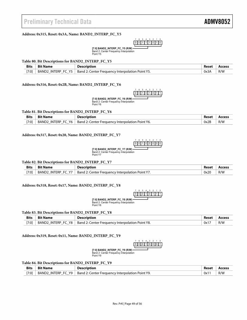
Preliminary Technical Data ADMV8052
Rev. PrK | Page 49 of 56
Address: 0x315, Reset: 0x3A, Name: BAND2_INTERP_FC_Y5
Table 80. Bit Descriptions for BAND2_INTERP_FC_Y5 Bits Bit Name Description Reset Access [7:0] BAND2_INTERP_FC_Y5 Band 2: Center Frequency Interpolation Point Y5. 0x3A R/W
Address: 0x316, Reset: 0x2B, Name: BAND2_INTERP_FC_Y6
Table 81. Bit Descriptions for BAND2_INTERP_FC_Y6 Bits Bit Name Description Reset Access [7:0] BAND2_INTERP_FC_Y6 Band 2: Center Frequency Interpolation Point Y6. 0x2B R/W
Address: 0x317, Reset: 0x20, Name: BAND2_INTERP_FC_Y7
Table 82. Bit Descriptions for BAND2_INTERP_FC_Y7 Bits Bit Name Description Reset Access [7:0] BAND2_INTERP_FC_Y7 Band 2: Center Frequency Interpolation Point Y7. 0x20 R/W
Address: 0x318, Reset: 0x17, Name: BAND2_INTERP_FC_Y8
Table 83. Bit Descriptions for BAND2_INTERP_FC_Y8 Bits Bit Name Description Reset Access [7:0] BAND2_INTERP_FC_Y8 Band 2: Center Frequency Interpolation Point Y8. 0x17 R/W
Address: 0x319, Reset: 0x11, Name: BAND2_INTERP_FC_Y9
Table 84. Bit Descriptions for BAND2_INTERP_FC_Y9 Bits Bit Name Description Reset Access [7:0] BAND2_INTERP_FC_Y9 Band 2: Center Frequency Interpolation Point Y9. 0x11 R/W
Band 2: Center Frequency InterpolationPoint Y5
0
01
12
03
14
15
16
07
0
[7:0] BAND2_INTERP_FC_Y5 (R/W)
Band 2: Center Frequency InterpolationPoint Y6
0
11
12
03
14
05
16
07
0
[7:0] BAND2_INTERP_FC_Y6 (R/W)
Band 2: Center Frequency InterpolationPoint Y7
0
01
02
03
04
05
16
07
0
[7:0] BAND2_INTERP_FC_Y7 (R/W)
Band 2: Center Frequency InterpolationPoint Y8
0
11
12
13
04
15
06
07
0
[7:0] BAND2_INTERP_FC_Y8 (R/W)
Band 2: Center Frequency InterpolationPoint Y9
0
11
02
03
04
15
06
07
0
[7:0] BAND2_INTERP_FC_Y9 (R/W)

ADMV8052 Preliminary Technical Data
Rev. PrK | Page 50 of 56
Address: 0x31A, Reset: 0x06, Name: BAND2_INTERP_BW_V0
Table 85. Bit Descriptions for BAND2_INTERP_BW_V0 Bits Bit Name Description Reset Access [7:0] BAND2_INTERP_BW_V0 Band 2: Bandwidth Interpolation Point V0. 0x6 R/W
Address: 0x31B, Reset: 0x13, Name: BAND2_INTERP_BW_V1
Table 86. Bit Descriptions for BAND2_INTERP_BW_V1 Bits Bit Name Description Reset Access [7:0] BAND2_INTERP_BW_V1 Band 2: Bandwidth Interpolation Point V1. 0x13 R/W
Address: 0x31C, Reset: 0x5E, Name: BAND2_INTERP_BW_V2
Table 87. Bit Descriptions for BAND2_INTERP_BW_V2 Bits Bit Name Description Reset Access [7:0] BAND2_INTERP_BW_V2 Band 2: Bandwidth Interpolation Point V2. 0x5E R/W
Band 2: Bandwidth Interpolation Point V0
0
01
12
13
04
05
06
07
0
[7:0] BAND2_INTERP_BW_V0 (R/W)
Band 2: Bandwidth Interpolation Point V1
0
11
12
03
04
15
06
07
0
[7:0] BAND2_INTERP_BW_V1 (R/W)
Band 2: Bandwidth Interpolation Point V2
0
01
12
13
14
15
06
17
0
[7:0] BAND2_INTERP_BW_V2 (R/W)

Preliminary Technical Data ADMV8052
Rev. PrK | Page 51 of 56
Address: 0x31D, Reset: 0x08, Name: BAND2_INTERP_MATCH_T0
Table 88. Bit Descriptions for BAND2_INTERP_MATCH_T0 Bits Bit Name Description Reset Access [7:0] BAND2_INTERP_MATCH_T0 Band 2: Match Interpolation Point T0. 0x8 R/W
Address: 0x31E, Reset: 0x21, Name: BAND2_INTERP_MATCH_T1
Table 89. Bit Descriptions for BAND2_INTERP_MATCH_T1 Bits Bit Name Description Reset Access [7:0] BAND2_INTERP_MATCH_T1 Band 2: Match Interpolation Point T1. 0x21 R/W
Address: 0x31F, Reset: 0x8C, Name: BAND2_INTERP_MATCH_T2
Table 90. Bit Descriptions for BAND2_INTERP_MATCH_T2 Bits Bit Name Description Reset Access [7:0] BAND2_INTERP_MATCH_T2 Band 2: Match Interpolation Point T2. 0x8C R/W
Band 2: Match Interpolation Point T0
0
01
02
03
14
05
06
07
0
[7:0] BAND2_INTERP_MATCH_T0 (R/W)
Band 2: Match Interpolation Point T1
0
11
02
03
04
05
16
07
0
[7:0] BAND2_INTERP_MATCH_T1 (R/W)
Band 2: Match Interpolation Point T2
0
01
02
13
14
05
06
07
1
[7:0] BAND2_INTERP_MATCH_T2 (R/W)

ADMV8052 Preliminary Technical Data
Rev. PrK | Page 52 of 56
Address: 0x320, Reset: 0xB9, Name: BAND3_INTERP_FC_Y0
Table 91. Bit Descriptions for BAND3_INTERP_FC_Y0 Bits Bit Name Description Reset Access [7:0] BAND3_INTERP_FC_Y0 Band 3: Center Frequency Interpolation Point Y0. 0xB9 R/W
Address: 0x321, Reset: 0x97, Name: BAND3_INTERP_FC_Y1
Table 92. Bit Descriptions for BAND3_INTERP_FC_Y1 Bits Bit Name Description Reset Access [7:0] BAND3_INTERP_FC_Y1 Band 3: Center Frequency Interpolation Point Y1. 0x97 R/W
Address: 0x322, Reset: 0x7C, Name: BAND3_INTERP_FC_Y2
Table 93. Bit Descriptions for BAND3_INTERP_FC_Y2 Bits Bit Name Description Reset Access [7:0] BAND3_INTERP_FC_Y2 Band 3: Center Frequency Interpolation Point Y2. 0x7C R/W
Address: 0x323, Reset: 0x55, Name: BAND3_INTERP_FC_Y3
Table 94. Bit Descriptions for BAND3_INTERP_FC_Y3 Bits Bit Name Description Reset Access [7:0] BAND3_INTERP_FC_Y3 Band 3: Center Frequency Interpolation Point Y3. 0x55 R/W
Address: 0x324, Reset: 0x3B, Name: BAND3_INTERP_FC_Y4
Table 95. Bit Descriptions for BAND3_INTERP_FC_Y4 Bits Bit Name Description Reset Access [7:0] BAND3_INTERP_FC_Y4 Band 3: Center Frequency Interpolation Point Y4. 0x3B R/W
Band 3: Center Frequency InterpolationPoint Y0
0
11
02
03
14
15
16
07
1
[7:0] BAND3_INTERP_FC_Y0 (R/W)
Band 3: Center Frequency InterpolationPoint Y1
0
11
12
13
04
15
06
07
1
[7:0] BAND3_INTERP_FC_Y1 (R/W)
Band 3: Center Frequency InterpolationPoint Y2
0
01
02
13
14
15
16
17
0
[7:0] BAND3_INTERP_FC_Y2 (R/W)
Band 3: Center Frequency InterpolationPoint Y3
0
11
02
13
04
15
06
17
0
[7:0] BAND3_INTERP_FC_Y3 (R/W)
Band 3: Center Frequency InterpolationPoint Y4
0
11
12
03
14
15
16
07
0
[7:0] BAND3_INTERP_FC_Y4 (R/W)

Preliminary Technical Data ADMV8052
Rev. PrK | Page 53 of 56
Address: 0x325, Reset: 0x28, Name: BAND3_INTERP_FC_Y5
Table 96. Bit Descriptions for BAND3_INTERP_FC_Y5 Bits Bit Name Description Reset Access [7:0] BAND3_INTERP_FC_Y5 Band 3: Center Frequency Interpolation Point Y5. 0x28 R/W
Address: 0x326, Reset: 0x1B, Name: BAND3_INTERP_FC_Y6
Table 97. Bit Descriptions for BAND3_INTERP_FC_Y6 Bits Bit Name Description Reset Access [7:0] BAND3_INTERP_FC_Y6 Band 3: Center Frequency Interpolation Point Y6. 0x1B R/W
Address: 0x327, Reset: 0x11, Name: BAND3_INTERP_FC_Y7
Table 98. Bit Descriptions for BAND3_INTERP_FC_Y7 Bits Bit Name Description Reset Access [7:0] BAND3_INTERP_FC_Y7 Band 3: Center Frequency Interpolation Point Y7. 0x11 R/W
Address: 0x328, Reset: 0x09, Name: BAND3_INTERP_FC_Y8
Table 99. Bit Descriptions for BAND3_INTERP_FC_Y8 Bits Bit Name Description Reset Access [7:0] BAND3_INTERP_FC_Y8 Band 3: Center Frequency Interpolation Point Y8. 0x9 R/W
Address: 0x329, Reset: 0x03, Name: BAND3_INTERP_FC_Y9
Table 100. Bit Descriptions for BAND3_INTERP_FC_Y9 Bits Bit Name Description Reset Access [7:0] BAND3_INTERP_FC_Y9 Band 3: Center Frequency Interpolation Point Y9. 0x3 R/W
Band 3: Center Frequency InterpolationPoint Y5
0
01
02
03
14
05
16
07
0
[7:0] BAND3_INTERP_FC_Y5 (R/W)
Band 3: Center Frequency InterpolationPoint Y6
0
11
12
03
14
15
06
07
0
[7:0] BAND3_INTERP_FC_Y6 (R/W)
Band 3: Center Frequency InterpolationPoint Y7
0
11
02
03
04
15
06
07
0
[7:0] BAND3_INTERP_FC_Y7 (R/W)
Band 3: Center Frequency InterpolationPoint Y8
0
11
02
03
14
05
06
07
0
[7:0] BAND3_INTERP_FC_Y8 (R/W)
Band 3: Center Frequency InterpolationPoint Y9
0
11
12
03
04
05
06
07
0
[7:0] BAND3_INTERP_FC_Y9 (R/W)

ADMV8052 Preliminary Technical Data
Rev. PrK | Page 54 of 56
Address: 0x32A, Reset: 0x10, Name: BAND3_INTERP_BW_V0
Table 101. Bit Descriptions for BAND3_INTERP_BW_V0 Bits Bit Name Description Reset Access [7:0] BAND3_INTERP_BW_V0 Band 3: Bandwidth Interpolation Point V0. 0x10 R/W
Address: 0x32B, Reset: 0x1F, Name: BAND3_INTERP_BW_V1
Table 102. Bit Descriptions for BAND3_INTERP_BW_V1 Bits Bit Name Description Reset Access [7:0] BAND3_INTERP_BW_V1 Band 3: Bandwidth Interpolation Point V1. 0x1F R/W
Address: 0x32C, Reset: 0x85, Name: BAND3_INTERP_BW_V2
Table 103. Bit Descriptions for BAND3_INTERP_BW_V2 Bits Bit Name Description Reset Access [7:0] BAND3_INTERP_BW_V2 Band 3: Bandwidth Interpolation Point V2. 0x85 R/W
Band 3: Bandwidth Interpolation Point V0
0
01
02
03
04
15
06
07
0
[7:0] BAND3_INTERP_BW_V0 (R/W)
Band 3: Bandwidth Interpolation Point V1
0
11
12
13
14
15
06
07
0
[7:0] BAND3_INTERP_BW_V1 (R/W)
Band 3: Bandwidth Interpolation Point V2
0
11
02
13
04
05
06
07
1
[7:0] BAND3_INTERP_BW_V2 (R/W)

Preliminary Technical Data ADMV8052
Rev. PrK | Page 55 of 56
Address: 0x32D, Reset: 0x13, Name: BAND3_INTERP_MATCH_T0
Table 104. Bit Descriptions for BAND3_INTERP_MATCH_T0 Bits Bit Name Description Reset Access [7:0] BAND3_INTERP_MATCH_T0 Band 3: Match Interpolation Point T0. 0x13 R/W
Address: 0x32E, Reset: 0x2A, Name: BAND3_INTERP_MATCH_T1
Table 105. Bit Descriptions for BAND3_INTERP_MATCH_T1 Bits Bit Name Description Reset Access [7:0] BAND3_INTERP_MATCH_T1 Band 3: Match Interpolation Point T1. 0x2A R/W
Address: 0x32F, Reset: 0xA2, Name: BAND3_INTERP_MATCH_T2
Table 106. Bit Descriptions for BAND3_INTERP_MATCH_T2 Bits Bit Name Description Reset Access [7:0] BAND3_INTERP_MATCH_T2 Band 3: Match Interpolation Point T2. 0xA2 R/W
Band 3: Match Interpolation Point T0
0
11
12
03
04
15
06
07
0
[7:0] BAND3_INTERP_MATCH_T0 (R/W)
Band 3: Match Interpolation Point T1
0
01
12
03
14
05
16
07
0
[7:0] BAND3_INTERP_MATCH_T1 (R/W)
Band 3: Match Interpolation Point T2
0
01
12
03
04
05
16
07
1
[7:0] BAND3_INTERP_MATCH_T2 (R/W)

ADMV8052 Preliminary Technical Data
Rev. PrK | Page 56 of 56
OUTLINE DIMENSIONS
Figure 24. Land Grid Array Package [LGA]
22 mm × 22 mm Body and 5.73 mm Package Height (CC-32-8)
Dimensions shown in millimeters
©2021 Analog Devices, Inc. All rights reserved. Trademarks and registered trademarks are the property of their respective owners. D16902-1/21(PrK)


![PVCPR11 Edital 3.5 GHz v03.ppt [Modo de Compatibilidade]...2011/06/09 · 35 MHz 35 MHz 10 MHz 10 MHz 10 MHz 10 MHz 10 MHz 10 MHz 3.400,00 MHz 3.600,00 MHz 10 MHz 35 MHz 10 MHz 10](https://img.dokumen.tips/doc/110x75/5f7286506e7f433bb4685297/pvcpr11-edital-35-ghz-v03ppt-modo-de-compatibilidade-20110609-35-mhz.jpg)