Embed Size (px)
Citation preview

FEATURES
DESCRIPTION
PCM3052A
SLES160–NOVEMBER 2005
24-BIT, 96-kHz STEREO AUDIO CODEC WITHMICROPHONE AMPLIFIER, BIAS, MUXTIPLEXER, AND PGA
• Multiple Functions With I2C Interface:• Microphone Amplifier and Bias – Digital De-Emphasis: 32-, 44.1-, 48-kHz
– Monaural Microphone Amplifier: 34-dB Gain – Zipper-Noise-Free Digital Attenuation andat Differential Input Soft Mute for DAC
– Microphone Bias: 1 mA at 3.75 V – HPF Bypass Control for ADC• Multiplexer and PGA – S/PDIF Output Control
– Multiplex of Stereo Single-Ended Line – Power Down: ADC/DAC IndependentlyInputs and Monaural Microphone Amplifier • External Power-Down Pin:
– 0.1 Vrms to 1.5 Vrms Full-Scale Input Range – ADC/DAC Simultaneously– 22-kΩ Input Resistance at 0.1-Vrms Input • Audio Data Format: 24-Bit I2S Only– 20 dB to –4 dB/range, 1 dB/step PGA • Sampling Rate:
• Reference Output: ±10 mA at 2.5 V – 16–96 kHz for Both ADC and DAC• 24-Bit Delta-Sigma ADC and DAC • System Clock: 256 fS Only• Stereo ADC: • Dual Power Supplies:
– Full-Scale Input: 3 Vp-p – 5 V for Analog and 3.3 V for Digital– Antialiasing Filter Included • Package: VQFN-32– 1/64 Decimation Filter:
• Pass-Band Ripple: ±0.05 dB• Stop-Band Attenuation: –65 dB The PCM3052A is a low-cost, single-chip, 24-bit
stereo audio codec (ADC and DAC) with– On-Chip High-Pass Filter: 0.91 Hz atsingle-ended analog voltage input and output. It alsofS = 48 kHzhas an analog front end consisting of a 34-dB– High Performance:microphone amplifier, microphone bias generator, 2
• THD+N: –94 dB (Typical) stereo multiplexers, and a wide-range PGA. Analog-to-digital converters (ADCs) employ delta-sigma• SNR: 101 dB (Typical)modulation with 64-times oversampling. On the other• Dynamic Range: 101 dB (Typical)hand, digital-to-analog converters (DACs) employ
• Stereo DAC: modulation with 64- and 128-times oversampling.ADCs include a digital decimation filter with a– Single-Ended Voltage Output: 4 Vp-phigh-pass filter, and DACs include an 8-times– Analog Low-Pass Filter Includedoversampling digital interpolation filter. The
– ×8 Oversampling Digital Filter: PCM3052A has many functions which are controlled• Pass-Band Ripple: ±0.03 dB using the I2C interface: DAC digital de-emphasis,
digital attenuation, soft mute etc. The PCM3052A• Stop-Band Attenuation: –50 dBalso has an S/PDIF output pin for the DAC digital
– High Performance: input. The power-down mode, which works on ADCs• THD+N: –97 dB (Typical) and DACs simultaneously, is provided by an external
pin. The PCM3052A is suitable for a wide variety of• SNR: 105 dB (Typical)cost-sensitive PC audio (recorder and player)• Dynamic Range: 104 dB (Typical) applications where good performance is required.
• S/PDIF Output for DAC Digital Input The PCM3052A is fabricated using a highly advancedA CMOS process and is available in a small 32-pin
VQFN package.
Please be aware that an important notice concerning availability, standard warranty, and use in critical applications of TexasInstruments semiconductor products and disclaimers thereto appears at the end of this data sheet.
System Two, Audio Precision are trademarks of Audio Precision, Inc.All trademarks are the property of their respective owners.
PRODUCTION DATA information is current as of publication date. Copyright © 2005, Texas Instruments IncorporatedProducts conform to specifications per the terms of the TexasInstruments standard warranty. Production processing does notnecessarily include testing of all parameters.

www.ti.com
ABSOLUTE MAXIMUM RATINGS
RECOMMENDED OPERATING CONDITIONS
PCM3052A
SLES160–NOVEMBER 2005
This integrated circuit can be damaged by ESD. Texas Instruments recommends that all integratedcircuits be handled with appropriate precautions. Failure to observe proper handling and installationprocedures can cause damage.
ESD damage can range from subtle performance degradation to complete device failure. Precisionintegrated circuits may be more susceptible to damage because very small parametric changes couldcause the device not to meet its published specifications.
over operating free-air temperature range (unless otherwise noted) (1)
PCM3052A
VCC1, VCC2, VCC3 –0.3 V to 6.5 VSupply voltage
VDD –0.3 V to 4 V
Supply voltage differences VCC1, VCC2, VCC3 ±0.1 V
Ground voltage differences AGND1, AGND2, AGND3, DGND ±0.1 V
PDWN, DIN, SCKI, SDA, SCL, ADR, I2CEN –0.3 V to 6.5 VDigital input voltage
DOUT, LRCK, BCK, DOUTS – 0.3 V to (VDD + 0.3 V) < 4 V
VINL, VINR, VREF1, VREF2, REFO, ATEST, L/M, VOUTR, VOUTL, VCOM, –0.3 V to (VCC + 0.3 V) < 6.5 VAnalog input voltage MINP, MINM, MBIAS
Input current (any pins except supplies) ±10 mA
Ambient temperature under bias –40°C to 125°C
Storage temperature –55°C to 150°C
Junction temperature 150°C
Lead temperature (soldering) 260°C, 5 s
Package temperature (reflow, peak) 260°C
(1) Stresses beyond those listed under absolute maximum ratings may cause permanent damage to the device. These are stress ratingsonly and functional operation of the device at these or any other conditions beyond those indicated under recommended operatingconditions is not implied. Exposure to absolute-maximum-rated conditions for extended periods may affect device reliability.
over operating free-air temperature range (unless otherwise noted)
MIN NOM MAX UNIT
VDD Digital supply voltage 3 3.3 3.6 V
VCC Analog supply voltage 4.5 5 5.5 V
Digital input logic family TTLcompatible
System clock 4 25 MHzDigital input clock frequency
Sampling clock 16 96 kHz
Line input, full scale, PGA = 0 dB 3 Vp-pAnalog input voltage
Microphone input, full scale, PGA = 0 dB 30 mVp-p
Digital output load capacitance 20 pF
Line output load resistance 5 kΩ
Line output load capacitance 50 pF
Microphone bias output load resistance 3.75 kΩ
Reference output load resistance 250 Ω
TA Operating free-air temperature –40 85 °C
2
www.ti.com
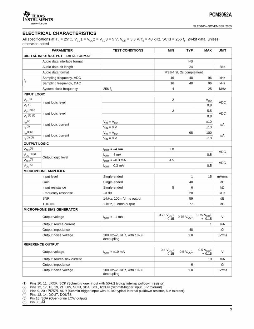
ELECTRICAL CHARACTERISTICS
PCM3052A
SLES160–NOVEMBER 2005
All specifications at TA = 25°C, VCC1 = VCC2 = VCC3 = 5 V, VDD = 3.3 V, fS = 48 kHz, SCKI = 256 fS, 24-bit data, unlessotherwise noted
PARAMETER TEST CONDITIONS MIN TYP MAX UNIT
DIGITAL INPUT/OUTPUT – DATA FORMAT
Audio data interface format I2S
Audio data bit length 24 Bits
Audio data format MSB-first, 2s complement
Sampling frequency, ADC 16 48 96 kHzfS
Sampling frequency, DAC 16 48 96 kHz
System clock frequency 256 fS 4 25 MHz
INPUT LOGIC
VIH(1) 2 VDD
Input logic level VDCVIL
(1) 0.8
VIH(2) (3) 2 5.5
Input logic level VDCVIL
(2) (3) 0.8
IIH(2) VIN = VDD ±10Input logic current µA
IIL(2) VIN = 0 V ±10
IIH(1)(3) VIN = VDD 65 100Input logic current µA
IIL(1) (3) VIN = 0 V ±10
OUTPUT LOGIC
VOH(4) IOUT = –4 mA 2.8
VDCVOL
(4) (5) IOUT = 4 mA 0.5Output logic level
VOH(6) IOUT = –0.3 mA 4.5
VDCVOL
(6) IOUT = 0.3 mA 0.5
MICROPHONE AMPLIFIER
Input level Single-ended 1 15 mVrms
Gain Single-ended 40 dB
Input resistance Single-ended 5 6 kΩ
Frequency response –3 dB 20 kHz
SNR 1-kHz, 100-mVrms output 59 dB
THD+N 1-kHz, 1-Vrms output –77 dB
MICROPHONE BIAS GENERATOR
0.75 VCC1 0.75 VCC1Output voltage IOUT = –1 mA 0.75 VCC1 V– 0.15 + 0.15
Output source current 1 mA
Output impedance 48 Ω
Output noise voltage 100 Hz–20 kHz, with 10-µF 1.8 µVrmsdecoupling
REFERENCE OUTPUT
0.5 VCC1 0.5 VCC1Output voltage IOUT = ±10 mA 0.5 VCC1 V– 0.15 + 0.15
Output source/sink current 10 mA
Output impedance 6 Ω
Output noise voltage 100 Hz–20 kHz, with 10-µF 1.8 µVrmsdecoupling
(1) Pins 10, 11: LRCK, BCK (Schmitt-trigger input with 50-kΩ typical internal pulldown resistor)(2) Pins 12, 17, 18, 19, 21: DIN, SCKI, SDA, SCL, I2CEN (Schmitt-trigger input, 5-V tolerant)(3) Pins 9, 20 : PDWN, ADR (Schmitt-trigger input with 50-kΩ typical internal pulldown resistor, 5-V tolerant).(4) Pins 13, 14: DOUT, DOUTS(5) Pin 18: SDA (Open-drain LOW output)(6) Pin 3: L/M
3
www.ti.com
PCM3052A
SLES160–NOVEMBER 2005
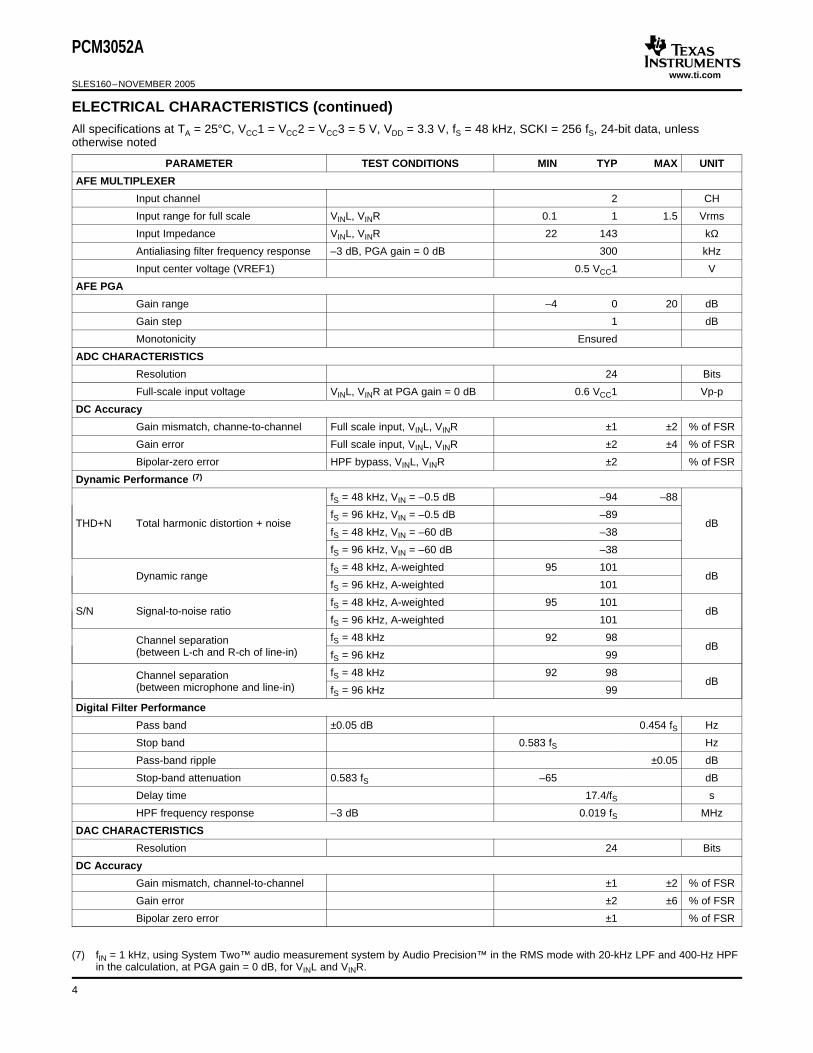
ELECTRICAL CHARACTERISTICS (continued)All specifications at TA = 25°C, VCC1 = VCC2 = VCC3 = 5 V, VDD = 3.3 V, fS = 48 kHz, SCKI = 256 fS, 24-bit data, unlessotherwise noted
PARAMETER TEST CONDITIONS MIN TYP MAX UNIT
AFE MULTIPLEXER
Input channel 2 CH
Input range for full scale VINL, VINR 0.1 1 1.5 Vrms
Input Impedance VINL, VINR 22 143 kΩ
Antialiasing filter frequency response –3 dB, PGA gain = 0 dB 300 kHz
Input center voltage (VREF1) 0.5 VCC1 V
AFE PGA
Gain range –4 0 20 dB
Gain step 1 dB
Monotonicity Ensured
ADC CHARACTERISTICS
Resolution 24 Bits
Full-scale input voltage VINL, VINR at PGA gain = 0 dB 0.6 VCC1 Vp-p
DC Accuracy
Gain mismatch, channe-to-channel Full scale input, VINL, VINR ±1 ±2 % of FSR
Gain error Full scale input, VINL, VINR ±2 ±4 % of FSR
Bipolar-zero error HPF bypass, VINL, VINR ±2 % of FSR
Dynamic Performance (7)
fS = 48 kHz, VIN = –0.5 dB –94 –88
fS = 96 kHz, VIN = –0.5 dB –89THD+N Total harmonic distortion + noise dB
fS = 48 kHz, VIN = –60 dB –38
fS = 96 kHz, VIN = –60 dB –38
fS = 48 kHz, A-weighted 95 101Dynamic range dB
fS = 96 kHz, A-weighted 101
fS = 48 kHz, A-weighted 95 101S/N Signal-to-noise ratio dB
fS = 96 kHz, A-weighted 101
fS = 48 kHz 92 98Channel separation dB(between L-ch and R-ch of line-in) fS = 96 kHz 99
fS = 48 kHz 92 98Channel separation dB(between microphone and line-in) fS = 96 kHz 99
Digital Filter Performance
Pass band ±0.05 dB 0.454 fS Hz
Stop band 0.583 fS Hz
Pass-band ripple ±0.05 dB
Stop-band attenuation 0.583 fS –65 dB
Delay time 17.4/fS s
HPF frequency response –3 dB 0.019 fS MHz
DAC CHARACTERISTICS
Resolution 24 Bits
DC Accuracy
Gain mismatch, channel-to-channel ±1 ±2 % of FSR
Gain error ±2 ±6 % of FSR
Bipolar zero error ±1 % of FSR
(7) fIN = 1 kHz, using System Two™ audio measurement system by Audio Precision™ in the RMS mode with 20-kHz LPF and 400-Hz HPFin the calculation, at PGA gain = 0 dB, for VINL and VINR.
4

www.ti.com
PCM3052A
SLES160–NOVEMBER 2005
ELECTRICAL CHARACTERISTICS (continued)All specifications at TA = 25°C, VCC1 = VCC2 = VCC3 = 5 V, VDD = 3.3 V, fS = 48 kHz, SCKI = 256 fS, 24-bit data, unlessotherwise noted
PARAMETER TEST CONDITIONS MIN TYP MAX UNIT
Dynamic Performance (8)
fS = 48 kHz, VOUT = 0 dB –97 –90
fS = 96 kHz, VOUT = 0 dB –99THD+N Total harmonic distortion + noise dB
fS = 48 kHz, VOUT = –60 dB –42
fS = 96 kHz, VOUT = –60 dB –43
fS = 48 kHz, EIAJ, A-weighted 98 104Dynamic range dB
fS = 96 kHz, EIAJ, A-weighted 106
fS = 48 kHz, EIAJ, A-weighted 99 105S/N Signal-to-noise ratio dB
fS = 96 kHz, EIAJ, A-weighted 106
fS = 48 kHz 97 103Channel separation dB
fS = 96 kHz 104
Analog Output
Output voltage 0.8 VCC2 Vp-p
Center voltage 0.5 VCC2 V
Load impedance AC coupling 5 kΩ
f = 20 kHz –0.03LPF frequency response dB
f = 40 kHz –0.20
Digital Filter Performance
Pass band ±0.03 dB 0.454 fS Hz
Stop band 0.546 fS Hz
Pass-band ripple ±0.03 dB
Stop-band attenuation 0.546 fS –50 dB
Delay time 20/fS s
De-emphasis error ±0.1 dB
POWER SUPPLY REQUIREMENTS
VCC1VCC2 4.25 5 5.5
Voltage range VDCVCC3
VDD 3 3.3 3.6
fS = 48 kHz 39 50mA
ICC(9) fS = 96 kHz 41
Full power down (10) 300 µASupply current
fS = 48 kHz 10 15mA
IDD fS = 96 kHz 19
Full power down (10) 90 µA
Operation, fS = 48 kHz 228 300
Operation, fS = 96 kHz 268
ADC operation at fS = 48 180Power dissipation kHz/DAC power down mW
ADC power down/DAC operation 63at fS = 48 kHz
Full power down (10) 1.8
(8) fOUT = 1 kHz, using System Two audio measurement system by Audio Precision in the RMS mode with 20-kHz LPF and 400-Hz HPF.(9) ICC = ICC1 + ICC2 + ICC3(10) Halt SCKI, BCK, LRCK.
5
www.ti.com
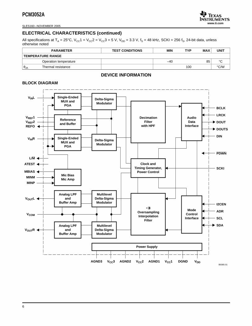
DEVICE INFORMATION
Single-EndedMUX and
PGA
LRCK
VINL
Referenceand Buffer
VREF1VREF2
VINR
Delta-SigmaModulator
DecimationFilter
with HPF
Power Supply
VCC3AGND3 VCC2AGND2
Clock andTiming Generator,
Power Control
AudioData
InterfaceDOUT
Delta-SigmaModulator
DOUTS
DIN
Analog LPFand
Buffer AmpVOUTL
VCOM
VOUTR
MultilevelDelta-SigmaModulator
× 8OversamplingInterpolation
Filter
ModeControlInterface
I2CEN
MultilevelDelta-SigmaModulator
ADR
SCL
SDAAnalog LPFand
Buffer Amp
AGND1
SCKI
PDWN
REFO
VDDDGNDVCC1
BCLK
Mic BiasMic Amp
MINM
MBIAS
MINP
ATEST
L/M
B0085-01
Single-EndedMUX and
PGA
PCM3052A
SLES160–NOVEMBER 2005
ELECTRICAL CHARACTERISTICS (continued)All specifications at TA = 25°C, VCC1 = VCC2 = VCC3 = 5 V, VDD = 3.3 V, fS = 48 kHz, SCKI = 256 fS, 24-bit data, unlessotherwise noted
PARAMETER TEST CONDITIONS MIN TYP MAX UNIT
TEMPERATURE RANGE
Operation temperature –40 85 °C
θJA Thermal resistance 100 °C/W
BLOCK DIAGRAM
6
www.ti.com
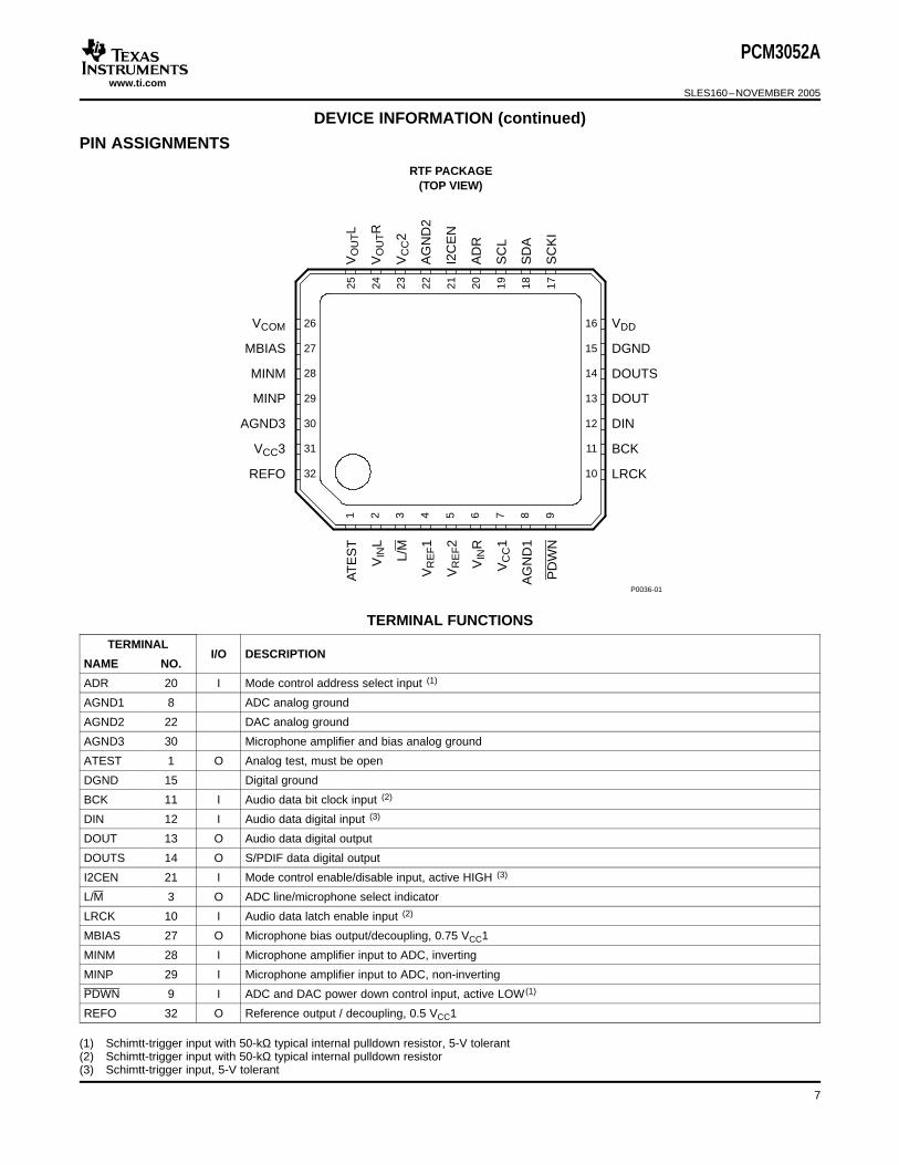
PIN ASSIGNMENTS
VCOM
MBIAS
MINM
MINP
AGND3
VCC3
REFO
VDD
DGND
DOUTS
DOUT
DIN
BCK
LRCK
RTF PACKAGE(TOP VIEW)
P0036-01
26
27
28
29
30
31
32
16
15
14
13
12
11
10
AT
ES
T
VIN
L
L/M
VR
EF1
VR
EF2
VIN
R
VC
C1
AG
ND
1
PD
WN
1 2 3 4 5 6 7 8 9
VO
UTL
VO
UTR
VC
C2
AG
ND
2
I2C
EN
AD
R
SC
L
SD
A
SC
KI
25 24 23 22 21 20 19 18 17
PCM3052A
SLES160–NOVEMBER 2005
DEVICE INFORMATION (continued)
TERMINAL FUNCTIONS
TERMINALI/O DESCRIPTION
NAME NO.
ADR 20 I Mode control address select input (1)
AGND1 8 ADC analog ground
AGND2 22 DAC analog ground
AGND3 30 Microphone amplifier and bias analog ground
ATEST 1 O Analog test, must be open
DGND 15 Digital ground
BCK 11 I Audio data bit clock input (2)
DIN 12 I Audio data digital input (3)
DOUT 13 O Audio data digital output
DOUTS 14 O S/PDIF data digital output
I2CEN 21 I Mode control enable/disable input, active HIGH (3)
L/M 3 O ADC line/microphone select indicator
LRCK 10 I Audio data latch enable input (2)
MBIAS 27 O Microphone bias output/decoupling, 0.75 VCC1
MINM 28 I Microphone amplifier input to ADC, inverting
MINP 29 I Microphone amplifier input to ADC, non-inverting
PDWN 9 I ADC and DAC power down control input, active LOW (1)
REFO 32 O Reference output / decoupling, 0.5 VCC1
(1) Schimtt-trigger input with 50-kΩ typical internal pulldown resistor, 5-V tolerant(2) Schimtt-trigger input with 50-kΩ typical internal pulldown resistor(3) Schimtt-trigger input, 5-V tolerant
7

www.ti.com
TYPICAL PERFORMANCE CURVES OF INTERNAL FILTER (ADC SECTION)
DIGITAL FILTER
Normalized Frequency [×fS]
−200
−150
−100
−50
0
0 8 16 24 32
Am
plit
ud
e −
dB
G001Normalized Frequency [×fS]
−100
−80
−60
−40
−20
0
0.0 0.2 0.4 0.6 0.8 1.0
Am
plit
ud
e −
dB
G002
PCM3052A
SLES160–NOVEMBER 2005
DEVICE INFORMATION (continued)
TERMINAL FUNCTIONS (continued)
TERMINALI/O DESCRIPTION
NAME NO.
SCKI 17 I System clock input, 256 fS(3)
SCL 19 I Mode control clock input (3)
SDA 18 I/O Mode control data input/output (4)
VCC1 7 ADC analog power supply, 5 V
VCC2 23 DAC analog power supply, 5 V
VCC3 31 Microphone amplifier and bias analog power supply, 5 V
VCOM 26 DAC common voltage decoupling, 0.5 VCC2
VDD 16 Digital power supply, 3.3 V
VINL 2 I Line input to ADC, L-channel
VINR 6 I Line input to ADC, R-channel
VOUTL 25 O Analog output from DAC, L-channel
VOUTR 24 O Analog output from DAC, R-channel
VREF1 4 ADC reference 1 voltage output, 0.5 VCC1
VREF2 5 ADC reference 2 voltage decoupling, VCC1
(4) Schimtt-trigger input/open-drain LOW output, 5-V tolerant
All specifications at TA = 25°C, VCC1 = VCC2 = VCC3 = 5 V, VDD = 3.3 V, fS = 48 kHz, SCKI = 256fS, 24-bit data, unlessotherwise noted.
OVERALL CHARACTERISTICS STOP-BAND ATTENUATION CHARACTERISTICS
Figure 1. Figure 2.
8

www.ti.com
Normalized Frequency [×fS]
−1.0
−0.8
−0.6
−0.4
−0.2
0.0
0.2
0.0 0.1 0.2 0.3 0.4 0.5
Am
plit
ud
e −
dB
G003Normalized Frequency [×fS]
−10
−9
−8
−7
−6
−5
−4
−3
−2
−1
0
0.45 0.47 0.49 0.51 0.53 0.55
Am
plit
ud
e −
dB
G004
−4.13 dB at 0.5 fS
Normalized Frequency [×fS/1000]
−1.0
−0.8
−0.6
−0.4
−0.2
0.0
0.2
0 1 2 3 4
Am
plit
ud
e −
dB
G006Normalized Frequency [×fS/1000]
−100
−90
−80
−70
−60
−50
−40
−30
−20
−10
0
0.0 0.1 0.2 0.3 0.4 0.5
Am
plit
ud
e −
dB
G005
PCM3052A
SLES160–NOVEMBER 2005
TYPICAL PERFORMANCE CURVES OF INTERNAL FILTER (ADC SECTION) (continued)All specifications at TA = 25°C, VCC1 = VCC2 = VCC3 = 5 V, VDD = 3.3 V, fS = 48 kHz, SCKI = 256fS, 24-bit data, unlessotherwise noted.
PASS-BAND RIPPLE CHARACTERISTICS TRANSITION BAND CHARACTERISTICS
Figure 3. Figure 4.
HIGH-PASS FILTER STOP-BAND CHARACTERISTICS HIGH-PASS FILTER PASS-BAND CHARACTERISTICS
Figure 5. Figure 6.
9
www.ti.com
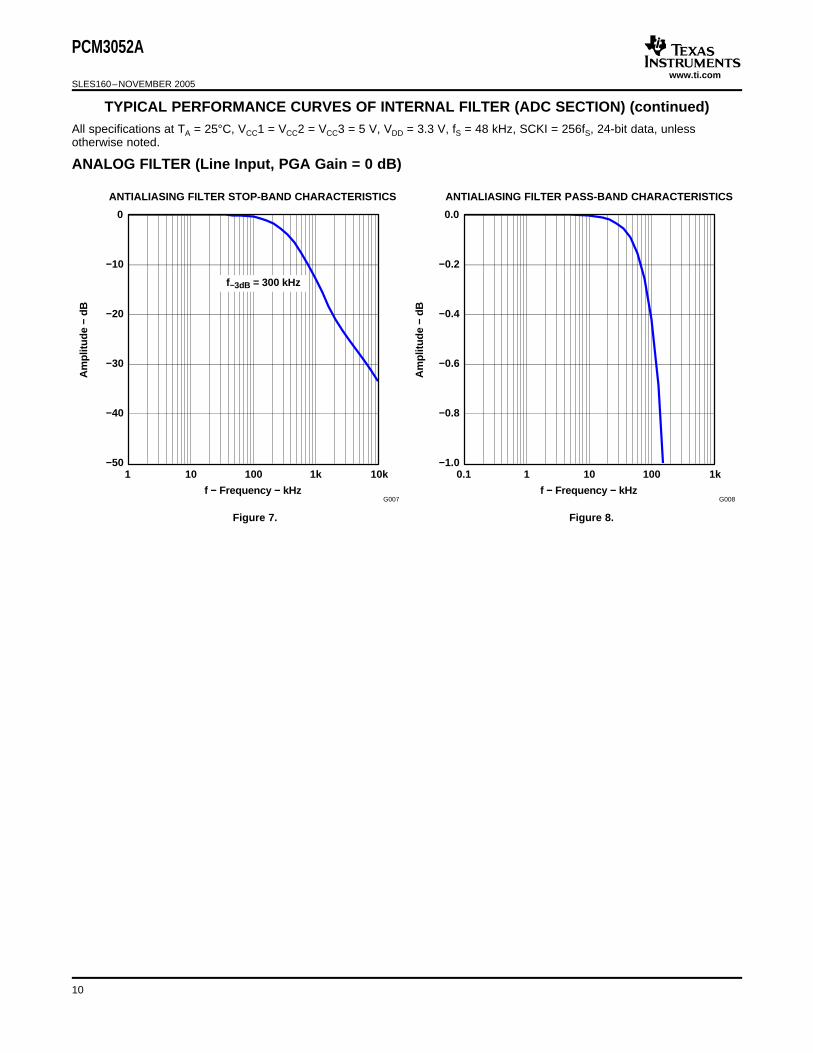
ANALOG FILTER (Line Input, PGA Gain = 0 dB)
−50
−40
−30
−20
−10
0
f − Frequency − kHz
Am
plit
ud
e −
dB
1 10 100 10k1k
G007
f−3dB = 300 kHz
−1.0
−0.8
−0.6
−0.4
−0.2
0.0
f − Frequency − kHz
Am
plit
ud
e −
dB
0.1 1 100 1k
G008
10
PCM3052A
SLES160–NOVEMBER 2005
TYPICAL PERFORMANCE CURVES OF INTERNAL FILTER (ADC SECTION) (continued)All specifications at TA = 25°C, VCC1 = VCC2 = VCC3 = 5 V, VDD = 3.3 V, fS = 48 kHz, SCKI = 256fS, 24-bit data, unlessotherwise noted.
ANTIALIASING FILTER STOP-BAND CHARACTERISTICS ANTIALIASING FILTER PASS-BAND CHARACTERISTICS
Figure 7. Figure 8.
10
www.ti.com
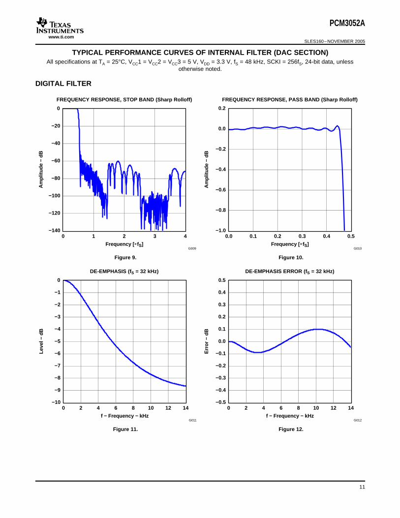
TYPICAL PERFORMANCE CURVES OF INTERNAL FILTER (DAC SECTION)
DIGITAL FILTER
−140
−120
−100
−80
−60
−40
−20
0
0 1 2 3 4
Am
plit
ud
e −
dB
Frequency [×fS]G009
−1.0
−0.8
−0.6
−0.4
−0.2
0.0
0.2
0.0 0.1 0.2 0.3 0.4 0.5
Am
plit
ud
e −
dB
Frequency [×fS]G010
−10
−9
−8
−7
−6
−5
−4
−3
−2
−1
0
0 2 4 6 8 10 12 14
Lev
el −
dB
f − Frequency − kHzG011
−0.5
−0.4
−0.3
−0.2
−0.1
0.0
0.1
0.2
0.3
0.4
0.5
0 2 4 6 8 10 12 14
Err
or
− d
B
f − Frequency − kHzG012
PCM3052A
SLES160–NOVEMBER 2005
All specifications at TA = 25°C, VCC1 = VCC2 = VCC3 = 5 V, VDD = 3.3 V, fS = 48 kHz, SCKI = 256fS, 24-bit data, unlessotherwise noted.
FREQUENCY RESPONSE, STOP BAND (Sharp Rolloff) FREQUENCY RESPONSE, PASS BAND (Sharp Rolloff)
Figure 9. Figure 10.
DE-EMPHASIS (fS = 32 kHz) DE-EMPHASIS ERROR (fS = 32 kHz)
Figure 11. Figure 12.
11

www.ti.com
−10
−9
−8
−7
−6
−5
−4
−3
−2
−1
0
0 2 4 6 8 10 12 14 16 18 20
Lev
el −
dB
f − Frequency − kHzG013
−0.5
−0.4
−0.3
−0.2
−0.1
0.0
0.1
0.2
0.3
0.4
0.5
0 2 4 6 8 10 12 14 16 18 20
Err
or
− d
B
f − Frequency − kHzG014
−10
−9
−8
−7
−6
−5
−4
−3
−2
−1
0
0 2 4 6 8 10 12 14 16 18 20 22
Lev
el −
dB
f − Frequency − kHzG015
−0.5
−0.4
−0.3
−0.2
−0.1
0.0
0.1
0.2
0.3
0.4
0.5
0 2 4 6 8 10 12 14 16 18 20 22
Err
or
− d
B
f − Frequency − kHzG016
PCM3052A
SLES160–NOVEMBER 2005
TYPICAL PERFORMANCE CURVES OF INTERNAL FILTER (DAC SECTION) (continued)All specifications at TA = 25°C, VCC1 = VCC2 = VCC3 = 5 V, VDD = 3.3 V, fS = 48 kHz, SCKI = 256fS, 24-bit data, unlessotherwise noted.
DE-EMPHASIS (fS = 44.1 kHz) DE-EMPHASIS ERROR (fS = 44.1 kHz)
Figure 13. Figure 14.
DE-EMPHASIS (fS = 48 kHz) DE-EMPHASIS ERROR (fS = 48 kHz)
Figure 15. Figure 16.
12

www.ti.com
ANALOG FILTER
−50
−40
−30
−20
−10
0
f − Frequency − kHz
Am
plit
ud
e −
dB
1 10 100 10k1k
G017
f−3dB = 300 kHz
−1.0
−0.8
−0.6
−0.4
−0.2
0.0
f − Frequency − kHz
Am
plit
ud
e −
dB
0.1 1 100 1k
G018
10
PCM3052A
SLES160–NOVEMBER 2005
TYPICAL PERFORMANCE CURVES OF INTERNAL FILTER (DAC SECTION) (continued)All specifications at TA = 25°C, VCC1 = VCC2 = VCC3 = 5 V, VDD = 3.3 V, fS = 48 kHz, SCKI = 256fS, 24-bit data, unlessotherwise noted.
STOP-BAND CHARACTERISTICS (1 kHz–10 MHz) PASS-BAND CHARACTERISTICS (100 Hz–1 MHz)
Figure 17. Figure 18.
13
www.ti.com
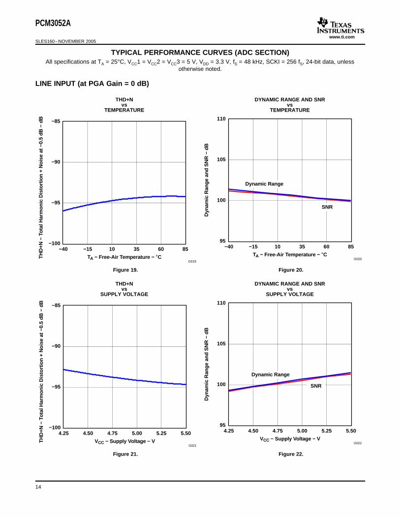
TYPICAL PERFORMANCE CURVES (ADC SECTION)
LINE INPUT (at PGA Gain = 0 dB)
95
100
105
110
−40 −15 10 35 60 85
Dyn
amic
Ran
ge
and
SN
R −
dB
TA − Free-Air Temperature − °CG020
SNR
Dynamic Range
−100
−95
−90
−85
−40 −15 10 35 60 85
TH
D+N
− T
ota
l Har
mo
nic
Dis
tort
ion
+ N
ois
e at
−0.
5 d
B −
dB
TA − Free-Air Temperature − °CG019
95
100
105
110
4.25 4.50 4.75 5.00 5.25 5.50
Dyn
amic
Ran
ge
and
SN
R −
dB
VCC − Supply Voltage − VG022
SNR
Dynamic Range
−100
−95
−90
−85
4.25 4.50 4.75 5.00 5.25 5.50
TH
D+N
− T
ota
l Har
mo
nic
Dis
tort
ion
+ N
ois
e at
−0.
5 d
B −
dB
VCC − Supply Voltage − VG021
PCM3052A
SLES160–NOVEMBER 2005
All specifications at TA = 25°C, VCC1 = VCC2 = VCC3 = 5 V, VDD = 3.3 V, fS = 48 kHz, SCKI = 256 fS, 24-bit data, unlessotherwise noted.
THD+N DYNAMIC RANGE AND SNRvs vs
TEMPERATURE TEMPERATURE
Figure 19. Figure 20.
THD+N DYNAMIC RANGE AND SNRvs vs
SUPPLY VOLTAGE SUPPLY VOLTAGE
Figure 21. Figure 22.
14

www.ti.com
95
100
105
110
32 48 64 80 96
fS − Sampling Frequency − kHzG024
Dyn
amic
Ran
ge
and
SN
R −
dB
SNR
Dynamic Range
−100
−95
−90
−85
32 48 64 80 96
TH
D+N
− T
ota
l Har
mo
nic
Dis
tort
ion
+ N
ois
e at
−0.
5 d
B −
dB
fS − Sampling Frequency − kHzG023
PCM3052A
SLES160–NOVEMBER 2005
TYPICAL PERFORMANCE CURVES (ADC SECTION) (continued)All specifications at TA = 25°C, VCC1 = VCC2 = VCC3 = 5 V, VDD = 3.3 V, fS = 48 kHz, SCKI = 256 fS, 24-bit data, unlessotherwise noted.
THD+N DYNAMIC RANGE AND SNRvs vs
SAMPLING FREQUENCY SAMPLING FREQUENCY
Figure 23. Figure 24.
15
www.ti.com
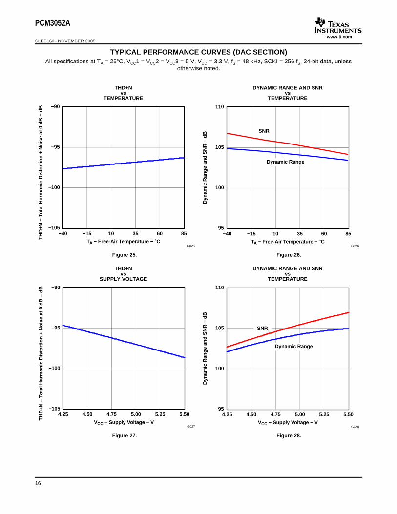
TYPICAL PERFORMANCE CURVES (DAC SECTION)
−105
−100
−95
−90
−40 −15 10 35 60 85
TH
D+N
− T
ota
l Har
mo
nic
Dis
tort
ion
+ N
ois
e at
0 d
B −
dB
TA − Free-Air Temperature − °CG025
95
100
105
110
−40 −15 10 35 60 85
Dyn
amic
Ran
ge
and
SN
R −
dB
TA − Free-Air Temperature − °CG026
SNR
Dynamic Range
−105
−100
−95
−90
4.25 4.50 4.75 5.00 5.25 5.50
TH
D+N
− T
ota
l Har
mo
nic
Dis
tort
ion
+ N
ois
e at
0 d
B −
dB
VCC − Supply Voltage − VG027
95
100
105
110
4.25 4.50 4.75 5.00 5.25 5.50
Dyn
amic
Ran
ge
and
SN
R −
dB
VCC − Supply Voltage − VG028
SNR
Dynamic Range
PCM3052A
SLES160–NOVEMBER 2005
All specifications at TA = 25°C, VCC1 = VCC2 = VCC3 = 5 V, VDD = 3.3 V, fS = 48 kHz, SCKI = 256 fS, 24-bit data, unlessotherwise noted.
THD+N DYNAMIC RANGE AND SNRvs vs
TEMPERATURE TEMPERATURE
Figure 25. Figure 26.
THD+N DYNAMIC RANGE AND SNRvs vs
SUPPLY VOLTAGE TEMPERATURE
Figure 27. Figure 28.
16

www.ti.com
−105
−100
−95
−90
32 48 64 80 96
TH
D+N
− T
ota
l Har
mo
nic
Dis
tort
ion
+ N
ois
e at
0 d
B −
dB
fS − Sampling Frequency − kHzG029
95
100
105
110
32 48 64 80 96
fS − Sampling Frequency − kHzG030
Dyn
amic
Ran
ge
and
SN
R −
dB SNR
Dynamic Range
PCM3052A
SLES160–NOVEMBER 2005
TYPICAL PERFORMANCE CURVES (DAC SECTION) (continued)All specifications at TA = 25°C, VCC1 = VCC2 = VCC3 = 5 V, VDD = 3.3 V, fS = 48 kHz, SCKI = 256 fS, 24-bit data, unlessotherwise noted.
THD+N DYNAMIC RANGE AND SNRvs vs
SAMPLING FREQUENCY SAMPLING FREQUENCY
Figure 29. Figure 30.
17
www.ti.com
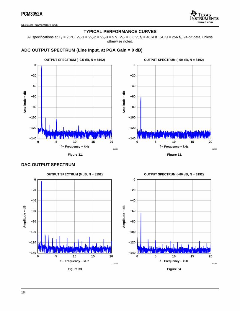
TYPICAL PERFORMANCE CURVES
ADC OUTPUT SPECTRUM (Line Input, at PGA Gain = 0 dB)
f − Frequency − kHz
−140
−120
−100
−80
−60
−40
−20
0
0 5 10 15 20
Am
plit
ud
e −
dB
G031f − Frequency − kHz
−140
−120
−100
−80
−60
−40
−20
0
0 5 10 15 20
Am
plit
ud
e −
dB
G032
DAC OUTPUT SPECTRUM
f − Frequency − kHz
−140
−120
−100
−80
−60
−40
−20
0
0 5 10 15 20
Am
plit
ud
e −
dB
G033f − Frequency − kHz
−140
−120
−100
−80
−60
−40
−20
0
0 5 10 15 20
Am
plit
ud
e −
dB
G034
PCM3052A
SLES160–NOVEMBER 2005
All specifications at TA = 25°C, VCC1 = VCC2 = VCC3 = 5 V, VDD = 3.3 V, fS = 48 kHz, SCKI = 256 fS, 24-bit data, unlessotherwise noted.
OUTPUT SPECTRUM (–0.5 dB, N = 8192) OUTPUT SPECTRUM (–60 dB, N = 8192)
Figure 31. Figure 32.
OUTPUT SPECTRUM (0 dB, N = 8192) OUTPUT SPECTRUM (–60 dB, N = 8192)
Figure 33. Figure 34.
18
www.ti.com
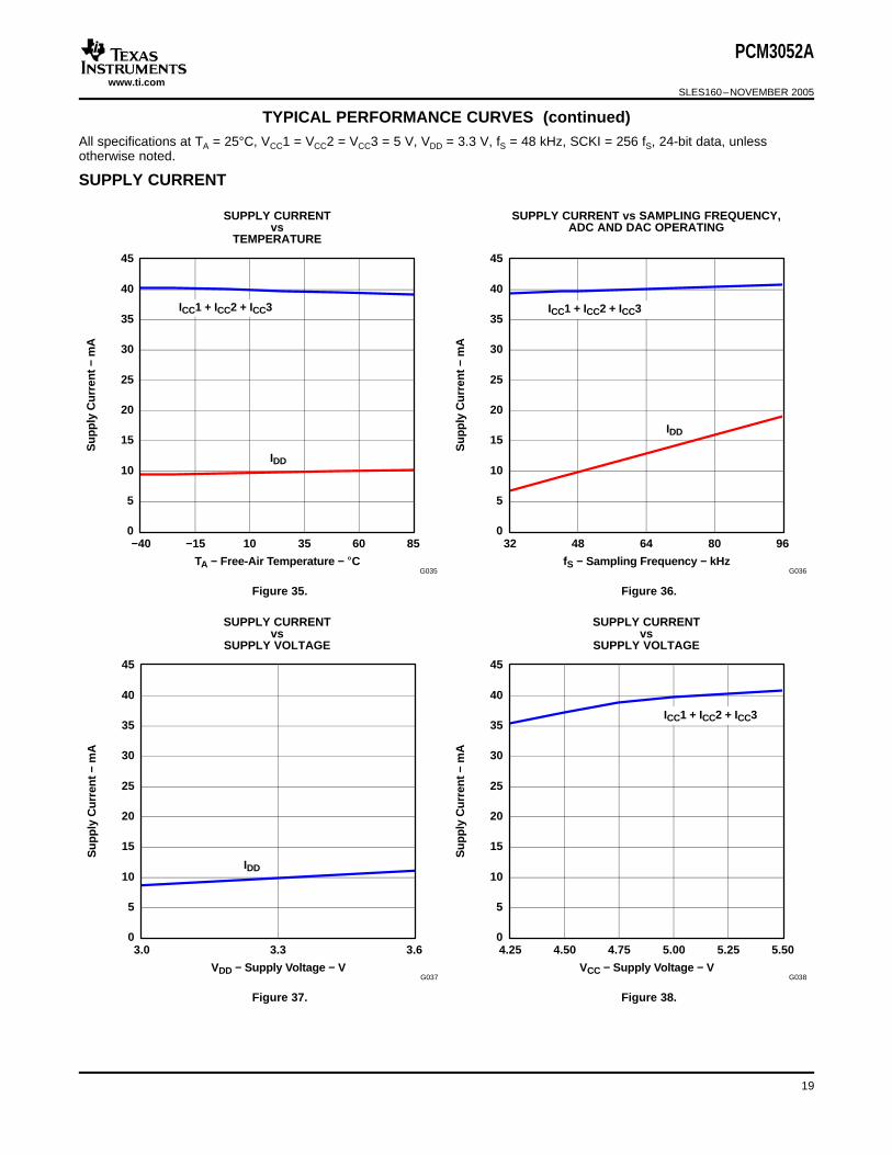
SUPPLY CURRENT
0
5
10
15
20
25
30
35
40
45
−40 −15 10 35 60 85
Su
pp
ly C
urr
ent −
mA
TA − Free-Air Temperature − °CG035
IDD
ICC1 + ICC2 + ICC3
0
5
10
15
20
25
30
35
40
45
32 48 64 80 96
Su
pp
ly C
urr
ent −
mA
fS − Sampling Frequency − kHzG036
IDD
ICC1 + ICC2 + ICC3
0
5
10
15
20
25
30
35
40
45
3.0 3.3 3.6
Su
pp
ly C
urr
ent −
mA
VDD − Supply Voltage − VG037
IDD
0
5
10
15
20
25
30
35
40
45
4.25 4.50 4.75 5.00 5.25 5.50
Su
pp
ly C
urr
ent −
mA
VCC − Supply Voltage − VG038
ICC1 + ICC2 + ICC3
PCM3052A
SLES160–NOVEMBER 2005
TYPICAL PERFORMANCE CURVES (continued)All specifications at TA = 25°C, VCC1 = VCC2 = VCC3 = 5 V, VDD = 3.3 V, fS = 48 kHz, SCKI = 256 fS, 24-bit data, unlessotherwise noted.
SUPPLY CURRENT SUPPLY CURRENT vs SAMPLING FREQUENCY,vs ADC AND DAC OPERATING
TEMPERATURE
Figure 35. Figure 36.
SUPPLY CURRENT SUPPLY CURRENTvs vs
SUPPLY VOLTAGE SUPPLY VOLTAGE
Figure 37. Figure 38.
19
www.ti.com
THEORY OF OPERATION
ADC SECTION
1st
SW-CAPIntegrator
AnalogInX(z) +
−
+− 2nd
SW-CAPIntegrator
3rd
SW-CAPIntegrator
+− 4th
SW-CAPIntegrator
++
++
++
++
5th
SW-CAPIntegrator
DigitalOutY(z)
Comparator
Qn(z)
H(z)
1-BitDAC
STF(z) = H(z) / [1 + H(z)]NTF(z) = 1 / [1 + H(z)]
Y(z) = STF(z) * X(z) + NTF(z) * Qn(z)Signal Transfer FunctionNoise Transfer Function
B0005-02
DAC SECTION
PCM3052A
SLES160–NOVEMBER 2005
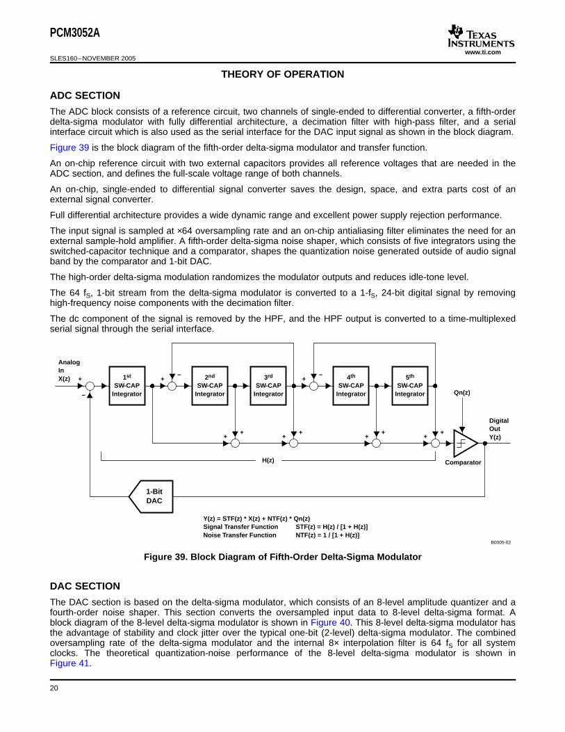
The ADC block consists of a reference circuit, two channels of single-ended to differential converter, a fifth-orderdelta-sigma modulator with fully differential architecture, a decimation filter with high-pass filter, and a serialinterface circuit which is also used as the serial interface for the DAC input signal as shown in the block diagram.
Figure 39 is the block diagram of the fifth-order delta-sigma modulator and transfer function.
An on-chip reference circuit with two external capacitors provides all reference voltages that are needed in theADC section, and defines the full-scale voltage range of both channels.
An on-chip, single-ended to differential signal converter saves the design, space, and extra parts cost of anexternal signal converter.
Full differential architecture provides a wide dynamic range and excellent power supply rejection performance.
The input signal is sampled at ×64 oversampling rate and an on-chip antialiasing filter eliminates the need for anexternal sample-hold amplifier. A fifth-order delta-sigma noise shaper, which consists of five integrators using theswitched-capacitor technique and a comparator, shapes the quantization noise generated outside of audio signalband by the comparator and 1-bit DAC.
The high-order delta-sigma modulation randomizes the modulator outputs and reduces idle-tone level.
The 64 fS, 1-bit stream from the delta-sigma modulator is converted to a 1-fS, 24-bit digital signal by removinghigh-frequency noise components with the decimation filter.
The dc component of the signal is removed by the HPF, and the HPF output is converted to a time-multiplexedserial signal through the serial interface.
Figure 39. Block Diagram of Fifth-Order Delta-Sigma Modulator
The DAC section is based on the delta-sigma modulator, which consists of an 8-level amplitude quantizer and afourth-order noise shaper. This section converts the oversampled input data to 8-level delta-sigma format. Ablock diagram of the 8-level delta-sigma modulator is shown in Figure 40. This 8-level delta-sigma modulator hasthe advantage of stability and clock jitter over the typical one-bit (2-level) delta-sigma modulator. The combinedoversampling rate of the delta-sigma modulator and the internal 8× interpolation filter is 64 fS for all systemclocks. The theoretical quantization-noise performance of the 8-level delta-sigma modulator is shown inFigure 41.
20

www.ti.com
B0008-03
++
−
Z–1
++ +
++
+
8-Level Quantizer
−Z–1
IN8 fS
OUT64 fS
++
Z–1
++
Z–1
+
−180
−160
−140
−120
−100
−80
−60
−40
−20
0
0 1 2 3 4 5 6 7 8
fS − Sampling Frequency − kHzG039
Am
plit
ud
e −
dB
90
95
100
105
110
115
120
125
0 100 200 300 400 500 600
Jitter − psP−PG040
Dyn
amic
Ran
ge
− d
B
PCM3052A
SLES160–NOVEMBER 2005
THEORY OF OPERATION (continued)
Figure 40. 8-Level Delta-Sigma Modulator Block Diagram
Figure 41. Quantization Noise Spectrum Figure 42. Clock Jitter
21
www.ti.com
SYSTEM CLOCK
tw(SCKH)
tw(SCKL)
2 V
0.8 V
1/256 fS
T0005−10
System Clock
POWER SUPPLY ON, EXTERNAL RESET, AND POWER DOWN
PCM3052A
SLES160–NOVEMBER 2005
THEORY OF OPERATION (continued)
The system clock for the PCM3052A must be 256 fS, where fS is the audio sampling rate, 16 kHz to 96 kHz.Table 1 lists typical system clock frequencies, and Figure 43 illustrates the system clock timing.
Table 1. Typical System Clock
SAMPLING RATE SYSTEM CLOCK FREQUENCY – MHzFREQUENCY (fS) – LRCK 256 fS
16 kHz 4.096
32 kHz 8.192
44.1 kHz 11.2896
48 kHz 12.288
96 kHz 24.576
PARAMETER MIN MAX UNIT
tw(SCKH) System clock pulse duration, HIGH 16 ns
tw(SCKL) System clock pulse duration, LOW 16 ns
Figure 43. System Clock Timing
The PCM3052A has both an internal power-on-reset circuit and an external reset circuit. The sequences for bothresets are shown as follows.
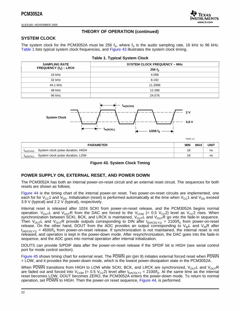
Figure 44 is the timing chart of the internal power-on reset. Two power-on-reset circuits are implemented, oneeach for for VCC1 and VDD. Initialization (reset) is performed automatically at the time when VCC1 and VDD exceed3.9 V (typical) and 2.2 V (typical), respectively.
Internal reset is released after 1024 SCKI from power-on-reset release, and the PCM3052A begins normaloperation. VOUTL and VOUTR from the DAC are forced to the VCOM (= 0.5 VCC2) level as VCC2 rises. Whensynchronization between SCKI, BCK, and LRCK is maintained, VOUTL and VOUTR go into the fade-in sequence.Then VOUTL and VOUTR provide outputs corresponding to DIN after t(DACDLY1) = 2100/fS from power-on-resetrelease. On the other hand, DOUT from the ADC provides an output corresponding to VINL and VINR aftert(ADCDLY1) = 4500/fS from power-on-reset release. If synchronization is not maintained, the internal reset is notreleased, and operation is kept in the power-down mode. After resynchronization, the DAC goes into the fade-insequence, and the ADC goes into normal operation after internal initialization.
DOUTS can provide S/PDIF data after the power-on-reset release if the SPDIF bit is HIGH (see serial controlport for mode control section).
Figure 45 shows timing chart for external reset. The PDWN pin (pin 9) initiates external forced reset when PDWN= LOW, and it provides the power-down mode, which is the lowest power-dissipation state in the PCM3052A.
When PDWN transitions from HIGH to LOW while SCKI, BCK, and LRCK are synchronized, VOUTL and VOUTRare faded out and forced into VCOM (= 0.5 VCC2) level after tDACDLY1 = 2100/fS. At the same time as the internalreset becomes LOW, DOUT becomes ZERO, the PCM3052A enters the power-down mode. To return to normaloperation, set PDWN to HIGH. Then the power-on reset sequence, Figure 44, is performed.
22
www.ti.com
VCC1, VDD 0 V
LRCK, BCK,SCKI
DOUT
1024 SCKI
Internal Reset
Synchronous Clocks
Power Down Normal Operation
ZERO
PDWN
VOUTL, VOUTR
(VCC1 = 5 V,VDD = 3.3 V Typ)
(VCC1 = 3.9 V, VDD = 2.2 V Typ)
DOUTS
t(DACDLY1), 2100 /fS
VCOM (0.5 VCC2)
About 40/fS
t(ADCDLY1), 4500 /fS
Enable if S/PDIF Bit = HIGHDisable
T0097-01
PCM3052A
SLES160–NOVEMBER 2005
DOUTS is driven LOW immediately after PDWN is asserted and recovers about 40/fS following PDWN release.
Notes:1. Large pop noises can be generated on VOUTL and VOUTR if the power supply is turned off during normal
operation.2. To switch PDWN during fade-in or fade-out causes an immediate change between fade-in and fade-out.3. Changing mode controls during normal operation can degrade analog performance. It is recommended that
mode controls be changed through the serial control port, and that changing or stopping the clock, switchingthe power supply off, etc., be done in the power-down mode.
Figure 44. DAC Output and ADC Output for Power-On Reset
23

www.ti.com
VCC1, VCC2,VCC3, VDD
LRCK, BCK,SCKI
DOUT
1024 SCKI
Internal Reset
Synchronous Clocks
Power Down Normal Operation
ZERO
PDWN
VOUTL, VOUTR
(VCC1 − VCC3 = 5 V,VDD = 3.3 V Typ)
DOUTS
t(DACDLY1), 2100 /fS
VCOM (0.5 VCC2)
About 40/fS
T0098-01
0 V
Synchronous Clocks
0.5 VCC2
Normal Operation
t(DACDLY1), 2100 /fS
LOW
t(ADCDLY1), 4500 /fS
PCM3052A
SLES160–NOVEMBER 2005
Figure 45. DAC Output and ADC Output for External Reset (PDWN Pin)
24
www.ti.com
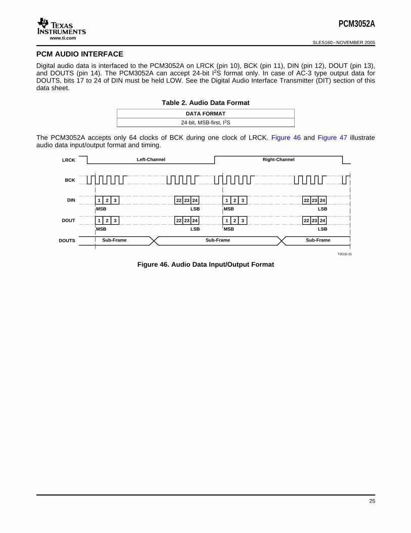
PCM AUDIO INTERFACE
LRCK Right-ChannelLeft-Channel
BCK
DIN
MSB LSB
22 23 24321
T0016-15
MSB LSB
22 23 24321
DOUT
MSB LSB
22 23 24321
MSB LSB
22 23 24321
DOUTS Sub-Frame Sub-Frame Sub-Frame
PCM3052A
SLES160–NOVEMBER 2005
Digital audio data is interfaced to the PCM3052A on LRCK (pin 10), BCK (pin 11), DIN (pin 12), DOUT (pin 13),and DOUTS (pin 14). The PCM3052A can accept 24-bit I2S format only. In case of AC-3 type output data forDOUTS, bits 17 to 24 of DIN must be held LOW. See the Digital Audio Interface Transmitter (DIT) section of thisdata sheet.
Table 2. Audio Data Format
DATA FORMAT
24-bit, MSB-first, I2S
The PCM3052A accepts only 64 clocks of BCK during one clock of LRCK. Figure 46 and Figure 47 illustrateaudio data input/output format and timing.
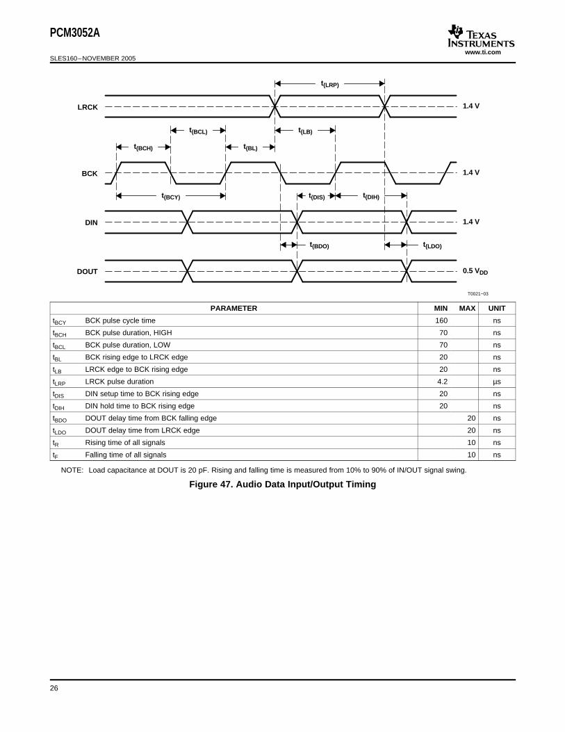
Figure 46. Audio Data Input/Output Format
25
www.ti.com
BCK
LRCK
DIN
t(BCH)
t(BCL)
t(LRP)
t(LB)
t(BCY)
1.4 V
t(BL)
DOUT
t(BDO) t(LDO)
0.5 VDD
t(DIS) t(DIH)
1.4 V
1.4 V
T0021−03
PCM3052A
SLES160–NOVEMBER 2005
PARAMETER MIN MAX UNIT
tBCY BCK pulse cycle time 160 ns
tBCH BCK pulse duration, HIGH 70 ns
tBCL BCK pulse duration, LOW 70 ns
tBL BCK rising edge to LRCK edge 20 ns
tLB LRCK edge to BCK rising edge 20 ns
tLRP LRCK pulse duration 4.2 µs
tDIS DIN setup time to BCK rising edge 20 ns
tDIH DIN hold time to BCK rising edge 20 ns
tBDO DOUT delay time from BCK falling edge 20 ns
tLDO DOUT delay time from LRCK edge 20 ns
tR Rising time of all signals 10 ns
tF Falling time of all signals 10 ns
NOTE: Load capacitance at DOUT is 20 pF. Rising and falling time is measured from 10% to 90% of IN/OUT signal swing.
Figure 47. Audio Data Input/Output Timing
26
www.ti.com
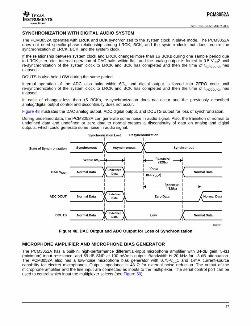
SYNCHRONIZATION WITH DIGITAL AUDIO SYSTEM
Within 6/fSt(DACDLY2)
(32/fS)
Normal DataVCOM
(0.5 VCC2)
UndefinedDataNormal Data
SynchronousAsynchronousSynchronous
ResynchronizationSynchronization Lost
DAC VOUT
State of Synchronization
Normal DataZero DataNormal DataADC DOUT
t(ADCDLY2)(32/fS)
UndefinedData
T0020-07
Normal DataLowNormal DataDOUTSUndefined
Data
MICROPHONE AMPLIFIER AND MICROPHONE BIAS GENERATOR
PCM3052A
SLES160–NOVEMBER 2005
The PCM3052A operates with LRCK and BCK synchronized to the system clock in slave mode. The PCM3052Adoes not need specific phase relationship among LRCK, BCK, and the system clock, but does require thesynchronization of LRCK, BCK, and the system clock.
If the relationship between system clock and LRCK changes more than ±6 BCKs during one sample period dueto LRCK jitter, etc., internal operation of DAC halts within 6/fS, and the analog output is forced to 0.5 VCC2 untilre-synchronization of the system clock to LRCK and BCK has completed and then the time of t(DACDLY2) haselapsed.
DOUTS is also held LOW during the same period.
Internal operation of the ADC also halts within 6/fS, and digital output is forced into ZERO code untilre-synchronization of the system clock to LRCK and BCK has completed and then the time of t(ADCDLY2) haselapsed.
In case of changes less than ±5 BCKs, re-synchronization does not occur and the previously describedanalog/digital output control and discontinuity does not occur.
Figure 48 illustrates the DAC analog output, ADC digital output, and DOUTS output for loss of synchronization.
During undefined data, the PCM3052A can generate some noise in audio signal. Also, the transition of normal toundefined data and undefined or zero data to normal creates a discontinuity of data on analog and digitaloutputs, which could generate some noise in audio signal.
Figure 48. DAC Output and ADC Output for Loss of Synchronization
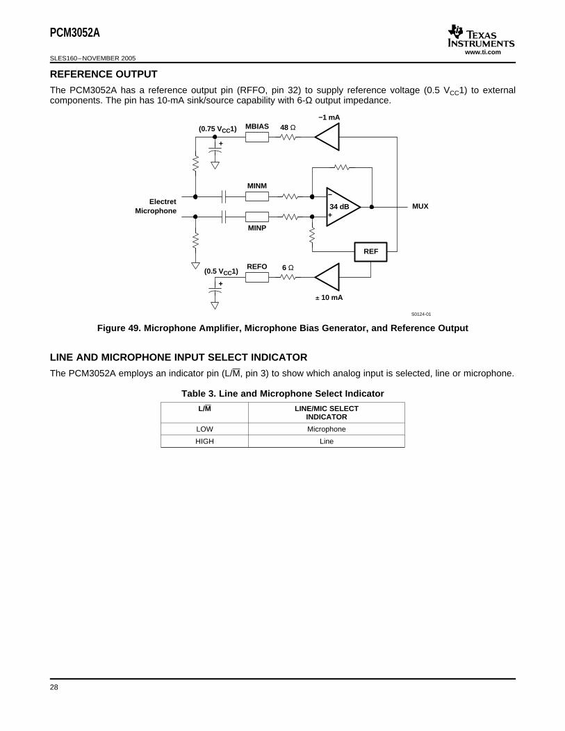
The PCM3052A has a built-in, high-performance differential-input microphone amplifier with 34-dB gain, 5-kΩ(minimum) input resistance, and 59-dB SNR at 100-mVrms output. Bandwidth is 20 kHz for –3-dB attenuation.The PCM3052A also has a low-noise microphone bias generator with 0.75-VCC1 and 1-mA current-sourcecapability for electret microphones. Output impedance is 48 Ω for external noise reduction. The output of themicrophone amplifier and the line input are connected as inputs to the multiplexer. The serial control port can beused to control which input the multiplexer selects (see Figure 50).
27
www.ti.com
REFERENCE OUTPUT
+
−
MUX
S0124-01
ElectretMicrophone
MINM
MINP
REF
34 dB
10 mA
6 ΩREFO
+
(0.5 VCC1)
−1 mA48 ΩMBIAS
+
(0.75 VCC1)
LINE AND MICROPHONE INPUT SELECT INDICATOR
PCM3052A
SLES160–NOVEMBER 2005
The PCM3052A has a reference output pin (RFFO, pin 32) to supply reference voltage (0.5 VCC1) to externalcomponents. The pin has 10-mA sink/source capability with 6-Ω output impedance.
Figure 49. Microphone Amplifier, Microphone Bias Generator, and Reference Output
The PCM3052A employs an indicator pin (L/M, pin 3) to show which analog input is selected, line or microphone.
Table 3. Line and Microphone Select Indicator
L/M LINE/MIC SELECTINDICATOR
LOW Microphone
HIGH Line
28

www.ti.com
MULTIPLEXER AND PGA
RIN(k, typical) 2861 10(PGA Gain20) (1)
LIN+
S0125-01
VINL L-ch−1
PGA (−4 dB to 20 dB)R
R
LIN−
2-ch MUX
RIN+VINR R-ch
−1
PGA (−4 dB to 20 dB)R
R
RIN−
Mic Amp
ANALOG OUTPUTS FROM DAC
VCOM OUTPUT FOR DAC
DIGITAL AUDIO INTERFACE TRANSMITTER (DIT)
PCM3052A
SLES160–NOVEMBER 2005
The PCM3052A has built-in analog front-end circuit which is shown in Figure 50. Multiplexer input and PGA gainare selected by mode control via the serial port, as shown in the Serial Control Port for Mode Control section.The full-scale input voltage range is 0.1 Vrms to 1.5 Vrms, and it can be adjusted to an adequate level forfollowing the ADC sections.
VINL and VINR input resistance is maintained above 22 kΩ for all PGA gains. The input resistance value for eachgain can be calculated by Equation 1.
Figure 50. Multiplexer and PGA
The PCM3052A has two independent output channels, VOUTL and VOUTR. These are unbalanced outputs, eachcapable of driving 4 Vp-p (typical) into a 5-kΩ ac-coupled load. The internal output amplifiers for VOUTL andVOUTR are biased to the dc common-mode (or bipolar zero) voltage, equal to 0.5 VCC2
The output amplifiers include an RC continuous-time filter, which helps to reduce the out-of-band noise energypresent at the DAC outputs due to the noise-shaping characteristics of the PCM3052A delta-sigma modulators.The frequency response of this filter is shown in the typical performance curves. By itself, this filter is notadequate to attenuate the out-of-band noise to an acceptable level for many applications. An external low-passfilter is required to provide sufficient out-of-band noise rejection. Further discussion of DAC post-filter circuits isprovided in the PCM1742 data sheet (SBAS176).
One unbuffered common-mode voltage output pin, VCOM (pin 26), is brought out for decoupling purposes. Thispin is nominally biased to a dc voltage level equal to 0.5 VCC2. This pin can be used to bias external circuits.Output resistance of this pin is 21 kΩ (typical).
The PCM3052A employs S/PDIF output from DOUTS (pin 14). The data (I2S format only) from DAC digital datainput (DIN, pin 12) is encoded to S/PDIF format with preambles according to IEC958. S/PDIF output is controlledthrough the serial control port. The output data type (linear PCM or AC-3) can be also selected through the serialcontrol port. For the output data type of AC-3, the word length is limited to 16 bits in the PCM3052A. Therefore,bits 17 to 24 in the I2S format data must be set to LOW.
29
www.ti.com
T0099-01
SW
DIN(I2S Format)
AC PPaUV
R-chL-ch
Frame
R-ch
Frame
SWAP
L-ch
Frame
R-ch
Enable
LOW
Disable
L-ch
Frame
S/PDIF OutputControl Bit
DOUTS
P: PreambleA: Aux
U: User BitsC: Channel Status
SW: Audio Sample WordV: Validity Bit
Pa: Parity Bit
AC PPaUV
32/fS Frame
PCM3052A
SLES160–NOVEMBER 2005
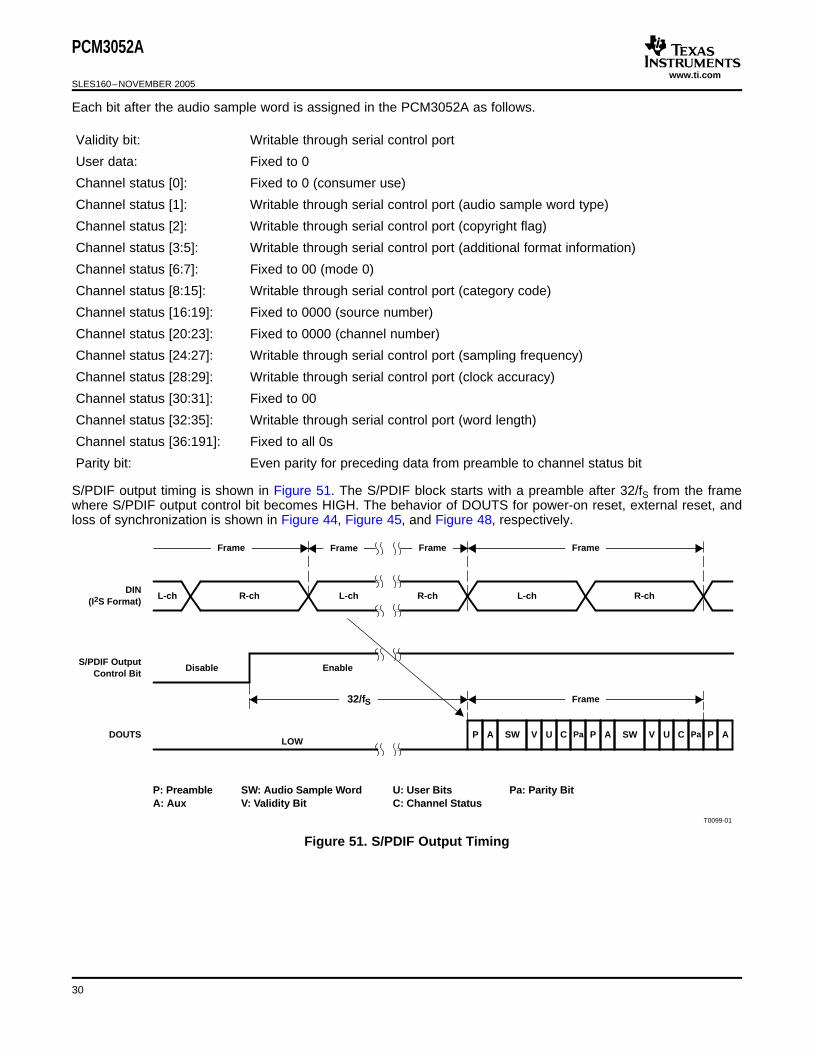
Each bit after the audio sample word is assigned in the PCM3052A as follows.
Validity bit: Writable through serial control port
User data: Fixed to 0
Channel status [0]: Fixed to 0 (consumer use)
Channel status [1]: Writable through serial control port (audio sample word type)
Channel status [2]: Writable through serial control port (copyright flag)
Channel status [3:5]: Writable through serial control port (additional format information)
Channel status [6:7]: Fixed to 00 (mode 0)
Channel status [8:15]: Writable through serial control port (category code)
Channel status [16:19]: Fixed to 0000 (source number)
Channel status [20:23]: Fixed to 0000 (channel number)
Channel status [24:27]: Writable through serial control port (sampling frequency)
Channel status [28:29]: Writable through serial control port (clock accuracy)
Channel status [30:31]: Fixed to 00
Channel status [32:35]: Writable through serial control port (word length)
Channel status [36:191]: Fixed to all 0s
Parity bit: Even parity for preceding data from preamble to channel status bit
S/PDIF output timing is shown in Figure 51. The S/PDIF block starts with a preamble after 32/fS from the framewhere S/PDIF output control bit becomes HIGH. The behavior of DOUTS for power-on reset, external reset, andloss of synchronization is shown in Figure 44, Figure 45, and Figure 48, respectively.
Figure 51. S/PDIF Output Timing
30
www.ti.com
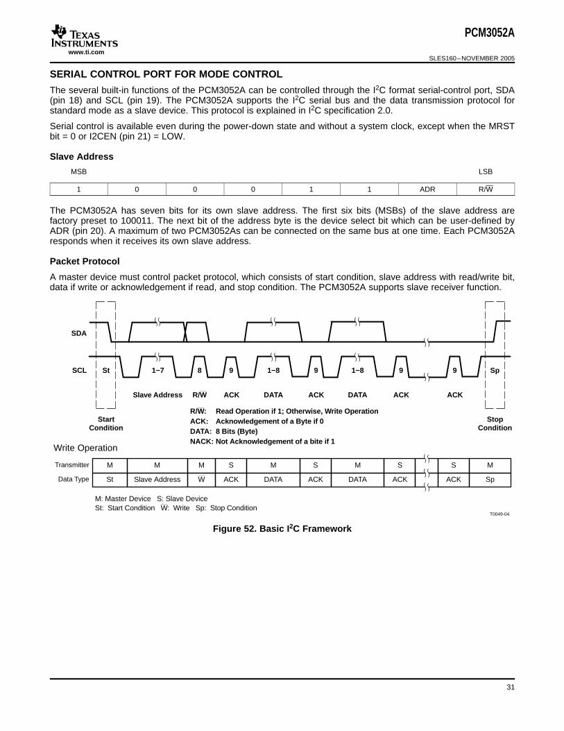
SERIAL CONTROL PORT FOR MODE CONTROL
Slave Address
Packet Protocol
9
SDA
SCL St
Start
1−7 8 1−8 9 1−8 9 9 Sp
Stop
Slave Address ACK DATA ACK DATA ACK ACK
ConditionCondition
R/W
Write Operation
Transmitter M M M S M S M S S M
Data Type St Slave Address W ACK DATA ACK DATA ACK ACK Sp
R/W: Read Operation if 1; Otherwise, Write OperationACK: Acknowledgement of a Byte if 0DATA: 8 Bits (Byte)NACK: Not Acknowledgement of a bite if 1
T0049-04
M: Master Device S: Slave DeviceSt: Start Condition W: Write Sp: Stop Condition
PCM3052A
SLES160–NOVEMBER 2005
The several built-in functions of the PCM3052A can be controlled through the I2C format serial-control port, SDA(pin 18) and SCL (pin 19). The PCM3052A supports the I2C serial bus and the data transmission protocol forstandard mode as a slave device. This protocol is explained in I2C specification 2.0.
Serial control is available even during the power-down state and without a system clock, except when the MRSTbit = 0 or I2CEN (pin 21) = LOW.
MSB LSB
1 0 0 0 1 1 ADR R/W
The PCM3052A has seven bits for its own slave address. The first six bits (MSBs) of the slave address arefactory preset to 100011. The next bit of the address byte is the device select bit which can be user-defined byADR (pin 20). A maximum of two PCM3052As can be connected on the same bus at one time. Each PCM3052Aresponds when it receives its own slave address.
A master device must control packet protocol, which consists of start condition, slave address with read/write bit,data if write or acknowledgement if read, and stop condition. The PCM3052A supports slave receiver function.
Figure 52. Basic I2C Framework
31

www.ti.com
Write Operation
R0002-03
M: Master Device S: Slave DeviceSt: Start Condition ACK: Acknowledge W: Write Sp: Stop Condition
Transmitter M M M S
Data Type St Slave Address W ACK
M
Reg Address
M
Write Data 1
S
ACK
S
ACK
M
Sp
M
Write Data 2
S
ACK
S
ACK
Serial Control Enable/Disable
T0100-01
0 µs (min)
1 µs (min)
Don’t Care
EnableDisableI2CEN
SDA/SCL HIGH Fixed
Don’t CareADR HIGH or LOW
PCM3052A
SLES160–NOVEMBER 2005
The PCM3052A supports receiver function. A master can write to any PCM3052A registers using single ormultiple accesses. The master sends a PCM3052A slave address with a write bit, a register address, and thedata. If multiple access is required, the address is that of the starting register, followed by the data to betransferred. When the data are received properly, the index register is incremented by 1 automatically. When theindex register reaches 50h, the next value is 41h. When undefined registers are accessed, the PCM3052A doesnot send an acknowledgement. Figure 53 is a diagram of the write operation. The register address and the writedata are 8 bits and MSB-first format.
Figure 53. Framework for Write Operation
The PCM3052A supports I2C serial control enable/disable function by I2CEN (pin 21) to avoid an unstable startcondition. When the I2CEN pin transitions from LOW to HIGH, both SDA (pin 18) and SCL (pin 19) must beHIGH stable and the ADR (pin 20) must be also stable.
While I2CEN = LOW, the write operation is disabled. A timing chart of I2CEN is shown in Figure 54.
Figure 54. I2CEN Timing Chart
32
www.ti.com
TIMING DIAGRAM
SDA
SCL
t(BUF) t(D-SU)
t(D-HD)
Start
t(LOW)
t(S-HD)
t(SCL-F)
t(SCL-R)
t(HI)
Repeated Start
t(RS-SU)
t(RS-HD)
t(SDA-F)
t(SDA-R) t(P-SU)
Stop
T0050-01
MODE CONTROL REGISTERS
User-Programmable Mode Controls
PCM3052A
SLES160–NOVEMBER 2005
PARAMETER CONDITIONS MIN MAX UNIT
f(SCL) SCL clock frequency Standard mode 100 kHz
t(BUF) Bus free time between STOP and START condition Standard mode 4.7 µs
t(LOW) Low period of the SCL clock Standard mode 4.7 µs
t(HI) High period of the SCL clock Standard mode 4 µs
tRS-SU Setup time for START/repeated START condition Standard mode 4.7 µs
t(S-HD) Hold time for START/repeated START condition Standard mode 4 µst(RS-HD)
t(D-SU) Data setup time Standard mode 250 ns
t(D-HD) Data hold time Standard mode 0 900 ns
t(SCL-R) Rise time of SCL signal Standard mode 20 + 0.1 CB 1000 ns
t(SCL-R1) Rise time of SCL signal after a repeated START condition and after Standard mode 20 + 0.1 CB 1000 nsan acknowledge bit
t(SCL-F) Fall time of SCL signal Standard mode 20 + 0.1 CB 1000 ns
t(SDA-R) Rise time of SDA signal Standard mode 20 + 0.1 CB 1000 ns
t(SDA-F) Fall time of SDA signal Standard mode 20 + 0.1 CB 1000 ns
t(P-SU) Setup time for STOP condition Standard mode 4 µs
CB Capacitive load for SDA and SCL line 400 pF
VNH Noise margin at high level for each connected device (including Standard mode 0.2 VDD Vhysteresis)
Figure 55. Control Interface Timing
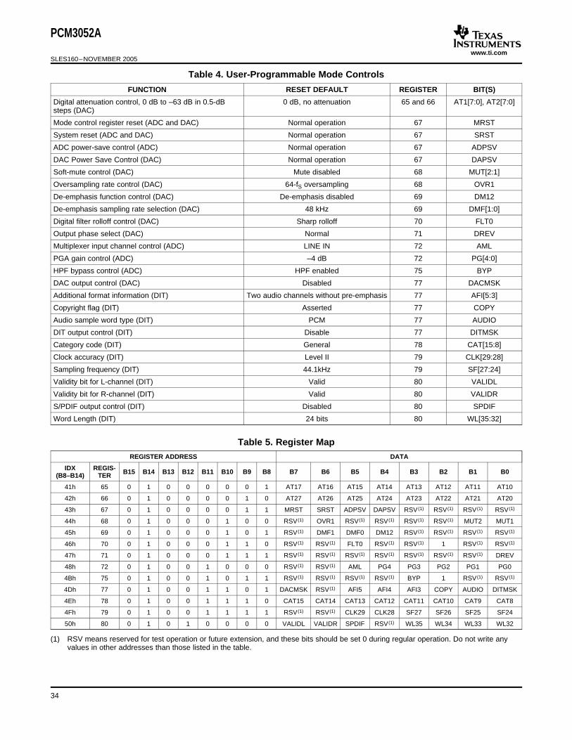
The PCM3052A has several user programmable functions which are accessed via control registers. Theregisters are programmed using the I2C serial control port, which was previously discussed in this data sheet.Table 4 lists the available mode control functions, along with their reset default conditions and associated registeraddresses. The register map is shown in Table 5.
33
www.ti.com
PCM3052A
SLES160–NOVEMBER 2005
Table 4. User-Programmable Mode Controls
FUNCTION RESET DEFAULT REGISTER BIT(S)
Digital attenuation control, 0 dB to –63 dB in 0.5-dB 0 dB, no attenuation 65 and 66 AT1[7:0], AT2[7:0]steps (DAC)
Mode control register reset (ADC and DAC) Normal operation 67 MRST
System reset (ADC and DAC) Normal operation 67 SRST
ADC power-save control (ADC) Normal operation 67 ADPSV
DAC Power Save Control (DAC) Normal operation 67 DAPSV
Soft-mute control (DAC) Mute disabled 68 MUT[2:1]
Oversampling rate control (DAC) 64-fS oversampling 68 OVR1
De-emphasis function control (DAC) De-emphasis disabled 69 DM12
De-emphasis sampling rate selection (DAC) 48 kHz 69 DMF[1:0]
Digital filter rolloff control (DAC) Sharp rolloff 70 FLT0
Output phase select (DAC) Normal 71 DREV
Multiplexer input channel control (ADC) LINE IN 72 AML
PGA gain control (ADC) –4 dB 72 PG[4:0]
HPF bypass control (ADC) HPF enabled 75 BYP
DAC output control (DAC) Disabled 77 DACMSK
Additional format information (DIT) Two audio channels without pre-emphasis 77 AFI[5:3]
Copyright flag (DIT) Asserted 77 COPY
Audio sample word type (DIT) PCM 77 AUDIO
DIT output control (DIT) Disable 77 DITMSK
Category code (DIT) General 78 CAT[15:8]
Clock accuracy (DIT) Level II 79 CLK[29:28]
Sampling frequency (DIT) 44.1kHz 79 SF[27:24]
Validity bit for L-channel (DIT) Valid 80 VALIDL
Validity bit for R-channel (DIT) Valid 80 VALIDR
S/PDIF output control (DIT) Disabled 80 SPDIF
Word Length (DIT) 24 bits 80 WL[35:32]
Table 5. Register MapREGISTER ADDRESS DATA
IDX REGIS- B15 B14 B13 B12 B11 B10 B9 B8 B7 B6 B5 B4 B3 B2 B1 B0(B8–B14) TER
41h 65 0 1 0 0 0 0 0 1 AT17 AT16 AT15 AT14 AT13 AT12 AT11 AT10
42h 66 0 1 0 0 0 0 1 0 AT27 AT26 AT25 AT24 AT23 AT22 AT21 AT20
43h 67 0 1 0 0 0 0 1 1 MRST SRST ADPSV DAPSV RSV (1) RSV (1) RSV (1) RSV (1)
44h 68 0 1 0 0 0 1 0 0 RSV (1) OVR1 RSV (1) RSV (1) RSV (1) RSV (1) MUT2 MUT1
45h 69 0 1 0 0 0 1 0 1 RSV (1) DMF1 DMF0 DM12 RSV (1) RSV (1) RSV (1) RSV (1)
46h 70 0 1 0 0 0 1 1 0 RSV (1) RSV (1) FLT0 RSV (1) RSV (1) 1 RSV (1) RSV (1)
47h 71 0 1 0 0 0 1 1 1 RSV (1) RSV (1) RSV (1) RSV (1) RSV (1) RSV (1) RSV (1) DREV
48h 72 0 1 0 0 1 0 0 0 RSV (1) RSV (1) AML PG4 PG3 PG2 PG1 PG0
4Bh 75 0 1 0 0 1 0 1 1 RSV (1) RSV (1) RSV (1) RSV (1) BYP 1 RSV (1) RSV (1)
4Dh 77 0 1 0 0 1 1 0 1 DACMSK RSV (1) AFI5 AFI4 AFI3 COPY AUDIO DITMSK
4Eh 78 0 1 0 0 1 1 1 0 CAT15 CAT14 CAT13 CAT12 CAT11 CAT10 CAT9 CAT8
4Fh 79 0 1 0 0 1 1 1 1 RSV (1) RSV (1) CLK29 CLK28 SF27 SF26 SF25 SF24
50h 80 0 1 0 1 0 0 0 0 VALIDL VALIDR SPDIF RSV (1) WL35 WL34 WL33 WL32
(1) RSV means reserved for test operation or future extension, and these bits should be set 0 during regular operation. Do not write anyvalues in other addresses than those listed in the table.
34
www.ti.com
REGISTER DEFINITIONS
ATx[7:0]: Digital Attenuation Level Setting (DAC)
MRST: Mode Control Register Reset (ADC and DAC)
SRST: System Reset (ADC and DAC)
PCM3052A
SLES160–NOVEMBER 2005
B15 B14 B13 B12 B11 B10 B9 B8 B7 B6 B5 B4 B3 B2 B1 B0
REGISTER 65 0 1 0 0 0 0 0 1 AT17 AT16 AT15 AT14 AT13 AT12 AT11 AT10
REGISTER 66 0 1 0 0 0 0 1 0 AT27 AT26 AT25 AT24 AT23 AT22 AT21 AT20
Where x = 1 or 2, corresponding to the DAC output VOUTL (x = 1) and VOUTR (x = 2).
Default value: 1111 1111b
ATX[7:0] DECIMAL VALUE ATTENUATION LEVEL SETTING
1111 1111b 255 0 dB, No Attenuation. (default)
1111 1110b 254 –0.5 dB
1111 1101b 253 –1.0 dB
: : :
1000 0011b 131 –62.0 dB
1000 0010b 130 –62.5 dB
1000 0001b 129 –63.0 dB
1000 0000b 128 Mute
: : :
0000 0000b 0 Mute
Each DAC channel (VOUTL and VOUTR) includes a digital attenuation function. The attenuation level can be setfrom 0 dB to –63 dB in 0.5-dB steps, and also can be set to infinite attenuation (mute). The attenuation levelchange from current value to target value is performed by incrementing or decrementing by one small step sizefor every 1/fS time interval during 2048/fS. The small step size is determined automatically so that it can provide atransition in attenuation level with a characteristic S-shaped curve from the current value to the target value.While the attenuation level change sequence is in progress for 2048/fS, processing of the attenuation levelchange for any new command is ignored, and the new command is overwritten into command buffer. The lastcommand for an attenuation level change is performed after present attenuation level change sequence isfinished.
The attenuation data for each channel can be set individually. The attenuation level can be calculated using thefollowing formula:
Attenuation level (dB) = 0.5 × (ATx[7:0]DEC – 255)
where ATx[7:0]DEC = 0 through 255.
For ATx[7:0]DEC = 0 through 128, attenuation is set to infinite attenuation.
The preceding table shows attenuation levels for various settings.
B15 B14 B13 B12 B11 B10 B9 B8 B7 B6 B5 B4 B3 B2 B1 B0
REGISTER 67 0 1 0 0 0 0 1 1 MRST SRST ADPSV DAPSV RSV RSV RSV RSV
Default value: 1
MRST = 0 Set default value
MRST = 1 Normal operation (default)
The MRST bit controls mode control register reset. Pop-noise may be generated.
Default value: 1
35
www.ti.com
ADPSV: ADC Power-Save Control (ADC)
DAPSV: DAC Power-Save Control (DAC)
OVR1: Oversampling Rate Control (DAC)
MUTx: Soft-Mute Control (DAC)
PCM3052A
SLES160–NOVEMBER 2005
SRST = 0 Re-synchronization
SRST = 1 Normal operation (default)
The SRST bit controls system reset. The PCM3052A does not go into power-down state. The mode controlregister is not reset by this control. Also pop-noise may be generated.
Default value: 0
ADPSV = 0 Normal operation (default)
ADPSV = 1 Power-save mode
The ADPSV bit controls ADC power-save mode. In power-save mode, ADC goes into power-down state, thedata in ADC are reset, and DOUT is forced into ZERO immediately. I2C control is enabled.
Default value: 0
DAPSV = 0 Normal operation (default)
DAPSV = 1 Power-save mode
The DAPSV bit controls the DAC power-save mode. In the power-save mode, the DAC output is faded out andDAC goes into the power-down state. I2C control is enabled. A waiting time of more than 2100/fS frompower-save-mode assertion is required for the release of the power-save mode.
DIT function is available if SPDIF bit = 1, even though DAPSV = 1.
B15 B14 B13 B12 B11 B10 B9 B8 B7 B6 B5 B4 B3 B2 B1 B0
REGISTER 68 0 1 0 0 0 1 0 0 RSV OVR1 RSV RSV RSV RSV MUT2 MUT1
Default value: 0
OVR1 = 0 64× oversampling (default)
OVR1 = 1 128× oversampling
The OVR1 bit is used to control the oversampling rate of the delta-sigma D/A converters. To write over thisregister during normal operation may generate noise.
where, x = 1 or 2, corresponding to the DAC output VOUTL (x = 1) and VOUTR (x = 2).
Default value: 0
MUTx = 0 Mute disabled (default)
MUTx = 1 Mute enabled
The mute bits, MUT1 and MUT2, are used to enable or disable the soft-mute function for the corresponding DACoutputs, VOUTL and VOUTR. The soft-mute function is incorporated into the digital attenuators. When mute isdisabled (MUTx = 0), the attenuator and DAC operate normally. When mute is enabled by setting MUTx = 1, thedigital attenuator for the corresponding output is decreased from the current setting to infinite attenuation, oneattenuator step (0.5 dB) for every 8/fS seconds. This provides pop-free muting of the DAC output.
By setting MUTx = 0, the attenuator is increased one step for every 8/fS seconds to the previously programmedattenuation level.
36
www.ti.com
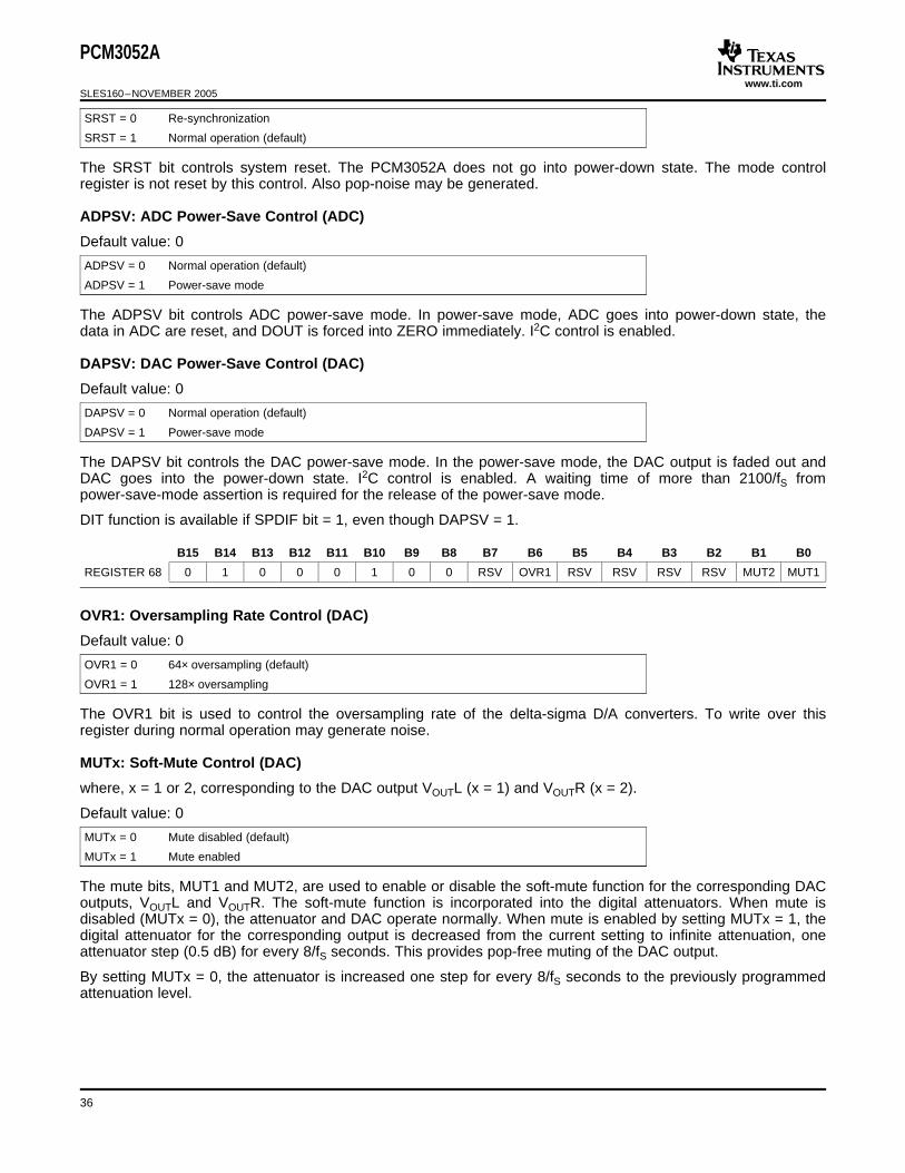
DMF[1:0]: Sampling Frequency Selection for the De-Emphasis Function (DAC)
DM12: Digital De-Emphasis Function Control (DAC)
FLT0: Digital Filter Rolloff Control (DAC)
DREV: Output Phase Select (DAC)
PCM3052A
SLES160–NOVEMBER 2005
B15 B14 B13 B12 B11 B10 B9 B8 B7 B6 B5 B4 B3 B2 B1 B0
REGISTER 69 0 1 0 0 0 1 0 1 RSV DMF1 DMF0 DM12 RSV RSV RSV RSV
Default value: 01
DMF[1:0] DE-EMPHASIS SAMPLING RATE SELECTION
0 0 44.1 kHz
0 1 48 kHz (default)
1 0 32 kHz
1 1 Reserved
The DMF[1:0] bits are used to select the sampling frequency used for the digital de-emphasis function when it isenabled.
Default value: 0
DM12 = 0 De-emphasis disabled (default)
DM12 = 1 De-emphasis enabled
The DM12 bit is used to enable or disable the digital de-emphasis function. See the plots shown in the TypicalPerformance Curves section of this data sheet.
B15 B14 B13 B12 B11 B10 B9 B8 B7 B6 B5 B4 B3 B2 B1 B0
REGISTER 70 0 1 0 0 0 1 1 0 RSV RSV FLT0 RSV RSV 1 RSV RSV
Default value: 0
FLT0 = 0 Sharp rolloff (default)
FLT0 = 1 Slow rolloff
The FLT0 bit allows the user to select the digital filter rolloff that is best suited to their application. Two filter rolloffselections are available: Sharp and Slow. The filter responses for these selections are shown in the TypicalPerformance Curves section of this data sheet.
B15 B14 B13 B12 B11 B10 B9 B8 B7 B6 B5 B4 B3 B2 B1 B0
REGISTER 71 0 1 0 0 0 1 1 1 RSV RSV RSV RSV RSV RSV RSV DREV
Default value: 0
DREV = 0 Normal output (default)
DREV = 1 Inverted output
The DREV bit is used to control the output analog signal phase control.
37

www.ti.com
AML: Multiplexer Input Channel Selection (ADC)
PG[4:0]: PGA Gain Selection (ADC)
BYP: HPF Bypass Control (ADC)
PCM3052A
SLES160–NOVEMBER 2005
B15 B14 B13 B12 B11 B10 B9 B8 B7 B6 B5 B4 B3 B2 B1 B0
REGISTER 72 0 1 0 0 1 0 0 0 RSV RSV AML PG4 PG3 PG2 PG1 PG0
Default value: 0
AML MULTIPLEXER INPUT CHANNEL SELECTION
0 Line (default)
1 Microphone
The AML bit selects the input channel of multiplexer.
Default value: 0 0100 (–4 dB)
PG[4:0] PGA Gain Selection PG[4:0] PGA Gain Selection
11111 Digital mute 01111 7 dB
11110 Digital mute 01110 6 dB
11101 Digital mute 01101 5 dB
11100 20 dB 01100 4 dB
11011 19 dB 01011 3 dB
11010 18 dB 01010 2 dB
11001 17 dB 01001 1 dB
11000 16 dB 01000 0 dB
10111 15 dB 00111 – 1 dB
10110 14 dB 00110 –2 dB
10101 13 dB 00101 –3 dB
10100 12 dB 00100 –4 dB (default)
10011 11 dB 00011 Digital mute
10010 10 dB 00010 Digital mute
10001 9 dB 00001 Digital mute
10000 8 dB 00000 Digital mute
The PG[4:0] bits control the gain of PGA for adjusting the signal level for ADC.
B15 B14 B13 B12 B11 B10 B9 B8 B7 B6 B5 B4 B3 B2 B1 B0
REGISTER 75 0 1 0 0 1 0 1 1 RSV RSV RSV RSV BYP 1 RSV RSV
Default value: 0
BYP = 0 Normal output, HPF enable (default)
BYP = 1 Bypass output, HPF disable
The BYP bit controls HPF function; dc components of input and dc offset are converted in bypass mode.
38

www.ti.com
DACMSK: DAC Output Control (DAC)
AFI[5:3]: Additional Format Information (DIT)
COPY: Copyright Flag (DIT)
AUDIO: Audio Sample Word Type (DIT)
DITMSK: DIT Output Control (DIT)
PCM3052A
SLES160–NOVEMBER 2005
B15 B14 B13 B12 B11 B10 B9 B8 B7 B6 B5 B4 B3 B2 B1 B0
REGISTER 77 0 1 0 0 1 1 0 1 DACMSK RSV AFI5 AFI4 AFI3 COPY AUDIO DITMSK
Default value: 0
DACMSK = 0 Mask disable (default)
DACMSK = 1 Mask DIN to BPZ level
The DACMSK bit is used to mask DIN to BPZ level. The analog outputs from DAC is forced to BPZ levelimmediately. Larger noise may be generated by this control.
Default value: 000 (2 audio channels without pre-emphasis)
The AFI[5:3] bits control bits[5:3] of channel status bits in compliance with IEC958.
Default value: 0 (Asserted)
The COPY bit controls bit[2] of channel status bits in compliance with IEC958.
Default value: 0 (PCM)
The AUDIO bit controls bit[1] of channel status bits in compliance with IEC958.
Default value: 0
DITMSK = 0 Mask disable (default)
DITMSK = 1 Force DOUTS to encoded ZERO status
The DITMSK bit forces only aux and audio sample words on DOUTS to encoded ZERO status. As for validityand channel status bits, the values in the register are output.
39

www.ti.com
CAT[15:8]: Category Code (DIT)
CLK[29:28]: Clock Accuracy (DIT)
SF[27:24]: Sampling Frequency (DIT)
VALIDL: Validity Bit for L-channel (DIT)
VALIDR: Validity Bit for R-channel (DIT)
SPDIF: S/PDIF Output Control (DIT)
WL[35:32]: Word Length (DIT)
PCM3052A
SLES160–NOVEMBER 2005
B15 B14 B13 B12 B11 B10 B9 B8 B7 B6 B5 B4 B3 B2 B1 B0
REGISTER 78 0 1 0 0 1 1 1 0 CAT15 CAT14 CAT13 CAT12 CAT11 CAT10 CAT9 CAT8
Default value: 0000 0000 (general)
The CAT[15:8] bits control bits[15:8] of channel status bits in compliance with IEC958.
B15 B14 B13 B12 B11 B10 B9 B8 B7 B6 B5 B4 B3 B2 B1 B0
REGISTER 79 0 1 0 0 1 1 1 1 RSV RSV CLK29 CLK28 SF27 SF26 SF25 SF24
Default value: 00 (level II)
The CLK[29:28] bits control bits[29:28] of channel status bits in compliance with IEC958.
Default value: 0000 (44.1 kHz)
The SF[27:24] bits control bits[27:24] of channel status bits in compliance with IEC958.
B15 B14 B13 B12 B11 B10 B9 B8 • B7 B6 B5 B4 B3 B2 B1 B0
REGISTER 80 0 1 0 1 0 0 0 0 VALIDL VALIDR SPDIF RSV WL35 WL34 WL33 WL32
Default value: 0 (valid)
The VALIDL bit controls the validity bit for L-channel in compliance with IEC958.
Default value: 0 (valid)
The VALIDR bit controls validity bit for R-channel in compliance with IEC958.
Default value: 0
SPDIF = 0 DOUTS disabled (default)
SPDIF = 1 DOUTS enabled
The SPDIF bit controls output from DOUTS pin. In case of default, DOUTS always becomes LOW status.
Default value: 0001 (24 bits)
The WL[35:32] bits control bits[35:32] of channel status bits and the actual data word length of audio sampleword including auxiliary 4-bits from DOUTS pin in compliance with IEC958. If the WL[35:32] bits indicate 16 bits,the actual data word length of audio sample word is limited to 16 bits even though data input on DIN pin is24-bits, for example.
40
www.ti.com
TYPICAL CIRCUIT CONNECTION
VCOM
MBIAS
MINM
MINP
AGND3
VCC3
REFO
VDD
DGND
DOUTS
DOUT
DIN
BCK
LRCK
PCM3052A
26
27
28
29
30
31
32
16
15
14
13
12
11
10
AT
ES
T
VIN
L
L/M
VR
EF1
VR
EF2
VIN
R
VC
C1
AG
ND
1
PD
WN
1 2 3 4 5 6 7 8 9
VO
UTL
VO
UTR
VC
C2
AG
ND
2
I2C
EN
AD
R
SC
L
SD
A
SC
KI
25 24 23 22 21 20 19 18 17
PostLPF
+
+ C13
+ C14
+ C2
Line Out Control
5 VGND
+
C9
C10
C8+
C3
C7
+C15 R1
R2
+
Mic In
3.3 V
+
C4
System ClockandAudio Interface
C1
+C12
+C6
+C5
+C11
Line InS0126-01
PCM3052A
SLES160–NOVEMBER 2005
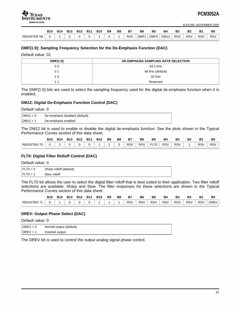
Figure 56 illustrates typical circuit connection.
NOTE: C1– C4: 0.1-µF ceramic and 10-µF electrolytic capacitors typical, depending on power supply quality and patternlayout.C5– C8: 0.1-µF ceramic and 10-µF electrolytic capacitors are recommended.C9, C10: 1-µF non-polar electrolytic capacitors are recommended, which give 27-Hz cutoff frequency.C11, C12: 0.22-µF electrolytic capacitors are recommended, which give 5-Hz cutoff frequency at PGA gain = 0 dB.C13, C14: 2.2-µF electrolytic capacitors are typical.C15: 10-µF electrolytic capacitor is recommended.R1, R2: 1-kΩ typical is recommended.
Figure 56. Typical Application Diagram
41
www.ti.com
DESIGN AND LAYOUT CONSIDERATIONS IN APPLICATION
Power Supply Pins (VCC1, VCC2, VCC3, VDD)
Grounding (AGND1, AGND2, AGND3, DGND)
VINL, VINR Pins
VREF1, VREF2, VCOM Pins
MBIAS Pin
REFO Pin
MINM, MINP Pins
System Clock
External Mute Control
PCM3052A
SLES160–NOVEMBER 2005
The digital and analog power supply lines to the PCM3052A should be bypassed to the corresponding groundpins with 0.1-µF ceramic and 10-µF electrolytic capacitors as close to the pins as possible to maximize thedynamic performance of the ADC and DAC.
Although the PCM3052A has four power lines to maximize the potential of dynamic performance, using onecommon 5-V power supply for VCC1, VCC2, and VCC3. A 3.3-V power supply for VDD, which is generated from the5-V power supply for VCC1, VCC2, and VCC3, is recommended to avoid unexpected power supply trouble likelatch-up or power supply sequencing problems.
To maximize the dynamic performance of the PCM3052A, the analog and digital grounds are not connectedinternally. These points should have low impedance to avoid digital noise and signal components feeding backinto the analog ground. They should be connected directly to each other under the parts to reduce the potentialof noise problems.
A 0.22-µF electrolytic capacitor is recommended as an ac-coupling capacitor, which gives a 5-Hz cutofffrequency at PGA gain = 0 dB. If higher full-scale input voltage is required, it can be adjusted by adding only oneseries resistor to VINX pins.
Both 0.1-µF ceramic and 10-µF electrolytic capacitors are recommended from VREF1 and VREF2 to AGND1, andfrom VCOM to AGND2, to ensure low source impedance of the ADC and DAC references. These capacitorsshould be located as close as possible to the VREF1, VREF2, and VCOM pins to reduce dynamic errors on the ADCand DAC references.
A 10-µF electrolytic capacitor is recommended between MBIAS and AGND3 to ensure low noise on MBIAS.
Both 0.1-µF ceramic and 10-µF electrolytic capacitors are recommended between REFO and AGND1 to ensurelow noise on REFO.
A 1-µF non-polar electrolytic capacitor which gives a 27-Hz cutoff frequency, is recommended as couplingcapacitor.
The quality of SCKI can influence dynamic performance, as the PCM3052A (both of DAC and ADC) operatesbased on SCKI. Therefore, it might be necessary to consider the jitter, duty, rise and fall time, etc. of the systemclock.
For power-down ON/OFF control without click noise which is generated by DAC output dc level changes, theexternal mute control is generally required. The control sequence, which is described as External Mute ON,CODEC Power Down ON, SCKI stop and resume if necessary, CODEC Power Down OFF, and External MuteOFF, is recommended.
42
PACKAGE OPTION ADDENDUM
www.ti.com 15-Apr-2017
Addendum-Page 1
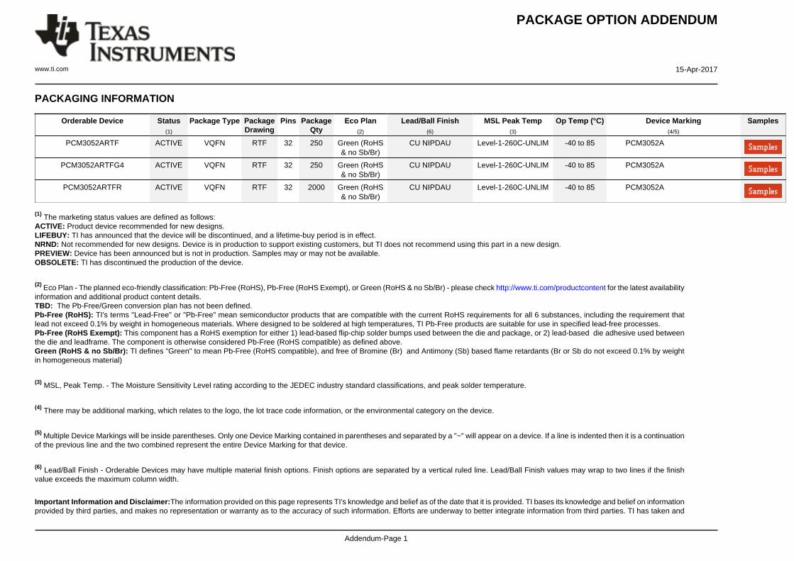
PACKAGING INFORMATION
Orderable Device Status(1)
Package Type PackageDrawing
Pins PackageQty
Eco Plan(2)
Lead/Ball Finish(6)
MSL Peak Temp(3)
Op Temp (°C) Device Marking(4/5)
Samples
PCM3052ARTF ACTIVE VQFN RTF 32 250 Green (RoHS& no Sb/Br)
CU NIPDAU Level-1-260C-UNLIM -40 to 85 PCM3052A
PCM3052ARTFG4 ACTIVE VQFN RTF 32 250 Green (RoHS& no Sb/Br)
CU NIPDAU Level-1-260C-UNLIM -40 to 85 PCM3052A
PCM3052ARTFR ACTIVE VQFN RTF 32 2000 Green (RoHS& no Sb/Br)
CU NIPDAU Level-1-260C-UNLIM -40 to 85 PCM3052A
(1) The marketing status values are defined as follows:ACTIVE: Product device recommended for new designs.LIFEBUY: TI has announced that the device will be discontinued, and a lifetime-buy period is in effect.NRND: Not recommended for new designs. Device is in production to support existing customers, but TI does not recommend using this part in a new design.PREVIEW: Device has been announced but is not in production. Samples may or may not be available.OBSOLETE: TI has discontinued the production of the device.
(2) Eco Plan - The planned eco-friendly classification: Pb-Free (RoHS), Pb-Free (RoHS Exempt), or Green (RoHS & no Sb/Br) - please check http://www.ti.com/productcontent for the latest availabilityinformation and additional product content details.TBD: The Pb-Free/Green conversion plan has not been defined.Pb-Free (RoHS): TI's terms "Lead-Free" or "Pb-Free" mean semiconductor products that are compatible with the current RoHS requirements for all 6 substances, including the requirement thatlead not exceed 0.1% by weight in homogeneous materials. Where designed to be soldered at high temperatures, TI Pb-Free products are suitable for use in specified lead-free processes.Pb-Free (RoHS Exempt): This component has a RoHS exemption for either 1) lead-based flip-chip solder bumps used between the die and package, or 2) lead-based die adhesive used betweenthe die and leadframe. The component is otherwise considered Pb-Free (RoHS compatible) as defined above.Green (RoHS & no Sb/Br): TI defines "Green" to mean Pb-Free (RoHS compatible), and free of Bromine (Br) and Antimony (Sb) based flame retardants (Br or Sb do not exceed 0.1% by weightin homogeneous material)
(3) MSL, Peak Temp. - The Moisture Sensitivity Level rating according to the JEDEC industry standard classifications, and peak solder temperature.
(4) There may be additional marking, which relates to the logo, the lot trace code information, or the environmental category on the device.
(5) Multiple Device Markings will be inside parentheses. Only one Device Marking contained in parentheses and separated by a "~" will appear on a device. If a line is indented then it is a continuationof the previous line and the two combined represent the entire Device Marking for that device.
(6) Lead/Ball Finish - Orderable Devices may have multiple material finish options. Finish options are separated by a vertical ruled line. Lead/Ball Finish values may wrap to two lines if the finishvalue exceeds the maximum column width.
Important Information and Disclaimer:The information provided on this page represents TI's knowledge and belief as of the date that it is provided. TI bases its knowledge and belief on informationprovided by third parties, and makes no representation or warranty as to the accuracy of such information. Efforts are underway to better integrate information from third parties. TI has taken and

PACKAGE OPTION ADDENDUM
www.ti.com 15-Apr-2017
Addendum-Page 2
continues to take reasonable steps to provide representative and accurate information but may not have conducted destructive testing or chemical analysis on incoming materials and chemicals.TI and TI suppliers consider certain information to be proprietary, and thus CAS numbers and other limited information may not be available for release.
In no event shall TI's liability arising out of such information exceed the total purchase price of the TI part(s) at issue in this document sold by TI to Customer on an annual basis.
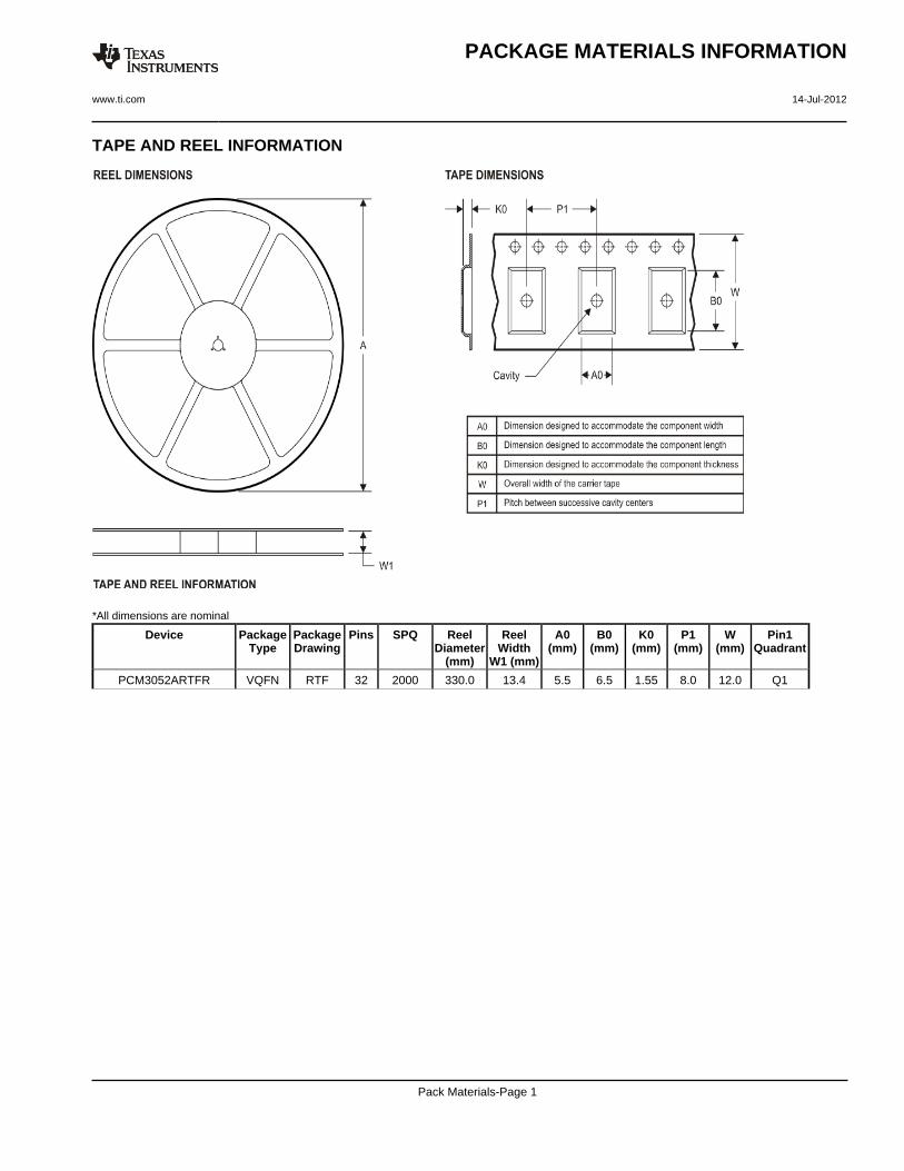
TAPE AND REEL INFORMATION
*All dimensions are nominal
Device PackageType
PackageDrawing
Pins SPQ ReelDiameter
(mm)
ReelWidth
W1 (mm)
A0(mm)
B0(mm)
K0(mm)
P1(mm)
W(mm)
Pin1Quadrant
PCM3052ARTFR VQFN RTF 32 2000 330.0 13.4 5.5 6.5 1.55 8.0 12.0 Q1
PACKAGE MATERIALS INFORMATION
www.ti.com 14-Jul-2012
Pack Materials-Page 1

*All dimensions are nominal
Device Package Type Package Drawing Pins SPQ Length (mm) Width (mm) Height (mm)
PCM3052ARTFR VQFN RTF 32 2000 367.0 367.0 35.0
PACKAGE MATERIALS INFORMATION
www.ti.com 14-Jul-2012
Pack Materials-Page 2

IMPORTANT NOTICE
Texas Instruments Incorporated (TI) reserves the right to make corrections, enhancements, improvements and other changes to itssemiconductor products and services per JESD46, latest issue, and to discontinue any product or service per JESD48, latest issue. Buyersshould obtain the latest relevant information before placing orders and should verify that such information is current and complete.TI’s published terms of sale for semiconductor products (http://www.ti.com/sc/docs/stdterms.htm) apply to the sale of packaged integratedcircuit products that TI has qualified and released to market. Additional terms may apply to the use or sale of other types of TI products andservices.Reproduction of significant portions of TI information in TI data sheets is permissible only if reproduction is without alteration and isaccompanied by all associated warranties, conditions, limitations, and notices. TI is not responsible or liable for such reproduceddocumentation. Information of third parties may be subject to additional restrictions. Resale of TI products or services with statementsdifferent from or beyond the parameters stated by TI for that product or service voids all express and any implied warranties for theassociated TI product or service and is an unfair and deceptive business practice. TI is not responsible or liable for any such statements.Buyers and others who are developing systems that incorporate TI products (collectively, “Designers”) understand and agree that Designersremain responsible for using their independent analysis, evaluation and judgment in designing their applications and that Designers havefull and exclusive responsibility to assure the safety of Designers' applications and compliance of their applications (and of all TI productsused in or for Designers’ applications) with all applicable regulations, laws and other applicable requirements. Designer represents that, withrespect to their applications, Designer has all the necessary expertise to create and implement safeguards that (1) anticipate dangerousconsequences of failures, (2) monitor failures and their consequences, and (3) lessen the likelihood of failures that might cause harm andtake appropriate actions. Designer agrees that prior to using or distributing any applications that include TI products, Designer willthoroughly test such applications and the functionality of such TI products as used in such applications.TI’s provision of technical, application or other design advice, quality characterization, reliability data or other services or information,including, but not limited to, reference designs and materials relating to evaluation modules, (collectively, “TI Resources”) are intended toassist designers who are developing applications that incorporate TI products; by downloading, accessing or using TI Resources in anyway, Designer (individually or, if Designer is acting on behalf of a company, Designer’s company) agrees to use any particular TI Resourcesolely for this purpose and subject to the terms of this Notice.TI’s provision of TI Resources does not expand or otherwise alter TI’s applicable published warranties or warranty disclaimers for TIproducts, and no additional obligations or liabilities arise from TI providing such TI Resources. TI reserves the right to make corrections,enhancements, improvements and other changes to its TI Resources. TI has not conducted any testing other than that specificallydescribed in the published documentation for a particular TI Resource.Designer is authorized to use, copy and modify any individual TI Resource only in connection with the development of applications thatinclude the TI product(s) identified in such TI Resource. NO OTHER LICENSE, EXPRESS OR IMPLIED, BY ESTOPPEL OR OTHERWISETO ANY OTHER TI INTELLECTUAL PROPERTY RIGHT, AND NO LICENSE TO ANY TECHNOLOGY OR INTELLECTUAL PROPERTYRIGHT OF TI OR ANY THIRD PARTY IS GRANTED HEREIN, including but not limited to any patent right, copyright, mask work right, orother intellectual property right relating to any combination, machine, or process in which TI products or services are used. Informationregarding or referencing third-party products or services does not constitute a license to use such products or services, or a warranty orendorsement thereof. Use of TI Resources may require a license from a third party under the patents or other intellectual property of thethird party, or a license from TI under the patents or other intellectual property of TI.TI RESOURCES ARE PROVIDED “AS IS” AND WITH ALL FAULTS. TI DISCLAIMS ALL OTHER WARRANTIES ORREPRESENTATIONS, EXPRESS OR IMPLIED, REGARDING RESOURCES OR USE THEREOF, INCLUDING BUT NOT LIMITED TOACCURACY OR COMPLETENESS, TITLE, ANY EPIDEMIC FAILURE WARRANTY AND ANY IMPLIED WARRANTIES OFMERCHANTABILITY, FITNESS FOR A PARTICULAR PURPOSE, AND NON-INFRINGEMENT OF ANY THIRD PARTY INTELLECTUALPROPERTY RIGHTS. TI SHALL NOT BE LIABLE FOR AND SHALL NOT DEFEND OR INDEMNIFY DESIGNER AGAINST ANY CLAIM,INCLUDING BUT NOT LIMITED TO ANY INFRINGEMENT CLAIM THAT RELATES TO OR IS BASED ON ANY COMBINATION OFPRODUCTS EVEN IF DESCRIBED IN TI RESOURCES OR OTHERWISE. IN NO EVENT SHALL TI BE LIABLE FOR ANY ACTUAL,DIRECT, SPECIAL, COLLATERAL, INDIRECT, PUNITIVE, INCIDENTAL, CONSEQUENTIAL OR EXEMPLARY DAMAGES INCONNECTION WITH OR ARISING OUT OF TI RESOURCES OR USE THEREOF, AND REGARDLESS OF WHETHER TI HAS BEENADVISED OF THE POSSIBILITY OF SUCH DAMAGES.Unless TI has explicitly designated an individual product as meeting the requirements of a particular industry standard (e.g., ISO/TS 16949and ISO 26262), TI is not responsible for any failure to meet such industry standard requirements.Where TI specifically promotes products as facilitating functional safety or as compliant with industry functional safety standards, suchproducts are intended to help enable customers to design and create their own applications that meet applicable functional safety standardsand requirements. Using products in an application does not by itself establish any safety features in the application. Designers mustensure compliance with safety-related requirements and standards applicable to their applications. Designer may not use any TI products inlife-critical medical equipment unless authorized officers of the parties have executed a special contract specifically governing such use.Life-critical medical equipment is medical equipment where failure of such equipment would cause serious bodily injury or death (e.g., lifesupport, pacemakers, defibrillators, heart pumps, neurostimulators, and implantables). Such equipment includes, without limitation, allmedical devices identified by the U.S. Food and Drug Administration as Class III devices and equivalent classifications outside the U.S.TI may expressly designate certain products as completing a particular qualification (e.g., Q100, Military Grade, or Enhanced Product).Designers agree that it has the necessary expertise to select the product with the appropriate qualification designation for their applicationsand that proper product selection is at Designers’ own risk. Designers are solely responsible for compliance with all legal and regulatoryrequirements in connection with such selection.Designer will fully indemnify TI and its representatives against any damages, costs, losses, and/or liabilities arising out of Designer’s non-compliance with the terms and provisions of this Notice.
Mailing Address: Texas Instruments, Post Office Box 655303, Dallas, Texas 75265Copyright © 2017, Texas Instruments Incorporated