Embed Size (px)
Citation preview
Data Sheet
FEATURES:
• High Gain: – Typically 29 dB gain across 2.4-2.5 GHz– Typically 29-26 dB gain across 4.9-5.8 GHz
• High linear output power: – >25 dBm P1dB (Pulsed single-tone signal) across
2.4-2.5 GHz – Meets 802.11b OFDM ACPR requirement up to
23.5 dBm across 2.4-2.5 GHz– Meets 802.11g OFDM ACPR requirement up to
23 dBm across 2.4-2.5 GHz– Added EVM ~4% up to 19 dBm for
54 Mbps 802.11g signal across 2.4-2.5 GHz– >24 dBm P1dB across 4.9-5.8 GHz– Meets 802.11a OFDM ACPR requirement up to
22.5 dBm across 4.9-5.8 GHz– Added EVM ~4% up to 18 dBm for
54 Mbps 802.11a signal across 4.9-5.8 GHz• High power-added efficiency/Low operating
current for 802.11a/b/g applications– ~160 mA @ POUT = 19 dBm for 802.11g– ~235 mA @ POUT = 23.5 dBm for 802.11b– ~270 mA @ POUT = 18 dBm for 802.11a
• Built-in Ultra-low IREF power-up/down control– IREF < 2 mA
• High-speed power-up/down– Turn on/off time (10%-90%) <100 ns– Typical power-up/down delay with driver delay
included <200 ns
• High temperature stability– ~1 dB gain/power variation between 0°C to +85°C
across 2.4-2.5 GHz– ~3/1 dB gain/max linear power variation between
0°C to +85°C across 4.9-5.8 GHz– ±0.5 dB detector variation between 0°C to +85°C
• Low shut-down current (< 2 µA)• 20 dB dynamic range on-chip power detection• Built-in input/output matching• Packages available
– 16-contact LGA package (4mm x 4mm)• All non-Pb (lead-free) devices are ROHS compliant.
APPLICATIONS:
• WLAN (IEEE 802.11a/g/b)• Japanese WLAN• HyperLAN2• Multimedia• Home RF• Cordless phones
2.4-2.5 GHz / 4.9-5.8 GHz Dual-Band Power Amplifier Module SST13LP05
SST13LP052.4 - 2.5 GHz / 4.9-5.8 GHz Dual-Band Power Amplifier
PRODUCT DESCRIPTION
The SST13LP05 is a fully matched, dual-band poweramplifier module (PAM) based on the highly-reliable InGaP/GaAs HBT technology. This PAM provides excellent RFperformance, temperature-stable power detectors, andlow-current analog on/off control interfaces. TheSST13LP05 provides stable RF and power detector perfor-mance over a large VCC power supply variation, with anultra-low shut-down current.
With a near-zero Rest of Bill of Materials (RBOM), theSST13LP05 is designed for 802.11a/b/g applications cov-ering frequency bands 2.4-2.5 GHz and 4.9-5.8 GHz forU.S., European, and Japanese markets.
The SST13LP05 has excellent linearity, typically 4% addedError Vector Magnitude (EVM) at 19 dBm output power.This output power is essential for 54 Mbps 802.11g opera-tion while meeting 802.11g spectrum mask at 23 dBm and802.11b spectrum mask at 23.5 dBm. For 802.11a opera-
tion, the SST13LP05 typically demonstrates <4% addedEVM at 18 dBm output power while meeting 802.11a spec-trum mask at 22.5 dBm.
The SST13LP05 also has wide-range (>20 dB), tempera-ture-stable (±0.5 dB across 0°C to +85°C), directionally-coupled, power detectors which provide a reliable and cost-effective solution to board-level power control. The device’sanalog on/off control can be driven by an analog or digitalcontrol signal from either a transceiver or baseband chip.
These features, coupled with low operating current, makethe SST13LP05 ideal for the final stage power amplifica-tion in both battery-powered 802.11a/b/g WLAN trans-mitters and access point applications.
The SST13LP05 is offered in a 16-contact LGA package.See Figure 2 for pin assignments and Table 1 for pindescriptions.
©2008 Silicon Storage Technology, Inc.S71318-02-000 02/091
The SST logo and SuperFlash are registered Trademarks of Silicon Storage Technology, Inc.These specifications are subject to change without notice.
Data Sheet
2.4-2.5 GHz / 4.9-5.8 GHz Dual-Band Power AmplifierSST13LP05
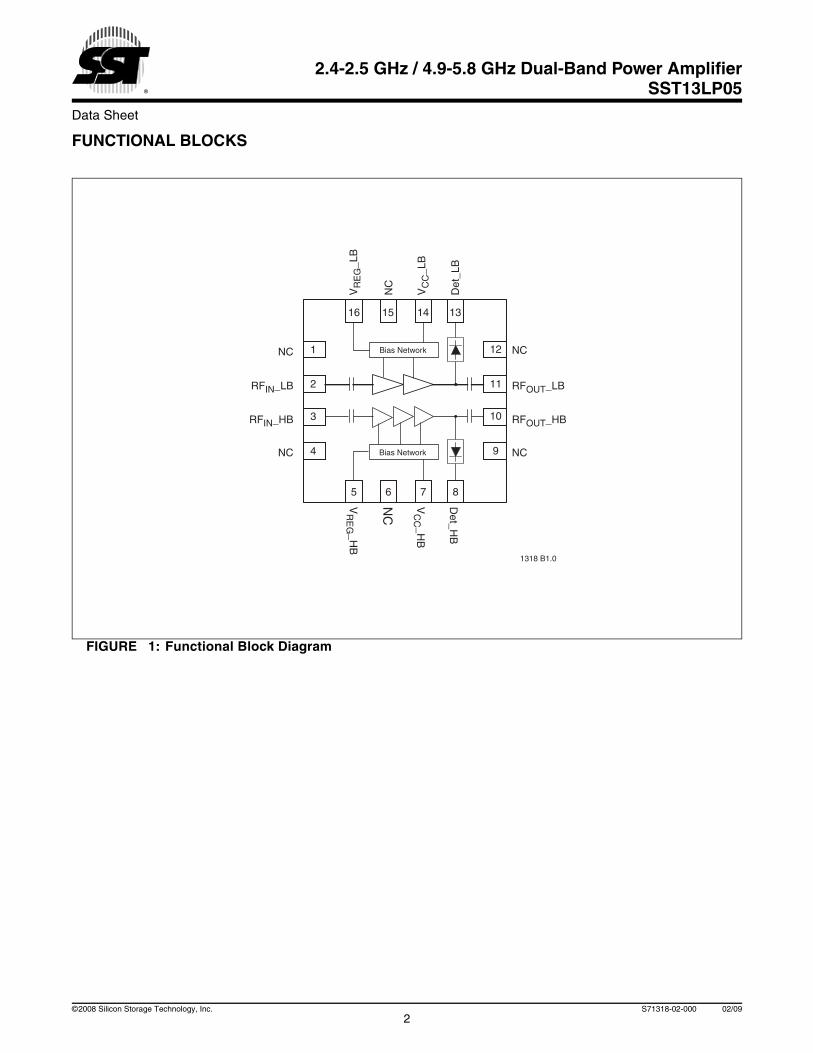
FUNCTIONAL BLOCKS
FIGURE 1: Functional Block Diagram
VR
EG
_LB
VC
C_L
B
NC
Det
_LB
V
RE
G_H
B
NC
VC
C_H
B
Det_H
BNC
RFOUT_LB
RFOUT_HB
NC
NC
RFIN_LB
RFIN_HB
NC
1318 B1.0
5 6 8
16 15 14
9
11
12
10
13
2
1
4
3
7
Bias Network
Bias Network
©2008 Silicon Storage Technology, Inc. S71318-02-000 02/092
Data Sheet
2.4-2.5 GHz / 4.9-5.8 GHz Dual-Band Power AmplifierSST13LP05
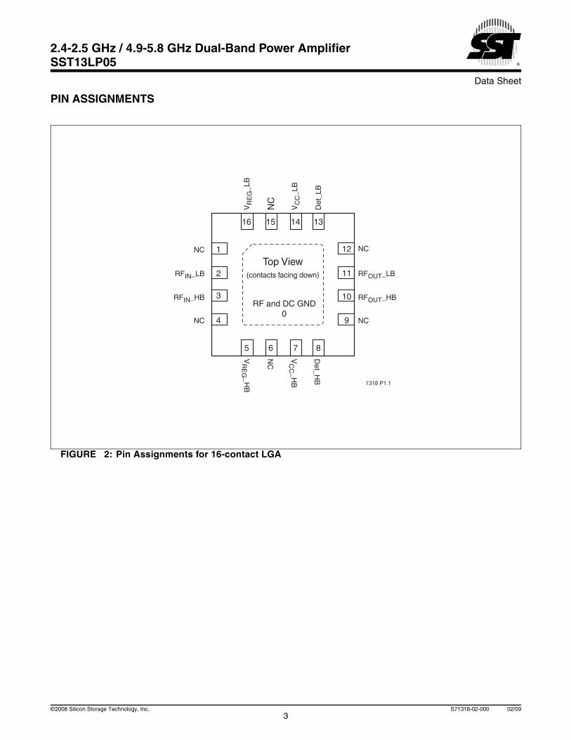
PIN ASSIGNMENTS
FIGURE 2: Pin Assignments for 16-contact LGA
VR
EG
_LB
VC
C_L
B
NC
Det
_LB
V
RE
G_H
B
NC
VC
C_H
B
Det_H
BNC
RFOUT_LB
RFOUT_HB
NC
NC
RFIN_LB
RFIN_HB
NC
1318 P1.1
5 6 8
16 15 14
9
11
12
10
13
2
1
4
3
7
Top View(contacts facing down)
RF and DC GND0
3©2008 Silicon Storage Technology, Inc. S71318-02-000 02/09
Data Sheet
2.4-2.5 GHz / 4.9-5.8 GHz Dual-Band Power AmplifierSST13LP05
PIN DESCRIPTIONS
TABLE 1: Pin Description
Symbol Pin No. Pin Name Type Function
GND 0 Ground Ground Pad
NC 1 No Connection Unconnected Pin
RFIN_LB 2 I 50Ω Matched RF Input for Low Band, AC coupled
RFIN_HB 3 I 50Ω Matched RF Input for High Band, AC coupled
NC 4 No Connection Unconnected Pin
VREG_HB 5 Power Supply PWR Analog current control for High Band
NC 6 No Connection Unconnected Pin
VCC_HB 7 Power Supply PWR VCC Power Supply for High Band
DET_HB 8 O Detector Voltage Output for High Band
NC 9 No Connection Unconnected Pin
RFOUT_HB 10 Power Supply O/PWR 50Ω Matched RF output for High Band
RFOUT_LB 11 Power Supply O/PWR 50Ω Matched RF output for Low Band
NC 12 No Connection Unconnected Pin
DET_LB 13 O Detector Voltage Output for Low Band
VCC_LB 14 Power Supply PWR VCC Power Supply for Low Band
NC 15 No Connection Unconnected Pin
VREG_LB 16 Power Supply PWR Analog current control for Low BandT1.0 1318
©2008 Silicon Storage Technology, Inc. S71318-02-000 02/094
Data Sheet
2.4-2.5 GHz / 4.9-5.8 GHz Dual-Band Power AmplifierSST13LP05
ELECTRICAL SPECIFICATIONS
The AC and DC specifications for the power amplifier interface signals. Refer to Tables 2 and 4 for the DC voltage and currentspecifications. Refer to Figures 3 through 22 for the RF performance.
Absolute Maximum Stress Ratings Applied conditions greater than those listed under “Absolute Maximum Stress Rat-ings” may cause permanent damage to the device. This is a stress rating only and functional operation of the device at theseconditions or conditions greater than those defined in the operational sections of this data sheet is not implied. Exposure toabsolute maximum stress rating conditions may affect device reliability.
Supply Voltage (VCC) . . . . . . . . . . . . . . . . . . . . . . . . . . . . . . . . . . . . . . . . . . . . . . . . . . . . . . . . . . . . . . -0.3V to +3.6VReference Voltage (VREF) . . . . . . . . . . . . . . . . . . . . . . . . . . . . . . . . . . . . . . . . . . . . . . . . . . . . . . . . . . -0.3V to +3.3VDC supply current (ICC) . . . . . . . . . . . . . . . . . . . . . . . . . . . . . . . . . . . . . . . . . . . . . . . . . . . . . . . . . . . . . . . . . 400 mAOperating Temperature (TA) . . . . . . . . . . . . . . . . . . . . . . . . . . . . . . . . . . . . . . . . . . . . . . . . . . . . . . . . -40ºC to +85ºCStorage Temperature (TSTG) . . . . . . . . . . . . . . . . . . . . . . . . . . . . . . . . . . . . . . . . . . . . . . . . . . . . . . -40ºC to +120ºCMaximum Junction Temperature (TJ) . . . . . . . . . . . . . . . . . . . . . . . . . . . . . . . . . . . . . . . . . . . . . . . . . . . . . . . +150ºC
5©2008 Silicon Storage Technology, Inc. S71318-02-000 02/09
Data Sheet
2.4-2.5 GHz / 4.9-5.8 GHz Dual-Band Power AmplifierSST13LP05
For 802.11b/g Operation
TABLE 2: DC Electrical Characteristics
Symbol Parameter Min. Typ Max. Unit
VCC Supply Voltage 3.0 3.3 3.6 V
ICC Supply Current
for 802.11g, 19 dBm 160 mA
for 802.11b, 23.5 dBm 235 mA
IREG Analog control current at On state 2 mA
VREG Reference Voltage 2.95 VT2.0 1318
TABLE 3: AC Electrical Characteristics for Configuration
Symbol Parameter Min. Typ Max. Unit
FL-U Frequency range 2.4 2.5 GHz
G Small signal gain 28 29 dB
GVAR1 Gain variation over temperature 0°C – 85°C -1 1 dB
GVAR2 Gain flatness over any 50 MHz bandwidth -0.3 0.3 dB
ACPR Meet 11b spectrum mask 22 23 dBm
Meet 11g OFDM 54 Mbps spectrum mask 22 23 dBm
Added EVM POUT = 19 dBm with 54Mbps -28 dB
11g OFDM signal when operating at 3.3V Vcc 4 %
2f, 3f, 4f, 5f Harmonics at POUT = 20 dBm -50 dBc
Spurious non-harmonics at POUT = 20 dBm -60 dBc
In/Out return loss at 50 Ω nominal impedance 6 dBT3.0 1318
©2008 Silicon Storage Technology, Inc. S71318-02-000 02/096
Data Sheet
2.4-2.5 GHz / 4.9-5.8 GHz Dual-Band Power AmplifierSST13LP05
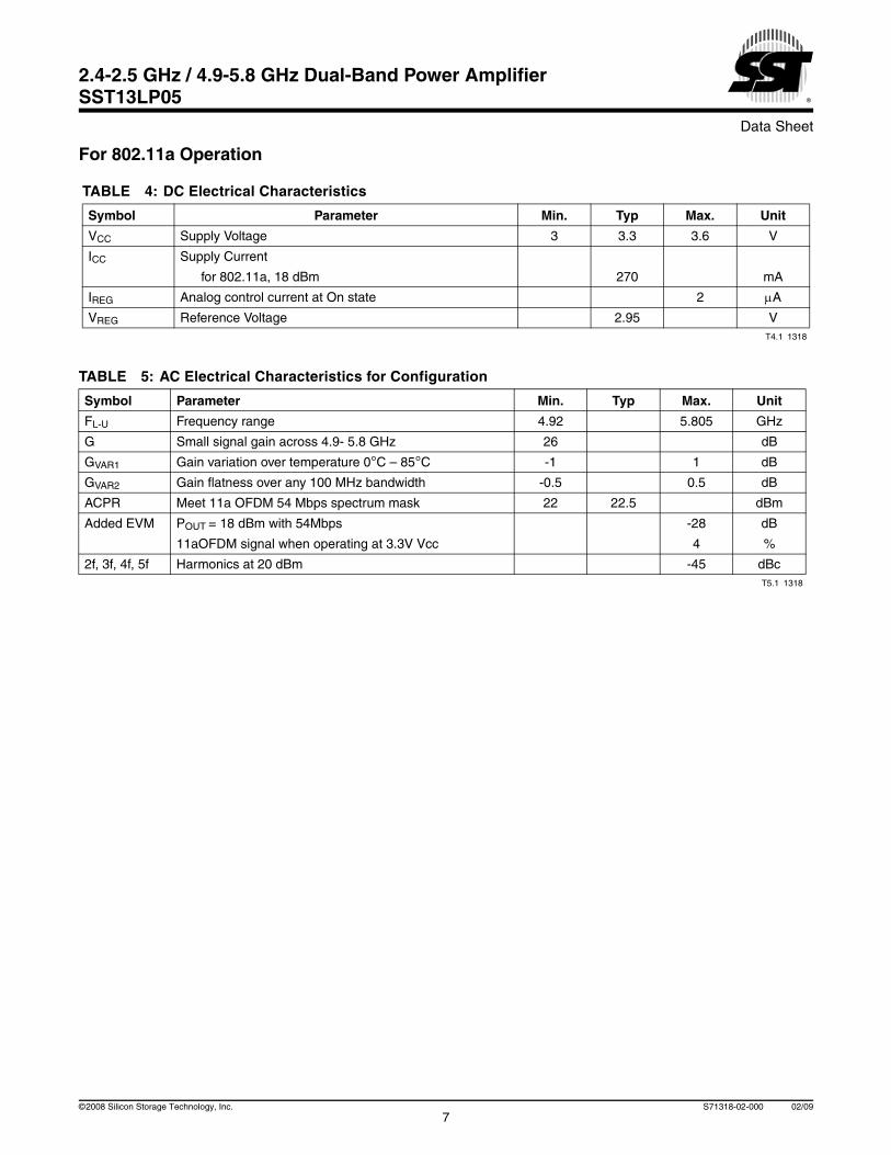
For 802.11a Operation
TABLE 4: DC Electrical Characteristics
Symbol Parameter Min. Typ Max. Unit
VCC Supply Voltage 3 3.3 3.6 V
ICC Supply Current
for 802.11a, 18 dBm 270 mA
IREG Analog control current at On state 2 μA
VREG Reference Voltage 2.95 VT4.1 1318
TABLE 5: AC Electrical Characteristics for Configuration
Symbol Parameter Min. Typ Max. Unit
FL-U Frequency range 4.92 5.805 GHz
G Small signal gain across 4.9- 5.8 GHz 26 dB
GVAR1 Gain variation over temperature 0°C – 85°C -1 1 dB
GVAR2 Gain flatness over any 100 MHz bandwidth -0.5 0.5 dB
ACPR Meet 11a OFDM 54 Mbps spectrum mask 22 22.5 dBm
Added EVM POUT = 18 dBm with 54Mbps -28 dB
11aOFDM signal when operating at 3.3V Vcc 4 %
2f, 3f, 4f, 5f Harmonics at 20 dBm -45 dBcT5.1 1318
7©2008 Silicon Storage Technology, Inc. S71318-02-000 02/09
Data Sheet
2.4-2.5 GHz / 4.9-5.8 GHz Dual-Band Power AmplifierSST13LP05
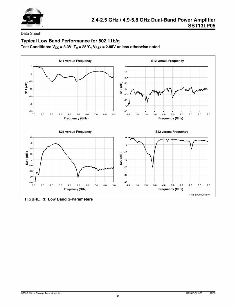
Typical Low Band Performance for 802.11b/gTest Conditions: VCC = 3.3V, TA = 25°C, VREF = 2.95V unless otherwise noted
FIGURE 3: Low Band S-Parameters
1318 SParmLowB.0
S11 versus Frequency
-30
-25
-20
-15
-10
-5
0
0.0 1.0 2.0 3.0 4.0 5.0 6.0 7.0 8.0 9.0
Frequency (GHz)
S11
(d
B)
S12 versus Frequency
-80
-70
-60
-50
-40
-30
-20
-10
0
0.0 1.0 2.0 3.0 4.0 5.0 6.0 7.0 8.0 9.0
Frequency (GHz)S
12 (
dB
)
S21 versus Frequency
-40
-30
-20
-10
0
10
20
30
40
0.0 1.0 2.0 3.0 4.0 5.0 6.0 7.0 8.0 9.0
Frequency (GHz)
S21 (
dB
)
S22 versus Frequency
-30
-25
-20
-15
-10
-5
0
0.0 1.0 2.0 3.0 4.0 5.0 6.0 7.0 8.0 9.0
Frequency (GHz)
S22
(d
B)
©2008 Silicon Storage Technology, Inc. S71318-02-000 02/098
Data Sheet
2.4-2.5 GHz / 4.9-5.8 GHz Dual-Band Power AmplifierSST13LP05
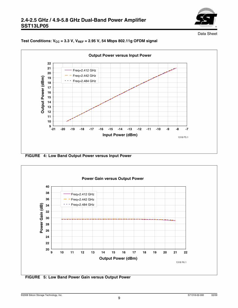
Test Conditions: VCC = 3.3 V, VREF = 2.95 V, 54 Mbps 802.11g OFDM signal
FIGURE 4: Low Band Output Power versus Input Power
FIGURE 5: Low Band Power Gain versus Output Power
Output Power versus Input Power
9
10
11
12
13
14
15
16
17
18
19
20
21
22
-21 -20 -19 -18 -17 -16 -15 -14 -13 -12 -11 -10 -9 -8 -7
Input Power (dBm)
Ou
tpu
t P
ow
er (
dB
m)
Freq=2.412 GHz
Freq=2.442 GHz
Freq=2.484 GHz
1318 F5.1
Power Gain versus Output Power
20
22
24
26
28
30
32
34
36
38
40
9 10 11 12 13 14 15 16 17 18 19 20 21 22
Output Power (dBm)
Po
wer
Gai
n (
dB
)
Freq=2.412 GHz
Freq=2.442 GHz
Freq=2.484 GHz
1318 F6.1
9©2008 Silicon Storage Technology, Inc. S71318-02-000 02/09
Data Sheet
2.4-2.5 GHz / 4.9-5.8 GHz Dual-Band Power AmplifierSST13LP05
FIGURE 6: Low Band Supply Current versus Output Power
FIGURE 7: Low Band PAE versus Output Power
Supply Current versus Output Power
80
90
100
110
120
130
140
150
160
170
180
190
200
9 10 11 12 13 14 15 16 17 18 19 20 21 22
Output Power (dBm)
Su
pp
ly C
urr
ent
(mA
)
Freq=2.412 GHz
Freq=2.442 GHz
Freq=2.484 GHz
1318 F7.1
PAE versus Output Power
0
2
4
6
8
10
12
14
16
18
20
22
24
9 10 11 12 13 14 15 16 17 18 19 20 21 22
Output Power (dBm)
PA
E (
%)
Freq=2.412 GHz
Freq=2.442 GHz
Freq=2.484 GHz
1318 F8.1
©2008 Silicon Storage Technology, Inc. S71318-02-000 02/0910
Data Sheet
2.4-2.5 GHz / 4.9-5.8 GHz Dual-Band Power AmplifierSST13LP05
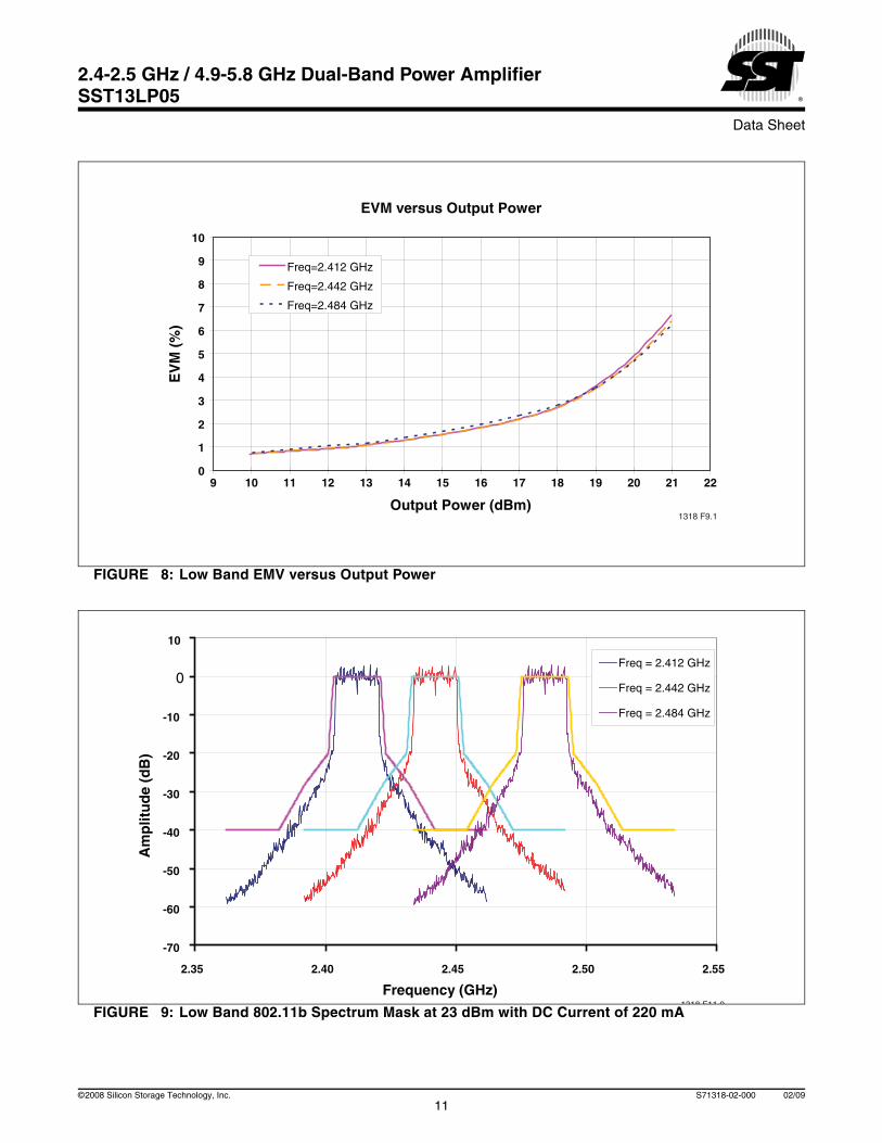
FIGURE 8: Low Band EMV versus Output Power
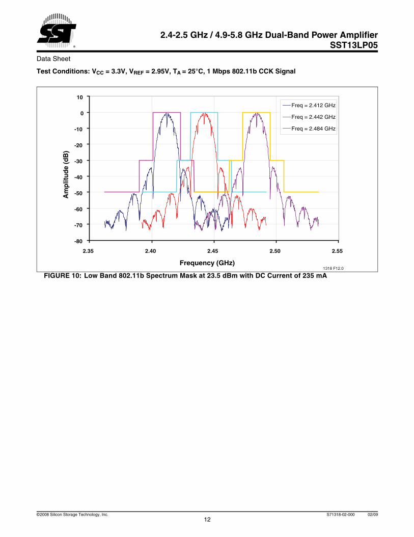
FIGURE 9: Low Band 802.11b Spectrum Mask at 23 dBm with DC Current of 220 mA
EVM versus Output Power
0
1
2
3
4
5
6
7
8
9
10
9 10 11 12 13 14 15 16 17 18 19 20 21 22
Output Power (dBm)
EV
M (
%)
Freq=2.412 GHz
Freq=2.442 GHz
Freq=2.484 GHz
1318 F9.1
-70
-60
-50
-40
-30
-20
-10
0
10
2.35 2.40 2.45 2.50 2.55
Frequency (GHz)
Am
plit
ud
e (d
B)
Freq = 2.412 GHz
Freq = 2.442 GHz
Freq = 2.484 GHz
1318 F11 0
11©2008 Silicon Storage Technology, Inc. S71318-02-000 02/09
Data Sheet
2.4-2.5 GHz / 4.9-5.8 GHz Dual-Band Power AmplifierSST13LP05
Test Conditions: VCC = 3.3V, VREF = 2.95V, TA = 25°C, 1 Mbps 802.11b CCK Signal
FIGURE 10: Low Band 802.11b Spectrum Mask at 23.5 dBm with DC Current of 235 mA
-80
-70
-60
-50
-40
-30
-20
-10
0
10
2.35 2.40 2.45 2.50 2.55
Frequency (GHz)
Am
plit
ud
e (d
B)
Freq = 2.412 GHz
Freq = 2.442 GHz
Freq = 2.484 GHz
1318 F12.0
©2008 Silicon Storage Technology, Inc. S71318-02-000 02/0912
Data Sheet
2.4-2.5 GHz / 4.9-5.8 GHz Dual-Band Power AmplifierSST13LP05
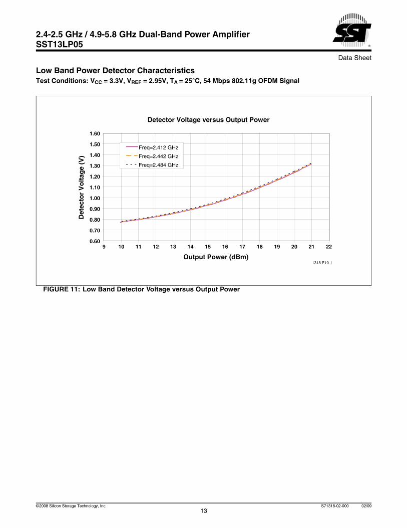
Low Band Power Detector CharacteristicsTest Conditions: VCC = 3.3V, VREF = 2.95V, TA = 25°C, 54 Mbps 802.11g OFDM Signal
FIGURE 11: Low Band Detector Voltage versus Output Power
Detector Voltage versus Output Power
0.60
0.70
0.80
0.90
1.00
1.10
1.20
1.30
1.40
1.50
1.60
9 10 11 12 13 14 15 16 17 18 19 20 21 22
Output Power (dBm)
Det
ecto
r V
olt
age
(V)
Freq=2.412 GHz
Freq=2.442 GHz
Freq=2.484 GHz
1318 F10.1
13©2008 Silicon Storage Technology, Inc. S71318-02-000 02/09
Data Sheet
2.4-2.5 GHz / 4.9-5.8 GHz Dual-Band Power AmplifierSST13LP05
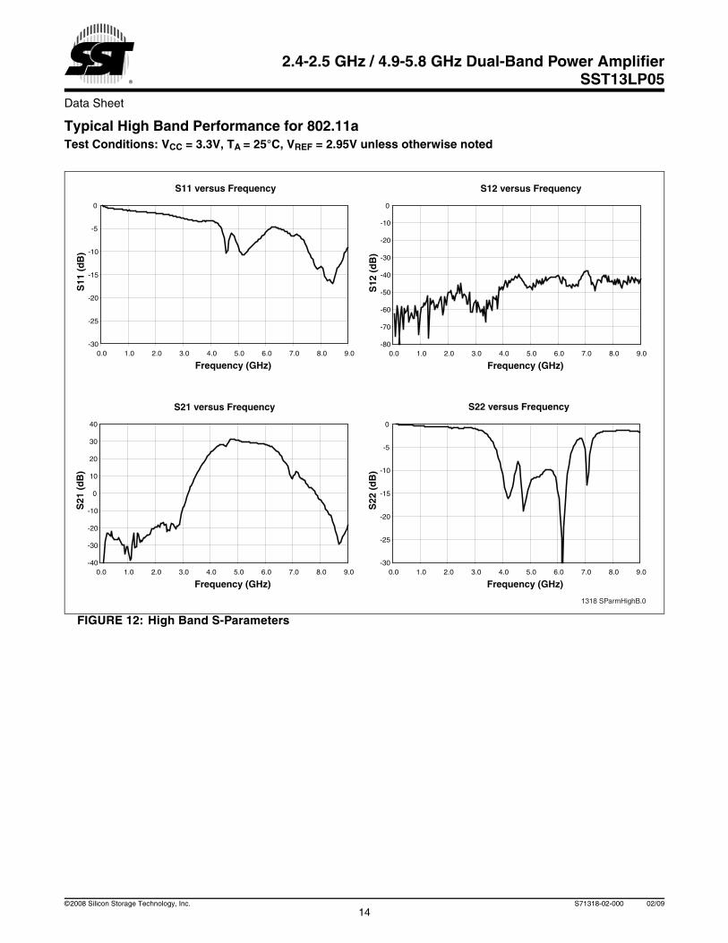
Typical High Band Performance for 802.11aTest Conditions: VCC = 3.3V, TA = 25°C, VREF = 2.95V unless otherwise noted
FIGURE 12: High Band S-Parameters
1318 SParmHighB.0
S11 versus Frequency
-30
-25
-20
-15
-10
-5
0
0.0 1.0 2.0 3.0 4.0 5.0 6.0 7.0 8.0 9.0
Frequency (GHz)
S11
(d
B)
S12 versus Frequency
-80
-70
-60
-50
-40
-30
-20
-10
0
0.0 1.0 2.0 3.0 4.0 5.0 6.0 7.0 8.0 9.0
Frequency (GHz)S
12 (
dB
)
S21 versus Frequency
-40
-30
-20
-10
0
10
20
30
40
0.0 1.0 2.0 3.0 4.0 5.0 6.0 7.0 8.0 9.0
Frequency (GHz)
S21
(d
B)
S22 versus Frequency
-30
-25
-20
-15
-10
-5
0
0.0 1.0 2.0 3.0 4.0 5.0 6.0 7.0 8.0 9.0
Frequency (GHz)
S22
(d
B)
©2008 Silicon Storage Technology, Inc. S71318-02-000 02/0914
Data Sheet
2.4-2.5 GHz / 4.9-5.8 GHz Dual-Band Power AmplifierSST13LP05
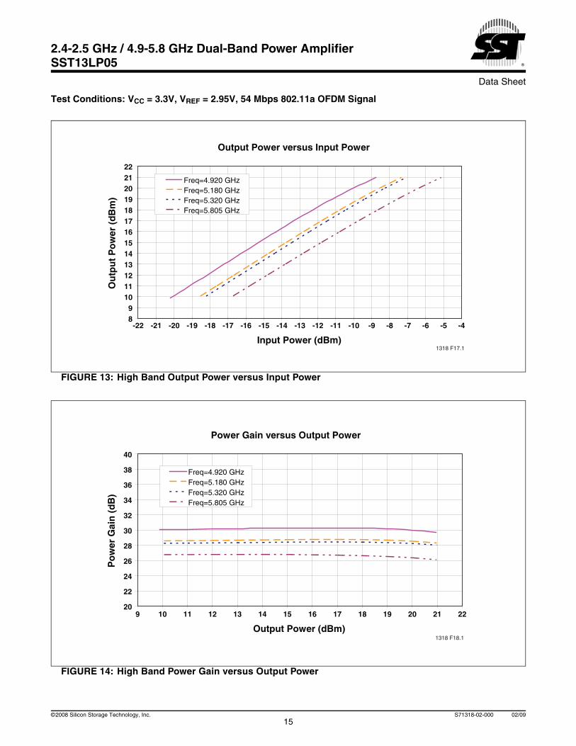
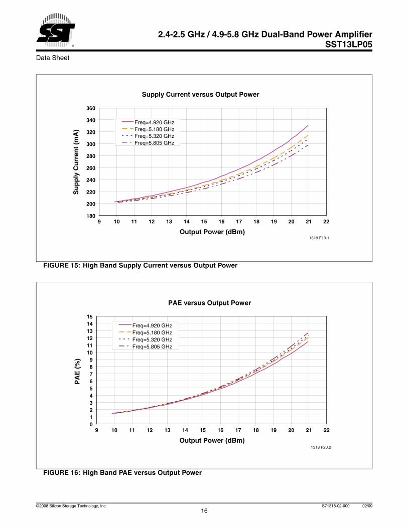
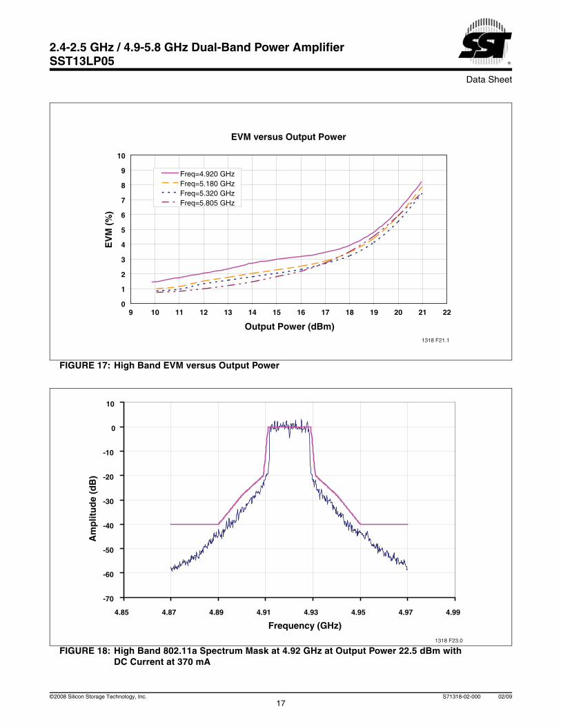
Test Conditions: VCC = 3.3V, VREF = 2.95V, 54 Mbps 802.11a OFDM Signal
FIGURE 13: High Band Output Power versus Input Power
FIGURE 14: High Band Power Gain versus Output Power
Output Power versus Input Power
89
10111213141516171819202122
-22 -21 -20 -19 -18 -17 -16 -15 -14 -13 -12 -11 -10 -9 -8 -7 -6 -5 -4
Input Power (dBm)
Ou
tpu
t P
ow
er (
dB
m)
Freq=4.920 GHzFreq=5.180 GHzFreq=5.320 GHzFreq=5.805 GHz
1318 F17.1
Power Gain versus Output Power
20
22
24
26
28
30
32
34
36
38
40
9 10 11 12 13 14 15 16 17 18 19 20 21 22
Output Power (dBm)
Po
wer
Gai
n (
dB
)
Freq=4.920 GHzFreq=5.180 GHzFreq=5.320 GHzFreq=5.805 GHz
1318 F18.1
15©2008 Silicon Storage Technology, Inc. S71318-02-000 02/09
Data Sheet
2.4-2.5 GHz / 4.9-5.8 GHz Dual-Band Power AmplifierSST13LP05
FIGURE 15: High Band Supply Current versus Output Power
FIGURE 16: High Band PAE versus Output Power
Supply Current versus Output Power
180
200
220
240
260
280
300
320
340
360
9 10 11 12 13 14 15 16 17 18 19 20 21 22
Output Power (dBm)
Su
pp
ly C
urr
ent
(mA
)
Freq=4.920 GHzFreq=5.180 GHzFreq=5.320 GHzFreq=5.805 GHz
1318 F19.1
PAE versus Output Power
0123456789
101112131415
9 10 11 12 13 14 15 16 17 18 19 20 21 22
Output Power (dBm)
PA
E (
%)
Freq=4.920 GHzFreq=5.180 GHzFreq=5.320 GHzFreq=5.805 GHz
1318 F20.2
©2008 Silicon Storage Technology, Inc. S71318-02-000 02/0916
Data Sheet
2.4-2.5 GHz / 4.9-5.8 GHz Dual-Band Power AmplifierSST13LP05
FIGURE 17: High Band EVM versus Output Power
FIGURE 18: High Band 802.11a Spectrum Mask at 4.92 GHz at Output Power 22.5 dBm with DC Current at 370 mA
EVM versus Output Power
0
1
2
3
4
5
6
7
8
9
10
9 10 11 12 13 14 15 16 17 18 19 20 21 22
Output Power (dBm)
EV
M (
%)
Freq=4.920 GHzFreq=5.180 GHzFreq=5.320 GHzFreq=5.805 GHz
1318 F21.1
-70
-60
-50
-40
-30
-20
-10
0
10
4.85 4.87 4.89 4.91 4.93 4.95 4.97 4.99
Frequency (GHz)
Am
plit
ud
e (d
B)
1318 F23.0
17©2008 Silicon Storage Technology, Inc. S71318-02-000 02/09
Data Sheet
2.4-2.5 GHz / 4.9-5.8 GHz Dual-Band Power AmplifierSST13LP05
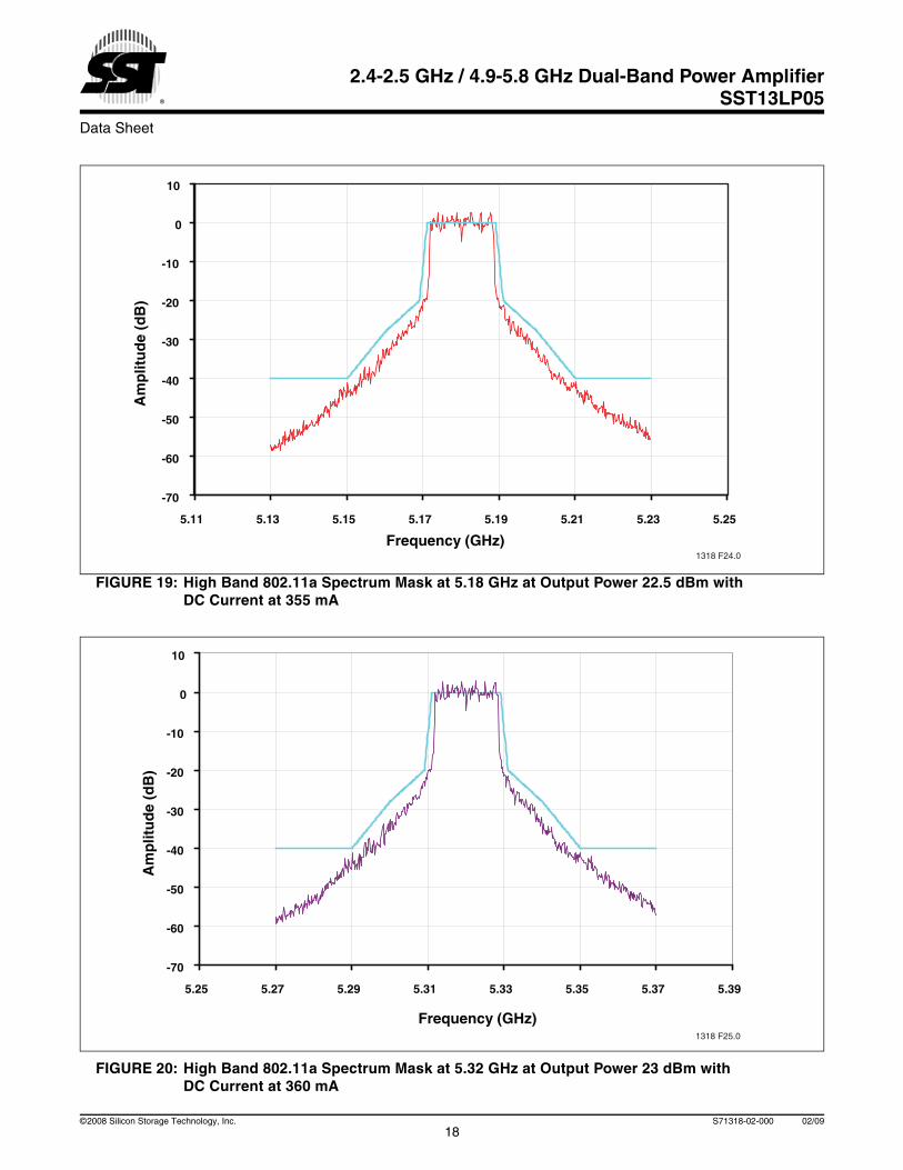
FIGURE 19: High Band 802.11a Spectrum Mask at 5.18 GHz at Output Power 22.5 dBm with DC Current at 355 mA
FIGURE 20: High Band 802.11a Spectrum Mask at 5.32 GHz at Output Power 23 dBm with DC Current at 360 mA
-70
-60
-50
-40
-30
-20
-10
0
10
5.11 5.13 5.15 5.17 5.19 5.21 5.23 5.25
Frequency (GHz)
Am
plit
ud
e (d
B)
1318 F24.0
-70
-60
-50
-40
-30
-20
-10
0
10
5.25 5.27 5.29 5.31 5.33 5.35 5.37 5.39
Frequency (GHz)
Am
plit
ud
e (d
B)
1318 F25.0
©2008 Silicon Storage Technology, Inc. S71318-02-000 02/0918
Data Sheet
2.4-2.5 GHz / 4.9-5.8 GHz Dual-Band Power AmplifierSST13LP05
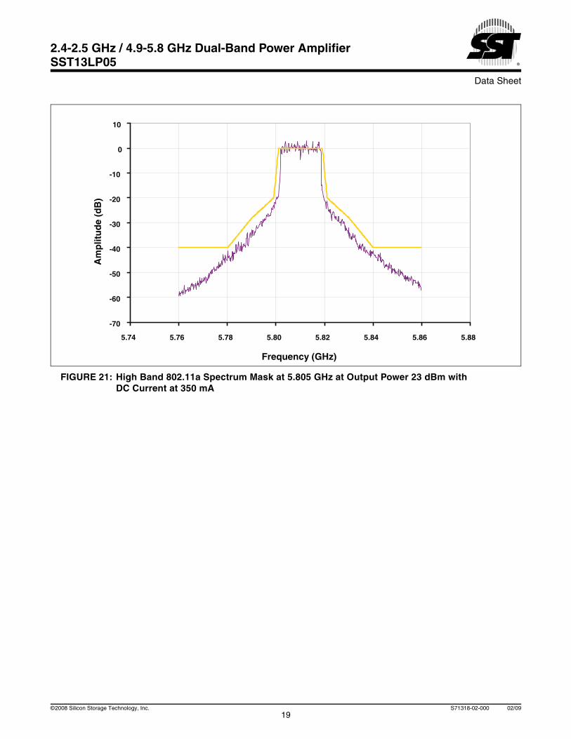
FIGURE 21: High Band 802.11a Spectrum Mask at 5.805 GHz at Output Power 23 dBm with DC Current at 350 mA
-70
-60
-50
-40
-30
-20
-10
0
10
5.74 5.76 5.78 5.80 5.82 5.84 5.86 5.88
Frequency (GHz)
Am
plit
ud
e (d
B)
19©2008 Silicon Storage Technology, Inc. S71318-02-000 02/09
Data Sheet
2.4-2.5 GHz / 4.9-5.8 GHz Dual-Band Power AmplifierSST13LP05
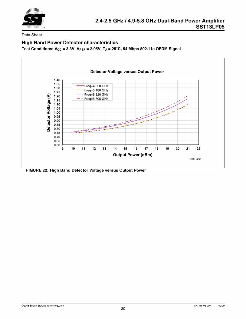
High Band Power Detector characteristicsTest Conditions: VCC = 3.3V, VREF = 2.95V, TA = 25°C, 54 Mbps 802.11a OFDM Signal
FIGURE 22: High Band Detector Voltage versus Output Power
Detector Voltage versus Output Power
0.600.650.700.750.800.850.900.951.001.051.101.151.201.251.301.351.40
9 10 11 12 13 14 15 16 17 18 19 20 21 22
Output Power (dBm)
Det
ecto
r V
olt
age
(V)
Freq=4.920 GHzFreq=5.180 GHzFreq=5.320 GHzFreq=5.805 GHz
1318 F22.2
©2008 Silicon Storage Technology, Inc. S71318-02-000 02/0920
Data Sheet
2.4-2.5 GHz / 4.9-5.8 GHz Dual-Band Power AmplifierSST13LP05
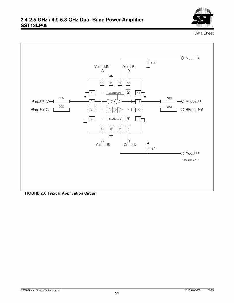
FIGURE 23: Typical Application Circuit
1318 app_cir 1.1
RFIN_LB50Ω
VCC_HB
RFOUT_HB
1 µF
RFIN_HB50Ω 50Ω
RFOUT_LB50Ω
DET_HBVREF_HB
VCC_LB1 µF
VREF_LB DET_LB
5 6 8
16 15 14
9
11
12
10
13
2
1
4
3
7
Bias Network
Bias Network
21©2008 Silicon Storage Technology, Inc. S71318-02-000 02/09
Data Sheet
2.4-2.5 GHz / 4.9-5.8 GHz Dual-Band Power AmplifierSST13LP05
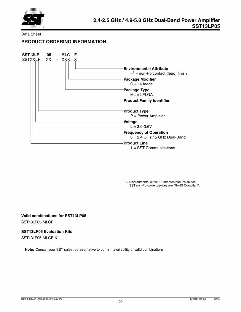
PRODUCT ORDERING INFORMATION
Valid combinations for SST13LP05
SST13LP05-MLCF
SST13LP05 Evaluation Kits
SST13LP05-MLCF-K
Note: Consult your SST sales representative to confirm availability of valid combinations.
SST13LP 05 - MLC FSSTXXLP XX - XXX X
Environmental AttributeF1 = non-Pb contact (lead) finish
Package ModifierC = 16 leads
Package TypeML = LFLGA
Product Family Identifier
Product TypeP = Power Amplifier
VoltageL = 3.0-3.6V
Frequency of Operation3 = 2.4 GHz / 5 GHz Dual-Band
Product Line1 = SST Communications
1. Environmental suffix “F” denotes non-Pb solder. SST non-Pb solder devices are “RoHS Compliant”.
©2008 Silicon Storage Technology, Inc. S71318-02-000 02/0922
Data Sheet
2.4-2.5 GHz / 4.9-5.8 GHz Dual-Band Power AmplifierSST13LP05
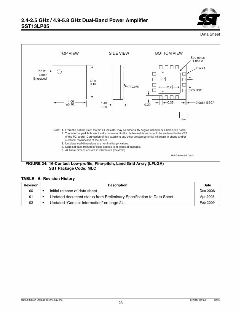
FIGURE 24: 16-Contact Low-profile, Fine-pitch, Land Grid Array (LFLGA)SST Package Code: MLC
TABLE 6: Revision History
Revision Description Date
00 • Initial release of data sheet. Dec 2006
01 • Updated document status from Preliminary Specification to Data Sheet Apr 2008
02 • Updated “Contact Information” on page 24. Feb 2009
Note: 1. From the bottom view, the pin #1 indicator may be either a 45-degree chamfer or a half-circle notch. 2. The external paddle is electrically connected to the die back-side and should be soldered to the VSS of the PC board. Connection of this paddle to any other voltage potential will result in shorts and/or electrical malfunction of the device. 3. Untoleranced dimensions are nominal target values. 4. Land set back from body edge applies to all lands of package. 5. All linear dimensions are in millimeters (max/min). 16-LGA-4x4-MLC-0.0
2.7
Pin #1
0.0684 BSC4
2.7
1.401.20
Pin #1Laser
Engraved
TOP VIEW BOTTOM VIEWSIDE VIEW
1mm
0.35
0.65 BSC
0.39
4.00 ±0.10
4.00 ±0.10
See notes1 and 2
0.075
23©2008 Silicon Storage Technology, Inc. S71318-02-000 02/09
Data Sheet
2.4-2.5 GHz / 4.9-5.8 GHz Dual-Band Power AmplifierSST13LP05
CONTACT INFORMATION
Marketing
SST Communications Corp.5340 Alla Road, Ste. 210Los Angeles, CA 90066Tel: 310-577-3600Fax: 310-577-3605
Sales and Marketing Offices
NORTH AMERICA ASIA PACIFIC NORTH
Silicon Storage Technology, Inc. SST Macao1171 Sonora Court Room N, 6th Floor,Sunnyvale, CA 94086-5308 Macao Finance Center, No. 202A-246,Tel: 408-735-9110 Rua de Pequim, MacauFax: 408-735-9036 Tel: 853-2870-6022
Fax: 853-2870-6023
EUROPE ASIA PACIFIC SOUTH
Silicon Storage Technology Ltd. SST Communications Co.Mark House 16F-6, No. 75, Sec.1, Sintai 5th Rd9-11 Queens Road Sijhih City, Taipei County 22101Hersham, Surrey Taiwan, R.O.C.KT12 5LU UK Tel: 886-2-8698-1198Tel: 44 (0) 1932-238133 Fax: 886-2-8698-1190Fax: 44 (0) 1932-230567
JAPAN KOREA
SST Japan SST KoreaNOF Tameike Bldg, 9F 6F, Heungkuk Life Insurance Bldg 6-71-1-14 Akasaka, Minato-ku Sunae-Dong, Bundang-Gu, Sungnam-SiTokyo, Japan 107-0052 Kyungki-Do, Korea, 463-020Tel: 81-3-5575-5515 Tel: 82-31-715-9138Fax:81-3-5575-5516 Fax: 82-31-715-9137
Silicon Storage Technology, Inc. • 1171 Sonora Court • Sunnyvale, CA 94086 • Telephone 408-735-9110 • Fax 408-735-9036www.SuperFlash.com or www.sst.com
©2008 Silicon Storage Technology, Inc. S71318-02-000 02/0924