Embed Size (px)
Citation preview

2007 DRC
Ultra Low Resistance Ohmic Contacts to InGaAs/InP
Uttam Singisetti*, A.M. Crook, E. Lind, J.D. Zimmerman, M. A. Wistey,M.J.W. Rodwell, and A.C. Gossard
ECE and Materials DepartmentsUniversity of California, Santa Barbara, CA
S.R BankECE Department, University of Texas, Austin, TX
2007 Device Research ConferenceSouth Bend, Indiana
2007 DRC
• Motivation
• Previous Work
• Approach
• Results
• Conclusion
Outline

2007 DRC
Device bandwidth scaling laws
bccollbcexE
bcE
jecollectorbase CRCRqI
kTC
qI
kTC
f
2
1
effcbbb CR
ff
8max
Goal: Double transistor bandwidth Reduce transit delayReduce RC delay Vertical Scaling
Increased Capacitance Lateral Scaling Keep R constant
Ac
xeR
Reduce c
*M.J.W. Rodwell, IEEE Trans. Electron. Dev., 2001
c has to scale as inverse square of lateral scaling
2007 DRC
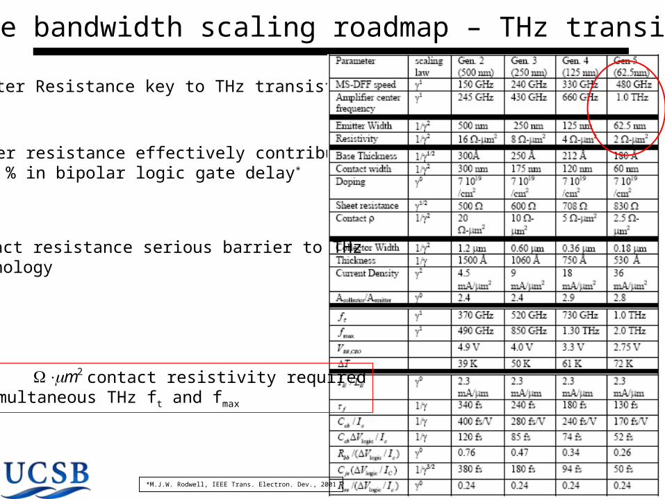
Device bandwidth scaling roadmap – THz transistor
Emitter Resistance key to THz transistor
Emitter resistance effectively contributes > 50 % in bipolar logic gate delay*
Contact resistance serious barrier to THztechnology
2 contact resistivity requiredfor simultaneous THz ft and fmax
2m
*M.J.W. Rodwell, IEEE Trans. Electron. Dev., 2001

2007 DRC
Device bandwidth scaling-FETs
Source contact resistance must scale to the inverse square of device scaling
Low source resistance means better NF in FETs*
f
fRRRgNF igsmi )(1min
P + substrate
barrier
sidewall
metal gate
gL
undopedsubstrate
wT
quantum well
gatedielectric
N+ regrowth N+ regrowth
source contact drain contactoxT
undopedsubstrate
S/DL
50 nm
Source resistance reduces gm and Id
A 22 nm III-V MOSFET with 5 mA/m Id
15 source resistance will reduceId by 10%
With 50 nm contact width this will require of 1
*T Takahashi ,IPRM 07
m
2mc
2007 DRC
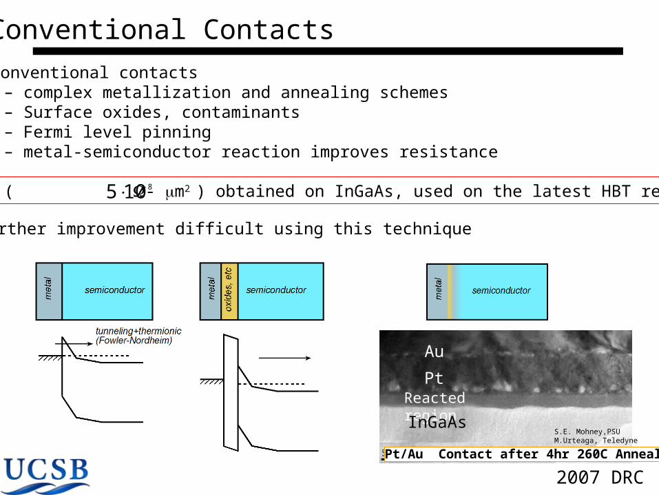
Conventional Contacts• Conventional contacts
– complex metallization and annealing schemes– Surface oxides, contaminants – Fermi level pinning– metal-semiconductor reaction improves resistance
Au
5 - m2 ( - m2 ) obtained on InGaAs, used on the latest HBT results
Further improvement difficult using this technique
Reacted regionPt
InGaAs
Pt/Au Contact after 4hr 260C Anneal
S.E. Mohney,PSUM.Urteaga, Teledyne
8105

2007 DRC
In-situ ErAs-InGaAs Contacts
• Epitaxial ErAs-InGaAs contact – Epitaxially formed, no surface defects, no fermi level pinning– In-situ, no surface oxides– thermodynamically stable– ErAs/InAs fermi level should be above conduction band
III Er As
Approximate Schottky barrier potential
D. O. Klenov, Appl. Phys. Lett., 2005
1J.D. Zimmerman et al., J. Vac. Sci. Technol. B, 2005
InAlAs/InGaAs
S.R. Bank, NAMBE , 2006
2007 DRC
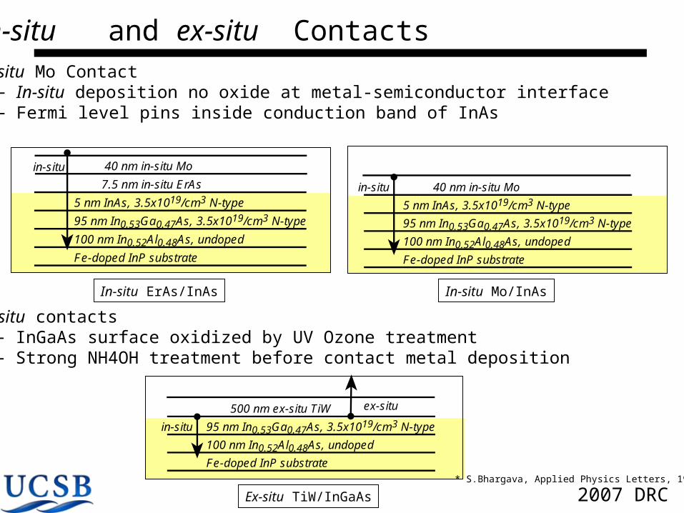
In-situ and ex-situ Contacts• In-situ Mo Contact
– In-situ deposition no oxide at metal-semiconductor interface– Fermi level pins inside conduction band of InAs
* S.Bhargava, Applied Physics Letters, 1997
Fe-doped InP substrate
100 nm In0.52Al0.48As, undoped
95 nm In0.53Ga0.47As, 3.5x10¹⁹/cm3 N-type
5 nm InAs, 3.5x10¹⁹/cm3 N-type
40 nm in-situ Mo
in-situ ErAs
7.5 nm in-situ ErAs
in-situ
Fe-doped InP substrate
100 nm In0.52Al0.48As, undoped
95 nm In0.53Ga0.47As, 3.5x10¹⁹/cm3 N-type
5 nm InAs, 3.5x10¹⁹/cm3 N-type
40 nm in-situ Mo in-situ
in-situ Mo
Fe-doped InP substrate
100 nm In0.52Al0.48As, undoped
95 nm In0.53Ga0.47As, 3.5x10¹⁹/cm3 N-type
500 nm ex-situ TiW
in-situ
ex-situ
ex-situ TiW
• Ex-situ contacts– InGaAs surface oxidized by UV Ozone treatment– Strong NH4OH treatment before contact metal deposition
In-situ ErAs/InAs In-situ Mo/InAs
Ex-situ TiW/InGaAs
2007 DRC
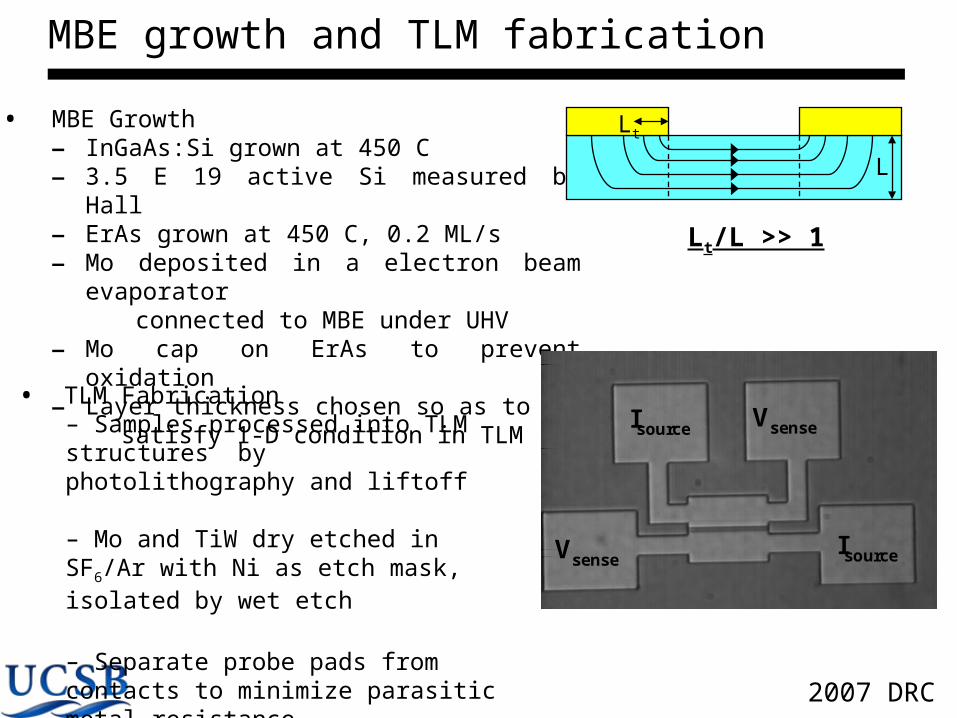
MBE growth and TLM fabrication
• MBE Growth– InGaAs:Si grown at 450 C – 3.5 E 19 active Si measured by Hall– ErAs grown at 450 C, 0.2 ML/s– Mo deposited in a electron beam evaporator connected to MBE under UHV– Mo cap on ErAs to prevent oxidation– Layer thickness chosen so as to satisfy 1-D condition in TLM
• TLM Fabrication– Samples processed into TLM structures by photolithography and liftoff
– Mo and TiW dry etched in SF6/Ar with Ni as etch mask, isolated by wet etch
– Separate probe pads from contacts to minimize parasitic metal resistance
Isource
Isource
Vsense
Vsense
Isource
Isource
Vsense
Vsense
Isource
Isource
Vsense
Vsense
Isource
Isource
Vsense
Vsense
(a)
(b)
Isource
Isource
Vsense
Vsense
Isource
Isource
Vsense
Vsense
Isource
Isource
Vsense
Vsense
Isource
Isource
Vsense
Vsense
(a)
(b)
L
Lt
Lt/L >> 1

2007 DRC
Contact Resistance
Contact Lt (nm)
ErAs/InAs 1.5 300
Mo/InAs 0.5 175
TiW/InGaAs 0.7 190
)( 2mc
Isource
Isource
Vsense
Vsense
Isource
Isource
Vsense
Vsense
Isource
Isource
Vsense
Vsense
Isource
Isource
Vsense
Vsense
(a)
(b)
Isource
Isource
Vsense
Vsense
Isource
Isource
Vsense
Vsense
Isource
Isource
Vsense
Vsense
Isource
Isource
Vsense
Vsense
(a)
(b)
0
0.5
1
1.5
2
2.5
3
3.5
4
0 1 2 3 4 5 6Pad Spacing (m)
Re
sist
ance
(
)
TiW/InGaAs
ErAs/InAs
Mo/InAs
0
5
10
15
20
0 5 10 15 20 25 30
Re
sis
tan
ce (
Pad Spacing (m)
• Resistance measured by 4155 C parameter analyzer• Pad spacing verified by SEM image• Smallest gap, contact resistance 60 % of total resistance
• 15-18 Ohm sheet resistance for all three contacts
W
RR SCC
22
282 1011 cmm
2007 DRC
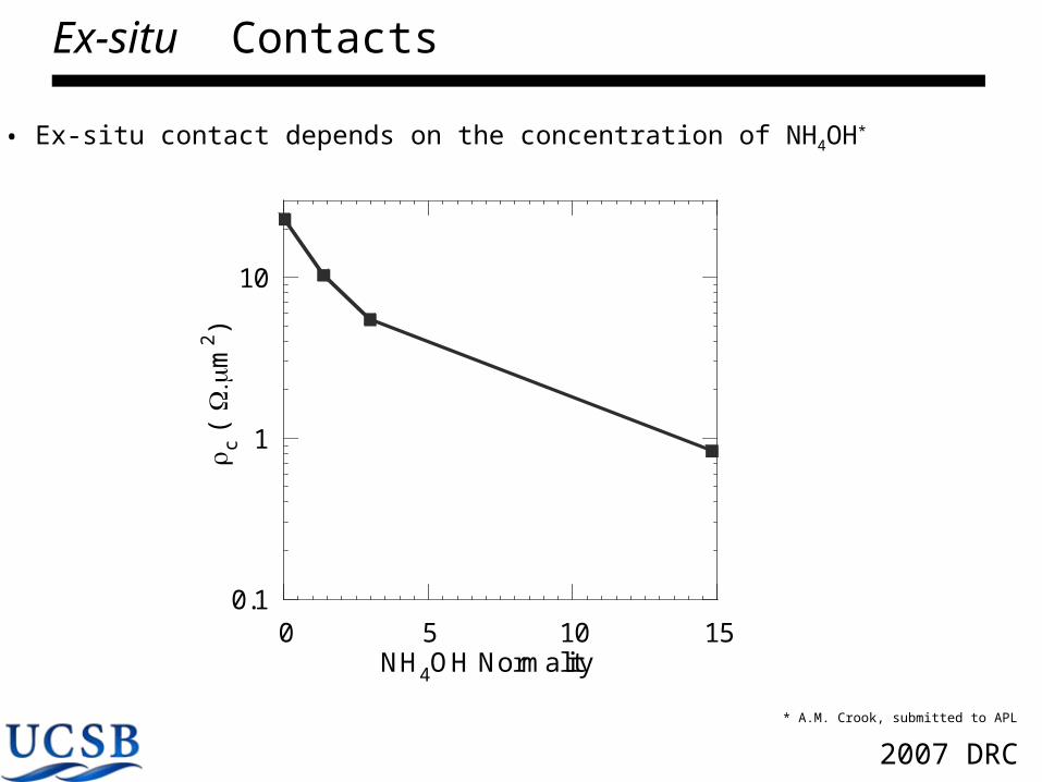
Ex-situ Contacts
0.1
1
10
0 5 10 15
c (
m
2)
NH4OH Normality
• Ex-situ contact depends on the concentration of NH4OH*
* A.M. Crook, submitted to APL

2007 DRC
Thermal Stability
0.1
1
10
100
0 100 200 300 400 500
Temperature (C)
Sp
eci
fic
Co
nta
ct
Res
isti
vity
(
m
2)
As DepositedErAs/InAs
TiW/InGaAs
Mo/InAs
• Contacts annealed under N2 flow at different temperatures• Contacts stays Ohmic after anneal • In-situ Mo/InAs, ex-situ TiW/InGaAs contact resistivity < 1 -m2 after anneal
• ErAs/InAs contact resistivity increases with anneal
• The increase could be due to lateral oxidation of ErAs

2007 DRC
Thermal Stability
0 50 100 150 200 250 300 350 400
Inte
nsi
ty (
arb
. un
its
)
Etching Time (sec)
Ni
Ti
Au
Mo
In
Ga
• SIMS depth profiling shows that Mo and TiW act as diffusion barrier to Ti and Au
SIMS profile of contacts annealed at 400 C
2007 DRC
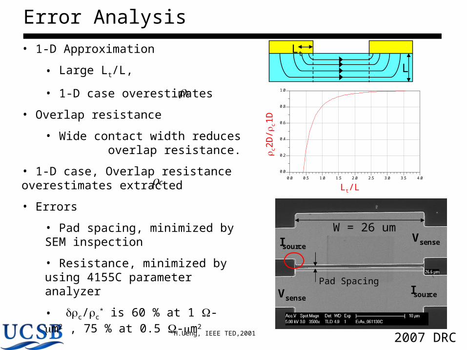
Error Analysis
• 1-D Approximation
• Large Lt/L,
• 1-D case overestimates
• Overlap resistance
• Wide contact width reduces overlap resistance.
• 1-D case, Overlap resistance overestimates extracted
• Errors
• Pad spacing, minimized by SEM inspection
• Resistance, minimized by using 4155C parameter analyzer
• c/c* is 60 % at 1 -m2 , 75 % at
0.5 -m2
c
L
Lt
Isource
Isource
Vsense
Vsense
Isource
Isource
Vsense
Vsense
Isource
Isource
Vsense
Vsense
Isource
Isource
Vsense
Vsense
(a)
(b)
Isource
Isource
Vsense
Vsense
Isource
Isource
Vsense
Vsense
Isource
Isource
Vsense
Vsense
Isource
Isource
Vsense
Vsense
(a)
(b)
W = 26 um
Pad Spacing
0.5 1.0 1.5 2.0 2.5 3.0 3.50.0 4.0
0.2
0.4
0.6
0.8
0.0
1.0
156.25*(V1-.032)
.000
256*
cont
act/(
(V1-
.032
)*(V
1-.0
32))
cLt/L
c2D
/c1
D
*H.Ueng, IEEE TED,2001
2007 DRC
Integration into Device Processing
barrier
well
r
barrier
well
r
barrier
well
r
barrier
well
r
barrier
well
r
(starting material) nonselective regrowth planarize etch strip resist
• Source Contact in FETs
• HBT emitter contact*
InGaAs/InP emitterInGaAs BaseInP Collector
SI substrate
Ti/W or Mo
Sub-Collector
InGaAs/InP emitterInGaAs BaseInP Collector
SI substrate
Ti/W
Sub-Collector
InGaAs BaseInP Collector
SI substrate
Ti/W
Sub-Collector
Blanket metal depostion Dry etch Emitter metal Dry + Wet etch Emitter
*E.Lind, Late News,DRC 2007

2007 DRC
Conclusion
• Ultra Low Ohmic contacts to InGaAs/InP with c < 1 -m2
• Contacts realized by both in-situ and ex-situ
• In-situ Mo/InAs and ex-situ TiW/InGaAs c < 1 -m2 even after 500 C anneal
• In-situ ErAs/InAs contacts c =1.5 -m2, increases gradually with anneal
This work was supported by Office of Naval Research (ONR) Ultra Low ResistanceContacts program and a grant by Swedish Research Council