Embed Size (px)
Citation preview

18-740: Computer Architecture
Recitation 2:
Rethinking Memory System Design
Prof. Onur Mutlu
Carnegie Mellon University
Fall 2015
September 8, 2015
Agenda
Why Do Research in Computer Architecture?
Project Proposal, Timeline, Topics
Review Assignments for Next Week
Rethinking Memory System Design
2

An Enabler: Moore’s Law
3
Moore, “Cramming more components onto integrated circuits,”Electronics Magazine, 1965. Component counts double every other year
Image source: Intel

4
Number of transistors on an integrated circuit doubles ~ every two years
Image source: Wikipedia
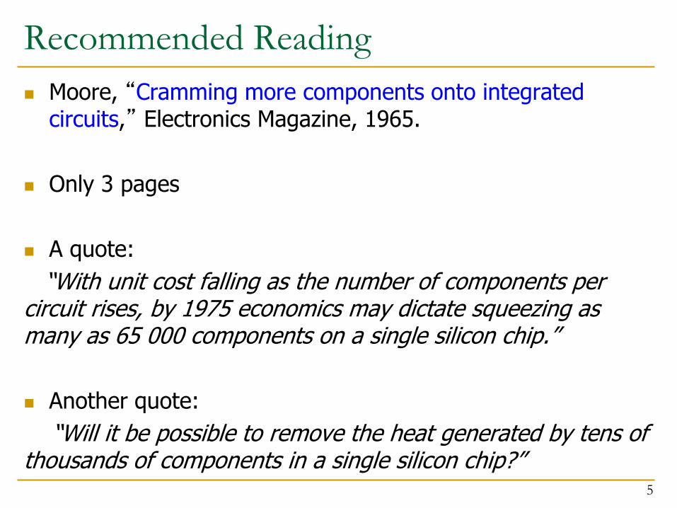
Recommended Reading
Moore, “Cramming more components onto integrated circuits,” Electronics Magazine, 1965.
Only 3 pages
A quote:
“With unit cost falling as the number of components per circuit rises, by 1975 economics may dictate squeezing as many as 65 000 components on a single silicon chip.”
Another quote:
“Will it be possible to remove the heat generated by tens of thousands of components in a single silicon chip?”
5

When Moore’s Law Ends …
All good things come to an end
How you architect systems will be even more important
When technology scaling ends or becomes more difficult
Every new beginning is another beginning’s end
Even if there is a replacement scalable technology, it will require new architectures to take advantage of it
6

Why Do Computer Architecture Research?
Enable better systems: make computers faster, cheaper, smaller, more reliable, …
By exploiting advances and changes in underlying technology/circuits
Enable new applications
Life-like 3D visualization 20 years ago?
Virtual reality?
Personalized genomics? Personalized medicine?
Enable better solutions to problems Software innovation is built into trends and changes in computer architecture
> 50% performance improvement per year has enabled this innovation
Overcome the challenges 7

Computer Architecture Today (I)
Today is a very exciting time to study computer architecture
Industry is in a large paradigm shift (to multi-core and beyond) – many different potential system designs possible
Many difficult problems motivating and caused by the shift
Power/energy constraints multi-core?
Complexity of design multi-core?
Difficulties in technology scaling new technologies?
Memory wall/gap
Reliability wall/issues
Programmability wall/problem
Huge hunger for data and new data-intensive applications
No clear, definitive answers to these problems8
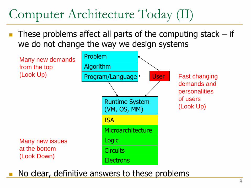
Computer Architecture Today (II)
These problems affect all parts of the computing stack – if we do not change the way we design systems
No clear, definitive answers to these problems9
Microarchitecture
ISA
Program/Language
Algorithm
Problem
Runtime System(VM, OS, MM)
User
Logic
Circuits
Electrons
Many new demands
from the top
(Look Up)
Many new issues
at the bottom
(Look Down)
Fast changing
demands and
personalities
of users
(Look Up)

Computer Architecture Today (III)
Computing landscape is very different from 10-20 years ago
Both UP (software and humanity trends) and DOWN (technologies and their issues), FORWARD and BACKWARD, and the resulting requirements and constraints
10
General Purpose GPUs
Heterogeneous
Processors and
Accelerators
Hybrid Main Memory
Persistent Memory/Storage
Every component and its
interfaces, as well as
entire system designs
are being re-examined

Computer Architecture Today (IV)
You can revolutionize the way computers are built, if you understand both the hardware and the software (and change each accordingly)
You can invent new paradigms for computation, communication, and storage
Recommended book: Thomas Kuhn, “The Structure of Scientific Revolutions” (1962)
Pre-paradigm science: no clear consensus in the field
Normal science: dominant theory used to explain/improve things (business as usual); exceptions considered anomalies
Revolutionary science: underlying assumptions re-examined
11

Computer Architecture Today (IV)
You can revolutionize the way computers are built, if you understand both the hardware and the software (and change each accordingly)
You can invent new paradigms for computation, communication, and storage
Recommended book: Thomas Kuhn, “The Structure of Scientific Revolutions” (1962)
Pre-paradigm science: no clear consensus in the field
Normal science: dominant theory used to explain/improve things (business as usual); exceptions considered anomalies
Revolutionary science: underlying assumptions re-examined
12

Agenda
Why Do Research in Computer Architecture?
Project Proposal, Timeline, Topics
Review Assignments for Next Week
Rethinking Memory System Design
13

Project Proposal and Topics
Research Project
Your chance to explore in depth a computer architecture topic that interests you
Perhaps even publish your innovation in a top computer architecture conference.
Start thinking about your project topic from now!
Interact with me and Nandita
Read the project topics handout well
Groups of 2-3 students (will finalize this later)
Proposal due: within ~3-4 weeks of first recitation session
Exact date will be announced
15

Project Timeline
Pre-Proposal: September 15
Proposal: September 25
Milestone 1 + Literature Review: October 13
Milestone 2: November 10
Report, Talk, Poster: TBD
http://www.ece.cmu.edu/~ece740/f15/doku.php?id=projects
16
Research Project
Goal: Develop (new) insight
Solve a problem in a new way or evaluate/analyze systems/ideas
Type 1:
Develop new ideas to solve an important problem
Rigorously evaluate the benefits and limitations of the ideas
Type 2:
Derive insight from rigorous analysis and understanding of existing systems or previously proposed ideas
Propose potential new solutions based on the new insight
The problem and ideas need to be concrete
Problem and goals need to be very clear
17

Research Proposal Outline: Type 1
The Problem: What is the problem you are trying to solve
Define very clearly. Explain why it is important.
Novelty: Why has previous research not solved this problem? What are its shortcomings?
Describe/cite all relevant works you know of and describe why these works are inadequate to solve the problem. This will be your literature survey.
Idea: What is your initial idea/insight? What new solution are you proposing to the problem? Why does it make sense? How does/could it solve the problem better?
Hypothesis: What is the main hypothesis you will test?
Methodology: How will you test the hypothesis/ideas? Describe what simulator or model you will use and what initial experiments you will do.
Plan: Describe the steps you will take. What will you accomplish by Milestone 1, 2, 3, and Final Report? Give 75%, 100%, 125% and moonshot goals.
All research projects can be (and should be) described in this fashion.
18

Research Proposal Outline: Type 2
The Problem: What is the problem/phenomenon you are trying to evaluate?
Define very clearly. Explain why it is important.
Novelty: How has previous research evaluated this? What are its shortcomings?
Describe/cite all relevant works you know of and describe why these works are inadequate to solve the problem. This will be your literature survey.
Evaluation method: How will you evaluate the phenomenon/idea? What experimental infrastructure will you design? How would that experimental infrastructure enable you to reliably evaluate the phenomenon/idea?
Hypotheses: What hypotheses will you test?
Methodology: What are your plans for evaluation? What experiments will you run? How will you do the data analysis?
Plan: Describe the steps you will take. What will you accomplish by Milestone 1, 2, 3, and Final Report? Give 75%, 100%, 125% and moonshot goals.
All research projects can be (and should be) described in this fashion.
19
Heilmeier’s Catechism (version 1)
What are you trying to do? Articulate your objectives using absolutely no jargon.
How is it done today, and what are the limits of current practice?
What's new in your approach and why do you think it will be successful?
Who cares?
If you're successful, what difference will it make?
What are the risks and the payoffs?
How much will it cost?
How long will it take?
What are the midterm and final "exams" to check for success?
20
Heilmeier’s Catechism (version 2)
What is the problem?
Why is it hard?
How is it solved today?
What is the new technical idea?
Why can we succeed now?
What is the impact if successful?
http://en.wikipedia.org/wiki/George_H._Heilmeier
21
Supplementary Readings on Research, Writing, Reviews
Hamming, “You and Your Research,” Bell Communications Research Colloquium Seminar, 7 March 1986.
http://www.cs.virginia.edu/~robins/YouAndYourResearch.html
Levin and Redell, “How (and how not) to write a good systems paper,” OSR 1983.
Smith, “The Task of the Referee,” IEEE Computer 1990.
Read this to get an idea of the publication process
SP Jones, “How to Write a Great Research Paper”
Fong, “How to Write a CS Research Paper: A Bibliography”22

Where to Get Project Topics/Ideas From
Project topics handout
Assigned readings
Recent conference proceedings
ISCA: http://www.informatik.uni-trier.de/~ley/db/conf/isca/
MICRO: http://www.informatik.uni-trier.de/~ley/db/conf/micro/
HPCA: http://www.informatik.uni-trier.de/~ley/db/conf/hpca/
ASPLOS: http://www.informatik.uni-trier.de/~ley/db/conf/asplos/
23

Agenda
Why Do Research in Computer Architecture?
Project Proposal, Timeline, Topics
Review Assignments for Next Week
Rethinking Memory System Design
24

Review Assignments for Next Week

Required Reviews
Due Tuesday Sep 15 @ 3pm
Enter your reviews on the review website
Start discussing ideas and thoughts on Piazza
26
Review Paper 1 (Required)
Junwhan Ahn, Sungpack Hong, Sungjoo Yoo, Onur Mutlu, and Kiyoung Choi,"A Scalable Processing-in-Memory Accelerator for Parallel Graph Processing"Proceedings of the 42nd International Symposium on Computer Architecture (ISCA), Portland, OR, June 2015. [Slides (pdf)] [Lightning Session Slides (pdf)]
Related reading (no review required): Junwhan Ahn, Sungjoo Yoo, Onur Mutlu, and Kiyoung Choi,
"PIM-Enabled Instructions: A Low-Overhead, Locality-Aware Processing-in-Memory Architecture"Proceedings of the 42nd International Symposium on Computer Architecture(ISCA), Portland, OR, June 2015. [Slides (pdf)] [Lightning Session Slides (pdf)]
27

Review Paper 2 (Required)
Stephen W. Keckler, William J. Dally, Brucek Khailany, Michael Garland, David Glasco,GPUs and the Future of Parallel Computing, IEEE Micro 2011.
Background reading (no review required)
Nickolls and Dally, The GPU Computing Era, IEEE Micro 2010.
Related reading (no review required)
Schulte et al., Achieving Exascale Capabilities through Heterogeneous Computing, IEEE Micro 2015.
http://dx.doi.org/10.1109/MM.2015.71
28

Review Paper 3 (Required)
Jeffrey D. Ullman, Experiments as Research Validation: Have We Gone Too Far?, CACM 2015.
http://cacm.acm.org/magazines/2015/9/191183-experiments-as-research-validation/fulltext
Related reading (no review required):
Michael Mitzenmacher, Theory Without Experiments: Have We Gone Too Far?, CACM 2015.
http://cacm.acm.org/magazines/2015/9/191184-theory-without-experiments/fulltext
29

Review Paper 4 (Required)
Nandita Vijaykumar, Gennady Pekhimenko, Adwait Jog, Abhishek Bhowmick, Rachata Ausavarungnirun, Chita Das, Mahmut Kandemir, Todd C. Mowry, and Onur Mutlu,"A Case for Core-Assisted Bottleneck Acceleration in GPUs: Enabling Flexible Data Compression with Assist Warps"Proceedings of the 42nd International Symposium on Computer Architecture (ISCA), Portland, OR, June 2015. [Slides (pptx) (pdf)] [Lightning Session Slides (pptx) (pdf)]
30
Review Paper 5 (Optional)
Yu Cai, Yixin Luo, Saugata Ghose, Erich F. Haratsch, Ken Mai, and Onur Mutlu,"Read Disturb Errors in MLC NAND Flash Memory: Characterization and Mitigation"Proceedings of the 45th Annual IEEE/IFIP International Conference on Dependable Systems and Networks (DSN), Rio de Janeiro, Brazil, June 2015. [Slides (pptx) (pdf)]
31

Agenda
Why Do Research in Computer Architecture?
Project Proposal, Timeline, Topics
Review Assignments for Next Week
Rethinking Memory System Design
32

Rethinking Memory System Design
(for Data-Intensive Computing)
Prof. Onur Mutlu
18-740 Recitation 2
September 8, 2015

The Main Memory System
Main memory is a critical component of all computing systems: server, mobile, embedded, desktop, sensor
Main memory system must scale (in size, technology, efficiency, cost, and management algorithms) to maintain performance growth and technology scaling benefits
34
Processor
and cachesMain Memory Storage (SSD/HDD)
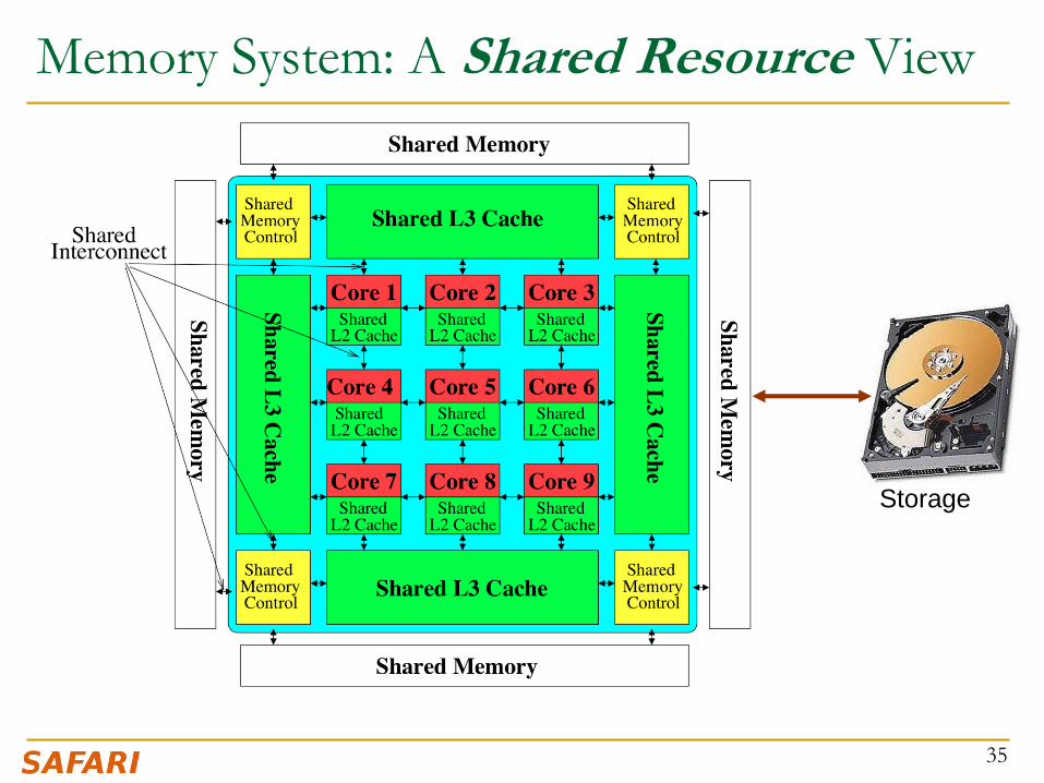
Memory System: A Shared Resource View
35
Storage

State of the Main Memory System
Recent technology, architecture, and application trends
lead to new requirements
exacerbate old requirements
DRAM and memory controllers, as we know them today, are (will be) unlikely to satisfy all requirements
Some emerging non-volatile memory technologies (e.g., PCM) enable new opportunities: memory+storage merging
We need to rethink the main memory system
to fix DRAM issues and enable emerging technologies
to satisfy all requirements36

Agenda
Major Trends Affecting Main Memory
The Memory Scaling Problem and Solution Directions
New Memory Architectures
Enabling Emerging Technologies
How Can We Do Better?
Summary
37

Major Trends Affecting Main Memory (I)
Need for main memory capacity, bandwidth, QoS increasing
Main memory energy/power is a key system design concern
DRAM technology scaling is ending
38

Major Trends Affecting Main Memory (II)
Need for main memory capacity, bandwidth, QoS increasing
Multi-core: increasing number of cores/agents
Data-intensive applications: increasing demand/hunger for data
Consolidation: cloud computing, GPUs, mobile, heterogeneity
Main memory energy/power is a key system design concern
DRAM technology scaling is ending
39

Example: The Memory Capacity Gap
Memory capacity per core expected to drop by 30% every two years
Trends worse for memory bandwidth per core!40
Core count doubling ~ every 2 years
DRAM DIMM capacity doubling ~ every 3 years
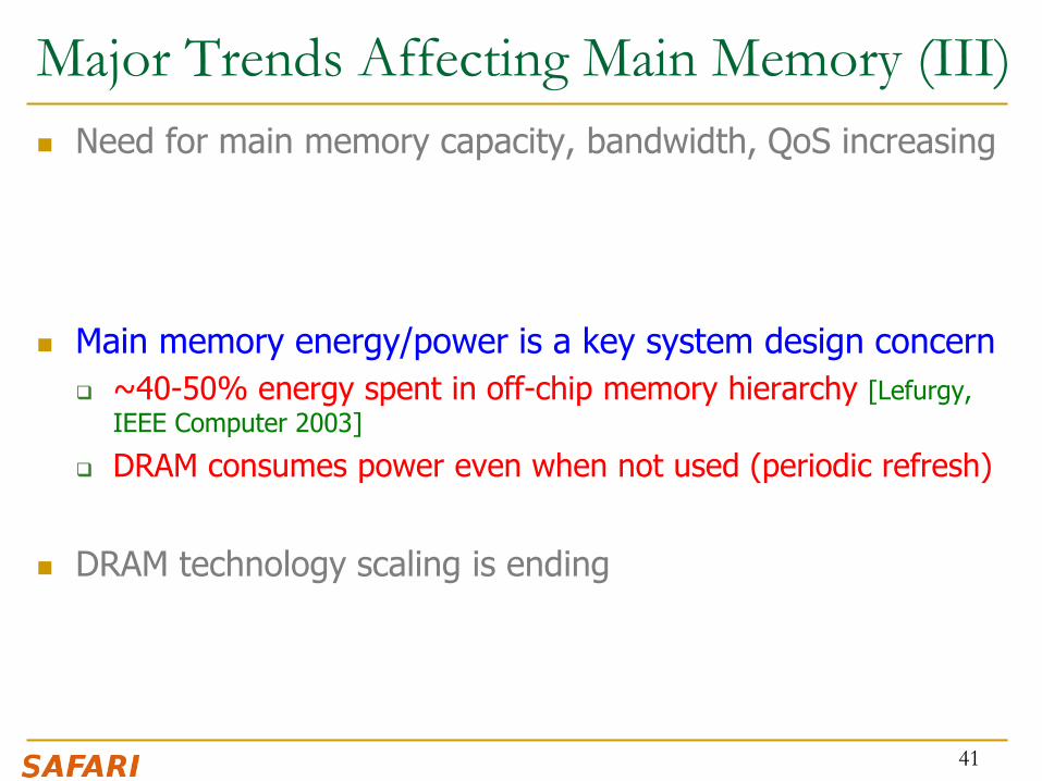
Major Trends Affecting Main Memory (III)
Need for main memory capacity, bandwidth, QoS increasing
Main memory energy/power is a key system design concern
~40-50% energy spent in off-chip memory hierarchy [Lefurgy,
IEEE Computer 2003]
DRAM consumes power even when not used (periodic refresh)
DRAM technology scaling is ending
41

Major Trends Affecting Main Memory (IV)
Need for main memory capacity, bandwidth, QoS increasing
Main memory energy/power is a key system design concern
DRAM technology scaling is ending
ITRS projects DRAM will not scale easily below X nm
Scaling has provided many benefits:
higher capacity (density), lower cost, lower energy
42

Agenda
Major Trends Affecting Main Memory
The Memory Scaling Problem and Solution Directions
New Memory Architectures
Enabling Emerging Technologies
How Can We Do Better?
Summary
43

The DRAM Scaling Problem
DRAM stores charge in a capacitor (charge-based memory)
Capacitor must be large enough for reliable sensing
Access transistor should be large enough for low leakage and high retention time
Scaling beyond 40-35nm (2013) is challenging [ITRS, 2009]
DRAM capacity, cost, and energy/power hard to scale
44

Row of Cells
RowRowRowRow
Wordline
VLOWVHIGHVictim Row
Victim Row
Hammered Row
Repeatedly opening and closing a row enough times within a refresh interval induces disturbance errors in adjacent rows in most real DRAM chips you can buy today
OpenedClosed
45
An Example of the DRAM Scaling Problem
Flipping Bits in Memory Without Accessing Them: An Experimental Study of DRAM Disturbance Errors, (Kim et al., ISCA 2014)

86%(37/43)
83%(45/54)
88%(28/32)
A company B company C company
Up to
1.0×10⁷
errors
Up to
2.7×10⁶
errors
Up to
3.3×10⁵
errors
46
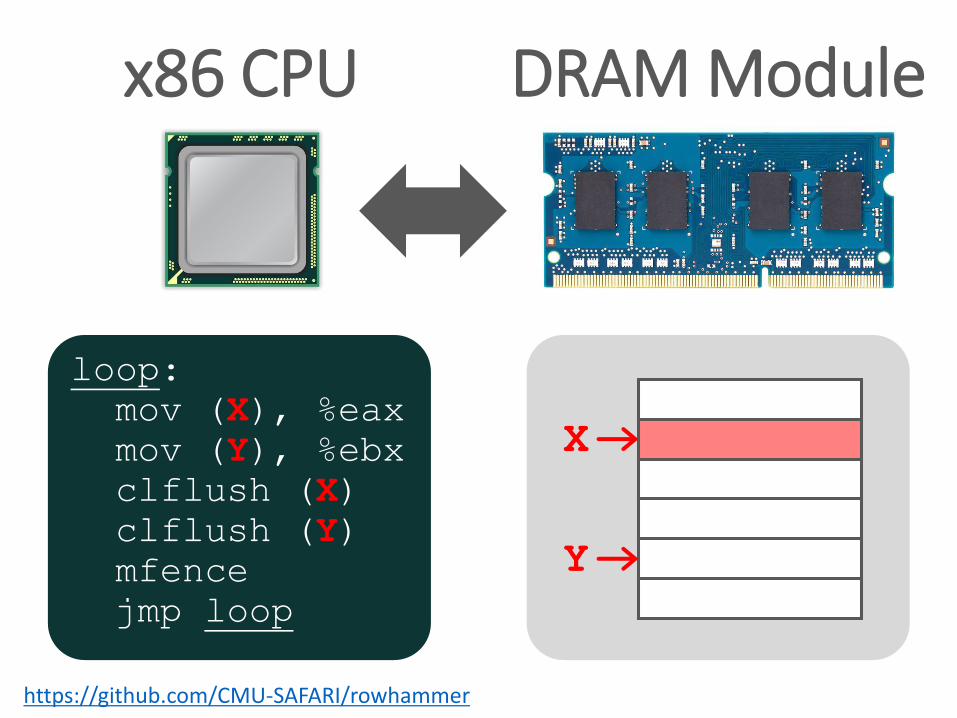
Most DRAM Modules Are at Risk
Flipping Bits in Memory Without Accessing Them: An Experimental Study of DRAM Disturbance Errors, (Kim et al., ISCA 2014)

DRAM Modulex86 CPU
Y
X
loop:
mov (X), %eax
mov (Y), %ebx
clflush (X)
clflush (Y)
mfence
jmp loop
https://github.com/CMU-SAFARI/rowhammer
DRAM Modulex86 CPU
loop:
mov (X), %eax
mov (Y), %ebx
clflush (X)
clflush (Y)
mfence
jmp loop
Y
X
https://github.com/CMU-SAFARI/rowhammer

DRAM Modulex86 CPU
loop:
mov (X), %eax
mov (Y), %ebx
clflush (X)
clflush (Y)
mfence
jmp loop
Y
X
https://github.com/CMU-SAFARI/rowhammer

DRAM Modulex86 CPU
loop:
mov (X), %eax
mov (Y), %ebx
clflush (X)
clflush (Y)
mfence
jmp loop
Y
X
https://github.com/CMU-SAFARI/rowhammer

• A real reliability & security issue
• In a more controlled environment, we can induce as many as ten million disturbance errors
CPU Architecture Errors Access-Rate
Intel Haswell (2013) 22.9K 12.3M/sec
Intel Ivy Bridge (2012) 20.7K 11.7M/sec
Intel Sandy Bridge (2011) 16.1K 11.6M/sec
AMD Piledriver (2012) 59 6.1M/sec
51Kim+, “Flipping Bits in Memory Without Accessing Them: An Experimental Study of DRAM Disturbance Errors,” ISCA 2014.
Observed Errors in Real Systems

52
All modules from 2012–2013 are vulnerable
FirstAppearance
Errors vs. Vintage

Experimental DRAM Testing Infrastructure
53
An Experimental Study of Data Retention Behavior in Modern DRAM Devices: Implications for Retention Time Profiling Mechanisms (Liu et al., ISCA 2013)
The Efficacy of Error Mitigation Techniques for DRAM Retention Failures: A Comparative Experimental Study(Khan et al., SIGMETRICS 2014)
Flipping Bits in Memory Without Accessing Them: An Experimental Study of DRAM Disturbance Errors (Kim et al., ISCA 2014)
Adaptive-Latency DRAM: Optimizing DRAM Timing for the Common-Case (Lee et al., HPCA 2015)
AVATAR: A Variable-Retention-Time (VRT) Aware Refresh for DRAM Systems (Qureshiet al., DSN 2015)

Experimental Infrastructure (DRAM)
54Kim+, “Flipping Bits in Memory Without Accessing Them: An Experimental Study of DRAM Disturbance Errors,” ISCA 2014.
TemperatureController
PC
HeaterFPGAs FPGAs

1. Most Modules Are at Risk
2. Errors vs. Vintage
3. Error = Charge Loss
4. Adjacency: Aggressor & Victim
5. Sensitivity Studies
6. Other Results in Paper
7. Solution Space
55
RowHammer Characterization Results
Flipping Bits in Memory Without Accessing Them: An Experimental Study of DRAM Disturbance Errors, (Kim et al., ISCA 2014)

One Can Take Over an Otherwise-Secure System
56
Exploiting the DRAM rowhammer bug to gain kernel privileges (Seaborn, 2015)
Flipping Bits in Memory Without Accessing Them: An Experimental Study of DRAM Disturbance Errors(Kim et al., ISCA 2014)

RowHammer Security Attack Example “Rowhammer” is a problem with some recent DRAM devices in which
repeatedly accessing a row of memory can cause bit flips in adjacent rows (Kim et al., ISCA 2014).
Flipping Bits in Memory Without Accessing Them: An Experimental Study of DRAM Disturbance Errors (Kim et al., ISCA 2014)
We tested a selection of laptops and found that a subset of them exhibited the problem.
We built two working privilege escalation exploits that use this effect.
Exploiting the DRAM rowhammer bug to gain kernel privileges (Seaborn, 2015)
One exploit uses rowhammer-induced bit flips to gain kernel privileges on x86-64 Linux when run as an unprivileged userland process.
When run on a machine vulnerable to the rowhammer problem, the process was able to induce bit flips in page table entries (PTEs).
It was able to use this to gain write access to its own page table, and hence gain read-write access to all of physical memory.
57Exploiting the DRAM rowhammer bug to gain kernel privileges (Seaborn, 2015)

Security Implications
58

Recap: The DRAM Scaling Problem
59

How Do We Solve The Problem?
Fix it: Make DRAM and controllers more intelligent
New interfaces, functions, architectures: system-DRAM codesign
Eliminate or minimize it: Replace or (more likely) augment DRAM with a different technology
New technologies and system-wide rethinking of memory & storage
Embrace it: Design heterogeneous memories (none of which are perfect) and map data intelligently across them
New models for data management and maybe usage
…
60
Solutions (to memory scaling) require software/hardware/device cooperation
Microarchitecture
ISA
Programs
Algorithms
Problems
Logic
Devices
Runtime System
(VM, OS, MM)
User

Solution 1: Fix DRAM
Overcome DRAM shortcomings with
System-DRAM co-design
Novel DRAM architectures, interface, functions
Better waste management (efficient utilization)
Key issues to tackle
Enable reliability at low cost
Reduce energy
Improve latency and bandwidth
Reduce waste (capacity, bandwidth, latency)
Enable computation close to data
61
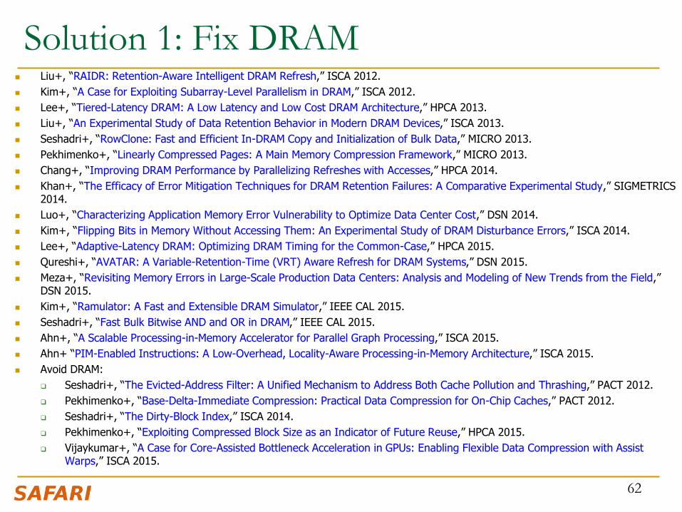
Solution 1: Fix DRAM Liu+, “RAIDR: Retention-Aware Intelligent DRAM Refresh,” ISCA 2012.
Kim+, “A Case for Exploiting Subarray-Level Parallelism in DRAM,” ISCA 2012.
Lee+, “Tiered-Latency DRAM: A Low Latency and Low Cost DRAM Architecture,” HPCA 2013.
Liu+, “An Experimental Study of Data Retention Behavior in Modern DRAM Devices,” ISCA 2013.
Seshadri+, “RowClone: Fast and Efficient In-DRAM Copy and Initialization of Bulk Data,” MICRO 2013.
Pekhimenko+, “Linearly Compressed Pages: A Main Memory Compression Framework,” MICRO 2013.
Chang+, “Improving DRAM Performance by Parallelizing Refreshes with Accesses,” HPCA 2014.
Khan+, “The Efficacy of Error Mitigation Techniques for DRAM Retention Failures: A Comparative Experimental Study,” SIGMETRICS 2014.
Luo+, “Characterizing Application Memory Error Vulnerability to Optimize Data Center Cost,” DSN 2014.
Kim+, “Flipping Bits in Memory Without Accessing Them: An Experimental Study of DRAM Disturbance Errors,” ISCA 2014.
Lee+, “Adaptive-Latency DRAM: Optimizing DRAM Timing for the Common-Case,” HPCA 2015.
Qureshi+, “AVATAR: A Variable-Retention-Time (VRT) Aware Refresh for DRAM Systems,” DSN 2015.
Meza+, “Revisiting Memory Errors in Large-Scale Production Data Centers: Analysis and Modeling of New Trends from the Field,” DSN 2015.
Kim+, “Ramulator: A Fast and Extensible DRAM Simulator,” IEEE CAL 2015.
Seshadri+, “Fast Bulk Bitwise AND and OR in DRAM,” IEEE CAL 2015.
Ahn+, “A Scalable Processing-in-Memory Accelerator for Parallel Graph Processing,” ISCA 2015.
Ahn+ “PIM-Enabled Instructions: A Low-Overhead, Locality-Aware Processing-in-Memory Architecture,” ISCA 2015.
Avoid DRAM:
Seshadri+, “The Evicted-Address Filter: A Unified Mechanism to Address Both Cache Pollution and Thrashing,” PACT 2012.
Pekhimenko+, “Base-Delta-Immediate Compression: Practical Data Compression for On-Chip Caches,” PACT 2012.
Seshadri+, “The Dirty-Block Index,” ISCA 2014.
Pekhimenko+, “Exploiting Compressed Block Size as an Indicator of Future Reuse,” HPCA 2015.
Vijaykumar+, “A Case for Core-Assisted Bottleneck Acceleration in GPUs: Enabling Flexible Data Compression with Assist Warps,” ISCA 2015.
62

Solution 2: Emerging Memory Technologies Some emerging resistive memory technologies seem more
scalable than DRAM (and they are non-volatile)
Example: Phase Change Memory
Expected to scale to 9nm (2022 [ITRS])
Expected to be denser than DRAM: can store multiple bits/cell
But, emerging technologies have shortcomings as well
Can they be enabled to replace/augment/surpass DRAM?
Lee+, “Architecting Phase Change Memory as a Scalable DRAM Alternative,” ISCA’09, CACM’10, Micro’10.
Meza+, “Enabling Efficient and Scalable Hybrid Memories,” IEEE Comp. Arch. Letters 2012.
Yoon, Meza+, “Row Buffer Locality Aware Caching Policies for Hybrid Memories,” ICCD 2012.
Kultursay+, “Evaluating STT-RAM as an Energy-Efficient Main Memory Alternative,” ISPASS 2013.
Meza+, “A Case for Efficient Hardware-Software Cooperative Management of Storage and Memory,” WEED 2013.
Lu+, “Loose Ordering Consistency for Persistent Memory,” ICCD 2014.
Zhao+, “FIRM: Fair and High-Performance Memory Control for Persistent Memory Systems,” MICRO 2014.
Yoon, Meza+, “Efficient Data Mapping and Buffering Techniques for Multi-Level Cell Phase-Change Memories,” ACM TACO 2014.
63

Solution 3: Hybrid Memory Systems
Meza+, “Enabling Efficient and Scalable Hybrid Memories,” IEEE Comp. Arch. Letters, 2012.
Yoon, Meza et al., “Row Buffer Locality Aware Caching Policies for Hybrid Memories,” ICCD 2012 Best Paper Award.
CPUDRAMCtrl
Fast, durableSmall,
leaky, volatile, high-cost
Large, non-volatile, low-costSlow, wears out, high active energy
PCM CtrlDRAM Technology X (e.g., PCM)
Hardware/software manage data allocation and movement to achieve the best of multiple technologies
App/Data A App/Data B App/Data C
Mem
ory
err
or
vuln
erab
ility
Vulnerable data
Tolerant data
Exploiting Memory Error Tolerance with Hybrid Memory Systems
Heterogeneous-Reliability Memory [DSN 2014]
Low-cost memoryReliable memory
Vulnerable data
Tolerant data
Vulnerable data
Tolerant data
• ECC protected• Well-tested chips
• NoECC or Parity• Less-tested chips
65
On Microsoft’s Web Search workloadReduces server hardware cost by 4.7 %Achieves single server availability target of 99.90 %

An Orthogonal Issue: Memory Interference
Main Memory
66
Core Core
Core Core
Cores’ interfere with each other when accessing shared main memory
Problem: Memory interference between cores is uncontrolled
unfairness, starvation, low performance
uncontrollable, unpredictable, vulnerable system
Solution: QoS-Aware Memory Systems
Hardware designed to provide a configurable fairness substrate
Application-aware memory scheduling, partitioning, throttling
Software designed to configure the resources to satisfy different QoS goals
QoS-aware memory systems can provide predictable performance and higher efficiency
An Orthogonal Issue: Memory Interference
Goal: Predictable Performance in Complex Systems
Heterogeneous agents: CPUs, GPUs, and HWAs
Main memory interference between CPUs, GPUs, HWAs
68
CPU CPU CPU CPU
Shared Cache
GPU
HWA HWA
DRAM and Hybrid Memory Controllers
DRAM and Hybrid Memories
How to allocate resources to heterogeneous agentsto mitigate interference and provide predictable performance?

Strong Memory Service Guarantees
Goal: Satisfy performance/SLA requirements in the presence of shared main memory, heterogeneous agents, and hybrid memory/storage
Approach:
Develop techniques/models to accurately estimate the performance loss of an application/agent in the presence of resource sharing
Develop mechanisms (hardware and software) to enable the resource partitioning/prioritization needed to achieve the required performance levels for all applications
All the while providing high system performance
Example work: Subramanian et al., “MISE: Providing Performance Predictability and Improving Fairness in Shared Main Memory Systems,” HPCA 2013.
69

Some Promising Directions
New memory architectures Rethinking DRAM and flash memory
A lot of hope in fixing DRAM
Enabling emerging NVM technologies Hybrid memory systems
Single-level memory and storage
A lot of hope in hybrid memory systems and single-level stores
System-level memory/storage QoS A lot of hope in designing a predictable system
70
We did not cover the remaining slides in
Recitation 2.
Agenda
Major Trends Affecting Main Memory
The Memory Scaling Problem and Solution Directions
New Memory Architectures
Enabling Emerging Technologies
How Can We Do Better?
Summary
72
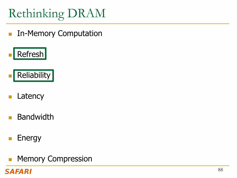
Rethinking DRAM
In-Memory Computation
Refresh
Reliability
Latency
Bandwidth
Energy
Memory Compression
73
Today’s Memory: Bulk Data Copy
Memory
MCL3L2L1CPU
1) High latency
2) High bandwidth utilization
3) Cache pollution
4) Unwanted data movement
741046ns, 3.6uJ (for 4KB page copy via DMA)
Future: RowClone (In-Memory Copy)
Memory
MCL3L2L1CPU
1) Low latency
2) Low bandwidth utilization
3) No cache pollution
4) No unwanted data movement
751046ns, 3.6uJ90ns, 0.04uJ

DRAM Subarray Operation (load one byte)
Row Buffer (8 Kbits)
Data Bus
8 bits
DRAM array
8 Kbits
Step 1: Activate row
Transfer
row
Step 2: Read
Transfer byte
onto bus

RowClone: In-DRAM Row Copy
Row Buffer (8 Kbits)
Data Bus
8 bits
DRAM array
8 Kbits
Step 1: Activate row A
Transfer
row
Step 2: Activate row B
Transfer
row0.01% area cost

Mem
ory
Chan
ne
l
Ch
ip I/
O
Bank Bank I/O
Subarray
Intra Subarray
Copy (2 ACTs)
Inter Bank Copy
(Pipelined
Internal RD/WR)
Inter Subarray Copy
(Use Inter-Bank Copy Twice)
Generalized RowClone
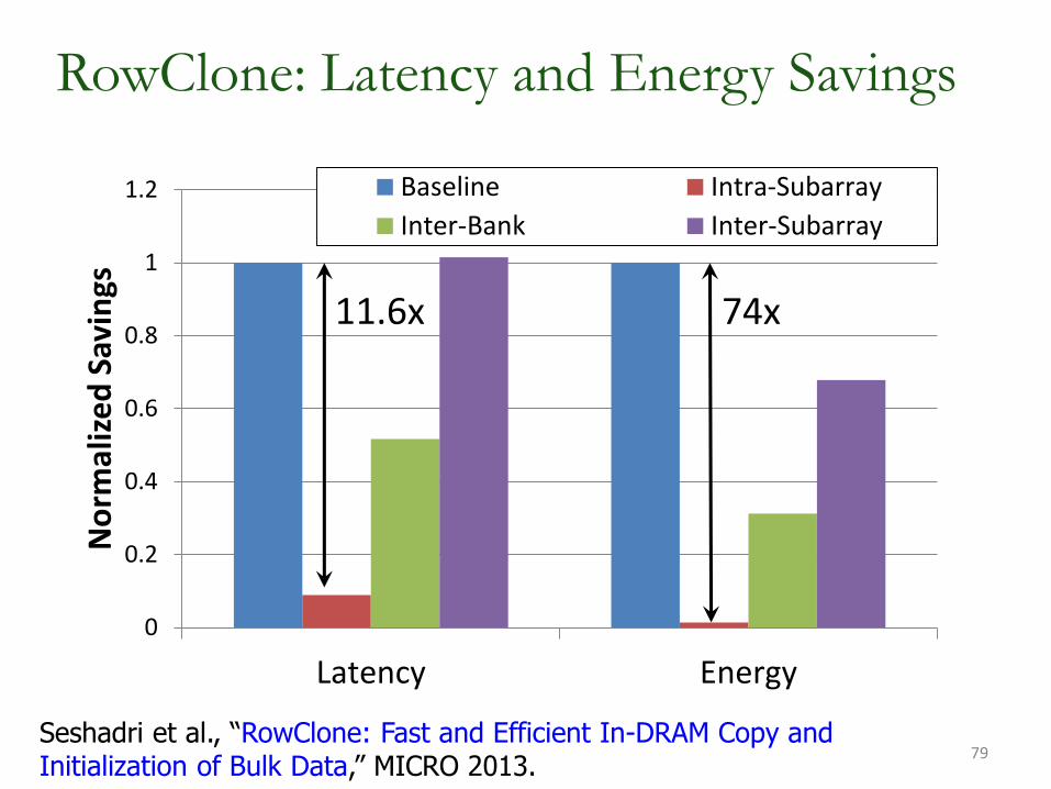
RowClone: Latency and Energy Savings
0
0.2
0.4
0.6
0.8
1
1.2
Latency Energy
No
rmal
ize
d S
avin
gs
Baseline Intra-Subarray
Inter-Bank Inter-Subarray
11.6x 74x
79Seshadri et al., “RowClone: Fast and Efficient In-DRAM Copy and Initialization of Bulk Data,” MICRO 2013.
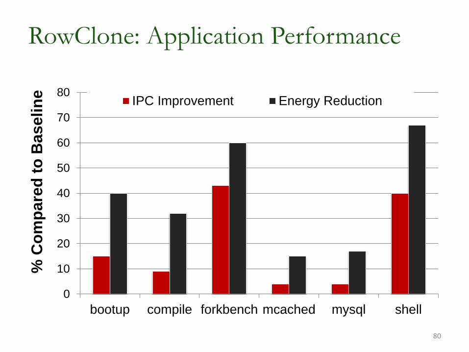
RowClone: Application Performance
80
0
10
20
30
40
50
60
70
80
bootup compile forkbench mcached mysql shell
% C
om
pare
d t
o B
aseli
ne
IPC Improvement Energy Reduction
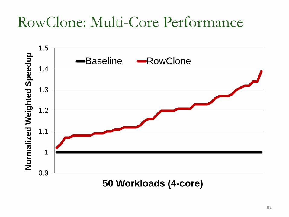
RowClone: Multi-Core Performance
81
0.9
1
1.1
1.2
1.3
1.4
1.5
No
rma
lize
d W
eig
hte
d S
pe
ed
up
50 Workloads (4-core)
Baseline RowClone

End-to-End System Design
82
DRAM (RowClone)
Microarchitecture
ISA
Operating System
ApplicationHow to communicate occurrences of bulk copy/initialization across layers?
How to maximize latency and energy savings?
How to ensure cache coherence?
How to handle data reuse?
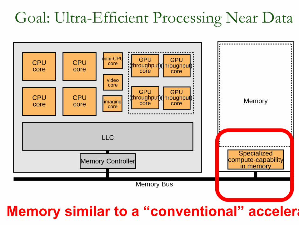
Goal: Ultra-Efficient Processing Near Data
CPUcore
CPUcore
CPUcore
CPUcore
mini-CPUcore
videocore
GPU(throughput)
core
GPU(throughput)
core
GPU(throughput)
core
GPU(throughput)
core
LLC
Memory Controller
Specializedcompute-capability
in memory
Memoryimagingcore
Memory Bus
Memory similar to a “conventional” accelerator
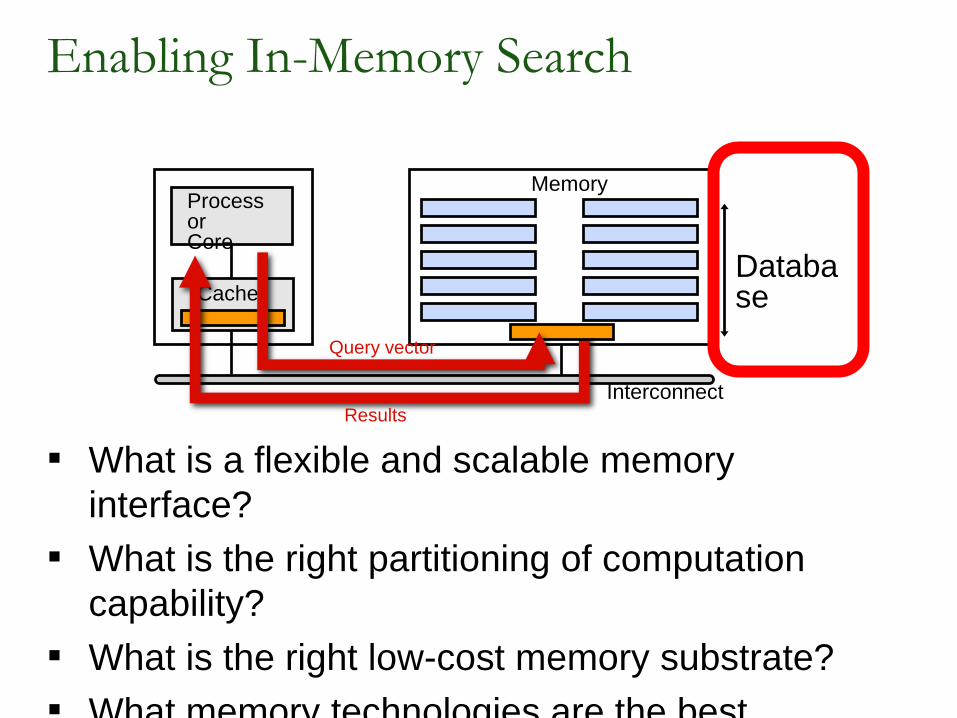
Enabling In-Memory Search
▪ What is a flexible and scalable memory
interface?
▪ What is the right partitioning of computation
capability?
▪ What is the right low-cost memory substrate?
▪ What memory technologies are the best
Cache
ProcessorCore
Interconnect
Memory
Database
Query vector
Results

Enabling In-Memory Computation
85
Virtual Memory Support
Cache Coherence
DRAM Support
RowClone(MICRO 2013)
Dirty-Block Index
(ISCA 2014)
Page Overlays (ISCA 2015)
In-DRAM Gather Scatter
In-DRAM Bitwise Operations
(IEEE CAL 2015)? ?
Non-contiguous Cache lines
Gathered Pages
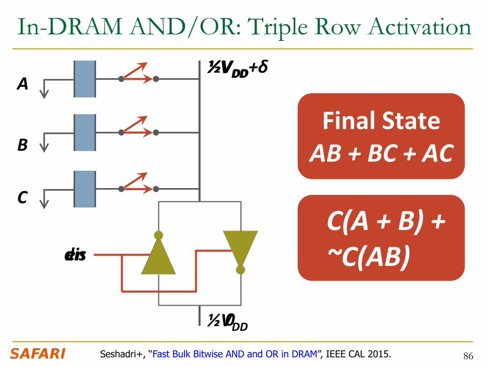
In-DRAM AND/OR: Triple Row Activation
86
½VDD
½VDD
dis
A
B
C
Final StateAB + BC + AC
½VDD+δ
C(A + B) + ~C(AB)en
0
VDD
Seshadri+, “Fast Bulk Bitwise AND and OR in DRAM”, IEEE CAL 2015.
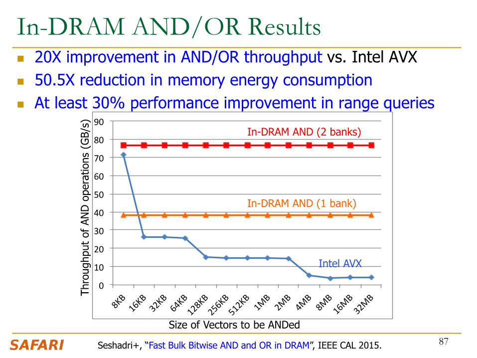
In-DRAM AND/OR Results 20X improvement in AND/OR throughput vs. Intel AVX
50.5X reduction in memory energy consumption
At least 30% performance improvement in range queries
87Seshadri+, “Fast Bulk Bitwise AND and OR in DRAM”, IEEE CAL 2015.
0
10
20
30
40
50
60
70
80
90
8KB
16KB
32KB
64KB
128KB
256KB
512KB
1MB
2MB
4MB
8MB
16MB
32MB
Size of Vectors to be ANDed
In-DRAM AND (2 banks)
In-DRAM AND (1 bank)
Intel AVX
Rethinking DRAM
In-Memory Computation
Refresh
Reliability
Latency
Bandwidth
Energy
Memory Compression
88

DRAM Refresh
DRAM capacitor charge leaks over time
The memory controller needs to refresh each row periodically to restore charge
Activate each row every N ms
Typical N = 64 ms
Downsides of refresh
-- Energy consumption: Each refresh consumes energy
-- Performance degradation: DRAM rank/bank unavailable while refreshed
-- QoS/predictability impact: (Long) pause times during refresh
-- Refresh rate limits DRAM capacity scaling
89

Refresh Overhead: Performance
90
8%
46%
Liu et al., “RAIDR: Retention-Aware Intelligent DRAM Refresh,” ISCA 2012.
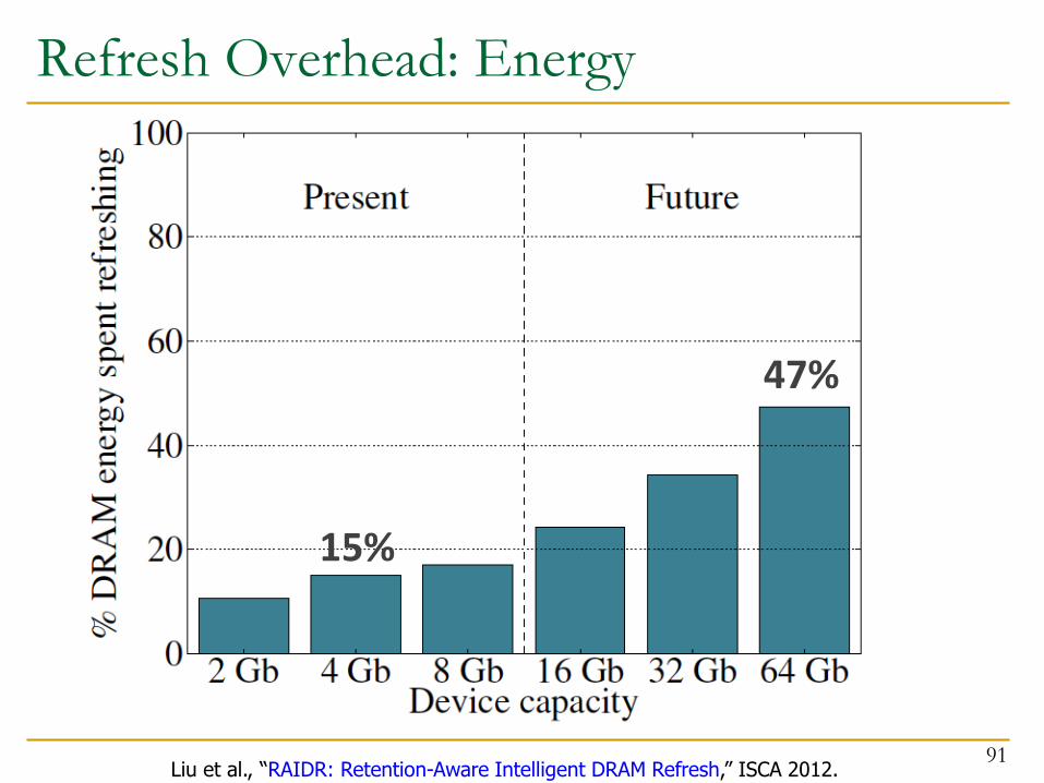
Refresh Overhead: Energy
91
15%
47%
Liu et al., “RAIDR: Retention-Aware Intelligent DRAM Refresh,” ISCA 2012.
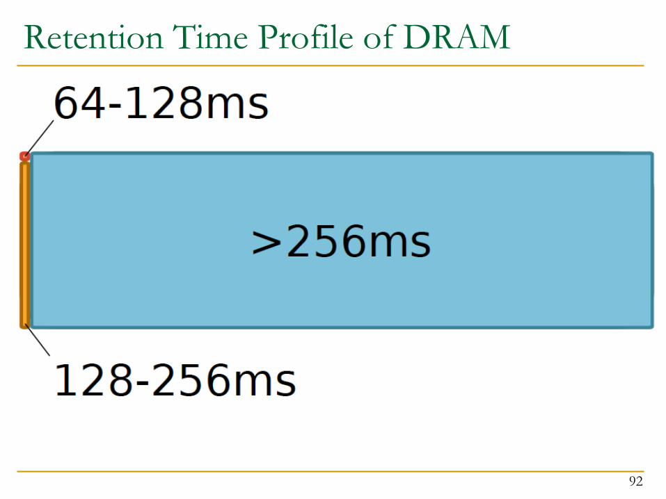
Retention Time Profile of DRAM
92

RAIDR: Eliminating Unnecessary Refreshes
Observation: Most DRAM rows can be refreshed much less often without losing data [Kim+, EDL’09][Liu+ ISCA’13]
Key idea: Refresh rows containing weak cells
more frequently, other rows less frequently
1. Profiling: Profile retention time of all rows
2. Binning: Store rows into bins by retention time in memory controller
Efficient storage with Bloom Filters (only 1.25KB for 32GB memory)
3. Refreshing: Memory controller refreshes rows in different bins at different rates
Results: 8-core, 32GB, SPEC, TPC-C, TPC-H
74.6% refresh reduction @ 1.25KB storage
~16%/20% DRAM dynamic/idle power reduction
~9% performance improvement
Benefits increase with DRAM capacity
93Liu et al., “RAIDR: Retention-Aware Intelligent DRAM Refresh,” ISCA 2012.

Going Forward (for DRAM and Flash)
How to find out weak memory cells/rows Liu+, “An Experimental Study of Data Retention Behavior in Modern DRAM Devices:
Implications for Retention Time Profiling Mechanisms”, ISCA 2013.
Khan+, “The Efficacy of Error Mitigation Techniques for DRAM Retention Failures: A Comparative Experimental Study,” SIGMETRICS 2014.
Low-cost system-level tolerance of memory errors Luo+, “Characterizing Application Memory Error Vulnerability to Optimize Data Center
Cost,” DSN 2014.
Cai+, “Error Analysis and Retention-Aware Error Management for NAND Flash Memory,” Intel Technology Journal 2013.
Cai+, “Neighbor-Cell Assisted Error Correction for MLC NAND Flash Memories,” SIGMETRICS 2014.
Tolerating cell-to-cell interference at the system level Kim+, “Flipping Bits in Memory Without Accessing Them: An Experimental Study of
DRAM Disturbance Errors,” ISCA 2014.
Cai+, “Program Interference in MLC NAND Flash Memory: Characterization, Modeling, and Mitigation,” ICCD 2013.
94
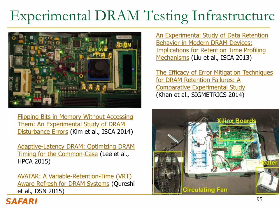
Experimental DRAM Testing Infrastructure
95
An Experimental Study of Data Retention Behavior in Modern DRAM Devices: Implications for Retention Time Profiling Mechanisms (Liu et al., ISCA 2013)
The Efficacy of Error Mitigation Techniques for DRAM Retention Failures: A Comparative Experimental Study(Khan et al., SIGMETRICS 2014)
Flipping Bits in Memory Without Accessing Them: An Experimental Study of DRAM Disturbance Errors (Kim et al., ISCA 2014)
Adaptive-Latency DRAM: Optimizing DRAM Timing for the Common-Case (Lee et al., HPCA 2015)
AVATAR: A Variable-Retention-Time (VRT) Aware Refresh for DRAM Systems (Qureshiet al., DSN 2015)
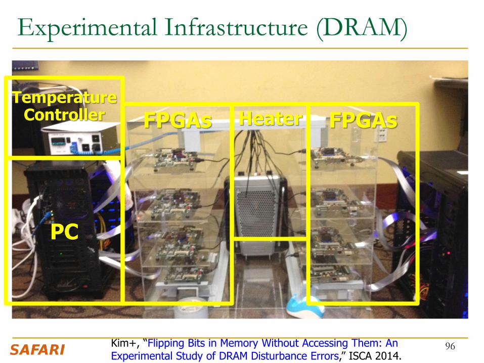
Experimental Infrastructure (DRAM)
96Kim+, “Flipping Bits in Memory Without Accessing Them: An Experimental Study of DRAM Disturbance Errors,” ISCA 2014.
TemperatureController
PC
HeaterFPGAs FPGAs

More Information [ISCA’13, SIGMETRICS’14]
97
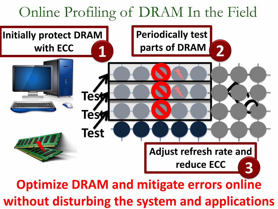
Optimize DRAM and mitigate errors online without disturbing the system and applications
Initially protect DRAM with ECC 1
Periodically testparts of DRAM 2
Test
Test
Test
Adjust refresh rate andreduce ECC 3
Online Profiling of DRAM In the Field

Rethinking DRAM
In-Memory Computation
Refresh
Reliability
Latency
Bandwidth
Energy
Memory Compression
99
100
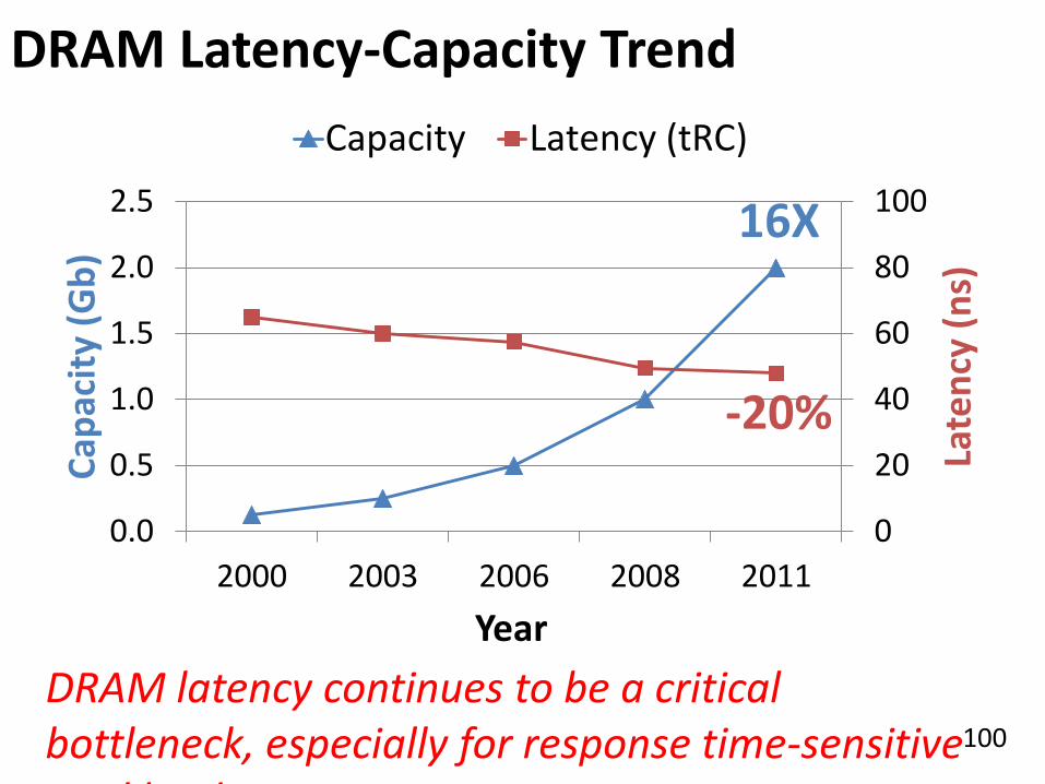
DRAM Latency-Capacity Trend
0
20
40
60
80
100
0.0
0.5
1.0
1.5
2.0
2.5
2000 2003 2006 2008 2011
Late
ncy
(n
s)
Cap
acit
y (G
b)
Year
Capacity Latency (tRC)
16X
-20%
DRAM latency continues to be a critical bottleneck, especially for response time-sensitive workloads

101
DRAM Latency = Subarray Latency + I/O Latency
What Causes the Long Latency?DRAM Chip
channel
cell array
I/O
DRAM Chip
channel
I/O
subarray
DRAM Latency = Subarray Latency + I/O Latency
DominantSu
bar
ray
I/O

102
Why is the Subarray So Slow?
Subarray
row
dec
od
er
sense amplifier
cap
acit
or
accesstransistor
wordline
bit
line
Cell
large sense amplifier
bit
line:
51
2 c
ells
cell
• Long bitline– Amortizes sense amplifier cost Small area
– Large bitline capacitance High latency & power
sen
se a
mp
lifie
r
row
dec
od
er

103
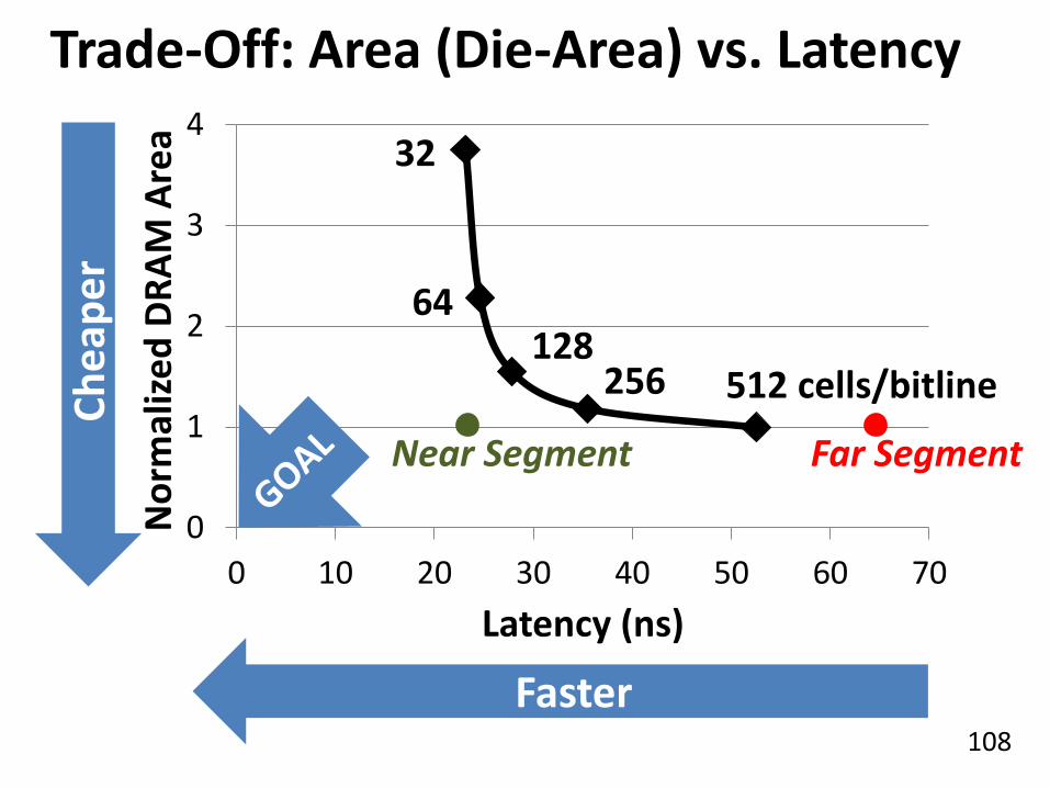
Trade-Off: Area (Die Size) vs. Latency
Faster
Smaller
Short BitlineLong Bitline
Trade-Off: Area vs. Latency

104
Trade-Off: Area (Die Size) vs. Latency
0
1
2
3
4
0 10 20 30 40 50 60 70
No
rmal
ize
d D
RA
M A
rea
Latency (ns)
64
32
128
256 512 cells/bitline
Commodity DRAM
Long Bitline
Ch
eap
er
Faster
Fancy DRAMShort Bitline

105
Short Bitline
Low Latency
Approximating the Best of Both Worlds
Long Bitline
Small Area
Long Bitline
Low Latency
Short BitlineOur Proposal
Small Area
Short Bitline Fast
Need Isolation
Add Isolation Transistors
High Latency
Large Area

106
Approximating the Best of Both Worlds
Low Latency
Our Proposal
Small Area Long BitlineSmall Area
Long Bitline
High Latency
Short Bitline
Low Latency
Short Bitline
Large Area
Tiered-Latency DRAM
Low Latency
Small area using long
bitline

107
0%
50%
100%
150%
0%
50%
100%
150%
Commodity DRAM vs. TL-DRAM [HPCA 2013] La
ten
cy
Po
we
r
–56%
+23%
–51%
+49%
• DRAM Latency (tRC) • DRAM Power
• DRAM Area Overhead~3%: mainly due to the isolation transistors
TL-DRAMCommodity
DRAM
Near Far Commodity DRAM
Near Far
TL-DRAM
(52.5ns)
108
Trade-Off: Area (Die-Area) vs. Latency
0
1
2
3
4
0 10 20 30 40 50 60 70
No
rmal
ize
d D
RA
M A
rea
Latency (ns)
64
32
128256 512 cells/bitline
Ch
eap
er
Faster
Near Segment Far Segment

109
Leveraging Tiered-Latency DRAM
• TL-DRAM is a substrate that can be leveraged by the hardware and/or software
• Many potential uses1. Use near segment as hardware-managed inclusive
cache to far segment
2. Use near segment as hardware-managed exclusivecache to far segment
3. Profile-based page mapping by operating system
4. Simply replace DRAM with TL-DRAM
Lee+, “Tiered-Latency DRAM: A Low Latency and Low Cost DRAM Architecture,” HPCA 2013.

110
0%
20%
40%
60%
80%
100%
120%
1 (1-ch) 2 (2-ch) 4 (4-ch)0%
20%
40%
60%
80%
100%
120%
1 (1-ch) 2 (2-ch) 4 (4-ch)
Performance & Power Consumption
11.5%
No
rmal
ize
d P
erf
orm
ance
Core-Count (Channel)N
orm
aliz
ed
Po
we
rCore-Count (Channel)
10.7%12.4%–23% –24% –26%
Using near segment as a cache improves performance and reduces power consumption
Lee+, “Tiered-Latency DRAM: A Low Latency and Low Cost DRAM Architecture,” HPCA 2013.

What Else Causes the Long DRAM Latency?
Conservative timing margins!
DRAM timing parameters are set to cover the worst case
Worst-case temperatures
85 degrees vs. common-case
to enable a wide range of operating conditions
Worst-case devices
DRAM cell with smallest charge across any acceptable device
to tolerate process variation at acceptable yield
This leads to large timing margins for the common case
111

Adaptive-Latency DRAM [HPCA 2015]
Idea: Optimize DRAM timing for the common case
Current temperature
Current DRAM module
Why would this reduce latency?
A DRAM cell can store much more charge in the common case (low temperature, strong cell) than in the worst case
More charge in a DRAM cell
Faster sensing, charge restoration, precharging
Faster access (read, write, refresh, …)
112Lee+, “Adaptive-Latency DRAM: Optimizing DRAM Timing for the Common-Case,” HPCA 2015.

113
AL-DRAM
• Key idea– Optimize DRAM timing parameters online
• Two components– DRAM manufacturer provides multiple sets of
reliable DRAM timing parameters at different temperatures for each DIMM
– System monitors DRAM temperature & uses appropriate DRAM timing parameters
reliable DRAM timing parameters
DRAM temperature
Lee+, “Adaptive-Latency DRAM: Optimizing DRAM Timing for the Common-Case,” HPCA 2015.

114
Latency Reduction Summary of 115 DIMMs
• Latency reduction for read & write (55°C)– Read Latency: 32.7%
– Write Latency: 55.1%
• Latency reduction for each timing parameter (55°C) – Sensing: 17.3%
– Restore: 37.3% (read), 54.8% (write)
– Precharge: 35.2%
Lee+, “Adaptive-Latency DRAM: Optimizing DRAM Timing for the Common-Case,” HPCA 2015.

115
AL-DRAM: Real System Evaluation
• System– CPU: AMD 4386 ( 8 Cores, 3.1GHz, 8MB LLC)
– DRAM: 4GByte DDR3-1600 (800Mhz Clock)
– OS: Linux
– Storage: 128GByte SSD
• Workload– 35 applications from SPEC, STREAM, Parsec,
Memcached, Apache, GUPS

116
0%5%
10%15%20%25%
sop
lex
mcf
milc
libq
lbm
gem
s
cop
y
s.cl
ust
er
gup
s
no
n-i
nte
nsi
ve
inte
nsi
ve
all-
wo
rklo
ads
Single Core Multi Core
0%5%
10%15%20%25%
sop
lex
mcf
milc
libq
lbm
gem
s
cop
y
s.cl
ust
er
gup
s
no
n-i
nte
nsi
ve
inte
nsi
ve
all-
wo
rklo
ads
Single Core Multi Core
1.4%
6.7%
0%5%
10%15%20%25%
sop
lex
mcf
milc
libq
lbm
gem
s
cop
y
s.cl
ust
er
gup
s
no
n-i
nte
nsi
ve
inte
nsi
ve
all-
wo
rklo
ads
Single Core Multi Core
5.0%
AL-DRAM: Single-Core Evaluation
AL-DRAM improves performance on a real system
Perf
orm
ance
Imp
rove
men
t AverageImprovement
all-
35
-wo
rklo
ad

117
0%5%
10%15%20%25%
sop
lex
mcf
milc
libq
lbm
gem
s
cop
y
s.cl
ust
er
gup
s
no
n-i
nte
nsi
ve
inte
nsi
ve
all-
wo
rklo
ads
Single Core Multi Core
0%5%
10%15%20%25%
sop
lex
mcf
milc
libq
lbm
gem
s
cop
y
s.cl
ust
er
gup
s
no
n-i
nte
nsi
ve
inte
nsi
ve
all-
wo
rklo
ads
Single Core Multi Core
0%5%
10%15%20%25%
sop
lex
mcf
milc
libq
lbm
gem
s
cop
y
s.cl
ust
er
gup
s
no
n-i
nte
nsi
ve
inte
nsi
ve
all-
wo
rklo
ads
Single Core Multi Core
14.0%
2.9%0%5%
10%15%20%25%
sop
lex
mcf
milc
libq
lbm
gem
s
cop
y
s.cl
ust
er
gup
s
no
n-i
nte
nsi
ve
inte
nsi
ve
all-
wo
rklo
ads
Single Core Multi Core
10.4%
AL-DRAM: Multi-Core Evaluation
AL-DRAM provides higher performance formulti-programmed & multi-threaded workloads
Perf
orm
ance
Imp
rove
men
t Average Improvement
all-
35
-wo
rklo
ad

Rethinking DRAM
In-Memory Computation
Refresh
Reliability
Latency
Bandwidth
Energy
Memory Compression
118

Agenda
Major Trends Affecting Main Memory
The Memory Scaling Problem and Solution Directions
New Memory Architectures
Enabling Emerging Technologies
How Can We Do Better?
Summary
119

Solution 2: Emerging Memory Technologies
Some emerging resistive memory technologies seem more scalable than DRAM (and they are non-volatile)
Example: Phase Change Memory
Data stored by changing phase of material
Data read by detecting material’s resistance
Expected to scale to 9nm (2022 [ITRS])
Prototyped at 20nm (Raoux+, IBM JRD 2008)
Expected to be denser than DRAM: can store multiple bits/cell
But, emerging technologies have (many) shortcomings
Can they be enabled to replace/augment/surpass DRAM?
120
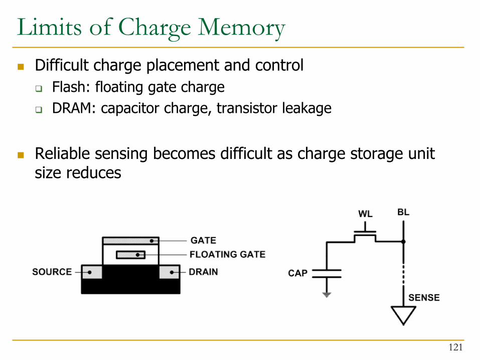
Limits of Charge Memory
Difficult charge placement and control
Flash: floating gate charge
DRAM: capacitor charge, transistor leakage
Reliable sensing becomes difficult as charge storage unit size reduces
121

Promising Resistive Memory Technologies
PCM
Inject current to change material phase
Resistance determined by phase
STT-MRAM
Inject current to change magnet polarity
Resistance determined by polarity
Memristors/RRAM/ReRAM
Inject current to change atomic structure
Resistance determined by atom distance
122

Phase Change Memory: Pros and Cons
Pros over DRAM
Better technology scaling (capacity and cost)
Non volatility
Low idle power (no refresh)
Cons
Higher latencies: ~4-15x DRAM (especially write)
Higher active energy: ~2-50x DRAM (especially write)
Lower endurance (a cell dies after ~108 writes)
Reliability issues (resistance drift)
Challenges in enabling PCM as DRAM replacement/helper:
Mitigate PCM shortcomings
Find the right way to place PCM in the system123

PCM-based Main Memory (I)
How should PCM-based (main) memory be organized?
Hybrid PCM+DRAM [Qureshi+ ISCA’09, Dhiman+ DAC’09]:
How to partition/migrate data between PCM and DRAM
124
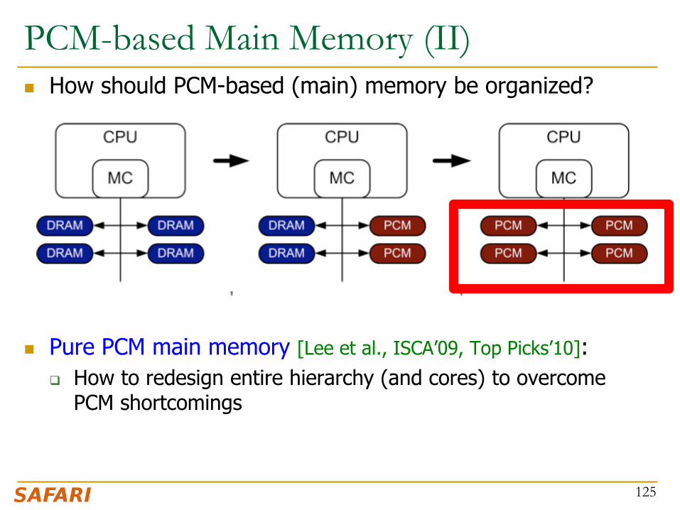
PCM-based Main Memory (II)
How should PCM-based (main) memory be organized?
Pure PCM main memory [Lee et al., ISCA’09, Top Picks’10]:
How to redesign entire hierarchy (and cores) to overcome PCM shortcomings
125
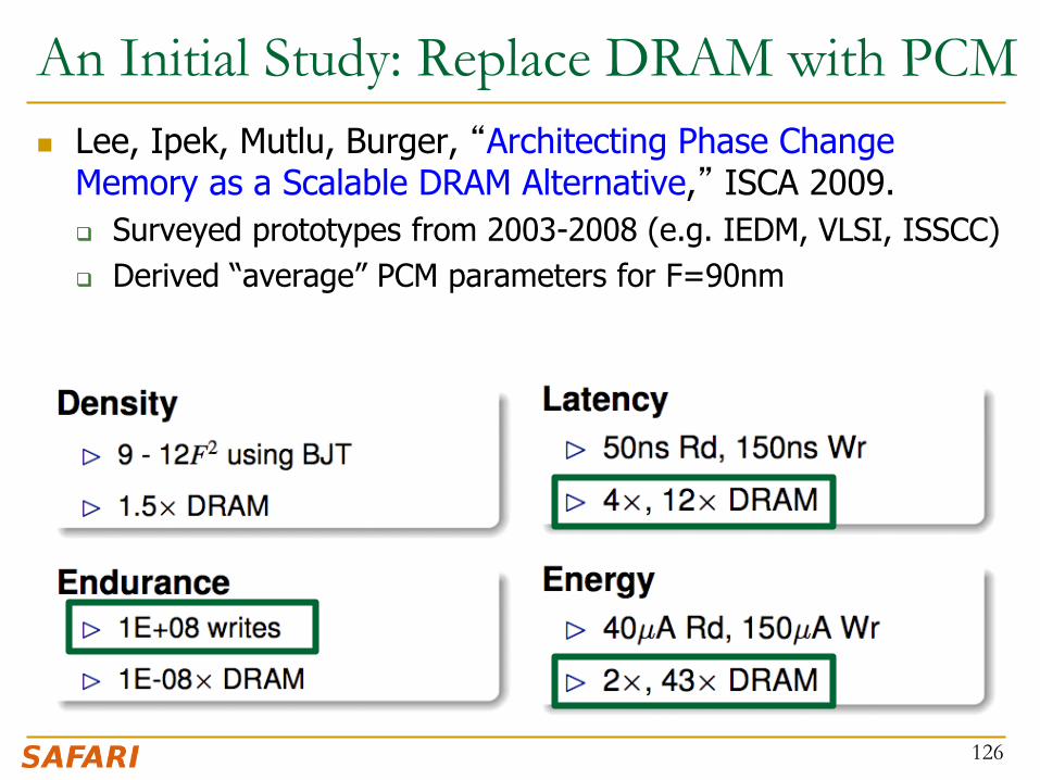
An Initial Study: Replace DRAM with PCM
Lee, Ipek, Mutlu, Burger, “Architecting Phase Change Memory as a Scalable DRAM Alternative,” ISCA 2009.
Surveyed prototypes from 2003-2008 (e.g. IEDM, VLSI, ISSCC)
Derived “average” PCM parameters for F=90nm
126
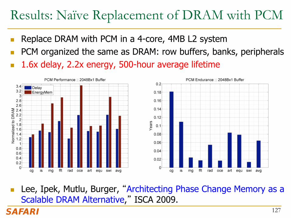
Results: Naïve Replacement of DRAM with PCM
Replace DRAM with PCM in a 4-core, 4MB L2 system
PCM organized the same as DRAM: row buffers, banks, peripherals
1.6x delay, 2.2x energy, 500-hour average lifetime
Lee, Ipek, Mutlu, Burger, “Architecting Phase Change Memory as a Scalable DRAM Alternative,” ISCA 2009.
127

Results: Architected PCM as Main Memory
1.2x delay, 1.0x energy, 5.6-year average lifetime
Scaling improves energy, endurance, density
Caveat 1: Worst-case lifetime is much shorter (no guarantees)
Caveat 2: Intensive applications see large performance and energy hits
Caveat 3: Optimistic PCM parameters?128
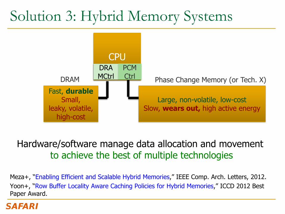
Solution 3: Hybrid Memory Systems
Meza+, “Enabling Efficient and Scalable Hybrid Memories,” IEEE Comp. Arch. Letters, 2012.
Yoon+, “Row Buffer Locality Aware Caching Policies for Hybrid Memories,” ICCD 2012 Best Paper Award.
CPUDRAMCtrl
Fast, durableSmall,
leaky, volatile, high-cost
Large, non-volatile, low-costSlow, wears out, high active energy
PCM CtrlDRAM Phase Change Memory (or Tech. X)
Hardware/software manage data allocation and movement to achieve the best of multiple technologies

0
0.2
0.4
0.6
0.8
1
1.2
1.4
1.6
1.8
2
Weighted Speedup Max. Slowdown Perf. per Watt
Normalized Metric
16GB PCM RBLA-Dyn 16GB DRAM
0
0.2
0.4
0.6
0.8
1
1.2
1.4
1.6
1.8
2
No
rma
lize
d W
eig
hte
d S
pee
du
p
0
0.2
0.4
0.6
0.8
1
1.2
No
rma
lize
d M
ax
. S
low
do
wn
Hybrid vs. All-PCM/DRAM [ICCD’12]
31% better performance than all PCM, within 29% of all DRAM performance
31%
29%
Yoon+, “Row Buffer Locality-Aware Data Placement in Hybrid Memories,” ICCD 2012 Best Paper Award.
STT-MRAM as Main Memory
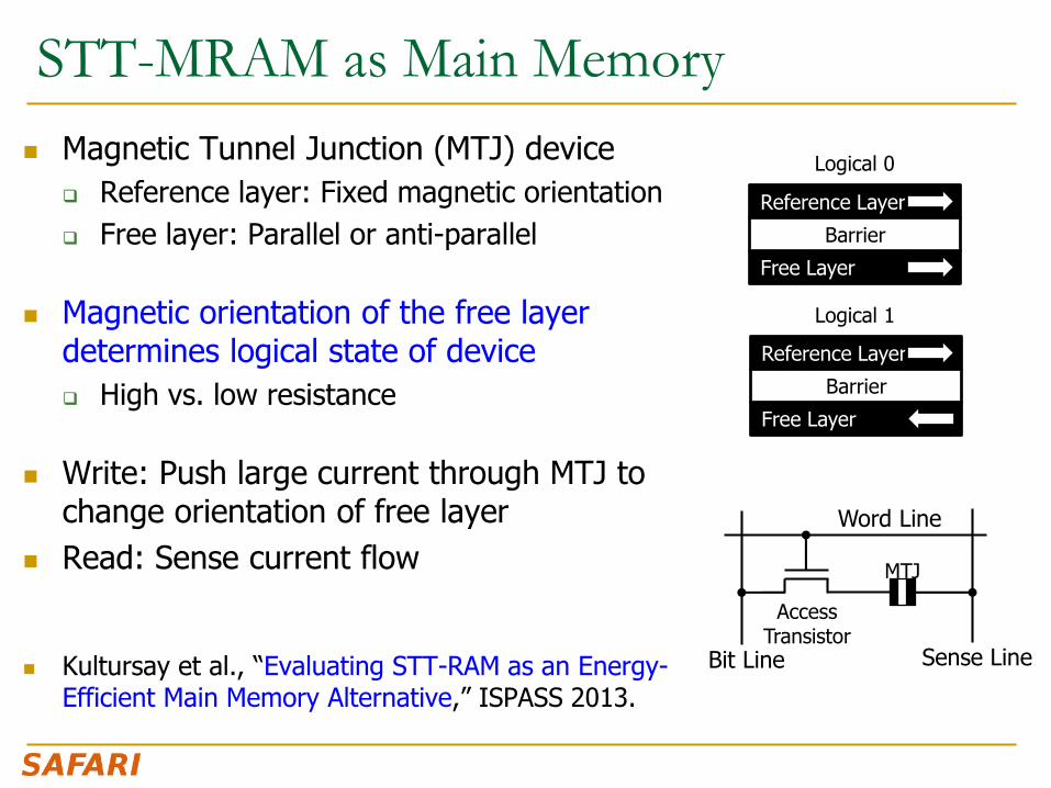
Magnetic Tunnel Junction (MTJ) device
Reference layer: Fixed magnetic orientation
Free layer: Parallel or anti-parallel
Magnetic orientation of the free layer determines logical state of device
High vs. low resistance
Write: Push large current through MTJ to change orientation of free layer
Read: Sense current flow
Kultursay et al., “Evaluating STT-RAM as an Energy-Efficient Main Memory Alternative,” ISPASS 2013.
Reference Layer
Free Layer
Barrier
Reference Layer
Free Layer
Barrier
Logical 0
Logical 1
Word Line
Bit Line
AccessTransistor
MTJ
Sense Line

STT-MRAM: Pros and Cons
Pros over DRAM
Better technology scaling
Non volatility
Low idle power (no refresh)
Cons
Higher write latency
Higher write energy
Reliability?
Another level of freedom
Can trade off non-volatility for lower write latency/energy (by reducing the size of the MTJ)
132

Architected STT-MRAM as Main Memory
4-core, 4GB main memory, multiprogrammed workloads
~6% performance loss, ~60% energy savings vs. DRAM
133
88%
90%
92%
94%
96%
98%
Pe
rfo
rma
nce
vs.
DR
AM
STT-RAM (base) STT-RAM (opt)
0%
20%
40%
60%
80%
100%
En
erg
y
vs.
DR
AM
ACT+PRE WB RB
Kultursay+, “Evaluating STT-RAM as an Energy-Efficient Main Memory Alternative,” ISPASS 2013.

Other Opportunities with Emerging Technologies
Merging of memory and storage
e.g., a single interface to manage all data
New applications
e.g., ultra-fast checkpoint and restore
More robust system design
e.g., reducing data loss
Processing tightly-coupled with memory
e.g., enabling efficient search and filtering
134
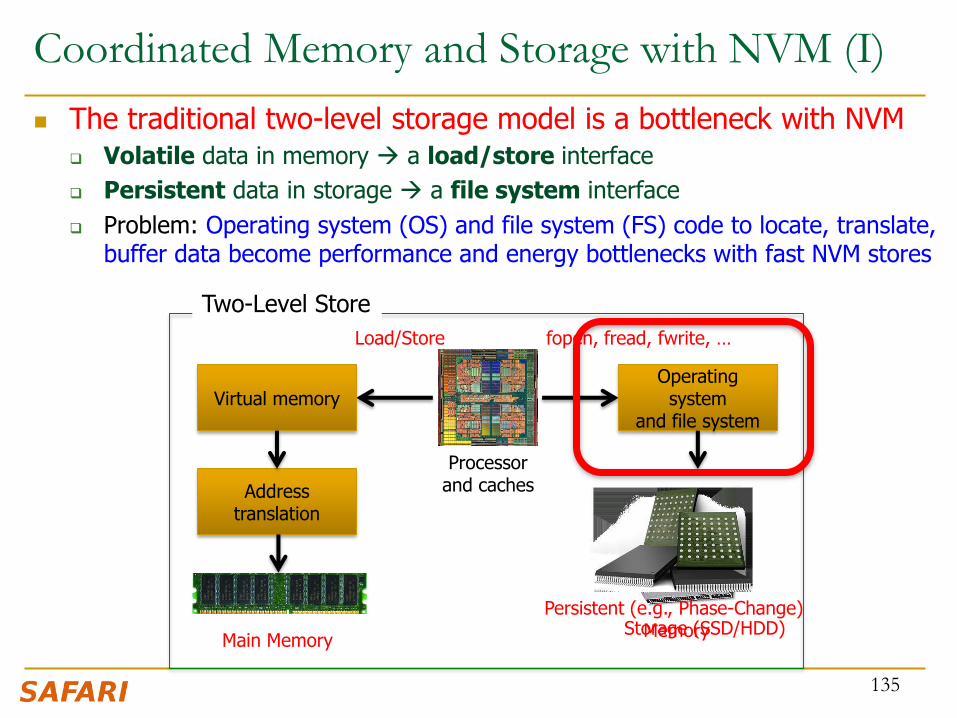
Coordinated Memory and Storage with NVM (I)
The traditional two-level storage model is a bottleneck with NVM Volatile data in memory a load/store interface
Persistent data in storage a file system interface
Problem: Operating system (OS) and file system (FS) code to locate, translate, buffer data become performance and energy bottlenecks with fast NVM stores
135
Two-Level Store
Processorand caches
Main MemoryStorage (SSD/HDD)
Virtual memory
Address translation
Load/Store
Operating system
and file system
fopen, fread, fwrite, …
Persistent (e.g., Phase-Change) Memory
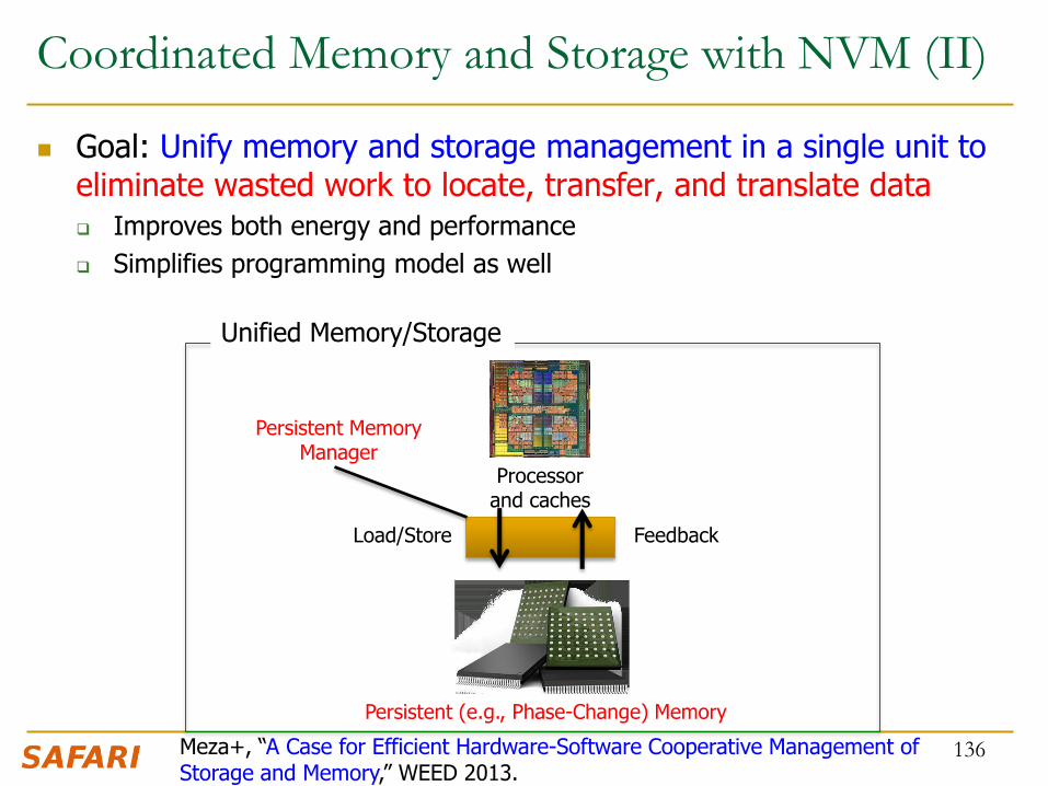
Coordinated Memory and Storage with NVM (II)
Goal: Unify memory and storage management in a single unit to eliminate wasted work to locate, transfer, and translate data
Improves both energy and performance
Simplifies programming model as well
136
Unified Memory/Storage
Processorand caches
Persistent (e.g., Phase-Change) Memory
Load/Store
Persistent MemoryManager
Feedback
Meza+, “A Case for Efficient Hardware-Software Cooperative Management of Storage and Memory,” WEED 2013.

The Persistent Memory Manager (PMM)
Exposes a load/store interface to access persistent data
Applications can directly access persistent memory no conversion,
translation, location overhead for persistent data
Manages data placement, location, persistence, security
To get the best of multiple forms of storage
Manages metadata storage and retrieval
This can lead to overheads that need to be managed
Exposes hooks and interfaces for system software
To enable better data placement and management decisions
Meza+, “A Case for Efficient Hardware-Software Cooperative Management of Storage and Memory,” WEED 2013.
137

The Persistent Memory Manager (PMM)
138
PMM uses access and hint information to allocate, locate, migrate and access data in the heterogeneous array of devices
Persistent objects

Performance Benefits of a Single-Level Store
139
~5X
~24X
Meza+, “A Case for Efficient Hardware-Software Cooperative Management of Storage and Memory,” WEED 2013.
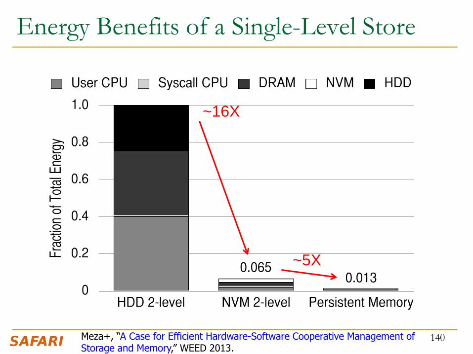
Energy Benefits of a Single-Level Store
140
~5X
~16X
Meza+, “A Case for Efficient Hardware-Software Cooperative Management of Storage and Memory,” WEED 2013.

Agenda
Major Trends Affecting Main Memory
The Memory Scaling Problem and Solution Directions
New Memory Architectures
Enabling Emerging Technologies
How Can We Do Better?
Summary
141
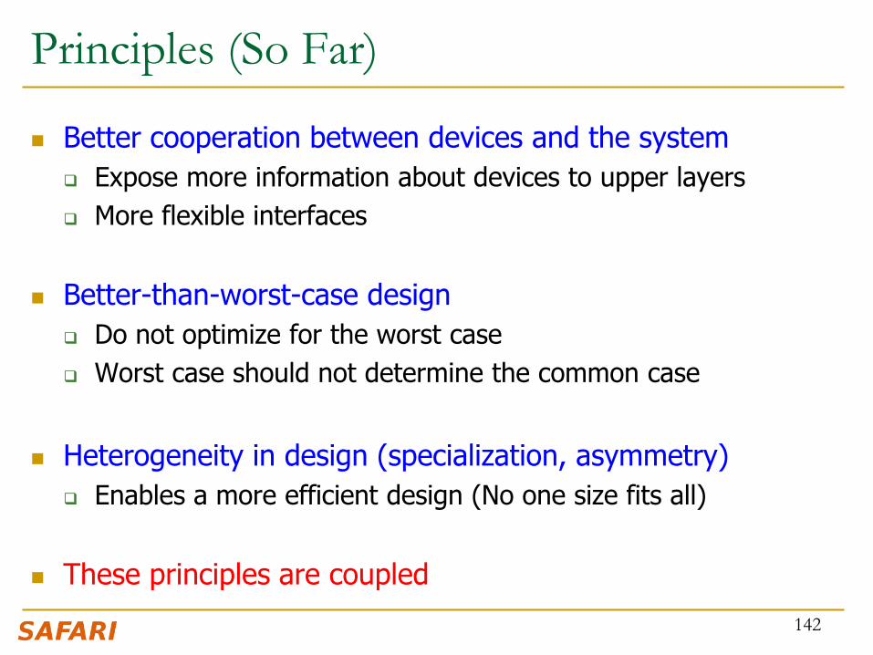
Principles (So Far)
Better cooperation between devices and the system
Expose more information about devices to upper layers
More flexible interfaces
Better-than-worst-case design
Do not optimize for the worst case
Worst case should not determine the common case
Heterogeneity in design (specialization, asymmetry)
Enables a more efficient design (No one size fits all)
These principles are coupled
142

Agenda
Major Trends Affecting Main Memory
The Memory Scaling Problem and Solution Directions
New Memory Architectures
Enabling Emerging Technologies
How Can We Do Better?
Summary
143
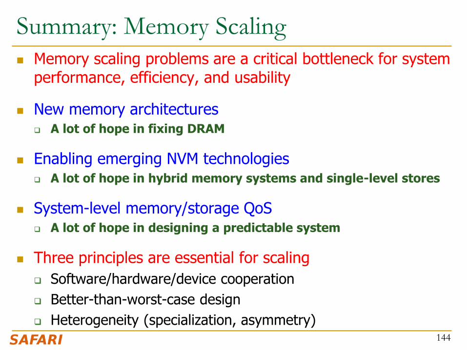
Summary: Memory Scaling
Memory scaling problems are a critical bottleneck for system performance, efficiency, and usability
New memory architectures A lot of hope in fixing DRAM
Enabling emerging NVM technologies A lot of hope in hybrid memory systems and single-level stores
System-level memory/storage QoS A lot of hope in designing a predictable system
Three principles are essential for scaling
Software/hardware/device cooperation
Better-than-worst-case design
Heterogeneity (specialization, asymmetry)144

Acknowledgments
My current and past students and postdocs
Rachata Ausavarungnirun, Abhishek Bhowmick, AmiraliBoroumand, Rui Cai, Yu Cai, Kevin Chang, Saugata Ghose, Kevin Hsieh, Tyler Huberty, Ben Jaiyen, Samira Khan, Jeremie Kim, Yoongu Kim, Yang Li, Jamie Liu, Lavanya Subramanian, Donghyuk Lee, Yixin Luo, Justin Meza, Gennady Pekhimenko, Vivek Seshadri, Lavanya Subramanian, Nandita Vijaykumar, HanBin Yoon, Jishen Zhao, …
My collaborators at CMU
Greg Ganger, Phil Gibbons, Mor Harchol-Balter, James Hoe, Mike Kozuch, Ken Mai, Todd Mowry, …
My collaborators elsewhere
Can Alkan, Chita Das, Sriram Govindan, Norm Jouppi, MahmutKandemir, Konrad Lai, Yale Patt, Moinuddin Qureshi, Partha Ranganathan, Bikash Sharma, Kushagra Vaid, Chris Wilkerson, …
145

Funding Acknowledgments
NSF
GSRC
SRC
CyLab
AMD, Google, Facebook, HP Labs, Huawei, IBM, Intel, Microsoft, Nvidia, Oracle, Qualcomm, Rambus, Samsung, Seagate, VMware
146

Open Source Tools Rowhammer
https://github.com/CMU-SAFARI/rowhammer
Ramulator
https://github.com/CMU-SAFARI/ramulator
MemSim
https://github.com/CMU-SAFARI/memsim
NOCulator
https://github.com/CMU-SAFARI/NOCulator
DRAM Error Model
http://www.ece.cmu.edu/~safari/tools/memerr/index.html
Other open-source software from my group
https://github.com/CMU-SAFARI/
http://www.ece.cmu.edu/~safari/tools.html147
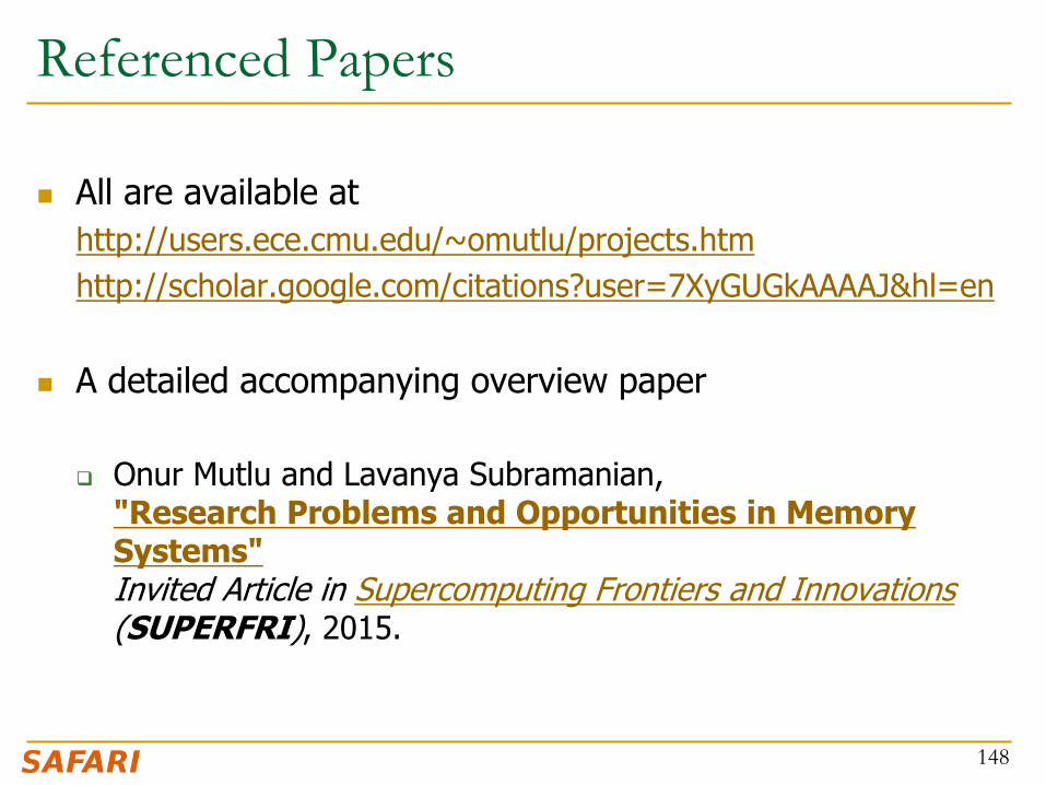
Referenced Papers
All are available at
http://users.ece.cmu.edu/~omutlu/projects.htm
http://scholar.google.com/citations?user=7XyGUGkAAAAJ&hl=en
A detailed accompanying overview paper
Onur Mutlu and Lavanya Subramanian,"Research Problems and Opportunities in Memory Systems"Invited Article in Supercomputing Frontiers and Innovations(SUPERFRI), 2015.
148

Related Videos and Course Materials
Undergraduate Computer Architecture Course Lecture Videos (2013, 2014, 2015)
Undergraduate Computer Architecture Course Materials (2013, 2014, 2015)
Graduate Computer Architecture Course Materials(Lecture Videos)
Parallel Computer Architecture Course Materials(Lecture Videos)
Memory Systems Short Course Materials
(Lecture Video on Main Memory and DRAM Basics)149

Rethinking Memory System Design
(for Data-Intensive Computing)
Prof. Onur Mutlu
18-740 Recitation 2
September 8, 2015
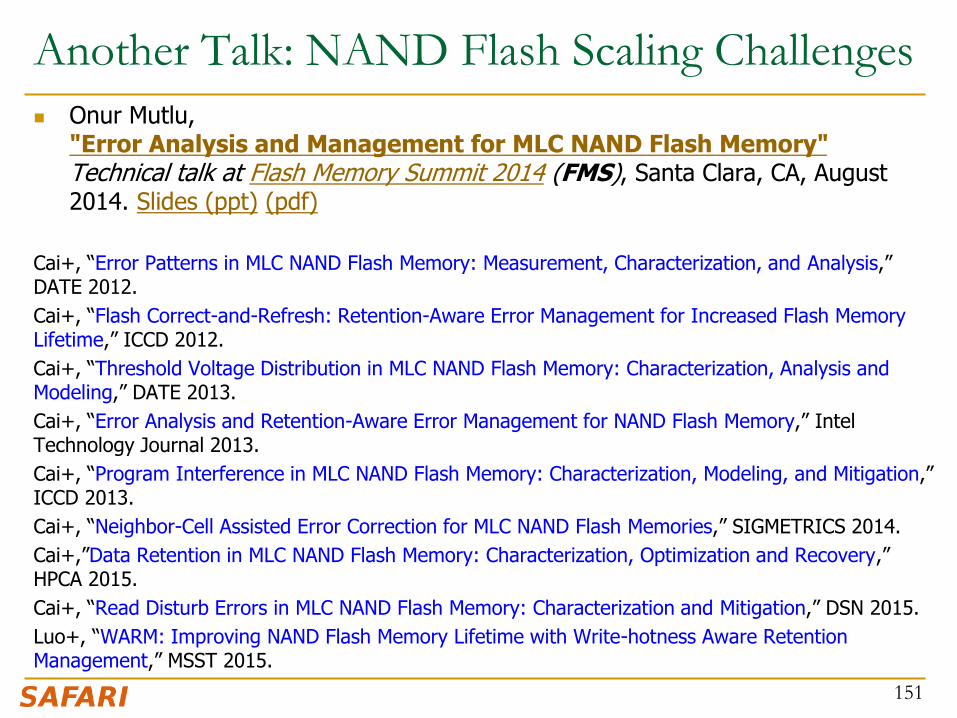
Another Talk: NAND Flash Scaling Challenges
Onur Mutlu,"Error Analysis and Management for MLC NAND Flash Memory"Technical talk at Flash Memory Summit 2014 (FMS), Santa Clara, CA, August 2014. Slides (ppt) (pdf)
Cai+, “Error Patterns in MLC NAND Flash Memory: Measurement, Characterization, and Analysis,” DATE 2012.
Cai+, “Flash Correct-and-Refresh: Retention-Aware Error Management for Increased Flash Memory Lifetime,” ICCD 2012.
Cai+, “Threshold Voltage Distribution in MLC NAND Flash Memory: Characterization, Analysis and Modeling,” DATE 2013.
Cai+, “Error Analysis and Retention-Aware Error Management for NAND Flash Memory,” Intel Technology Journal 2013.
Cai+, “Program Interference in MLC NAND Flash Memory: Characterization, Modeling, and Mitigation,” ICCD 2013.
Cai+, “Neighbor-Cell Assisted Error Correction for MLC NAND Flash Memories,” SIGMETRICS 2014.
Cai+,”Data Retention in MLC NAND Flash Memory: Characterization, Optimization and Recovery,” HPCA 2015.
Cai+, “Read Disturb Errors in MLC NAND Flash Memory: Characterization and Mitigation,” DSN 2015.
Luo+, “WARM: Improving NAND Flash Memory Lifetime with Write-hotness Aware Retention Management,” MSST 2015.
151

Experimental Infrastructure (Flash)
152
USB Jack
Virtex-II Pro
(USB controller)
Virtex-V FPGA
(NAND Controller)
HAPS-52 Mother Board
USB Daughter Board
NAND Daughter Board
3x-nm
NAND Flash
[Cai+, DATE 2012, ICCD 2012, DATE 2013, ITJ 2013, ICCD 2013, SIGMETRICS 2014, HPCA 2015, DSN 2015, MSST 2015]