Embed Size (px)
Citation preview
1.5 – 4.0 GHz High Linearity LNA
BLB03
1
Rev. B
BeRex website: www.berex.com email: [email protected]
Specifications and information are subject to change and products may be discontinued without notice. BeRex is a trademark of BeRex.
All other trademarks are the property of their respective owners. © 2018 BeRex
Pre
limin
ary
Dat
ash
eet
• Operated at 3.0V and 5.0V • 35.5 dBm Output IP3 at 0dBm/tone at 3500MHz • 16.4 dB Gain at 3500 MHz • 20.1 dBm P1dB at 3500MHz • 0.67 dB NF at 3500MHz • Fast shut down to support TDD systems • Lead-free/Green/RoHS Compliant DFN 8L 2x2 Package
BeRex’s BLB03 is a high linearity LNA, based on GaAs material with E-pHEMT process and pack-aged in a RoHS-compliant DFN 8L 2x2 mm2 Surface mount package. It is designed for use where low noise and high linearity are required and features low noise and high OIP3 at Frequency range of 1.5~4.0GHz. It can be used in fast shutdown switching speed for TD-LTE application. All devices are 100% RF/DC tested and classified as HBM ESD Class 1C.
Product Description
Device Features
• Base station Infrastructure
• Commercial/Industrial/Military wireless system
• TDD or FDD LTE system/5G NR
Applications
Applications Circuit
Typical Performance1
1 Device performance _ measured on BeRex’s evaluation board at 25°C, 50 Ω system.
BOM 5V Value 3V Value 5V Value 3V Value
Freq 1.5~3G 1.5~3G 3~4G 3~4G
C1,C2,C3 20pF 20pF 20pF 20pF
C4 N/A N/A 0.3pF 0.3pF
R1 9.1Kohm 6.8Kohm 9.1Kohm 6.8Kohm
R2 3 ohm 3 ohm 3 ohm 3 ohm
L1 15nH 15nH 15nH 15nH
L2 8.2nH 8.2nH 8.2nH 8.2nH
Min. Typical Max. Unit
Bandwidth 1500 4000 MHz
Id @ (Vd = 5.0V) 47 57 67 mA
Id @ (Vd = 3.0V) 30 34 38
dG/dT -0.008 dB/°C
RTH 34.1 °C/W
Parameter Frequency Unit
Vd = 5V 1850 2140 2650 3500 MHz
Gain 20.3 19.5 18 16.4 dB
S11 -14.4 -15.1 -15.1 -12.9 dB
S22 -6.8 -7.3 -7.8 -10.5 dB
OIP32 33.9 34.3 35.8 35.5 dBm
P1dB 20.9 21.2 21 20.1 dBm
Noise Figure 0.32 0.36 0.45 0.67 dB
2 OIP3 _measured with two tones at an output power of 0 dBm/tone separated by 1 MHz. C1 C2RF In RF Out
Vd
L2L1
R1 R2
C3
BLB03
Vsd
C4
1
2
3
4
8
7
6
5
Parameter Frequency Unit
Vd = 3V 1850 2140 2650 3500 MHz
Gain 19.5 18.6 17 15.7 dB
S11 -11.9 -12.7 -12.7 -10.6 dB
S22 -7.0 -7.4 -7.8 -11.2 dB
OIP32 29.6 29.6 30.3 30.8 dBm
P1dB 16.5 16.8 16.6 15.8 dBm
Noise Figure 0.31 0.38 0.48 0.66 dB
3 Noise Figure data has input trace loss de-embedded.

1.5 – 4.0 GHz High Linearity LNA
BLB03
2
Rev. B
BeRex website: www.berex.com email: [email protected]
Specifications and information are subject to change and products may be discontinued without notice. BeRex is a trademark of BeRex.
All other trademarks are the property of their respective owners. © 2018 BeRex
Pre
limin
ary
Dat
ash
eet
Paramter Condition Min. Typical Max. Unit
Shutdown Control On state 0 0.9 V
Off state(shutdown) 1 2.5 V
Current, IDD
On state 5V 47 57 67 mA
On state 3V 30 34 38 mA
Off state(shutdown) 7 mA
Shutdown pin current,Isd 1V ≤ Vsd < 2.5V 150 uA
Switching Time Rise time(10% to 90%) 140 ns
Fall time(90% to 10%) 40 ns
Absolute Maximum Ratings
Operation of this device above any of these parameters may result in permanent damage.
Parameter Unit Rating
Operating Case Temperature °C -40 to +105
Storage Temperature °C -55 to +155
Junction Temperature °C +220
Operating Voltage V +6
Supply Current mA 120
Input RF Power dBm 21
Device performance _ measured on BeRex’s evaluation board at 25°C, 50 Ω system.
V-I Characteristics

1.5 – 4.0 GHz High Linearity LNA
BLB03
3
Rev. B
BeRex website: www.berex.com email: [email protected]
Specifications and information are subject to change and products may be discontinued without notice. BeRex is a trademark of BeRex.
All other trademarks are the property of their respective owners. © 2018 BeRex
Pre
limin
ary
Dat
ash
eet
*Dielectric constant _ 4.2 *RF pattern width 24mil *16mil thick FR4 PCB
PCB Mounting
Pin Configuration

1.5 – 4.0 GHz High Linearity LNA
BLB03
4
Rev. B
BeRex website: www.berex.com email: [email protected]
Specifications and information are subject to change and products may be discontinued without notice. BeRex is a trademark of BeRex.
All other trademarks are the property of their respective owners. © 2018 BeRex
Pre
limin
ary
Dat
ash
eet
Typical Device Data
S-parameters (Vd=5.0V, Id=57mA , T=25°C)
S-parameters (Vd=3.0V, Id=34mA, T=25°C)

1.5 – 4.0 GHz High Linearity LNA
BLB03
5
Rev. B
BeRex website: www.berex.com email: [email protected]
Specifications and information are subject to change and products may be discontinued without notice. BeRex is a trademark of BeRex.
All other trademarks are the property of their respective owners. © 2018 BeRex
Pre
limin
ary
Dat
ash
eet
S-Parameter
(Vd=5.0V,Id = 57mA, T = 25 °C, calibrated to device leads)
Freq
[MHz]
S11
Mag
S11
Ang
S21
Mag
S21
Ang
S12
Mag
S12
Ang
S22
Mag
S22
Ang
1400 0.22 -48.10 12.57 138.29 0.025 50.66 0.50 59.09
1600 0.24 -63.52 11.77 122.96 0.026 40.26 0.50 43.40
1800 0.25 -71.32 10.95 110.41 0.027 35.05 0.49 28.03
2000 0.24 -76.46 10.33 98.67 0.029 35.60 0.50 14.54
2200 0.24 -80.73 9.69 88.18 0.029 29.61 0.50 1.12
2400 0.23 -85.23 8.81 77.72 0.028 27.96 0.50 -11.30
2600 0.24 -87.56 7.98 70.34 0.029 22.55 0.49 -22.57
2800 0.24 -92.60 7.49 63.96 0.030 24.65 0.51 -29.18
3000 0.24 -96.30 7.06 58.41 0.031 23.03 0.54 -39.12
3200 0.24 -100.78 6.78 50.86 0.032 21.35 0.55 -48.95
3400 0.25 -103.61 6.55 44.42 0.032 17.00 0.58 -57.57
3600 0.25 -105.48 6.23 37.65 0.032 13.75 0.60 -65.81
3800 0.27 -108.04 5.99 31.44 0.034 13.23 0.63 -73.33
4000 0.28 -108.31 5.81 25.18 0.033 6.89 0.65 -80.04
(Vd=3.0V,Id = 34mA, T = 25 °C, calibrated to device leads)
Freq
[MHz]
S11
Mag
S11
Ang
S21
Mag
S21
Ang
S12
Mag
S12
Ang
S22
Mag
S22
Ang
1400 0.27 -54.12 11.68 138.84 0.027 48.70 0.49 56.43
1600 0.29 -69.63 10.95 123.29 0.028 42.06 0.48 40.52
1800 0.29 -78.87 10.14 110.55 0.027 42.89 0.47 24.77
2000 0.28 -85.20 9.60 98.75 0.030 38.74 0.47 11.24
2200 0.28 -89.50 9.01 88.19 0.032 31.08 0.49 -1.69
2400 0.27 -93.83 8.17 77.62 0.031 30.36 0.49 -14.12
2600 0.27 -97.66 7.41 69.90 0.032 26.40 0.48 -25.52
2800 0.27 -102.26 6.97 63.63 0.032 24.81 0.50 -32.82
3000 0.26 -106.54 6.59 57.74 0.033 22.43 0.52 -42.44
3200 0.26 -111.13 6.32 49.91 0.035 17.74 0.54 -52.02
3400 0.27 -114.33 6.09 43.48 0.036 17.81 0.57 -60.85
3600 0.27 -116.53 5.78 36.40 0.036 13.11 0.59 -68.74
3800 0.28 -118.25 5.59 30.09 0.037 13.41 0.62 -76.76
4000 0.29 -119.02 5.41 23.70 0.040 8.86 0.65 -82.83

1.5 – 4.0 GHz High Linearity LNA
BLB03
6
Rev. B
BeRex website: www.berex.com email: [email protected]
Specifications and information are subject to change and products may be discontinued without notice. BeRex is a trademark of BeRex.
All other trademarks are the property of their respective owners. © 2018 BeRex
Pre
limin
ary
Dat
ash
eet
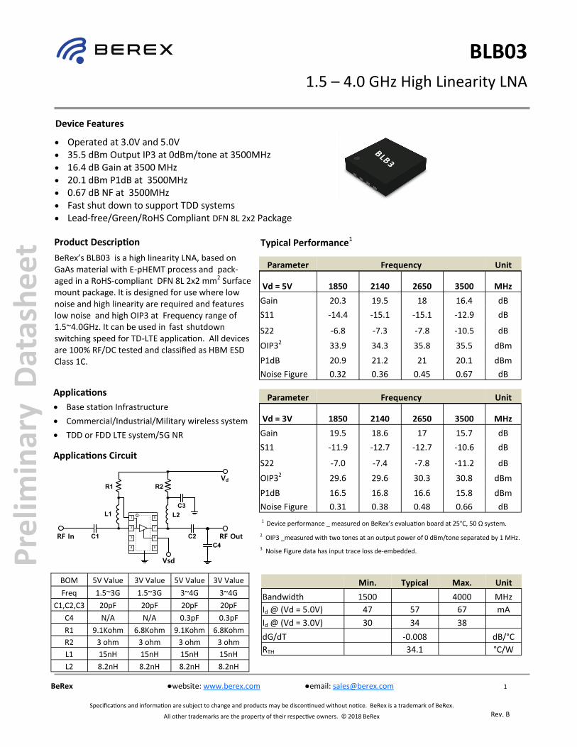
Vd = 5.0V, Idq = 57mA
Device Performance

1.5 – 4.0 GHz High Linearity LNA
BLB03
7
Rev. B
BeRex website: www.berex.com email: [email protected]
Specifications and information are subject to change and products may be discontinued without notice. BeRex is a trademark of BeRex.
All other trademarks are the property of their respective owners. © 2018 BeRex
Pre
limin
ary
Dat
ash
eet
Device Performance Vd = 5.0V, Idq = 57mA
Noise Figure Temperature Performance
(Vd = 5.0V, Idq = 57mA)
Freq MHz 1850 2140 2650 3500
Temp
[°C]
-40 0.34 0.35 0.41 0.60
+25 0.32 0.36 0.45 0.67
+105 0.47 0.51 0.63 0.95
* Noise Figure data has input trace loss de-embedded.
1.5 – 4.0 GHz High Linearity LNA
BLB03
8
Rev. B
BeRex website: www.berex.com email: [email protected]
Specifications and information are subject to change and products may be discontinued without notice. BeRex is a trademark of BeRex.
All other trademarks are the property of their respective owners. © 2018 BeRex
Pre
limin
ary
Dat
ash
eet
Device Performance Vd = 5.0V, Idq = 57mA
Noise Figure Temperature Performance
(Vd = 5.0V, Idq = 57mA)
Freq MHz 1850 2140 2650 3500
Temp
[°C]
-40 0.34 0.35 0.41 0.60
+25 0.32 0.36 0.45 0.67
+105 0.47 0.51 0.63 0.95
* Noise Figure data has input trace loss de-embedded.

1.5 – 4.0 GHz High Linearity LNA
BLB03
9
Rev. B
BeRex website: www.berex.com email: [email protected]
Specifications and information are subject to change and products may be discontinued without notice. BeRex is a trademark of BeRex.
All other trademarks are the property of their respective owners. © 2018 BeRex
Pre
limin
ary
Dat
ash
eet
Device Performance Vd = 5.0V, Idq = 57mA
Noise Figure Temperature Performance
(Vd = 5.0V, Idq = 57mA)
Freq MHz 1850 2140 2650 3500
Temp
[°C]
-40 0.34 0.35 0.41 0.60
+25 0.32 0.36 0.45 0.67
+105 0.47 0.51 0.63 0.95
* Noise Figure data has input trace loss de-embedded.

1.5 – 4.0 GHz High Linearity LNA
BLB03
10
Rev. B
BeRex website: www.berex.com email: [email protected]
Specifications and information are subject to change and products may be discontinued without notice. BeRex is a trademark of BeRex.
All other trademarks are the property of their respective owners. © 2018 BeRex
Pre
limin
ary
Dat
ash
eet
Vd = 5.0V, Idq = 57mA
Device Performance

1.5 – 4.0 GHz High Linearity LNA
BLB03
11
Rev. B
BeRex website: www.berex.com email: [email protected]
Specifications and information are subject to change and products may be discontinued without notice. BeRex is a trademark of BeRex.
All other trademarks are the property of their respective owners. © 2018 BeRex
Pre
limin
ary
Dat
ash
eet
Device Performance Vd = 5.0V, Idq = 57mA
Noise Figure Temperature Performance
(Vd = 5.0V, Idq = 57mA)
Freq MHz 1850 2140 2650 3500
Temp
[°C]
-40 0.34 0.35 0.41 0.60
+25 0.32 0.36 0.45 0.67
+105 0.47 0.51 0.63 0.95
* Noise Figure data has input trace loss de-embedded.

1.5 – 4.0 GHz High Linearity LNA
BLB03
12
Rev. B
BeRex website: www.berex.com email: [email protected]
Specifications and information are subject to change and products may be discontinued without notice. BeRex is a trademark of BeRex.
All other trademarks are the property of their respective owners. © 2018 BeRex
Pre
limin
ary
Dat
ash
eet
Vd = 3.0V, Idq = 34mA
Device Performance

1.5 – 4.0 GHz High Linearity LNA
BLB03
13
Rev. B
BeRex website: www.berex.com email: [email protected]
Specifications and information are subject to change and products may be discontinued without notice. BeRex is a trademark of BeRex.
All other trademarks are the property of their respective owners. © 2018 BeRex
Pre
limin
ary
Dat
ash
eet
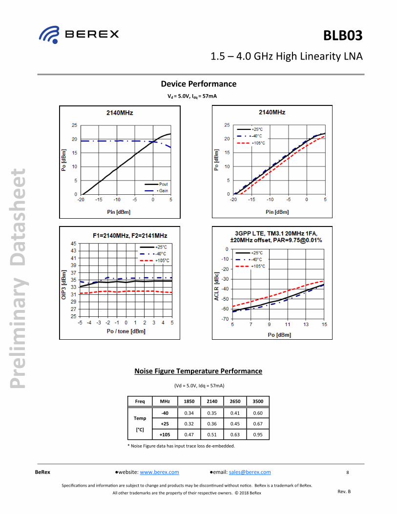
Device Performance Vd = 3.0V, Idq = 34mA
Noise Figure Temperature Performance
(Vd = 3.0V, Idq = 34mA)
Freq MHz 1850 2140 2650 3500
Temp
[°C]
-40 0.28 0.32 0.40 0.61
+25 0.31 0.38 0.48 0.66
+105 0.44 0.50 0.64 0.96
* Noise Figure data has input trace loss de-embedded.

1.5 – 4.0 GHz High Linearity LNA
BLB03
14
Rev. B
BeRex website: www.berex.com email: [email protected]
Specifications and information are subject to change and products may be discontinued without notice. BeRex is a trademark of BeRex.
All other trademarks are the property of their respective owners. © 2018 BeRex
Pre
limin
ary
Dat
ash
eet
Device Performance Vd = 3.0V, Idq = 34mA
Noise Figure Temperature Performance
(Vd = 3.0V, Idq = 34mA)
Freq MHz 1850 2140 2650 3500
Temp
[°C]
-40 0.28 0.32 0.40 0.61
+25 0.31 0.38 0.48 0.66
+105 0.44 0.50 0.64 0.96
* Noise Figure data has input trace loss de-embedded.
1.5 – 4.0 GHz High Linearity LNA
BLB03
15
Rev. B
BeRex website: www.berex.com email: [email protected]
Specifications and information are subject to change and products may be discontinued without notice. BeRex is a trademark of BeRex.
All other trademarks are the property of their respective owners. © 2018 BeRex
Pre
limin
ary
Dat
ash
eet
Device Performance Vd = 3.0V, Idq = 34mA
Noise Figure Temperature Performance
(Vd = 3.0V, Idq = 34mA)
Freq MHz 1850 2140 2650 3500
Temp
[°C]
-40 0.28 0.32 0.40 0.61
+25 0.31 0.38 0.48 0.66
+105 0.44 0.50 0.64 0.96
* Noise Figure data has input trace loss de-embedded.

1.5 – 4.0 GHz High Linearity LNA
BLB03
16
Rev. B
BeRex website: www.berex.com email: [email protected]
Specifications and information are subject to change and products may be discontinued without notice. BeRex is a trademark of BeRex.
All other trademarks are the property of their respective owners. © 2018 BeRex
Pre
limin
ary
Dat
ash
eet
Vd = 3.0V, Idq = 34mA
Device Performance

1.5 – 4.0 GHz High Linearity LNA
BLB03
17
Rev. B
BeRex website: www.berex.com email: [email protected]
Specifications and information are subject to change and products may be discontinued without notice. BeRex is a trademark of BeRex.
All other trademarks are the property of their respective owners. © 2018 BeRex
Pre
limin
ary
Dat
ash
eet
Device Performance Vd = 3.0V, Idq = 34mA
Noise Figure Temperature Performance
(Vd = 3.0V, Idq = 34mA)
Freq MHz 1850 2140 2650 3500
Temp
[°C]
-40 0.28 0.32 0.40 0.61
+25 0.31 0.38 0.48 0.66
+105 0.44 0.50 0.64 0.96
* Noise Figure data has input trace loss de-embedded.

1.5 – 4.0 GHz High Linearity LNA
BLB03
18
Rev. B
BeRex website: www.berex.com email: [email protected]
Specifications and information are subject to change and products may be discontinued without notice. BeRex is a trademark of BeRex.
All other trademarks are the property of their respective owners. © 2018 BeRex
Pre
limin
ary
Dat
ash
eet
Package Outline Dimension
Suggested PCB Land Pattern and PAD Layout
PCB Land Pattern
Note : All dimension _ millimeters
PCB lay out _ on BeRex website

1.5 – 4.0 GHz High Linearity LNA
BLB03
19
Rev. B
BeRex website: www.berex.com email: [email protected]
Specifications and information are subject to change and products may be discontinued without notice. BeRex is a trademark of BeRex.
All other trademarks are the property of their respective owners. © 2018 BeRex
Pre
limin
ary
Dat
ash
eet
Lead plating finish
100% Tin Matte finish
(All BeRex products undergoes a 1 hour, 150 degree C, Anneal bake to eliminate thin whisker growth
concerns.)
MSL / ESD Rating
ESD Rating:
Value:
Test:
Standard:
MSL Rating:
Standard:
Class 1C
Passes ≥ 1000V to < 2000 V
Human Body Model (HBM)
JEDEC Standard JESD22-A114B
Level 1 at +265°C convection reflow
JEDEC Standard J-STD-020
NATO CAGE code:
2 N 9 6 F
Tape & Reel Package Marking
XX = Wafer No.
DFN 8L 2x2 Packaging information:
Tape Width (mm): 8
Reel Size (inches): 7
Device Cavity Pitch (mm): 4
Devices Per Reel: 3000