Embed Size (px)
Citation preview

Dr. Ananthaiah. J, Assistant professor
14. Assignment topics with materials
1. Explain Davisson and Germer experiment ?
Initial atomic models proposed by scientists could only explain the particle nature of electrons
but failed to explain the properties related to their wave nature. C.J. Davisson and L.H. Germer
in the year 1927 carried out an experiment, popularly known as Davisson Germer experiment to
explain the wave nature of electrons through electron diffraction. In this article, we will learn
about observations and conclusions of Davisson Germer experiment.
Experimental setup of Davisson Germer experiment
The experimental arrangement of Davisson Germer experiment is discussed below:
An electron gun was taken, which comprised of a tungsten filament F, coated with
barium oxide and heated by a low voltage power supply.
Electrons emitted from this electron gun were accelerated to a desired velocity by
applying suitable potential difference from a high voltage power supply.
These emitted electrons were made to pass through a cylinder perforated with fine holes
along its axis, thus producing a fine collimated beam.
Dr. Ananthaiah. J, Assistant professor
This beam produced from the cylinder is made to fall on the surface of a nickel crystal.
This leads to scattering of electrons in various directions.
The intensity of the beam of electrons is measured by the electron detector which is
connected to a sensitive galvanometer (to record the current) and can be moved on a
circular scale.
The intensity of the scattered electron beam is measured for different values of angle of
scattering,
detector on the circular scale at different positions.
Observations of Davisson Germer experiment:
Observations of Davisson Germer experiment are listed below:
By varying accelerating potential difference, we finally obtained the variation of the
voltage was varied from 44V to 68 V.
A strong peak was noticed in the intensity (I) of the scattered electron for an accelerating
This peak can be explained as a result of the constructive interference of electrons
scattered from different layers of the regularly spaced atoms of the crystals.
The wavelength of matter waves was calculated with the help of electron diffraction,
which measured to be 0.165 nm.
Co-relating Davisson Germer experiment and de Broglie relation:
2. Explain about N Type Semiconductor ?
When a small amount of pentavalent impurity (group V element) is added to a pure
semiconductor, it becomes a n semiconductor.

Dr. Ananthaiah. J, Assistant professor
Such impurities are known as donor impurities because they donate the free electrons to the
semiconductor crystal.
A pentavalent impurity (arsenic) having five valance electrons is added to a pure semiconducting
material having four valance electrons (silicon or germanium).
The four valance electrons of the impurity atoms bond with four valance electrons of the
semiconductor atom and remaining 1 electron of the impurity atom is left free as shown fig.
Therefore number of free electrons increases, as the electrons are produced in excess, they the
majority charge carrier in n type semiconductor and holes are the majority charge carriers.
Since electrons are donated in this type of semiconductor the energy level of these donated
electrons is called donor .
P Type Semiconductor P Type semiconductor is obtained by doping an intrinsic semiconductor with trivalent (3
electrons in valance band)impurity atoms like boron, gallium, indium etc.,
The three valance electrons of the impurity atom pairs with three valence electrons of the r
energy level (Ed) Semiconductor atom and one position of the impurity atom remains vacant, this is called hole as
shown in fig
Therefore the number of holes increased with impurity atoms added to it. Since holes are
produced in excess, they are the majority charge carriers in p type semiconductor and electrons
are the minority charge carriers.
Since the impurity can accept the electrons this energy level is called acceptor energy level (Ea)
and is present just above the valence band.
Intrinsic Semiconductors Electrons and Holes We know that, at 0K intrinsic pure semiconductor behaves as insulator. But as temperature
increases some electron move from valance band to conduction band as shown in fig. therefore
both electrons in conduction band and holes in valance band will contribute to electrical
conductivity. Therefore the carrier concentration (or) density of electrons (ne) and holes (nh) has
to be calculated.

Dr. Ananthaiah. J, Assistant professor
Assume that electron in the conduction band as a free electron of mass m*e and the hole in the
valance band behave as a free particle of mass m*h. The electrons in the conduction band
- in figure. Here Ec represents the lowest energy level of conduction band
Ev represents the highest energy level of the valance band.
3. Briefly discuss about Solar Cell
Solar cell, also called photovoltaic cell, any device that directly converts the energy of light into
electrical energy through the photovoltaic effect.
The overwhelming majority of solar cells are fabricated from silicon with
increasing efficiency and lowering cost as the materials range from amorphous (noncrystalline)
to polycrystalline to crystalline (single crystal) silicon forms. Unlike batteries or fuel cells, solar
cells do not utilize chemical reactions or require fuel to produce electric power, and,
unlike electric generators, they do not have any moving parts.
Solar cells can be arranged into large groupings called arrays.
These arrays, composed of many thousands of individual cells, can function as central electric
power stations, converting sunlight into electrical energy for distribution to industrial,
commercial, and residential users.
Solar cells in much smaller configurations, commonly referred to as solar cell panels or simply
solar panels, have been installed by homeowners on their rooftops to replace or augment their
conventional electric supply.
Solar cell panels also are used to provide electric power in many remote terrestrial locations
where conventional electric power sources are either unavailable or prohibitively expensive to

Dr. Ananthaiah. J, Assistant professor
install. Because they have no moving parts that could need maintenance or fuels that would
require replenishment, solar cells provide power for most space installations, from
communications and weather satellites to space stations. (Solar power is insufficient for space
probes sent to the outer planets of the solar system or into interstellar space, however, because of
the diffusionof radiant energy with distance from the Sun.) Solar cells have also been used in
consumer products, such as electronic toys, handheld calculators, and portable radios. Solar cells
used in devices of this kind may utilize artificial light (e.g., from incandescent and fluorescent
lamps) as well as sunlight.
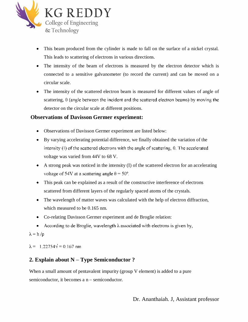
4. Expline the devision of amplitude and coherence? Two coherence waves are obtained by dividing the amplitude of a beam originating from a
common source. This is done either by partial reflection or refraction. These coherent beams
travel in different paths and then brought together to produce interference.
Fig :- -example for amplitudedivision
Dr. Ananthaiah. J, Assistant professor
Division of wave front:-
Two coherence waves are obtained by dividing the amplitude of a beam originating from a
common source. This is occurring due to the mirrors, biprisms or lenses.
5. What are the applications of lasers ?
Applications of lasers:
Lasers in communication and Atmospheric science:-
1. More amount data can be sent because of large band width.
2. More channels
3. Signals cannot be trapped
4. Highly directional, hence greater potential use in space crafts and submarines.

Dr. Ananthaiah. J, Assistant professor
Lasers in computers:
1. In LAN, data transfer from one computer to other for short time.
2.
Lasers in Industry:
1. Blast holes in hard materials like diamond, hard stell etc.
2. Source as intense heat
3. To measure distance to making maps by surveyors
4. To cut teeth saws, drill in surgical needle, guide bulldozers
5. In welding: Purity of the material is not altered.
Lasers in Scientific Research:-
1. To separate isotopes of uranium.
2. To create plasma, this may help the scientists to control nuclear fusion reaction.
3. To create 3D-photography called holography.
4. Recording and reconstruction of hologram to data storage.
Lasers in Medicine:
1. To remove diseased body tissues.
2. Retinal detachment by eye specialist.
3. To instantly weld injured muscles, ligaments without use of the heat.
4. Argon and CO2 lasers are used in liver and lungs treatment.
5. To elimination of moles and tumors on skin tissues.

Dr. Ananthaiah. J, Assistant professor
6. Explain acceptance cone and numerical aperture?
Acceptance cone:
Rotating the Acceptance angle about the fiber axis describes the
Acceptance Cone of the fiber.
Light launched at the fiber end within this Acceptance Cone alone
will be accepted and propagated to the other end of the fiber by
total internal reflection.
7. Explain types of magnetic materials?
Types of Magnetism
its magnitude and sign.
-magnetism
-magnetism
-magnetism.
Anti-ferro-magnetism and ferri-magnetisms are considered as subclasses of ferro-magnetism. Dia-magnetism
-permanent.
nbalancing their orbiting electrons, and creates small magnetic dipoles within atoms which oppose the applied field. This action produces a negative magnetic effect known as diamagnetism.
irection is opposite to the direction of applied field (H).
of -10-5.
Dr. Ananthaiah. J, Assistant professor
perature. Para-magnetism
-up with the field, resulting in a positive magnetization. However, the dipoles do not interact.
y in the presence of a magnetic field are called para-magnetic, and the effect is termed as para-magnetism.
no net magnetization.
field is applied dipoles line-up with the field, resulting in a positive magnetization.
of the dipoles.
the magnetic field is removed.
decreases the paramagnetic effect.
-magnetism is produced in many materials like aluminium, calcium, titanium, alloys of copper.
-5 to +10-2. Ferro-magnetism
- and para- magnetic materials are considered as non-magnetic because they exhibit magnetization only in presence of an external field.
-up with the imposed magnetic field due to the exchange interaction or mutual reinforcement of the dipoles. These are chrematistics of ferromagnetism.
-magnetism (Examples: Fe, Co, Ni, Gd) possess magnetic susceptibilities approaching 106
Above the Curie temperature, ferro-magnetic materials behave as para-magnetic materials and their susceptibility is given by the Curie-
here C material constant, T temperature, Tc Curie temperature.

Dr. Ananthaiah. J, Assistant professor
15. Tutorial topics and questions
Topic:- Classification of magnetic materials
Questions:-
1). What is dia magnetic material ?
2). Explain difference between para and ferro magnetic materials ?
16. Unit wise Question bank

Dr. Ananthaiah. J, Assistant professor
Unit-I Quantum Mechanics
2 marks question and answers
1). Write down the Schrodinger wave equation for a particle in a three dimensional box.
Ans: - 2 2 2 2 2 2 2
2).
1 has the significance of probability.
3). The energy expression for the electron in a one dimensional potential box is given by En = (n2h2/8ma2). Derive the important conclusions from this equation.
Ans: 1. Energy is quantized;
2. n = 0 is not allowed
3. Smallest energy is for n = 1 i.e., E1 = Eo =h2/8ma2
4). Why is the wave nature of matter not more apparent to our daily life?
6.626X10-
34 /m*v. The wavelength associated with a particle of mass 1 kg moving with 1m/sec is of the order 10-34m which is very small. If the particle is at rest, then the wavelength is infinity. Hence the wave nature is not more apparent.
5). How can the wmomentum p in the formula imply that the electron is a particle? Ans: Above equation actually connects the two forms of matter (the wave and particle nature). What it says is that f

Dr. Ananthaiah. J, Assistant professor
3 Marks question and answers
1). What is the physical significance of a wave function?
(i) It relates the particles and wave nature of matter elastically.
(ii) The square of the wave function is a measure of the probability of finding the
Particle at a particular position. It cannot predict the exact location of the particle.
(iii) The wave function is a complex quantity, where as the probability is a real and
positive quantity.
(iv) The wave function has no physical meaning.
2 = is real and positive, amplitude may be positive or negative but the
Intensity (square of amplitude) is always real and positive.
2 represents the probability density or probability of finding the particle in
the given region.
2
2 normalized wave function.
2). What is the concept of wave-particle duality? Ans: On the basis of existing experimental facts like interference, diffraction and polarization
it is clear that EM radiation possess wave nature. On the other hand there are experimental
evidences like photoelectric effect, emission and absorption spectra, black body radiation etc.,
photons. Hence, we can conclude that EM radiation has dual character, i.e., in certain
situations it exhibits characteristics of wave, while in other; it shows its particle characteristics. However, both the characteristics can never be observed simultaneously.

Dr. Ananthaiah. J, Assistant professor
3). hypothesis?
Ans.: Acco
it The wavelength of the wave depends upon the momentum of the particle. The de-
Broglie wavelength is given by:
4). State the principle of uncertainty. Ans. It is impossible to measure precisely and
simultaneously both the members of a pair of canonically conjugate variables describing the
behavior The canonically conjugate pairs are position and momentum,
energy and time, angular momentum and angular position etc. In a simplified manner,
position and momentum of a particle at the same instant is a best of the order of the uncertainty
in. The Hei universal and hold for all pairs of conjugate
variables.
5). What is wave function? Ans.: The properties of a system comprised of particles moving in a conservative force field are described by a function, where is a function of position coordinates and time i.e. This function is called the wave function of the system. Hence we can say make up the matter waves is called the wave functioassociated with a moving body at the particular point x, y, z in space at time t is related to the likelihood of finding the body there at that time. The wave function should be finite, continuous and single valued.
5 Marks question and answer
1). Explain Davisson and Germer experiment ?
Initial atomic models proposed by scientists could only explain the particle nature of electrons
but failed to explain the properties related to their wave nature. C.J. Davisson and L.H. Germer
in the year 1927 carried out an experiment, popularly known as Davisson Germer experiment to

Dr. Ananthaiah. J, Assistant professor
explain the wave nature of electrons through electron diffraction. In this article, we will learn
about observations and conclusions of Davisson Germer experiment.
Experimental setup of Davisson Germer experiment.
The experimental arrangement of Davisson Germer experiment is discussed below:
An electron gun was taken, which comprised of a tungsten filament F, coated with barium oxide
and heated by a low voltage power supply.
Electrons emitted from this electron gun were accelerated to a desired velocity by applying
suitable potential difference from a high voltage power supply.
These emitted electrons were made to pass through a cylinder perforated with fine holes along its
axis, thus producing a fine collimated beam.
This beam produced from the cylinder is made to fall on the surface of a nickel crystal. This
leads to scattering of electrons in various directions.
The intensity of the beam of electrons is measured by the electron detector which is connected to
a sensitive galvanometer (to record the current) and can be moved on a circular scale.

Dr. Ananthaiah. J, Assistant professor
The intensity of the scattered electron beam is measured for different values of angle of
detector on the circular scale at different positions.
Observations of Davisson Germer experiment:
Observations of Davisson Germer experiment are listed below:
By varying accelerating potential difference, we finally obtained the variation of the intensity (I)
44V to 68 V.
A strong peak was noticed in the intensity (I) of the scattered electron for an accelerating voltage
This peak can be explained as a result of the constructive interference of electrons scattered from
different layers of the regularly spaced atoms of the crystals.
The wavelength of matter waves was calculated with the help of electron diffraction, which
measured to be 0.165 nm.
Co-relating Davisson Germer experiment and de Broglie relation:
by,
Dr. Ananthaiah. J, Assistant professor
2). Schrodinger time independent wave equation?
Suppose a system of
stationary waves is associated with the particles at any point in space in the neighborhood of
particle.
We know that:

Dr. Ananthaiah. J, Assistant professor

Dr. Ananthaiah. J, Assistant professor
3. Explain about Heisenberg uncertainty principle?
The Heisenberg Uncertainty Principle states that you can never simultaneously know the exact
position and the exact speed of an object. Why not? because everything in the universe behaves
like both a particle and a wave at the same time. The Heisenberg Uncertainty Principle states
that you can never simultaneously know the exact position and the exact speed of an object. Why
not? because everything in the universe behaves like both a particle and a wave at the same
time.

Dr. Ananthaiah. J, Assistant professor
4. Explain about de-Broglie hypothesis ?
The de Broglie equation relates a moving particle's wavelength with its momentum. The de Broglie wavelength is the wavelength , associated with a massive particle and is related to its momentum p, through the Planck constant h.
In other words, you can say that matter also behaves like waves. This is what is called as de Broglie hypothesis.
de Broglie, in his 1924 PhD thesis, proposed that just as light has both wave-like and particle-like properties, electrons also have wave-like properties. The wavelength, , associated with an electron is related to its momentum, p, through the Planck constant,
The relationship is now known to hold for all types of matter: all matter exhibits properties of both particles and waves.
4. What is Photoelectric Effect? The electrons present in the outermost shell of an atom are called valence electrons. The valence electrons have the highest energy level. So they are loosely attached to the parent atom. Applying a small energy is enough to remove the valence electrons from the parent atom. The energy can be supplied through various sources such as electric field, heat, and light.
If the light is used as the energy source to remove the electrons from the metal surface then it is called photoelectric emission or photoelectric effect.
When photons (light) hit the metal surface with a frequency greater than the threshold frequency, the electrons in the material gets sufficient energy and emitted from the metal surface.
In order to emit the electrons from the metal surface, this condition is necessary
The frequency (V) of the incident photon must be greater than the minimum frequency called threshold frequency (V0) i.e., V > V0. Threshold frequency is the minimum frequency needed for photons (light) to emit electrons from the metal surface.
The electrons are emitted from the metal surface if the frequency of the incident photons is greater than the threshold frequency of the material.
The energy of a photon is directly proportional to its frequency. High-frequency photons have the greater energy whereas low-frequency photons have the lesser energy.
If the electron within a material absorbs the entire energy of a high-frequency photon (greater than threshold frequency) and gains more energy than the work function of a material, it is
Dr. Ananthaiah. J, Assistant professor
emitted from the metal surface. Thus, the electrons are emitted from the metal surface, if the incident photons frequency (energy) is greater than the threshold frequency.
If the electron absorbs the energy of a low-frequency photon (less than threshold frequency), it is unable to escape from the material. Because the strong bonding force of the material prevents the emission of the electron. Thus, the electrons are not emitted from the metal surface, if the incident photons frequency (energy) is less than the threshold frequency.
Objective question and answers
1. In order to find the internal structure of nucleus, electrons should be accelerated by voltages up to
A. 105 V B. 107 V C. 109 V D. 1011 V
2. High speed electrons have wavelength of order
A. 10-15 m B. 10-14 m C. 10-16 m D. 10-17 m
3. Wavelength of slow moving neutrons is about
A. 10-34 m B. 10-20 m C. 10-19 m D. 10-10 m
4. High speed electrons from particle detectors are used to determine
A. arrangement of atoms in metals B. diameter of atomic nuclei C. inter atomic distance D. circumference of atomic nuclei
Dr. Ananthaiah. J, Assistant professor
5. Waves associated with electrons are referred to as
A. plasma waves B. UV waves C. gamma rays D. matter waves
6. Frequency below which no electrons are emitted from metal surface is
A. minimum frequency B. angular frequency C. maximum frequency D. threshold frequency
7. According to Newton, the light travels as
A. particles B. waves C. both A and B D. dust
8. In electron diffraction, the rings behave as
A. particles B. waves C. both A and B D. rays
9. Diffraction of slow moving electrons is used to estimate
A. arrangement of atoms in metals B. nature of atoms C. number of atoms in metals D. position of atoms in metalloids
10. Energy of an electron in an atom is
A. quantized B. continuous

Dr. Ananthaiah. J, Assistant professor
C. radial D. randomized
Fill in the blanks question with answers
1. Electrons show diffraction effects because their de Broglie wavelength is similar to--------------------
2. Characteristic properties of waves are-----
3. Wavelength of red color is about----------
4. Quantum of electromagnetic energy is called------
5. In photoelectric effect, electrons should be removed from the--------
6. Light interacts with matter as-----------------
7. When white light is passed through cool gases, the spectra observed is called----
8. In an insulator, the valence band is-----
9. Wavelength of ultraviolet region of electromagnetic spectrum is--------
10. Energy of photon is directly related to the-------
Dr. Ananthaiah. J, Assistant professor
Answers:- 1. c 2. a 3.d 4. b 5.d 6. d 7. a 8.b 9. a 10.a
1. spacing between atomic layers
2. interference 8. fully occupied
3. 7 × 10⁻⁷ m 9. 121 nm
4. photons 10. frequency
5. surface
6. particle
7. absorption line spectra
Dr. Ananthaiah. J, Assistant professor
Unit -II
Semiconductor physics
2. Marks question and answers
1). What is conductor?
An electrical conductor is a substance in which electrical charge carriers, usually, move electron
easily from atom to atom with the application of voltage.
2). How many types of semiconductor?
Mainly semiconductors are two types
1. Intrinsic (Pure) Semiconductors. 2. Extrinsic (Impure) Semiconductors. 2. Based on energy band A semiconductor has nearly empty conduction band and almost filled valance band with very
2). General properties of semiconductors
They are formed by covalent bonds. They have an empty conduction band at 0K. They have almost filled valance band. They have small energy gap. 3). What is Extrinsic semiconductors A semiconductor in extremely impure form, with the addition of impurities is known as extrinsic semiconductors
4). Types of extrinsic semiconductor The extrinsic semiconductors are classified into two types based on the type of impurity added. (i) N type semiconductor (ii) P type semiconductor
Dr. Ananthaiah. J, Assistant professor
3 Marks question and answers
1. Explain about P Type semiconductor ?
P Type semiconductor is obtained by doping an intrinsic semiconductor with trivalent (3 electrons in valance band) impurity atoms like boron, gallium, indium etc.
The three valance electrons of the impurity atom pairs with three valence electrons of the r energy level (Ed) semiconductor atom and one position of the impurity atom remains vacant, this is called hole
Therefore the number of holes increased with impurity atoms added to it. Since holes are
produced in excess, they are the majority charge carriers in p type semiconductor and electrons are the minority charge carriers.
Since the impurity can accept the electrons this energy level is called acceptor energy
level (Ea) and is present just above the valence band. 2.Explain about Depletion region?
No free charge carriers can rest in a position where there is a potential barrier, the regions on either sides of the junction now become completely depleted of any more free carriers in comparison to the N and P type materials further away from the junction. This area around the PN Junction is now called the Depletion Layer.
5. Types of bias? Zero Bias No external voltage potential is applied to the PN junction diode. Reverse Bias The voltage potential is connected negative, (-ve) to the P-type
material and positive, (+ve) to the N-type material across the diode which has the effect of Increasing
Forward Bias The voltage potential is connected positive, (+ve) to the P-type material and negative, (-ve) to the N-type material across the diode which has the effect of Decreasing the PN junction diodes width.
4. What is direct band gap?
The band gap represents the minimum energy difference between the top of the valence band and the bottom of the conduction band. However, the top of the valence band and the bottom of the conduction band are not generally at the same value of the electron momentum. In a direct band gap semiconductor, the top of the valence band and the bottom of the conduction band occur at the same value of momentum.

Dr. Ananthaiah. J, Assistant professor
5. What is In direct band gap?
The maximum energy of the valence band occurs at a different value of momentum to the minimum in the conduction band energy.
The difference between the two is most important in optical devices. As has been
mentioned in the section charge carries in semiconductor, a photon can provide the energy to produce an electron-hole pair
5 Marks question and answers
1. Explain about N Type Semiconductor? When a small amount of pentavalent impurity (group V element) is added to a pure
semiconductor, it becomes a N-Type semiconductor. Such impurities are known as donor impurities because they donate the free electrons to
the semiconductor crystal. A pentavalent impurity (arsenic) having five valance electrons is added to a pure
semiconducting material having four valance electrons (silicon or germanium). The four valance electrons of the impurity atoms bond with four valance electrons of the
semiconductor atom and remaining 1 electron of the impurity atom is left free. Therefore number of free electrons increases, as the electrons are produced in excess,
they the majority charge carrier in N type semiconductor and holes are the majority charge carriers.
Since electrons are donated in this type of semiconductor the energy level of these donated electrons is called donor.
2. What is P Type semiconductor? P - Type semiconductor is obtained by doping an intrinsic semiconductor with trivalent
(3 electrons in valance band) impurity atoms like boron, gallium, indium etc. The three valance electrons of the impurity atom pairs with three valence electrons of the
r energy level (Ed) semiconductor atom and one position of the impurity atom remains vacant, this is called hole .
Therefore the number of holes increased with impurity atoms added to it. Since holes are produced in excess, they are the majority charge carriers in p type semiconductor and electrons are the minority charge carriers.
Since the impurity can accept the electrons this energy level is called acceptor energy level (Ea) and is present just above the valence band.

Dr. Ananthaiah. J, Assistant professor
3. Intrinsic Semiconductors Electrons and holes? We know that, at 0K intrinsic pure semiconductor behaves as insulator. But as temperature increases some electron move from valance band to conduction band as shown in fig.
Therefore both electrons in conduction band and holes in valance band will contribute to electrical conductivity.
Therefore the carrier concentration (or) density of electrons (ne) and holes (nh) has to be calculated.
Assume that electron in the conduction band as a free electron of mass m*e and the hole in the valance band behave as a free particle of mass m*h.
band have energies from - Ec represents the lowest energy level of conduction band Ev represents the highest energy level of the valance band.
4. Brifly Explain Bipolar Junction Transistor With Neat Diagram? A bipolar junction transistor or BJT is a three terminal electronic device that amplifies the
flow of current. It is a current controlled device. In bipolar junction transistor, electric current is conducted by both free electrons and holes.
Unlike a normal pn junction diode, the transistor has two p-n junctions. Types of Bipolar Junction Transistors (BJTs)
The bipolar junction transistors are formed by sandwiching either n-type or p-type semiconductor layer between pairs of opposite polarity semiconductor layers.
Bipolar junction transistors are classified into two types based on their construction: They are
PNP transistor NPN transistor
When a single P-type semiconductor layer is sandwiched between two N-type semiconductor layers, the transistor is said to be an N-P-N transistor.

Dr. Ananthaiah. J, Assistant professor
5. Determine the characteristics of Zener Diode?
It is mainly a special property of the diode rather than any special type of equipment. The
person named Clearance Zener
after him as a remembrance.
The special property of the diode is that there will be a breakdown in the circuit if the
voltage applied across a reversely biased circuit. This does not allow the current to flow
across it.
When the voltage across the diode is increased, temperature also increases and the crystal
ions vibrate with greater amplitude and all these leads to the breakdown of the depletion
layer.
When the applied voltage exceeds at specific amount Zener breakdown takes place.
Dr. Ananthaiah. J, Assistant professor
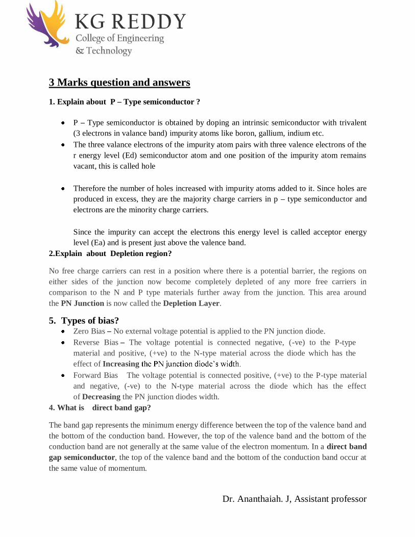
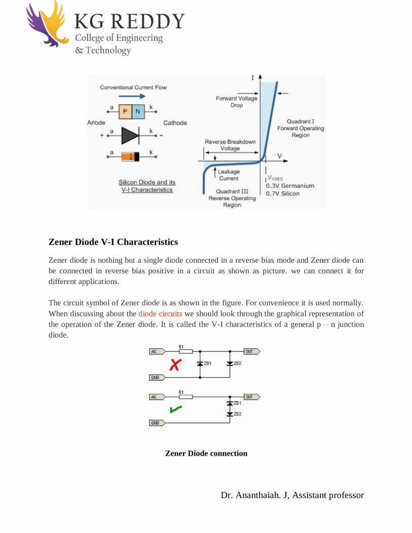
Zener Diode V-I Characteristics
Zener diode is nothing but a single diode connected in a reverse bias mode and Zener diode can be connected in reverse bias positive in a circuit as shown as picture. we can connect it for different applications. The circuit symbol of Zener diode is as shown in the figure. For convenience it is used normally. When discussing about the diode circuits we should look through the graphical representation of the operation of the Zener diode. It is called the V-I characteristics of a general p n junction diode.
Zener Diode connection

Dr. Ananthaiah. J, Assistant professor
Characteristics of a Zener Diode The above diagram shows the V-I characteristics of the Zener diode behavior. When the diode is
connected in forward bias diode acts as a normal diode. When the reverse bias voltage is greater
than a predetermined voltage then the Zener breakdown voltage occurs. To get breakdown
voltage sharp and distinct doping is controlled and the surface imperfections are avoided. In the
V-I characteristics above Vz is the Zener voltage. And also the knee voltage because at this point
the current is the current is very rapid.
Objective question and answers
1. In an intrinsic semiconductor, the Fermi level
a. Lies at the center of forbidden energy gap. b. Is near the conduction band.
c. Is near the valence band. d. May be anywhere in the forbidden energy gap.
2. The ratio of impurity atoms to intrinsic semiconductor atoms in an extrinsic semiconductor is about.
Dr. Ananthaiah. J, Assistant professor
a. 1:10 b. 1:103 c. 1:105 d. 1:108
3. Most commonly used semiconductor material is
a. Silicon b. Germanium c. Mixture of silicon and germanium d. None of the above.
4. At room temperature a semiconductor material is
a. Perfect insulator b. Conductor c. Slightly conducting d. Any one of the above.
5. For silicon, the energy gap at 300 K is
a. 1.1 W b. 1.1 J s c. 1.1 eV d. None of these
6. The forbidden gap for germanium is,
a. 0.12 eV b. 0.72 eV c. 7.2 eV d . None of these
7. The process of adding impurities to a pure semiconductor is called
a. Mixing b. Doping c. Diffusing d. None of the above
8. The pentavalent impurities like antimony, arsenic, bismuth and phosphorus, added to intrinsic semiconductors are called
a. Acceptor or P-type impurities b. Donor or P-type impurities c. Acceptor or N-type impurities d. Donor or N-type impurities
9. Impurities like boron, aluminum, gallium or indium are added to intrinsic semiconductor to form
a. N-type doped semiconductor b. P-type doped c. Junction diode d. All of these
10. a. Germanium b. Silicon c. Carbon d. Sulphur
Dr. Ananthaiah. J, Assistant professor
Fill in the blanks question with answers
1. A semiconductor has generally valence electrons.
2. The resistivity of pure germanium under standard conditions is about
3. The resistivity of a pure silicon is about
4. When a pure semiconductor is heated, its resistance
5. The strength of a semiconductor crystal comes from
6. When a pentavalent impurity is added to a pure semiconductor, it becomes
7. A pentavalent impurity has Valence electron
8. An n-type semiconductor is 9. A hole and electron in close proximity would tend to 10. A reverse bias pn junction has
Answers:- 1.c 2.a 3.a 4.b 5.c 6.b 7.b 8.a 9.a 10.b
1. 4 2. 3. 4. Goes down 5. Electron pair bond 6. n type semiconductor 7.5 8. Electrically neutral 9. Attract each other 10. Almost no current
Dr. Ananthaiah. J, Assistant professor
Unit -III
Optoelectronics
2 Marks question and answers
1. What is radiative ? In physics, radiation is the emission or transmission of energy in the form of waves or particles through space or through a material medium.
2. What is the full form of LED? Light emitting diode
3. Principle of Solar cell? Solar cell, also called photovoltaic cell, any device that directly converts the energy of light into electrical energy through the photovoltaic effect.
4. What is light emission of semiconductor laser? A semiconductor laser (LD) is a device that causes laser oscillation by flowing an electric current to semiconductor.The mechanism of light emission is the same as a light-emitting diode (LED). Light is generated by flowing the forward current to a p-n junction.
5. What is non radiative ? Non-radiative recombination is a process in phosphors and semiconductors, whereby charge carriers recombine without releasing photons. A phonon is released instead. Non-radiative recombination in optoelectronics and phosphors is an unwanted process, lowering the light generation efficiency and increasing heat losses.
3 Marks question and answers
1. Working Principle of Solar Cell or Photovoltaic Cell Conversion of light energy in electrical energy is based on a phenomenon called photovoltaic effect. When semiconductor materials are exposed to light, the some of the photons of light ray are absorbed by the semiconductor crystal which causes a significant number of free electrons in the crystal. This is the basic reason for producing electricity due to photovoltaic effect. Photovoltaic cell is the basic unit of the system where the photovoltaic effect is utilised to
Dr. Ananthaiah. J, Assistant professor
produce electricity from light energy. Silicon is the most widely used semiconductor material for constructing the photovoltaic cell.
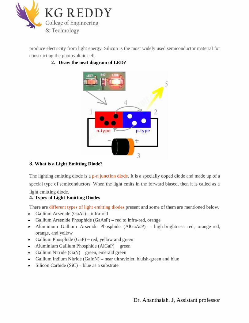
2. Draw the neat diagram of LED?
3. What is a Light Emitting Diode?
The lighting emitting diode is a p-n junction diode. It is a specially doped diode and made up of a special type of semiconductors. When the light emits in the forward biased, then it is called as a light emitting diode. 4. Types of Light Emitting Diodes There are different types of light emitting diodes present and some of them are mentioned below. Gallium Arsenide (GaAs) infra-red Gallium Arsenide Phosphide (GaAsP) red to infra-red, orange Aluminium Gallium Arsenide Phosphide (AlGaAsP) high-brightness red, orange-red,
orange, and yellow Gallium Phosphide (GaP) red, yellow and green Aluminium Gallium Phosphide (AlGaP) green Gallium Nitride (GaN) green, emerald green Gallium Indium Nitride (GaInN) near ultraviolet, bluish-green and blue Silicon Carbide (SiC) blue as a substrate

Dr. Ananthaiah. J, Assistant professor
and they are tiny. The intensity of the LED differs with the help of the microcontroller. 5 Marks question and answers
1. Explain the Working principle of solar cell with neat diagram?
Conversion of light energy in electrical energy is based on a phenomenon called
photovoltaic effect. When materials are exposed to light, the some of the photons of light ray are absorbed by
the semiconductor crystal which causes a significant number of free electrons in the crystal.
This is the basic reason for producing electricity due to photovoltaic effect. Photovoltaic cell is the basic unit of the system where the photovoltaic effect is utilised to produce electricity from light energy.
Silicon is the most widely used semiconductor material for constructing the photovoltaic cell.
The silicon atom has four valence electrons. In a solid crystal, each silicon atom shares each of its four valence electrons with another
nearest silicon atom hence creating covalent bonds between them. In this way, silicon crystal gets a tetrahedral lattice structure. While light ray strikes on any materials some portion of the light is reflected, some
portion is transmitted through the materials and rest is absorbed by the materials.
2. Explain the working principle of LED? The working principle of the Light emitting diode is based on the quantum theory. The quantum theory says that when the electron comes down from the higher energy level to the lower energy level then, the energy emits from the photon. The photon energy is equal to the energy gap between these two energy levels. If the PN-junction diode is in the forward biased, then the current flows through the diode.
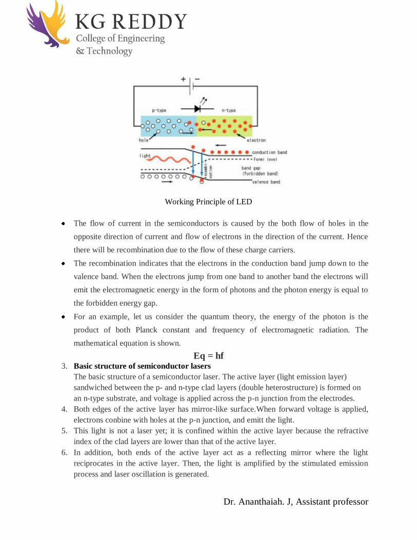
Dr. Ananthaiah. J, Assistant professor
Working Principle of LED
The flow of current in the semiconductors is caused by the both flow of holes in the opposite direction of current and flow of electrons in the direction of the current. Hence there will be recombination due to the flow of these charge carriers.
The recombination indicates that the electrons in the conduction band jump down to the valence band. When the electrons jump from one band to another band the electrons will emit the electromagnetic energy in the form of photons and the photon energy is equal to the forbidden energy gap.
For an example, let us consider the quantum theory, the energy of the photon is the product of both Planck constant and frequency of electromagnetic radiation. The mathematical equation is shown.
Eq = hf 3. Basic structure of semiconductor lasers
The basic structure of a semiconductor laser. The active layer (light emission layer) sandwiched between the p- and n-type clad layers (double heterostructure) is formed on an n-type substrate, and voltage is applied across the p-n junction from the electrodes.
4. Both edges of the active layer has mirror-like surface.When forward voltage is applied, electrons conbine with holes at the p-n junction, and emitt the light.
5. This light is not a laser yet; it is confined within the active layer because the refractive index of the clad layers are lower than that of the active layer.
6. In addition, both ends of the active layer act as a reflecting mirror where the light reciprocates in the active layer. Then, the light is amplified by the stimulated emission process and laser oscillation is generated.

Dr. Ananthaiah. J, Assistant professor
3. I-V Characteristics of LED
There are different types of light emitting diodes are available in the market and there are different LED characteristics which include the color light, or wavelength radiation, light intensity. The important characteristic of the LED is color. In the starting use of LED, there is the only red color. As the use of LED is increased with the help of the semiconductor process and doing the research on the new metals for LED, the different colors were formed.
I-V Characteristics of LED
The following graph shows the approximate curves between the forward voltage and the current. Each curve in the graph indicates the different color. The table shows the summary of the LED characteristics.
4. Explain about Avalanche Effect?
Avalanche effect, in physics, a sudden increase in the flow of an electrical current through a nonconducting or semiconducting solid when a sufficiently strong electrical force is applied.
The ability of most nonmetallic solids to carry an ordinary electrical current is limited by
the scarcity of electrons free to move in the presence of an externally applied electric field.
Dr. Ananthaiah. J, Assistant professor
A sufficiently strong electrical force can break free a large number of electrons from the atoms that form the structure of the solid so that a large current can flow through the material.
This avalanche effect is responsible for the phenomenon of breakdown in insulators and in semiconductors, where it is called the Zener effect.
Because avalanche requires a specific electrical force for each type of substance, it can be used for precise control of voltages in electrical circuits, as in a device called the Zener diode.
At room temperature, even an insulator has a few free electrons. Strong electrical forces cause these electrons to move through the solid rapidly and, if the free electron is moving rapidly enough, it may knock an electron away from an atom in the solid.
This ejected electron (referred to as excited) can move freely through the solid and excite other electrons in the same way, in a process resembling an avalanche in which each rolling rock frees others.
When the electrical force is removed, the newly freed electrons are recaptured by the atoms of the solid, which once again becomes a poor conductor of electricity. Such sudden, large currents may alter or even melt the solid.
Objective question and answers
1. Early LEDs were built up of semiconductor
A. Si B. SiO C. GaAs D. Be
2. GaP were used as light emitter ro achie Ve pale
A. red light B. yellow light C. green light D. blue light
3. GaAs LED emits
A. microwaves B. IR radiations

Dr. Ananthaiah. J, Assistant professor
C. Ultra Violet D. X-rays
4. Light color and Visibility is determined in LED by
A. microwave B. wavelength C. spectrum D. capacitance
5. A common display device of LED is
A. se Ven segment display B. red light pointer C. LED T V D. multilight pointer
6. PIN diode consist of
A. 2 operating regions B. 3 operating regions C. 4 operating regions D. 5 operating regions
7. Whenreverse biased, PIN diode acts as
A. Variable resistor B. constant capacitor C. current controlled switch D. current controlled variable regulator
8. In PIN diode, low forward resistance of intrinsic region decreases when current-
A. increases B. decreases C. become constant D. become infinite
Dr. Ananthaiah. J, Assistant professor
9. When forward biased, PIN diode acts like a
A. constant capacitor B. Variable resistor C. current controlled Variable regulator D. current controlled switch
10. DC beta is the transistor's DC
A. voltage gain B. current gain C. resistor gain D. power gain
Fill in the blanks question with answers 1. Optical fibers uses the ______portion of EM spectrum--
2. Monolithic integration for optical sources are confined to the use of __________ semiconductors-------
3. Circuits fabricated from GaAs or AlGaAs operate in wavelength region of __________
4. P-I-N photoreceiver based on HEMT is integrated with _________ guiding layers.
5. The use of intelligent optical switches is necessary. State whether the given statement is true or false.----------
6. Multilevel interconnections are incorporated in _______
7. Compositional and structural differences between photonic and electronic devices __________
8. The wafer scale replication technology uses ____________
9. Measurement of Hall coefficient enables the determination of------
10. Whenreverse biased, PIN diode acts as-------- constant capacitor.

Dr. Ananthaiah. J, Assistant professor
Answers:-1. c 2. c 3. c 4. b 5. a 6. b 7. b 8. c 9. a 10.a 1. IR 2. III-V 3. 0.8 TO 0.9 µM 4. in GaASP 5. True 6. PIC 7. Create problems 8. SOL gel 9.Conductivity 10. constant capacitor
Dr. Ananthaiah. J, Assistant professor
UNIT-IV
Laser& Fibre Optics
1). What is the full form of LASER?
Light amplification by stimulated emission of radiation.
2). How many types of lasers?
Ruby laser He-Ne laser Semiconductor laser 3). What is Acceptance angle?
The maximum angle of incidence at the end face of an Optical fiber for which the light ray can be propagated along Core-Cladding interface is known as maximum Acceptance angle.
4). What is Numerical Aperture?
The light gathering capacity of an optical fiber is known as Numerical Aperture and it is proportional to Acceptance Angle.
5). What is attenuation?
Attenuation is defined as the reduction in the signal strength or power when it is transmitted (or
guided) through an optical fiber.
3 marks questions with answers
1). What are the characteristics of Laser?
Characteristics of Lasers:
LASER, when compared with any conventional light (Sun light or tube light etc.), Laser posses few outstanding characteristics. 1). Monochromatic: The light emitted from a laser is monochromatic.

Dr. Ananthaiah. J, Assistant professor
2). Directionality:
3). Intensity: The laser light is more intense than conventional light. 2). Applications of Ruby laser?
Laser metal working systems for drilling holes in hard materials. High-power systems for frequency doubling into the UV spectrum. High-brightness holographic camera systems with long coherent length. Medical laser systems for tattoo removal and cosmetic dermatology.
3). Principle of optical fiber &construction? The optical fiber mainly consists of the following six parts.

Dr. Ananthaiah. J, Assistant professor
i) Core ii) Cladding iii) Silicon coating iv) Buffer Jacket v) Strength members vi) Outer jacket.
4). Explain about Acceptance cone?
Rotating the Acceptance angle about the fiber axis
describes the Acceptance Cone of the fiber.
Light launched at the fiber end within this Acceptance
Cone alone will be accepted and propagated to the other end of the
fiber by total internal reflection.
5). Explain about Step Index Fiber?
The refractive index of the core medium is uniform throughout and undergoes an abrupt change
at the interface of the core and cladding. Since the index profile is in the form of a step, these
fibers are called step index fibers. The diameter of the core is about 50 200µm for multimode

Dr. Ananthaiah. J, Assistant professor
and 8 10µm for single mode fibers. The shape of the propagation appears in a zig zag
manner.
5. marks questions with answers
1). Derive the relation between the probabilities of spontaneous emission and stimulated
Consider two energy levels of an atomic system E1 and E2 respectively such that E2 > E1.
Let N1 and N2 be the number of atoms per unit volume present at the levels E1 and E2
respectively and energy density radiation is E2-E1= nhv= (v).
Stimulated Absorption:
Stimulated Absorption rate is proportional to incident energy density (v) of the radiation
incident on the atom and N1.
Therefore, N1P12 (v) N1

Dr. Ananthaiah. J, Assistant professor
N1P12 = B12 (v) N1 ---------(1)
Where B12 is proportional constant, represents property of energy states and is known as
Spontaneous Emission:
Spontaneous Emission rate is proportional to N2 and which is independent of energy
density (v).
Therefore, N2P21 N2
(N2P21)Spont= A21N2 --------(2)
Where A21 is proportional constant, represents property of energy states and is known
Stimulated Emission:
Stimulated Emission rate is proportional to Stimulated energy density (v) of the radiation
incident on the atom and N2.
Therefore, N2P21 (v) N2
(N2P21)Stimu= B21 (v) N2 ------(3)
Where B21 is proportional constant, represents property of energy states and is known as
The total transition probability of atoms from state2 to state1 can be written as
N2P21= (N2P21)Spont + (N2P21)Stimu
N2P21 = N1P12= N2P21
A21N2 + B21 (v) N2 ------(4)
At equilibrium temperature, the number of transitions from state1 to

Dr. Ananthaiah. J, Assistant professor
state2 (Upward transition) will be equal to the number of transitions from
state2 to state1(Downward transition).
Therefore, From eqn(1)&(4),
Comparing equations (7) & (8), we get
coefficients.
2. Explain the working principle of a ruby laser
A ruby laser is a solid-state laser that uses a syntheticruby crystal as its gain medium. The first
working laserwas a ruby laser made by Theodore H. "Ted" Maiman at Hughes Research
Laboratories on May 16, 1960.
Construction:
Ruby is a crystal of aluminium oxide (Al2O3) in which some of the aluminium ions (Al3+) are
replaced by chromium ions (Cr3+). This is done by doping small amounts of chromium oxide
(Cr2O3) in the melt of purified Al2O3.
These chromium ions give the crystal a pink or red color depending upon the concentration of
chromium ions. Laser rods are prepared from a single crystal of pink ruby which contains 0.05%
(by weight) chromium. Al2O3 does not participate in the laser action. It only acts as the host.

Dr. Ananthaiah. J, Assistant professor
The ruby crystal is in the form of cylinder. Length of ruby crystal is usually 2 cm to 30 cm and
diameter 0.5 cm to 2 cm. As very high temperature is produced during the operation of the laser,
the rod is surrounded by liquid nitrogen to cool the apparatus.
Active medium or active center: Chromium ions act as active centers in ruby crystal. So it is
the chromium ions that produce the laser.
Pumping source: A helical flash lamp filled with xenon is used as a pumping source. The ruby
crystal is placed inside a xenon flash lamp. Thus, optical pumping is used to achieve population
inversion in ruby laser.
Optical resonator system: The ends of ruby crystal are polished, grounded and made flat. The
one of the ends is completely silvered while the other one is partially silvered to get the output.
Thus the two polished ends act as optical resonator system.
Ruby is a three level laser system. Suppose there are three levels E1, E2 and (E3 & E4). E1 is the
ground level, E2 is the metastable level, E3 and E4 are the bands. E3 & E4 are considered as
only one level because they are very closed to each other.

Dr. Ananthaiah. J, Assistant professor
Pumping: The ruby crystal is placed inside a xenon flash lamp and the flash lamp is connected
to a capacitor which discharges a few thousand joules of energy in a few milliseconds. A part of
this energy is absorbed by chromium ions in the ground state. Thus optical pumping raises the
chromium ions to energy levels inside the bands E3 and E4. This process is called stimulated
absorption. The transition to bands E3 and E4 are caused by absorption of radiations.
3. Explain the step index and graded index optical fibers.
Step index optical fibers:
The refractive index of the core medium is uniform throughout and undergoes an
abrupt change at the interface of the core and cladding.
Since the index profile is in the form of a step, these fibers are called step index
fibers
The diameter of the core is about 50 200µm for multimode and 8 10µm for single
mode fibers.
The transmitted optical signal is in the form of meridional rays.
The shape of the propagation appears in a zig zag manner.

Dr. Ananthaiah. J, Assistant professor
Graded index optical fibers:
The refractive index of the core medium is made to vary parabolic manner such that the
maximum refractive index present at the center of the core and minimum at core
cladding interface.
Refractive index gradually falls with increase of radius and at the core cladding
interface matches with the refractive index of the cladding.
The variation of refractive index of the core(n) with radius(x) measured from the center
of the core is given above figure.
The transmitted optical signal is in the form of skew or helical rays. 4. Applications of optical fibers
Fiber Optic Sensors:
The measurement techniques developed using fibers are more sensitive and reliable. A smoke
detector and pollution detector can be made from fibersThe high sensitivity of fiber to external
influences, like phase sensitivity, micro-bending losses and modal noise is utilized to develop
new sensors.
There are two types of fiber optic sensors.
1) Intrinsic or active sensors
2) Extrinsic or passive sensor
5. Explain Attenuation in optical fibers
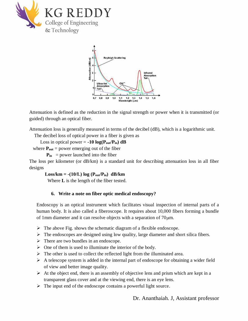
Dr. Ananthaiah. J, Assistant professor
Attenuation is defined as the reduction in the signal strength or power when it is transmitted (or guided) through an optical fiber.
Attenuation loss is generally measured in terms of the decibel (dB), which is a logarithmic unit. The decibel loss of optical power in a fiber is given as Loss in optical power = -10 log(Pout/Pin) dB where Pout = power emerging out of the fiber Pin = power launched into the fiber The loss per kilometer (or dB/km) is a standard unit for describing attenuation loss in all fiber designs Loss/km = -(10/L) log (Pout/Pin) dB/km Where L is the length of the fiber tested.
6. Write a note on fiber optic medical endoscopy?
Endoscopy is an optical instrument which facilitates visual inspection of internal parts of a human body. It is also called a fiberoscope. It requires about 10,000 fibers forming a bundle of 1mm diameter and it can resolve objects with a separation of 70 m.
The above Fig. shows the schematic diagram of a flexible endoscope. The endoscopes are designed using low quality, large diameter and short silica fibers. There are two bundles in an endoscope. One of them is used to illuminate the interior of the body. The other is used to collect the reflected light from the illuminated area. A telescope system is added in the internal part of endoscope for obtaining a wider field
of view and better image quality. At the object end, there is an assembly of objective lens and prism which are kept in a
transparent glass cover and at the viewing end, there is an eye lens. The input end of the endoscope contains a powerful light source.

Dr. Ananthaiah. J, Assistant professor
Objective question and answers
1. Principle of laser is
(a) spontaneous absorption (b) simulated emission
(c) induced emission (d) both b and c 2. Refraction results from differences in light's (a) frequency. (b)amplitude. (c)speed. (d)all of these. (e)none of these. 3. Quantity which does not changes during refraction is (a) direction (b)speed (c)frequency (d) wavelength
4. Bending of light as it passes from one medium to another is called
(a)reflection (b)diffraction (c)refraction (d) deflection
5. Refractive index of a medium is
(a) Speed of light in air to speed of light in vacuum
(b) Speed of light in vacuum to speed of light in air
(c) focal length to object distance
(d) speed of light in the medium x speed of light in the air 6. In the structure of fiber, the light is guided through the core due to total internal
(a) reflection (b) refraction (c) diffraction (d) dispersion 7. Which rays exhibit the variation in the light acceptability ability of the fiber? (a) Meridional (b) Skew (c) Leaky (d) All of the above 8. Which kind of dispersion phenomenon gives rise to pulse spreading in single mode fibers? (a) Intramodal (b) Intermodal (c) Material (d) Group Velocity

Dr. Ananthaiah. J, Assistant professor
9. Which component of fiber optic connector has a provision of entry for the fiber along with the fixation to connector housing. (a) Ferrule (b) Cable (c) Connector housing (d) Coupling Device 10. Which among the following is/are responsible for generating attenuation of an optical power in fiber? (a) Absorption (b) Scattering (c) Waveguide effect (d) All of the above Fill in the blanks question with answers
1. The number of TV channels that can be accommodated using laser is----------------------
2. In Ruby laser the atoms are excited by--------------------------
3. The process of population inversion is to increase the number of atoms in the--------------
4. Laser can be used in the------------------
5. Laser light is intense because------------------------
6. In an optical fiber communication system, which among the following is not a typical
transmitter function--------
7. In single-mode fibers, how does the fraction of energy traveling through bound mode appear
in the cladding?----------------
8. In an optical fiber, the concept of Numerical aperture is applicable in describing the ability of
__________
9. By using Springroove splicing technique, what is the value of mean insertion loss for multi
mode graded index fiber?-----------------
10. In the structure of fiber, the light is guided through the core due to total internal ______
Answers:- 1.b 2.b 3.c 4.b 5.b 6.c 7.a 8.d 9.c 10.a
1.semiconductor laser 2.higher energy state 3.metastable state 4.medical
Dr. Ananthaiah. J, Assistant professor
UNIT-V
Electromagnetism and Magnetic Properties of Materials
2.marks questions with answers
1. Define permi ability?
In electromagnetism, permeability is the measure of the ability of a material to support the formation of a magnetic field within itself. Hence, it is the degree of magnetization that a material obtains in response to an applied magnetic flied.
1. Define Magnetism? Depending on the existence and alignment of magnetic moments with or without application of magnetic field, three types of magnetism can be defined.
2. Define Magnetisation ? With the application of a magnetic field magnetic moments in a material tend to align and thus increase the magnitude of the field strength. This increase is given by the parameter called magnetization, oM. oH + M, such that B = mH. M = m is called magnetic susceptibility. r 1 m =
3. Define magnetic momentum? Magnetic moments Being a moving charge, electrons produce a small magnetic field having a magnetic moment along the axis of rotation. The spin of electrons also produces a magnetic moment along the spin axis. Magnetism in a material arises due to alignment of magnetic moments.
4. Define Super conductivity?
A property of some materials in which their electrical resistance drops tozero, and they acquire th
e ability to carry electric current with no loss ofenergy whatsoever. Formerly, materials develope
d superconductivity onlyat temperatures nearabsolute
zero, but new materials have been foundthat remain superconductive at temperatures above those
of liquidnitrogen. The goal of current research is to find a material that remainssuperconductive
at room temperature.

Dr. Ananthaiah. J, Assistant professor
3 marks questions with answers
1. Explain Magnetic dipole? Analogous to electric dipole, a magnetic dipole can be defined as two monopoles of
opposite and equal strength separated by a certain distance. A magnetic monopole, however, is not observed in nature. If there are
dipole moment can be defined as a vector, Two monopoles of strength +m and m separated by
opposite and equal poles at its two ends.
2. Explain Magnetic field and strength? Magnetic field Strength If a magnetic field, H, is generated by a cylindrical coil
(solenoid) of n turns and length l, H = nI/l (A/m) Magnetic flux density, B: It is the magnitude of the field.
strength within a substance subjected to a field H B = H (Tesla or Weber/m 2 ) , called the permeability, is the measure of the degree to which a material can be magnetized.
In vacuum B = o o is the permeability of vacuum and is a H. universal constant. o = 4 x 10⁻⁷(H/m). r = o is the relative / permeability
3. Explain the Electric polarization? Electric polarization: slight relative shift of positive and negative electric charge in opposite directions within an insulator, or dielectric, induced by an external electric field. Polarization occurs when an electric field distorts the negative cloud of electrons around positive atomic nuclei in a direction opposite the field.
This slight separation of charge makes one side of the atom somewhat positive and the opposite side somewhat negative.
In some materials whose molecules are permanently polarized by chemical forces, such as water molecules, some of the polarization is caused by molecules rotating into the same alignment under the influence of the electric field.
One of the measures of polarization is electric dipole moment, which equals the distance between the slightly shifted centres of positive and negative charge multiplied by the amount of one of the charges.
Polarization P in its quantitative meaning is the amount of dipole moment p per unit volume V of a polarized material, P = p/V.]
Dr. Ananthaiah. J, Assistant professor
4. Derive the relation for Clausius Mossotti's equation?
It gives the relation between the dielectric constant and the ionic polarizability of atoms in dielectric material. If there are N number of atoms, the dipole moment per unit volume which is called Polarization is given by,
we know internal field
From above equations
we know polarization from the relation between polarization and dielectric constant
from the above two equations we get,
Dr. Ananthaiah. J, Assistant professor
5. Explain the piezoelectricity? Piezoelectricity, also called the piezoelectric effect, is the ability of certain materials to generate an AC (alternating current) voltage when subjected to mechanical stress or vibration, or to vibrate when subjected to an AC voltage, or both. The most common piezoelectric material is quartz. Certain ceramics, Rochelle salts, and various other solids also exhibit this effect.
A piezoelectric transducer comprises a "crystal" sandwiched between two metal plates. When a sound wave strikes one or both of the plates, the plates vibrate.
The crystal picks up this vibration, which it translates into a weak AC voltage. Therefore, an AC voltage arises between the two metal plates, with a waveform similar to
that of the sound waves. Conversely, if an AC signal is applied to the plates, it causes the crystal to vibrate in sync
with the signal voltage. As a result, the metal plates vibrate also, producing an acoustic disturbance.
Piezoelectric transducers are common in ultrasonic applications, such as intrusion detectors and alarms. Piezoelectric devices are employed at AF (audio frequencies) as pickups, microphones, earphones, beepers, and buzzers. In wireless applications, piezoelectricity makes it possible to use crystals and ceramics as oscillators that generate predictable and stable signals at RF (radio frequencies).
5 marks questions with answers
1. Explain types of magnetism?
Types of Magnetism
gnetically characterized based on the way it can be magnetized.
its magnitude and sign.
-magnetism
-magnetism

Dr. Ananthaiah. J, Assistant professor
-magnetism.
Anti-ferro-magnetism and ferri-magnetisms are considered as subclasses of ferro-magnetism.
Dia-magnetism
-permanent.
ting electrons,
and creates small magnetic dipoles within atoms which oppose the applied field. This action
produces a negative magnetic effect known as diamagnetism.
to the
direction of applied field (H).
in order of -10-5.
-
magnetism
-up with the field, resulting in a
positive magnetization. However, the dipoles do not interact.
a magnetic
field are called para-magnetic, and the effect is termed as para-magnetism.
leading to no net magnetization.
les line-up with the field, resulting in a positive
magnetization.
align all of the dipoles.
Dr. Ananthaiah. J, Assistant professor
s removed.
temperature decreases the paramagnetic effect.
-magnetism is produced in many materials like aluminium, calcium, titanium, alloys of
copper.
agnetic susceptibility of these materials is slightly positive, and lies in the range +10-5 to
+10-2. Ferro-magnetism
- and para- magnetic materials are considered as non-magnetic because they exhibit
magnetization only in presence of an external field.
field.
-up with the imposed magnetic field due to the exchange
interaction or mutual reinforcement of the dipoles. These are chrematistics of ferromagnetism.
-magnetism (Examples: Fe, Co, Ni, Gd) possess magnetic susceptibilities
approaching 106
ature, ferro-magnetic materials behave as para-magnetic materials and
their susceptibility is given by the Curie-
material constant, T temperature, Tc Curie temperature.

Dr. Ananthaiah. J, Assistant professor
2. Explaine hysteresis curve based on domain theory?
Magnetic domains
by the structure of the magnetic dipoles in regions called domains.
moments that are aligned, giving rise to a permanent net
magnetic moment per domain.
Boundaries, also called Bolch walls, are narrow zones in which the direction of the magnetic
moment gradually and continuously changes from that of one domain to that of the next.
nm thick. For a polycrystalline specimen, each grain may have more than one microscopic sized
domain.
random orientation. This type of arrangement represents the lowest free energy.
-magnetized, the net magnetization of these domains is zero,
because adjacent domains may be orientated randomly in any number of directions, effectively
canceling each other out.
on of a ferro-magnetic material is intimately related to the
domain structure.
field grow at the expense of unaligned domains. This process continues until only the most
favorably oriented domains remain.
Dr. Ananthaiah. J, Assistant professor
force required for this moment.
ses the
domains to rotate and align parallel to the applied field. At this instant material reaches saturation
magnetization and no further increase will take place on increasing the strength of the external
field.
y of these materials becomes quite small.
Magnetic hysteresis
1. Once magnetic saturation has been achieved, a decrease in the applied field back to zero
results in a macroscopically permanent or residual magnetization, known as remanance, Mr. The
corresponding induction, Br, is called retentivity or remanent induction of the magnetic material.
This effect of retardation by material is called hysteresis.
2. The magnetic field strength needed to bring the induced magnetization to zero is termed as
coercivity, Hc. This must be applied anti-parallel to the original field.
3. A further increase in the field in the opposite direction results in a maximum induction in the
opposite direction. The field can once again be reversed, and the field-magnetization loop can be
closed, this loop is known as hysteresis loop or B-H plot or M- H plot.
3. Explain Meissner effect?
The Meissner effect In 1933, Walter Meissner and Robert Ochsenfeld discovered a
magnetic phenomenon that showed that superconductors are not just perfect conductors.
Figure 3 illustrates a thought experiment that highlights this difference. Imagine that both
the ideal conductor and superconductor are above their critical temperature, Tc.
That is, they both are in a normal conducting state and have electrical resistance. A
magnetic field, Ba, is then applied.
Dr. Ananthaiah. J, Assistant professor
This results in the field penetrating both materials. Both samples are then cooled so that
the ideal conductor now has zero resistance.
It is found that the superconductor expels the magnetic field from inside it, while the
ideal conductor maintains its interior field. Note that energy is needed by the
superconductor to expel the magnetic field.
This energy comes from the exothermic superconducting transition. Switching off the
field induces currents in the ideal conductor that prevent Figure 2.
The critical temperatures of some superconductors. changes in the magnetic field inside it
However, the superconductor returns to its initial state, i.e. no magnetic field inside or
outside it. Type I and II superconductors High magnetic fields destroy superconductivity
and restore the
The procedure below, will guide the experimenter through a demonstration normal.
4. Explain Dielectric constant?
The dielectric constant is the ratio of the permittivity of a substance to the
permittivity of free space. It is an expression of the extent to which a material concentrates
electric flux, and is the electrical equivalent of relative magnetic permeability.
As the dielectric constant increases, the electric flux density increases, if all other
factors remain unchanged. This enables objects of a given size, such as sets of metal plates, to
hold their electric charge for long periods of time, and/or to hold large quantities of charge.
Materials with high dielectric constants are useful in the manufacture of high-value capacitors.
A high dielectric constant, in and of itself, is not necessarily desirable.
Generally, substances with high dielectric constants break down more easily when
subjected to intense electric fields, than do materials with low dielectric constants.
For example, dry air has a low dielectric constant, but it makes an excellent dielectric
material for capacitors used in high-power radio-frequency (RF) transmitters.

Dr. Ananthaiah. J, Assistant professor
Even if air does undergo dielectric breakdown (a condition in which the dielectric
suddenly begins to conduct current), the breakdown is not permanent.
When the excessive electric field is removed, air returns to its normal dielectric state.
Solid dielectric substances such as polyethylene or glass, however, can sustain permanent
damage.
5. Explain the Displacement vector?
In a dielectric material the presence of an electric field E causes the bound charges in the
material (atomic nuclei and their electrons) to slightly separate, inducing a local electric dipole
moment.
where is the vacuum permittivity (also called permittivity of free space), and P is the
(macroscopic) density of the permanent and induced electric dipole moments in the material,
called the polarization density.
The displacement field satisfies Gauss's law in a dielectric:
Separate the total volume charge density into free and bound charges:The density can be
rewritten as a function of the polarization P
:The polarization P is defined to be a vector field whose divergence yields the density of
bound charges b in the material. The electric field satisfies the equation
Electrostatic forces on ions or electrons in the material are governed by the electric
field E in the material via the Lorentz Force. Also, D is not determined exclusively by the
free charge. As E has a curl of zero in electrostatic situations.
The effect of this equation can be seen in the case of an object with a "frozen in" polarization
like a bar electret, the electric analogue to a bar magnet. There is no free charge in such a
material, but the inherent polarization gives rise to an electric field, demonstrating that
the D field is not determined entirely by the free charge. relation along with other boundary
conditions on the polarization density to yield the bound charges, which will, in turn, yield the
electric field.
Dr. Ananthaiah. J, Assistant professor
In a linear, homogeneous, isotropic dielectric with instantaneous response to changes in
the electric field, P depends linearly on the electric field,
where the constant of proportionality is called the electric susceptibility of the material.
where = 0 r is the permittivity, and r = 1 + the relative permittivity of the material.
In linear, homogeneous, isotropic media, is a constant. However, in
linear anisotropic media it is a tensor, and in nonhomogeneous media it is a function of
position inside the medium.
Objective question and answers 1. For diamagnetic material, which of the following is correct?
a) Magnetic susceptibility < 0
b) Magnetic susceptibility > 0
c) Magnetic susceptibility = 0
d) None of the mentioned
2. ect about
diamagnetic material?
a) Relative permeability = 0
b) Relative permeability < 1
c) Relative permeability > 1
d) None of the mentioned
3. Magnetic permeability has units as
(a) Wb / m2
(b) Wb / A.m
(c) A / m
(d) Tesla / m

Dr. Ananthaiah. J, Assistant professor
4.
material?
a) Relative permeability = 0
b) Relative permeability < 1
c) Relative permeability > 1
d) None of the mentioned
6. The superconducting state is perfectly _____ in nature.
a. Diamagnetic
b. Paramagnetic
c. Ferromagnetic
d. Ferromagnetic
7. When an electric field is applied to a nonpolar or polar dielectric material, on
lower surface there exists a net
A. positive charge density B. negative charge density C. neutral charge density D. no charge density
8. bdielectric constant of paraffin is
A. 2.1 B. 1.03 C. 2.22 D. 2.8
9. Dieelectric constant of air is
A. 1.0006 B. 1.03

Dr. Ananthaiah. J, Assistant professor
C. 2.1 D. 2.2
8. In absence of applied electric field in nonpolar dielectric materials, charges are averaged in such a way that
A. opposite charges add each other B. opposite charges cancel each other C. similar charges add each other D. similar charges repel each other
10. Class of dielectric material which exhibit a hysteresis loop of polarization versus electric field is termed as
A. ferroelectrics B. elecrets C. ferrites D. dipole
Fill in the blanks question and answers 1. With increase in temperature magnetic susceptibility of ferromagnetic material._________________.
2. With increase in the area of hysteresis curve, power loss will_________________.
3. Magnetic Bubbles are used as ______________.
4. Example for anti-ferro-magnetic materials_____________.
5. In superconductivity, the electrical resistance of material becomes_____________.
6. Dielectric constant=30 for_________________
7. In conductors, opposite charges are separated by______________
8. Dielectric constant of paraffin is-------

Dr. Ananthaiah. J, Assistant professor
9. Material posses electrical polarization in which absence of an applied field and owing to their structure, possess_______________
10.Electric susceptibility is inversely proportional to------
Answers:-1.a 2.b 3.b 4.c 5.a 6.a 7. a 8.a 9.b 10.a
1. First increases then decreases 2. Increases 3. Storage device
4. salts of transition elements . 5. Zero 6. Gallium Arsenide
7. microscopic distances
8. 2.1 9. permanent dipole moment 10. permitivity

Dr. Ananthaiah. J, Assistant professor
17. Beyond syllabus topics with materials
Topics:
1. Types of coherence?
2. Double diffraction?
1. Types of coherence?
Spatial and Temporal coherence Spatial coherence is a concept of wave disturbance describing the correlation between periodic transmitted energy (wave signals) from one point to another, it can also be said that it is a mutual interdependence or connection of variable wave quantities of two different points in a given instant of time, the coherence is presented as a function of distance and mapped as correlation against an absolute distance between points in question.
While spatial coherence is concerned with the phase correlation of waves in different observation points, temporal coherence entails the phase correlation of waves at a given point in space at two different instances of time, it is the measure of the average correlation between the value of a wave and itself delayed by a certain period of time depicting the characteristics of how well a wave can create an interference with itself. The delay on which the correlation effect is emphatically low is denoted by the degree of Tc (coherence time). a state at which there is a significant shift in amplitude.
3. Double slit Experiment ?
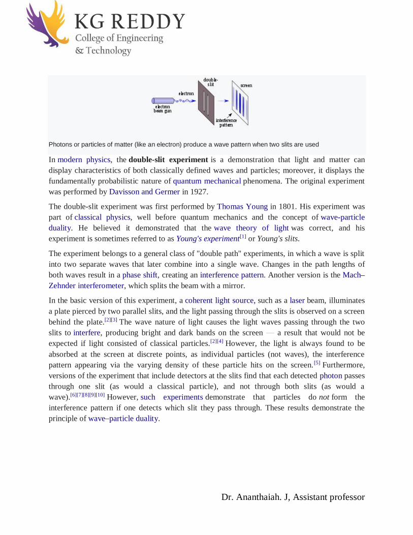
Dr. Ananthaiah. J, Assistant professor
Photons or particles of matter (like an electron) produce a wave pattern when two slits are used
In modern physics, the double-slit experiment is a demonstration that light and matter can display characteristics of both classically defined waves and particles; moreover, it displays the fundamentally probabilistic nature of quantum mechanical phenomena. The original experiment was performed by Davisson and Germer in 1927.
The double-slit experiment was first performed by Thomas Young in 1801. His experiment was part of classical physics, well before quantum mechanics and the concept of wave-particle duality. He believed it demonstrated that the wave theory of light was correct, and his experiment is sometimes referred to as Young's experiment[1] or Young's slits.
The experiment belongs to a general class of "double path" experiments, in which a wave is split into two separate waves that later combine into a single wave. Changes in the path lengths of both waves result in a phase shift, creating an interference pattern. Another version is the MachZehnder interferometer, which splits the beam with a mirror.
In the basic version of this experiment, a coherent light source, such as a laser beam, illuminates a plate pierced by two parallel slits, and the light passing through the slits is observed on a screen behind the plate.[2][3] The wave nature of light causes the light waves passing through the two slits to interfere, producing bright and dark bands on the screen a result that would not be expected if light consisted of classical particles.[2][4] However, the light is always found to be absorbed at the screen at discrete points, as individual particles (not waves), the interference pattern appearing via the varying density of these particle hits on the screen. [5] Furthermore, versions of the experiment that include detectors at the slits find that each detected photon passes through one slit (as would a classical particle), and not through both slits (as would a wave).[6][7][8][9][10] However, such experiments demonstrate that particles do not form the interference pattern if one detects which slit they pass through. These results demonstrate the principle of wave particle duality.

Dr. Ananthaiah. J, Assistant professor


![New E-items Added Title Author Publisher Published ... · Rare earth and transition metal doping of semiconductor materials [electronic resource] : synthesis, magnetic properties](https://img.dokumen.tips/doc/110x75/5f4d2ba8d838840a470eade3/new-e-items-added-title-author-publisher-published-rare-earth-and-transition.jpg)