Embed Size (px)
Citation preview

10 MHz to 10 GHz 67 dB TruPwr Detector
Data Sheet ADL5906
Rev. A Document Feedback Information furnished by Analog Devices is believed to be accurate and reliable. However, no responsibility is assumed by Analog Devices for its use, nor for any infringements of patents or other rights of third parties that may result from its use. Specifications subject to change without notice. No license is granted by implication or otherwise under any patent or patent rights of Analog Devices. Trademarks and registered trademarks are the property of their respective owners.
One Technology Way, P.O. Box 9106, Norwood, MA 02062-9106, U.S.A. Tel: 781.329.4700 ©2013 Analog Devices, Inc. All rights reserved. Technical Support www.analog.com
FEATURES Accurate rms-to-dc conversion from 10 MHz to 10 GHz Single-ended ±1.0 dB dynamic range: 67 dB at 2.14 GHz
No balun or external input matching required Response independent of waveform types, such as
GSM-EDGE/CDMA/W-CDMA/TD-SCDMA/WiMAX/LTE Logarithmic slope: 55 mV/dB Temperature stability: <±1 dB from −40°C to +125°C Operating temperature: −55°C to +125°C Supply voltage: 4.75 V to 5.25 V Sleep current: 250 µA Pin compatible with ADL5902 and AD8363
APPLICATIONS Power amplifier linearization/control loops Transmitter signal strength indication (TSSI) RF instrumentation
FUNCTIONAL BLOCK DIAGRAM
TADJ/PWDN
NIC
VREF VTGT
CRMS
VRMS
VSET
VTEMP
NIC
RFIN–
RFIN+
NIC
GND1GND2
EPAD
X2
BIAS AND POWERDOWN CONTROL
1
ITGT
LINEAR-IN-dB VGA(NEGATIVE SLOPE)
ISQR
26pF
2
VPOS1 VPOS23
411
10
9
5
6
7
8
16
15
14
13
ADL5906
12
X2
VREF2.3V
TEMPERATURESENSOR
G = 5
1128
7-00
1
Figure 1.
GENERAL DESCRIPTION The ADL5906 is a true rms responding power detector that has a 67 dB measurement range when driven with a single-ended 50 Ω source. The easy to use input makes the ADL5906 frequency versatile by eliminating the need for a balun or any other form of external input tuning for operation up to 10 GHz.
The ADL5906 provides a solution in a variety of high frequency systems requiring an accurate rms measurement of signal power. The ADL5906 can operate from 10 MHz to 10 GHz and can accept inputs from −65 dBm to +8 dBm with varying crest factors and bandwidths, such as GSM-EDGE, CDMA, W-CDMA, TD-SCDMA, WiMAX, and OFDM-based LTE carriers. In addition, its temperature stability over the broad temperature range of −55°C to +125°C makes it ideally suited for a wide array of communications, military, industrial, and instrumentation applications.
Used as a power measurement device, VRMS is connected to VSET. The output is then proportional to the logarithm of the rms value of the input. In other words, the reading is presented directly in decibels and is scaled 1.1 V per decade, or 55 mV/dB; other slopes are easily arranged. In controller mode, the voltage applied to VSET determines the power level required at the input to null the deviation from the setpoint. The output buffer can provide high load currents.
Requiring only a single supply of 5 V and a few capacitors, it is easy to use and capable of being driven single-ended or with a balun for differential input drive. The ADL5906 has a low 250 µA sleep current when powered down by a logic high applied to the PWDN pin. It powers up within approximately 1.4 µs to its nominal operating current of 68 mA at 25°C.
The ADL5906 is supplied in a 4 mm × 4 mm, 16-lead LFCSP, and it is pin compatible with the ADL5902 and the AD8363 TruPwr™ rms detectors. This feature allows the designer to create one circuit layout for projects requiring different dynamic ranges. A fully populated RoHS-compliant evaluation board is available.

ADL5906 Data Sheet
Rev. A | Page 2 of 32
TABLE OF CONTENTS Features .............................................................................................. 1 Applications ....................................................................................... 1 Functional Block Diagram .............................................................. 1 General Description ......................................................................... 1 Revision History ............................................................................... 2 Specifications ..................................................................................... 3 Absolute Maximum Ratings ............................................................ 7
ESD Caution .................................................................................. 7 Pin Configuration and Function Descriptions ............................. 8 Typical Performance Characteristics ............................................. 9 Theory of Operation ...................................................................... 16
Square Law Detector and Amplitude Target .............................. 16 RF Input Interface ...................................................................... 17 Temperature Sensor Interface ................................................... 17 VREF Interface ........................................................................... 17 Temperature Compensation Interface ..................................... 18 Power-Down Interface ............................................................... 19
VSET Interface ............................................................................ 19 Output Interface ......................................................................... 19 VTGT Interface .......................................................................... 19 Basis for Error Calculations ...................................................... 20 Measurement Mode Basic Connections.................................. 20 Setting VTADJ ................................................................................ 20 Setting VTGT ................................................................................. 21 Choosing a Value for CRMS ......................................................... 21 Output Voltage Scaling .............................................................. 22 System Calibration and Error Calculation .............................. 24 Using VTEMP to Improve Intercept Temperature Drift ........... 25 Description of Characterization ............................................... 27
Evaluation Board ............................................................................ 28 Evaluation Board Assembly Drawings .................................... 29
Outline Dimensions ....................................................................... 30 Ordering Guide .......................................................................... 30
REVISION HISTORY 10/13—Rev. 0 to Rev. A Changes to Table 2 ............................................................................ 7 Changes to Ordering Guide .......................................................... 30 3/13—Revision 0: Initial Version

Data Sheet ADL5906
Rev. A | Page 3 of 32
SPECIFICATIONS VPOS1 = VPOS2 = 5 V, TA = 25°C, single-ended input drive, RT = 60.4 Ω, VRMS connected to VSET, VTGT = 0.8 V, CRMS = 0.1 µF. Negative current values imply that the ADL5906 is sourcing current out of the indicated pin.
Table 1. Parameter Test Conditions/Comments Min Typ Max Unit OVERALL FUNCTION
Frequency Range 10 to 10,000 MHz RF INPUT INTERFACE RFIN+, Pin RFIN− (Pin 14, Pin 15), ac-coupled
Input Impedance Single-ended drive, 50 MHz 2500 Ω Common-Mode Voltage 2.5 V
100 MHz ±1.0 dB Dynamic Range Continuous wave (CW) input, TA = 25°C 62 dB Maximum Input Level, ±1.0 dB Calibration at −55 dBm, −40 dBm, and 0 dBm 2 dBm Minimum Input Level, ±1.0 dB Calibration at −55 dBm, −40 dBm, and 0 dBm −60 dBm Deviation vs. Temperature Deviation from output at 25°C, VTADJ = 0.35 V −40°C < TA < +85°C; PIN = 0 dBm −0.8/+0.2 dB −40°C < TA < +85°C; PIN = −45 dBm −0.8/+0.4 dB −55°C < TA < +125°C; PIN = 0 dBm −1.3/+0.2 dB −55°C < TA < +125°C; PIN = −45 dBm −1.2/+0.6 dB Logarithmic Slope −65 dBm < PIN < +10 dBm; calibration at −40 dBm and 0 dBm 59 mV/dB Logarithmic Intercept −65 dBm < PIN < +10 dBm; calibration at −40 dBm and 0 dBm −64 dBm
700 MHz ±1.0 dB Dynamic Range CW input, TA = 25°C 62 dB Maximum Input Level, ±1.0 dB Calibration at −55 dBm, −40 dBm, and 0 dBm 2 dBm Minimum Input Level, ±1.0 dB Calibration at −55 dBm, −40 dBm, and 0 dBm −60 dBm Deviation vs. Temperature Deviation from output at 25°C, VTADJ = 0.35 V −40°C < TA < +85°C; PIN = 0 dBm −0.9/+0.3 dB −40°C < TA < +85°C; PIN = −45 dBm −0.9/+0.4 dB −55°C < TA < +125°C; PIN = 0 dBm −1.5/+0.3 dB −55°C < TA < +125°C; PIN = −45 dBm −1.3/+0.7 dB Logarithmic Slope −65 dBm < PIN < +10 dBm; calibration at −40 dBm, and 0 dBm 59 mV/dB Logarithmic Intercept −65 dBm < PIN < +10 dBm; calibration at −40 dBm and 0 dBm −65 dBm
900 MHz ±1.0 dB Dynamic Range CW input, TA = 25°C 63 dB Maximum Input Level, ±1.0 dB Calibration at −55 dBm, −40 dBm, and 0 dBm 3 dBm Minimum Input Level, ±1.0 dB Calibration at −55 dBm, −40 dBm, and 0 dBm −60 dBm Deviation vs. Temperature Deviation from output at 25°C, VTADJ = 0.35 V −40°C < TA < +85°C; PIN = 0 dBm −0.8/+0.3 dB −40°C < TA < +85°C; PIN = −45 dBm −0.9/+0.4 dB −55°C < TA < +125°C; PIN = 0 dBm −1.4/+0.3 dB −55°C < TA < +125°C; PIN = −45 dBm −1.4/+0.8 dB Logarithmic Slope −65 dBm < PIN < +10 dBm; calibration at −40 dBm and 0 dBm 59 mV/dB Logarithmic Intercept −65 dBm < PIN < +10 dBm; calibration at −40 dBm and 0 dBm −65 dBm Deviation from CW Response
(−45 dBm to −5 dBm) 12.16 dB peak-to-rms ratio (four-carrier W-CDMA) −0.1 dB
11.58 dB peak-to-rms ratio (LTE TM1, one-carrier, 20 MHz bandwidth)
−0.2 dB
10.56 dB peak-to-rms ratio (W-CDMA) 0.05 dB 7.4 dB peak-to-rms ratio (64 QAM) −0.1 dB

ADL5906 Data Sheet
Rev. A | Page 4 of 32
Parameter Test Conditions/Comments Min Typ Max Unit 1900 MHz
±1.0 dB Dynamic Range CW input, TA = 25°C 66 dB Maximum Input Level, ±1.0 dB Calibration at −55 dBm, −40 dBm, and 0 dBm 6 dBm Minimum Input Level, ±1.0 dB Calibration at −55 dBm, −40 dBm, and 0 dBm −60 dBm Deviation vs. Temperature Deviation from output at 25°C, VTADJ = 0.35 V −40°C < TA < +85°C; PIN = 0 dBm −0.8/+0.2 dB −40°C < TA < +85°C; PIN = −45 dBm −0.8/+0.5 dB −55°C < TA < +125°C; PIN = 0 dBm −1.4/+0.2 dB −55°C < TA < +125°C; PIN = −45 dBm −1.2/+0.9 dB Logarithmic Slope −65 dBm < PIN < +10 dBm; calibration at −40 dBm and 0 dBm 57 mV/dB Logarithmic Intercept −65 dBm < PIN < +10 dBm; calibration at −40 dBm and 0 dBm −65 dBm
2140 MHz ±1.0 dB Dynamic Range CW input, TA = 25°C 67 dB Maximum Input Level, ±1.0 dB Calibration at −55 dBm, −40 dBm, and 0 dBm 7 dBm Minimum Input Level, ±1.0 dB Calibration at −55 dBm, −40 dBm, and 0 dBm −60 dBm Deviation vs. Temperature Deviation from output at 25°C, VTADJ = 0.35 V −40°C < TA < +85°C; PIN = 0 dBm −0.8/+0.3 dB −40°C < TA < +85°C; PIN = −45 dBm −0.8/+0.6 dB −55°C < TA < +125°C; PIN = 0 dBm −1.3/+0.3 dB −55°C < TA < +125°C; PIN = −45 dBm −1.2/+0.9 dB Logarithmic Slope −65 dBm < PIN < +10 dBm; calibration at −40 dBm and 0 dBm 56 mV/dB Logarithmic Intercept −65 dBm < PIN < +10 dBm; calibration at −40 dBm and 0 dBm −65 dBm Deviation from CW Response
(−45 dBm to −5 dBm) 12.16 dB peak-to-rms ratio (four-carrier W-CDMA) −0.1 dB
11.58 dB peak-to-rms ratio (LTE TM1, one-carrier, 20 MHz bandwidth)
0.1 dB
10.56 dB peak-to-rms ratio (one-carrier W-CDMA) 0.1 dB 7.4 dB peak-to-rms ratio (64 QAM) −0.1 dB
2600 MHz ±1.0 dB Dynamic Range CW input, TA = 25°C 68 dB Maximum Input Level, ±1.0 dB Calibration at −55 dBm, −40 dBm, and 0 dBm 8 dBm Minimum Input Level, ±1.0 dB Calibration at −55 dBm, −40 dBm, and 0 dBm −60 dBm Deviation vs. Temperature Deviation from output at 25°C, VTADJ = 0.4 V −40°C < TA < +85°C; PIN = 0 dBm −0.9/+0.3 dB −40°C < TA < +85°C; PIN = −45 dBm −1/+0.5 dB −55°C < TA < +125°C; PIN = 0 dBm −1.4/+0.3 dB −55°C < TA < +125°C; PIN = −45 dBm −1.4/+0.8 dB Logarithmic Slope −65 dBm < PIN < +10 dBm; calibration at −40 dBm and 0 dBm 55 mV/dB Logarithmic Intercept −65 dBm < PIN < +10 dBm; calibration at −40 dBm and 0 dBm −65 dBm
3500 MHz ±1.0 dB Dynamic Range CW input, TA = 25°C 65 dB Maximum Input Level, ±1.0 dB Calibration at −55 dBm, −40 dBm, and 0 dBm 5 dBm Minimum Input Level, ±1.0 dB Calibration at −55 dBm, −40 dBm, and 0 dBm −60 dBm Deviation vs. Temperature Deviation from output at 25°C, VTADJ = 0.45 V −40°C < TA < +85°C; PIN = 0 dBm −1.5/0 dB −40°C < TA < +85°C; PIN = −45 dBm −1/+0.3 dB −55°C < TA < +125°C; PIN = 0 dBm −1.5/0 dB −55°C < TA < +125°C; PIN = −45 dBm −1.4/+0.4 dB Logarithmic Slope −65 dBm < PIN < +10 dBm; calibration at −40 dBm and 0 dBm 52 mV/dB Logarithmic Intercept −65 dBm < PIN < +10 dBm; calibration at −40 dBm and 0 dBm −64 dBm
Data Sheet ADL5906
Rev. A | Page 5 of 32
Parameter Test Conditions/Comments Min Typ Max Unit 5800 MHz
±1.0 dB Dynamic Range CW input, TA = 25°C 57 dB Maximum Input Level, ±1.0 dB Calibration at −50 dBm, −40 dBm, and 0 dBm 3 dBm Minimum Input Level, ±1.0 dB Calibration at −50 dBm, −40 dBm, and 0 dBm −54 dBm Deviation vs. Temperature Deviation from output at 25°C, VTADJ = 1 V −40°C < TA < +85°C; PIN = 0 dBm −2.4/+0 dB −40°C < TA < +85°C; PIN = −45 dBm −1.4/-0.2 dB −55°C < TA < +125°C; PIN = 0 dBm −3.6/+0 dB −55°C < TA < +125°C; PIN = −45 dBm −2.1/-0.2 dB Logarithmic Slope −65 dBm < PIN < +10 dBm; calibration at −40 dBm and 0 dBm 42 mV/dB Logarithmic Intercept −65 dBm < PIN < +10 dBm; calibration at −40 dBm and 0 dBm −60 dBm
OUTPUT INTERFACE VRMS (Pin 6) Output Swing, Controller Mode Swing range minimum, RL ≥ 500 Ω to ground 0.05 V Swing range maximum, RL ≥ 500 Ω to ground 3.92 V Current Source/Sink Capability 10/10 mA Rise Time PIN = off to −10 dBm, 10% to 90%, CRMS = 1 nF 0.1 µs Fall Time PIN = −10 dBm to off, 90% to 10%, CRMS = 1 nF 14.6 µs
SETPOINT INPUT VSET (Pin 7) Voltage Range Log conformance error ≤ 1 dB, minimum 2.14 GHz 3.92 V Log conformance error ≤ 1 dB, maximum 2.14 GHz 0.4 V Input Resistance 72 kΩ Logarithmic Scale Factor f = 2.14 GHz 56 mV/dB Logarithmic Intercept f = 2.14 GHz −65 dBm
TEMPERATURE COMPENSATION TADJ/PWDN (Pin 1) Input Voltage Range 0 VPOS V Input Bias Current VTADJ = 0.35 V 5 µA Input Resistance VTADJ = 0.35 V 70 kΩ
VOLTAGE REFERENCE VREF (Pin 11) Output Voltage PIN = −55 dBm 2.3 V Temperature Sensitivity 25°C ≤ TA ≤ 125°C −0.12 mV/°C
−55°C ≤ TA ≤ +25°C 0.07 mV/°C Short-Circuit Current Source/
Sink Capability 25°C ≤ TA ≤ 125°C 4/0.05 mA
−55°C ≤ TA ≤ +25°C 3/0.05 mA Voltage Regulation TA = 25°C, ILOAD = 2 mA −0.4 %
TEMPERATURE REFERENCE VTEMP (Pin 8) Output Voltage TA = 25°C, RL ≥ 10 kΩ 1.4 V Temperature Coefficient −40°C ≤ TA ≤ +125°C, RL ≥ 10 kΩ 4.8 mV/°C Short-Circuit Current Source/
Sink Capability 25°C ≤ TA ≤ 125°C 4/0.05 mA
−55°C ≤ TA ≤ +25°C 3/0.05 mA Voltage Regulation TA = 25°C, ILOAD = 1 mA −2.8 %
RMS TARGET INTERFACE VTGT (Pin 12) Input Voltage Range 0.2 2.5 V Input Bias Current VTGT = 0.8 V 8 µA Input Resistance 100 kΩ
POWER-DOWN INTERFACE VTADJ/PWDN (Pin 1) Voltage Level to Enable VPWDN decreasing 1.3 V Voltage Level to Disable VPWDN increasing 1.4 V Input Bias Current VPWDN = 5 V 72 µA VPWDN = 0 V 0.1 µA Enable Time VPWDN low to VRMS, 10% to 90%, CRMS = 1 nF, PIN = 0 dBm 1.4 µs Disable Time VPWDN high to VRMS, 90% to 10%, CRMS = 1 nF, PIN = 0 dBm 1.0 µs

ADL5906 Data Sheet
Rev. A | Page 6 of 32
Parameter Test Conditions/Comments Min Typ Max Unit POWER SUPPLY INTERFACE VPOS1, VPOS2 (Pin 3, Pin 10)
Supply Voltage 4.75 5 5.25 V Quiescent Current TA = 25°C, PIN < −60 dBm 68 mA TA = 125°C, PIN < −60 dBm 86 mA Power-Down Current VPWDN > 1.4 V 250 µA

Data Sheet ADL5906
Rev. A | Page 7 of 32
ABSOLUTE MAXIMUM RATINGS Table 2. Parameter Rating Supply Voltage, VPOS1, VPOS2 5.25 V Input Average RF Power1 21 dBm
Equivalent Voltage, Sine Wave Input 2.51 V p-p Internal Power Dissipation 550 mW θJC
2 10.6°C/W θJB
2 35.3°C/W θJA
2 57.2°C/W ΨJT
2 1.0°C/W ΨJB
2 34°C/W Maximum Junction Temperature 150°C Operating Temperature Range
(ADL5906ACPZN) −40°C to +105°C
Operating Temperature Range (ADL5906SCPZN)
−55°C to +125°C
Storage Temperature Range −65°C to +150°C Lead Temperature (Soldering, 60 sec) 300°C 1 This is for long durations. Excursions above this level, with durations much
less than 1 second, are possible without damage. 2 No airflow with the exposed pad soldered to a 4-layer JEDEC board.
Stresses above those listed under Absolute Maximum Ratings may cause permanent damage to the device. This is a stress rating only; functional operation of the device at these or any other conditions above those indicated in the operational section of this specification is not implied. Exposure to absolute maximum rating conditions for extended periods may affect device reliability.
ESD CAUTION

ADL5906 Data Sheet
Rev. A | Page 8 of 32
PIN CONFIGURATION AND FUNCTION DESCRIPTIONS
PIN 1INDICATOR
NOTES1. NIC = NO INTERNAL CONNECTION. DO NOT CONNECT TO THIS PIN.2. THE EXPOSED PAD REQUIRES A GOOD THERMAL
AND ELECTRICAL CONNECTION TO THE GROUND OF THE PRINTED CIRCUIT BOARD (PCB).
1TADJ/PWDN2NIC3VPOS14GND1
11 VREF12 VTGT
10 VPOS29 GND2
5C
RM
S6
VRM
S7
VSET
8VT
EMP
15R
FIN
–16
NIC
14R
FIN
+13
NIC
TOP VIEW(Not to Scale)
ADL5906
1128
7-00
2
Figure 2. Pin Configuration
Table 3. Pin Function Descriptions Pin No. Mnemonic Description 1 TADJ/PWDN Temperature Compensation/Shutdown. This is a dual function pin used for controlling temperature slope
compensation at voltages <1.0 V and/or for shutting down the device at voltages >1.4 V. The temperature compensation voltage is generally set by connecting this pin to VREF through a resistive voltage divider (see the Setting VTADJ section for additional information). See Figure 46 for an equivalent circuit.
2, 13, 16 NIC No Internal Connection. Do not connect to these pins. These pins are not internally connected. 3, 10 VPOS1,
VPOS2 Power Supply. Because these pins are internally shorted, they must be connected to the same 5 V power supply. The power supply to each pin must also be decoupled using 100 pF and 100 nF capacitors located as close as possible to the pins.
4, 9 GND1, GND2 Ground. Connect both GND1 and GND2 to system ground using a low impedance path. 5 CRMS RMS Averaging Capacitor. Connect an rms averaging capacitor between CRMS and ground. See the Choosing
a Value for CRMS section for more information. See Figure 48 for an equivalent circuit. 6 VRMS RMS Output. In measurement mode, this pin is connected to VSET either directly or through a resistor divider
(when the slope is being increased). In controller mode, this pin is used to drive the gain control input of a voltage variable attenuator (VVA) or variable gain amplifier (VGA). See Figure 48 for an equivalent circuit.
7 VSET Setpoint Input. In measurement mode, this pin is connected to VRMS either directly or through a resistor divider. In controller mode, the voltage applied to this pin sets the decibel value of the required RF input level to balance the automatic power control loop. See Figure 47 for an equivalent circuit.
8 VTEMP Temperature Sensor Output of 1.4 V at 25°C with a Coefficient of 4.8 mV/°C. See Figure 43 for an equivalent circuit. 11 VREF Reference Voltage Output. This voltage reference has a nominal value of 2.3 V. This reference output voltage
can be used to set the voltage to the TADJ/PWDN and VTGT pins. See Figure 44 for an equivalent circuit. 12 VTGT RMS Target Voltage. The voltage applied to this pin sets the target RF input at the output of the VGA that is also the
rms squaring circuit. The recommended voltage for VTGT is 0.8 V. Increasing VTGT above 0.8 V degrades the rms accuracy of the ADL5906. Reducing VTGT below 0.8 V can improve the rms accuracy for signals with very high crest factors; however, it reduces the detection range of the ADL5906. See Figure 49 for an equivalent circuit.
14, 15 RFIN+, RFIN− RF Inputs. The RF inputs are normally applied single-ended with the RF input signal ac-coupled to RFIN+ and RFIN− ac-coupled to ground. See Figure 42 for an equivalent circuit.
EPAD The exposed pad on the underside of the device (EPAD) is also internally connected to ground and requires a good thermal and electrical connection to the ground of the printed circuit board (PCB).

Data Sheet ADL5906
Rev. A | Page 9 of 32
TYPICAL PERFORMANCE CHARACTERISTICS VPOS1 = VPOS2 = 5 V, single-ended input drive, VRMS connected to VSET, VTGT = 0.8 V, CRMS = 0.1 µF, TA = +25°C (green), −55°C (light blue), −40°C (blue), +85°C (red), +105°C (orange), and +125°C (black), where appropriate. Error referred to slope and intercept at indicated calibration points. Input RF signal is a sine wave (CW), unless otherwise indicated.
0
0.5
1.0
1.5
2.0
2.5
3.0
3.5
4.0
–65 –60 –55 –50 –45 –40 –35 –30 –25 –20 –15 –10 –5 0 5 10
OU
TPU
T VO
LTA
GE
(V)
100MHz TO 1GHz
20MHz10MHz
PIN (dBm)
1128
7-00
3
2GHz3GHz4GHz5GHz6GHz7GHz8GHz9GHz
10GHz
Figure 3. Typical VRMS vs. Input Power (dBm) vs. Frequency
(10 MHz to 10 GHz) at 25°C
–6
–5
–4
–3
–2
–1
0
1
2
3
4
5
6
0
0.5
1.0
1.5
2.0
2.5
3.0
3.5
4.0
4.5
5.0
5.5
6.0
–65 –55 –45 –35 –25 –15 –5 5
ERR
OR
(dB
)
OU
TPU
T VO
LTA
GE
(V)
PIN (dBm)
CWQPSK PEP = 3.8dB16 QAM PEP = 6.3dB64 QAM PEP = 7.4dB
1128
7-10
4
Figure 4. Error from CW Linear Reference vs. Signal Modulation (QPSK, 16 QAM, 64 QAM), Frequency = 900 MHz, CRMS = 0.1 µF,
Three Point Calibration at 0 dBm, −40 dBm, and −55 dBm
–6
–5
–4
–3
–2
–1
0
1
2
3
4
5
6
0
0.5
1.0
1.5
2.0
2.5
3.0
3.5
4.0
4.5
5.0
5.5
6.0
–65 –55 –45 –35 –25 –15 –5 5
ERR
OR
(dB
)
OU
TPU
T VO
LTA
GE
(V)
PIN (dBm)
CWCDMA 2000 PEP = 11.02dB1C W-CDMA PEP = 10.56dB4C W-CDMA PEP = 12.08dB
1128
7-00
5
Figure 5. Error from CW Linear Reference vs. Signal Modulation (CDMA 2000,
One-Carrier W-CDMA, Four-Carrier W-CDMA), Frequency = 2.14 GHz, CRMS = 0.1 µF, Three Point Calibration at 0 dBm, −40 dBm, and −55 dBm
–20dBm
0
0.5
1.0
1.5
2.0
2.5
3.0
3.5
4.0
0.01 0.1 1 10
OU
TPU
T VO
LTA
GE
(V)
FREQUENCY (GHz)
–50dBm
–10dBm
0dBm
–30dBm
–40dBm
1128
7-00
6
Figure 6. Typical VRMS vs. Frequency for Six RF Input Levels
–6
–5
–4
–3
–2
–1
0
1
2
3
4
5
6
0
0.5
1.0
1.5
2
2.5
3.0
3.5
4.0
4.5
5.0
5.5
6.0
–65 –55 –45 –35 –25 –15 –5 5
ERR
OR
(dB
)
OU
TPU
T VO
LTA
GE
(V)
PIN (dBm)
CWQPSK PEP = 3.8dB16 QAM PEP = 6.3dB64 QAM PEP = 7.4dB
1128
7-00
7
Figure 7. Error from CW Linear Reference vs. Signal Modulation (QPSK, 16 QAM, 64 QAM), Frequency = 2.14 GHz, CRMS = 0.1 µF,
Three Point Calibration at 0 dBm, −40 dBm, and −55 dBm
–6
–5
–4
–3
–2
–1
0
1
2
3
4
5
6
0
0.5
1.0
1.5
2
2.5
3.0
3.5
4.0
4.5
5.0
5.5
6.0
–65 –55 –45 –35 –25 –15 –5 5
ERR
OR
(dB
)
OU
TPU
T VO
LTA
GE
(V)
PIN (dBm)
CWLTE TM1 1CR 20MHz PEP = 11.58dB
1128
7-00
8
Figure 8. Error from CW Linear Reference vs. Signal Modulation
(LTE TM1 One-Carrier, 20 MHz), Frequency = 2.14 GHz, CRMS = 0.1 µF, Three Point Calibration at 0 dBm, −40 dBm, and −55 dBm

ADL5906 Data Sheet
Rev. A | Page 10 of 32
OU
TPU
T VO
LTA
GE
(V)
–6
–5
–4
–3
–2
–1
0
1
2
3
4
5
6
0
0.5
1.0
1.5
2.0
2.5
3.0
3.5
4.0
4.5
5.0
5.5
6.0
ERR
OR
(dB
)
OU
TPU
T VO
LTA
GE
(V)
PIN (dBm)
VTADJ = 0.35VCALIBRATION AT 0dBm, –40dBm, AND –55dBm
1128
7-00
9–65 –55 –45 –35 –25 –15 –5 5
Figure 9. VRMS and Log Conformance Error vs. Input Level and Temperature at
100 MHz
OU
TPU
T VO
LTA
GE
(V)
–6
–5
–4
–3
–2
–1
0
1
2
3
4
5
6
0
0.5
1.0
1.5
2.0
2.5
3.0
3.5
4.0
4.5
5.0
5.5
6.0
ERR
OR
(dB
)
OU
TPU
T VO
LTA
GE
(V)
PIN (dBm)
VTADJ = 0.35VCALIBRATION AT 0dBm, –40dBm, AND –55dBm
1128
7-01
0–65 –55 –45 –35 –25 –15 –5 5
Figure 10. VRMS and Log Conformance Error vs. Input Level and Temperature
at 700 MHz
–6
–5
–4
–3
–2
–1
0
1
2
3
4
5
6
ERR
OR
(dB
)
OU
TPU
T VO
LTA
GE
(V)
0
0.5
1.0
1.5
2.0
2.5
3.0
3.5
4.0
4.5
5.0
5.5
6.0
OU
TPU
T VO
LTA
GE
(V)
5
PIN (dBm)
VTADJ = 0.35VCALIBRATION AT 0dBm, –40dBm, AND –55dBm
1128
7-01
1–65 –55 –45 –35 –25 –15 –5
Figure 11. VRMS and Log Conformance Error vs. Input Level and Temperature
at 900 MHz
–6
–5
–4
–3
–2
–1
0
1
2
3
4
5
6
ERR
OR
(dB
)
0
0.5
1.0
1.5
2.0
2.5
3.0
3.5
4.0
4.5
5.0
5.5
6.0
–65 –55 –45 –35 –25 –15 –5 5
OU
TPU
T VO
LTA
GE
(V)
PIN (dBm) 1128
7-01
2
VTADJ = 0.35V
Figure 12. Distribution of Log Conformance Error with Respect to VRMS at
25°C vs. Input Level and Temperature at 100 MHz
–6
–5
–4
–3
–2
–1
0
1
2
3
4
5
6
0
0.5
1.0
1.5
2.0
2.5
3.0
3.5
4.0
4.5
5.0
5.5
6.0
–65 –55 –45 –35 –25 –15 –5 5
ERR
OR
(dB
)
OU
TPU
T VO
LTA
GE
(V)
PIN (dBm)
1128
7-01
3
VTADJ = 0.35V
Figure 13. Distribution of Log Conformance Error with Respect to VRMS at
25°C vs. Input Level and Temperature at 700 MHz
OU
TPU
T VO
LTA
GE
(V)
–6
–5
–4
–3
–2
–1
0
1
2
3
4
5
6
0
0.5
1.0
1.5
2.0
2.5
3.0
3.5
4.0
4.5
5.0
5.5
6.0
ERR
OR
(dB
)
–65 –55 –45 –35 –25 –15 –5 5
PIN (dBm) 1128
7-01
4
VTADJ = 0.35V
Figure 14. Distribution of Log Conformance Error with Respect to VRMS at
25°C vs. Input Level and Temperature at 900 MHz
Data Sheet ADL5906
Rev. A | Page 11 of 32
–6
–5
–4
–3
–2
–1
0
1
2
3
4
5
6
ERR
OR
(dB
)
OU
TPU
T VO
LTA
GE
(V)
0
0.5
1.0
1.5
2.0
2.5
3.0
3.5
4.0
4.5
5.0
5.5
6.0
OU
TPU
T VO
LTA
GE
(V)
–65 –55 –45 –35 –25 –15 –5 5
PIN (dBm)
VTADJ = 0.35VCALIBRATION AT 0dBm, –40dBm, AND –55dBm
1128
7-01
5
Figure 15. VRMS and Log Conformance Error vs. Input Level and Temperature
at 1.9 GHz
–6
–5
–4
–3
–2
–1
0
1
2
3
4
5
6ER
RO
R (d
B)
OU
TPU
T VO
LTA
GE
(V)
0
0.5
1.0
1.5
2.0
2.5
3.0
3.5
4.0
4.5
5.0
5.5
6.0
OU
TPU
T VO
LTA
GE
(V)
–65 –55 –45 –35 –25 –15 –5 5
PIN (dBm)
VTADJ = 0.35VCALIBRATION AT 0dBm, –40dBm, AND –55dBm
1128
7-01
6
Figure 16. VRMS and Log Conformance Error vs. Input Level and Temperature
at 2.14 GHz
–6
–5
–4
–3
–2
–1
0
1
2
3
4
5
6
ERR
OR
(dB
)
OU
TPU
T VO
LTA
GE
(V)
0
0.5
1.0
1.5
2.0
2.5
3.0
3.5
4.0
4.5
5.0
5.5
6.0
OU
TPU
T VO
LTA
GE
(V)
–65 –55 –45 –35 –25 –15 –5 5
PIN (dBm)
VTADJ = 0.4VCALIBRATION AT 0dBm, –40dBm, AND –55dBm
1128
7-01
7
Figure 17. VRMS and Log Conformance Error vs. Input Level and Temperature at 2.6 GHz
OU
TPU
T VO
LTA
GE
(V)
–6
–5
–4
–3
–2
–1
0
1
2
3
4
5
6
0
0.5
1.0
1.5
2.0
2.5
3.0
3.5
4.0
4.5
5.0
5.5
6.0
ERR
OR
(dB
)
–65 –55 –45 –35 –25 –15 –5 5
PIN (dBm) 1128
7-01
8
VTADJ = 0.35V
Figure 18. Distribution of Log Conformance Error with Respect to VRMS at 25°C vs. Input Level and Temperature at 1.9 GHz
OU
TPU
T VO
LTA
GE
(V)
–6
–5
–4
–3
–2
–1
0
1
2
3
4
5
6
0
0.5
1.0
1.5
2.0
2.5
3.0
3.5
4.0
4.5
5.0
5.5
6.0
ERR
OR
(dB
)
–65 –55 –45 –35 –25 –15 –5 5
PIN (dBm) 1128
7-01
9
VTADJ = 0.35V
Figure 19. Distribution of Log Conformance Error with Respect to VRMS at 25°C vs. Input Level and Temperature at 2.14 GHz
ERR
OR
(dB
)
OU
TPU
T VO
LTA
GE
(V)
–6
–5
–4
–3
–2
–1
0
1
2
3
4
5
6
0
0.5
1.0
1.5
2.0
2.5
3.0
3.5
4.0
4.5
5.0
5.5
6.0
–65 –55 –45 –35 –25 –15 –5 5
PIN (dBm)
1 128
7-02
0
VTADJ = 0.4V
Figure 20. Distribution of Log Conformance Error with Respect to VRMS at 25°C vs. Input Level and Temperature at 2.6 GHz

ADL5906 Data Sheet
Rev. A | Page 12 of 32
–6
–5
–4
–3
–2
–1
0
1
2
3
4
5
6
ERR
OR
(dB
)
OU
TPU
T VO
LTA
GE
(V)
0
0.5
1.0
1.5
2.0
2.5
3.0
3.5
4.0
4.5
5.0
5.5
6.0
OU
TPU
T VO
LTA
GE
(V)
–65 –55 –45 –35 –25 –15 –5 5
PIN (dBm)
VTADJ = 0.45VCALIBRATION AT 0dBm, –40dBm, AND –55dBm
1128
7-02
1
Figure 21. VRMS and Log Conformance Error vs. Input Level and Temperature at 3.5 GHz
0
0.25
0.50
0.75
1.00
1.25
1.50
1.75
2.00
2.25
2.50
2.75
3.00
–6
–5
–4
–3
–2
–1
0
1
2
3
4
5
6
ERR
OR
(dB
)
OU
TPU
T VO
LTA
GE
(V)
–65 –55 –45 –35 –25 –15 –5 5
PIN (dBm)
VTADJ = 1VCALIBRATION AT 0dBm, –40dBm, AND –50dBm
1128
7-02
2
Figure 22. VRMS and Log Conformance Error vs. Input Level and Temperature
at 5.8 GHz
0
0.25
0.50
0.75
1.00
1.25
1.50
1.75
2.00
2.25
2.50
2.75
3.00
–6
–5
–4
–3
–2
–1
0
1
2
3
4
5
6
ERR
OR
(dB
)
OU
TPU
T VO
LTA
GE
(V)
–45 –35 –25 –15 –5 5
PIN (dBm)
VTADJ = 1VCALIBRATION AT 0dBm, –20dBm, AND –35dBm
1128
7-02
3
Figure 23. VRMS and Log Conformance Error vs. Input Level and Temperature
at 8 GHz
ERR
OR
(dB
)
OU
TPU
T VO
LTA
GE
(V)
–6
–5
–4
–3
–2
–1
0
1
2
3
4
5
6
0
0.5
1.0
1.5
2.0
2.5
3.0
3.5
4.0
4.5
5.0
5.5
6.0
–65 –55 –45 –35 –25 –15 –5 5
PIN (dBm)
1128
7-02
4
VTADJ = 0.45V
Figure 24. Distribution of Log Conformance Error with Respect to VRMS at 25°C vs. Input Level and Temperature at 3.5 GHz
–6
–5
–4
–3
–2
–1
0
1
2
3
4
5
6
0
0.5
1.0
1.5
2.0
2.5
3.0
3.5
4.0
4.5
5.0
5.5
6.0
–60 –50 –40 –30 –20 –10 0 10
ERR
OR
(dB
)
OU
TPU
T VO
LTA
GE
(V)
PIN (dBm)
1128
7-02
5
VTADJ = 1V
Figure 25. Distribution of Log Conformance Error with Respect to VRMS at
25°C vs. Input Level and Temperature at 5.8 GHz
0
0.25
0.50
0.75
1.00
1.25
1.50
1.75
2.00
2.25
2.50
2.75
3.00
–35 –25 –15 –5 5
OU
TPU
T VO
LTA
GE
(V)
PIN (dBm)
–6
–5
–4
–3
–2
–1
0
1
2
3
4
5
6
ERR
OR
(dB
)
VTADJ = 1VCALIBRATION AT 0dBm, –10dBm, AND –20dBm
1128
7-02
6
Figure 26. VRMS and Log Conformance Error vs. Input Level and Temperature at 10 GHz

Data Sheet ADL5906
Rev. A | Page 13 of 32
CO
UN
T
1000
800
600
400
200
02.8 3.0 3.22.9 3.1 3.3 3.4 3.5
VRMS (V)
1128
7-02
7
REPRESENTS 4500 PARTS
Figure 27. Distribution of VRMS, PIN = −10 dBm, 900 MHz
CO
UN
TS
1000
800
600
400
200
00.8 0.9 1.0 1.1 1.2 1.3 1.4 1.5
VRMS (V)
1128
7-02
8
REPRESENTS 4500 PARTS
Figure 28. Distribution of VRMS, PIN = −45 dBm, 900 MHz
0
0.5
1.0
1.5
2.0
2.5
3.0
3.5
4.0
4.5
5.0
5.5
6.0
0 5 10 15 20 25 30 35 40 45 50
OU
TPU
T VO
LTA
GE
(V)
TIME (µs)
RF BURST PULSE
0dBm
–10dBm
–20dBm
–30dBm
–40dBm
1128
7-02
9
Figure 29. Output Response to RF Burst Input, Carrier Frequency = 2.14 GHz, CRMS = 1 nF
0
0.5
1.0
1.5
2.0
2.5
3.0
3.5
4.0
4.5
5.0
5.5
6.0
OU
TPU
T (V
)
TIME (ms)
0 0.5 1.0 1.5 2.0 2.5 3.0 3.5 4.0 4.5 5.0
RF BURST PULSE
0dBm
–10dBm
–20dBm
–30dBm
–40dBm
1128
7-03
0
Figure 30. Output Response to RF Burst Input, Carrier Frequency = 2.14 GHz, CRMS = 0.1 µF
0
0.5
1.0
1.5
2.0
2.5
3.0
3.5
4.0
4.5
5.0
5.5
6.0
TIME (µs)
0 2 4 6 8 10 12 14 16 18 20 22
OU
TPU
T VO
LTA
GE
(V)
0dBm
–10dBm
–20dBm
–30dBm
–40dBm
TADJ/PWDNPULSE
1128
7-03
1
Figure 31. Output Response Using Power-Down Mode for Various RF Input Levels, Carrier Frequency = 2.14 GHz, CRMS = 1 nF
0
0.5
1.0
1.5
2.0
2.5
3.0
3.5
4.0
4.5
5.0
5.5
6.0
0 0.5 1.0 1.5 2.0 2.5
OU
TPU
T VO
LTA
GE
(V)
TIME (ms)
TADJ/PWDNPULSE
0dBm
–10dBm
–20dBm
–30dBm
–40dBm
1128
7-03
2
Figure 32. Output Response Using Power-Down Mode for Various RF Input
Levels, Carrier Frequency = 2.14 GHz, CRMS = 0.1 µF

ADL5906 Data Sheet
Rev. A | Page 14 of 32
0
20
40
60
80
100
120
140
160
180
200
220
240
100 1k 10k 100k 1M 10M
NO
ISE
SPEC
TRA
L D
ENSI
TY (n
V/√H
z)
FREQUENCY (Hz) 1128
7-03
3
Figure 33. Noise Spectral Density of VRMS, PIN = −10 dBm, −35 dBm, and
−60 dBm (No Change in NSD vs. PIN), CRMS = 0.1 µF
–5
–4
–3
–2
–1
0
1
2
3
4
5
0.5
0.7
0.9
1.1
1.3
1.5
1.7
1.9
2.1
2.3
2.5
–55 –35 –15 5 25 45 65 85 105 125
ERR
OR
(°C
)
V TEM
P (V
)
TEMPERATURE (°C) 1128
7-03
4
Figure 34. VTEMP and Linearity Error with Respect to Straight Line vs. Temperature for Typical Device
1.32 1.34 1.36 1.38 1.40 1.42 1.44
CO
UN
T
1000
800
600
400
200
0
VTEMP VOLTAGE (V) 1 128
7-03
5
REPRESENTS 4500 PARTS
Figure 35. Distribution of VTEMP at 25°C, No RF Input
–40
–30
–20
–10
0
10
20
30
40
CH
AN
GE
IN V
REF
(mV)
–55 –35 –15 5 25 45 65 85 105 125
TEMPERATURE (°C) 1128
7-03
6
Figure 36. Change in VREF vs. Temperature with Respect to 25°C, PIN = −40 dBm
CO
UN
T
1000
800
600
400
200
02.25 2.26 2.27 2.28 2.29 2.30 2.31 2.32
VREF BIAS VOLTAGE (V)
1128
7-03
7
REPRESENTS 4500 PARTS
Figure 37. Distribution of VREF at 25°C, No RF Input
0.1
1
10
100
1.20 1.25 1.30 1.35 1.40 1.45
SUPP
LY C
UR
REN
T (m
A)
VPWDN (V)
VPWDNINCREASING
1128
7-03
8
VPWDNDECREASING
Figure 38. Supply Current vs. VPWDN

Data Sheet ADL5906
Rev. A | Page 15 of 32
50
55
60
65
70
75
80
85
90
–55 –35 –15 5 25 45 65 85 105 125
SUPP
LY C
UR
REN
T (m
A)
TEMPERATURE (°C) 1128
7-00
4
Figure 39. Supply Current vs. Temperature
RETU
RN
LOSS
(dB)
START 10MHz STOP 10GHz1GHz/DIV–30
–20
–10
10
0
1128
7-04
0
Figure 40. Return Loss at RF Input Port, 10 MHz to 10 GHz

ADL5906 Data Sheet
Rev. A | Page 16 of 32
THEORY OF OPERATION The ADL5906 is functionally nearly identical to the ADL5902 but has a broader frequency range (10 MHz to 10 GHz). It is a true rms responding detector with a 67 dB measurement range at 2.14 GHz and a greater than 57 dB measurement range at frequencies up to 5.8 GHz. It is pin compatible with the ADL5902 and AD8363. Transfer function peak-to-peak ripple is <±0.3 dB over the entire dynamic range. Temperature stability of the rms output measurements provides <±1 dB error typical over the temperature range of −40°C to +125°C up to 3.5 GHz. The device accurately measures waveforms that have a high peak-to-rms ratio (crest factor).
The ADL5906 consists of a high performance automatic gain control (AGC) loop. As shown in Figure 41, the AGC loop comprises a wide bandwidth variable gain amplifier (VGA), square law detectors, an amplitude target circuit, and an output driver.
The nomenclature used in this data sheet to distinguish between a pin name and the signal on that pin is as follows:
• The pin name is all uppercase, for example, CRMS, VSET, and VRMS.
• The signal name or a value associated with that pin is the pin mnemonic with a partial subscript, for example, CRMS, VSET, and VRMS.
SQUARE LAW DETECTOR AND AMPLITUDE TARGET The VGA gain has the form
GSET = GO e )/( GNSSET VV− (1)
where: GO is the basic fixed gain. VGNS is a scaling voltage that defines the gain slope (the decibel change per voltage). The gain decreases with increasing VSET.
The VGA output is
VSIG = GSET × RFIN = GO × RFIN e )/( GNSSET VV− (2)
where RFIN is the ac voltage applied to the input terminals of the ADL5906.
The output of the VGA, VSIG, is applied to a wideband square law detector. The detector provides the true rms response of the RF input signal, independent of waveform. The detector output, ISQR, is a fluctuating current with a positive mean value. The difference between ISQR and an internally generated current, ITGT, is integrated by the parallel combination of CF and the external capacitor attached to the CRMS pin at the summing node. CF is an on-chip 26 pF filter capacitor, and CRMS, the external capacitance connected to the CRMS pin, can be used to arbitrarily increase the averaging time while trading off with the response time. When the AGC loop is at equilibrium
Mean(ISQR) = ITGT (3)
This equilibrium occurs only when
Mean(VSIG2) = VTGT
2 (4)
where VTGT is the voltage presented at the VTGT pin. This pin can conveniently be connected to the VREF pin through a voltage divider to establish a target rms voltage, VATG, of ~40 mV rms when VTGT = 0.8 V.
Because the square law detectors are electrically identical and well matched, process and temperature dependent variations are effectively cancelled.
TADJ/PWDN
BAND GAPREFERENCE
VRMS
VTEMP (1.4V)
VREF (2.3V)
ISQR ITGTX2 X2
GSET
CRMS(EXTERNAL)
CF(INTERNAL)
VSIGVGA
SUMMINGNODE
VSET
CH(INTERNAL)
VPOS1/VPOS2
GND1/GND2
RFIN+
RFIN–
TEMPERATURE COMPENSATIONAND BIAS
TEMPERATURESENSOR
VTGT
CRMS
VATG =VTGT
20
1128
7-04
1
Figure 41. Simplified Architecture Details

Data Sheet ADL5906
Rev. A | Page 17 of 32
When forcing the previous identity by varying the VGA setpoint, it is apparent that
RMS(VSIG) = √(Mean(VSIG2)) = √(VATG
2) = VATG (5)
Substituting the value of VSIG from Equation 2 results in
RMS(G0 × RFIN e )/( GNSSET VV− ) = VATG (6)
When connected as a measurement device, VSET = VRMS. Solving for VRMS as a function of RFIN,
VRMS = VSLOPE × log10(RMS(RFIN)/VZ) (7)
where: VSLOPE = 1.12 V/decade (or 56 mV/dB) at 2.14 GHz. VZ is the intercept voltage.
When RMS(RFIN) = VZ, this implies that VRMS = 0 V because log10(1) = 0. This makes the intercept the input that forces VRMS = 0 V if the ADL5906 had no sensitivity limit.
In most applications, the AGC loop is closed through the setpoint interface and the VSET pin. In measurement mode, VRMS is directly connected to VSET (see the Measurement Mode Basic Connections section for more information). In controller mode, a control voltage is applied to VSET, and the VRMS pin typically drives the control input of an amplification or attenuation system. In this case, the voltage at the VSET pin forces a signal amplitude at the RF inputs of the ADL5906 that balances the system through feedback.
RF INPUT INTERFACE Figure 42 shows the RF input connections within the ADL5906. Two internal 2.5 kΩ resistors connected between RFIN+ and RFIN− primarily set the input impedance. A dc level of approximately half the supply voltage on each pin is established internally at the center point of the bias resistors. Either the RFIN+ or the RFIN− pin can be used as the single-ended RF input pin. Connect signal coupling capacitors from the input signal to the RFIN+ and RFIN− pins. A single external 60.4 Ω resistor to ground from the desired input creates an equivalent 50 Ω impedance over a broad section of the operating frequency range. RF ac-couple the other input pin to common (ground). The input signal high-pass corner formed by the internal and external resistances of the input coupling capacitor is
fHIGHPASS = 1/(2 × π × 50 × C) (8)
where C is the capacitance in farads, and fHIGHPASS is in hertz.
The input coupling capacitors must be large enough in value to pass the input signal frequency of interest and determine the low end of the frequency response. RFIN+ and RFIN− can also be driven differentially using a balun.
ESD
ESDESD ESD ESD ESD
ESDESD ESD ESD ESD ESD
ESD
RFIN–RFIN+
VPOS
VBIAS
GND
LOAD
2.5kΩ 2.5kΩ
1128
7-14
1
Figure 42. RF Inputs
Extensive ESD protection is employed on the RF inputs, and this protection limits the maximum possible input to the ADL5906.
TEMPERATURE SENSOR INTERFACE The ADL5906 provides a temperature sensor output with a scaling factor of the output voltage of approximately 4.8 mV/°C. The output is capable of sourcing 4 mA and sinking 50 µA maximum at 25°C. An external resistor can be connected from VTEMP to GND to provide additional current sink capability. The typical output voltage at 25°C is approximately 1.4 V.
VTEMP
VPOS
GND
INTERNALVPAT
12kΩ
4kΩ
1128
7-04
2
Figure 43. TEMP Interface Simplified Schematic
VREF INTERFACE The VREF pin provides an internally generated voltage reference for the user. The VREF voltage is a temperature stable 2.3 V reference that is capable of sourcing 4 mA and sinking 50 µA maximum. An external resistor can be connected from VREF to GND to provide additional current sink capability. The voltage on this pin can be used to drive the TADJ/PWDN and VTGT pins.
INTERNALVOLTAGE
16kΩ
VREF
VPOS
GND 1128
7-14
3
Figure 44. VREF Interface Simplified Schematic

ADL5906 Data Sheet
Rev. A | Page 18 of 32
TEMPERATURE COMPENSATION INTERFACE The ADL5906 has a TADJ pin that provides the ability to optimize temperature performance using proprietary techniques as in the ADL5902. Just like the ADL5902, the ADL5906 has dual functionality on Pin 1, TADJ/PWDN; however, the PWDN function was redesigned to be driven by CMOS logic as low as 1.8 V. For more detail on the power-down interface, see the Power-Down Interface section.
For optimal performance, the output temperature drift must be compensated using the TADJ pin. The absolute value of compensation varies with frequency and VTGT. For recommended VTADJ values at popular frequencies, see the Setting VTADJ section.
One difference in the temperature compensation of the ADL5906 compared to the ADL5902 is that VTADJ adjusts the slope of the detector, and with the ADL5902, the intercept was adjusted. Adjusting the slope was found beneficial to locking in temperature drift and thereby producing parallel error curves over most frequencies. Any remaining intercept temperature drift can then be reduced in the digital domain after sampling VRMS because the intercept drift is quite repeatable at frequencies up to approximately 5.8 GHz (see the Using VTEMP to Improve Intercept Temperature Drift section).
There is a trade-off in setting values, and optimizing for one area of the dynamic range may mean less than optimal drift performance at other input amplitudes. In addition, different voltages applied to the VTGT pin impact drift; all TADJ voltages shown in the performance curves were determined with a VTGT of 0.8 V. For VTGT values that do not deviate too far from the nominal 0.8 V, and for frequencies up to approximately 5 GHz, it is expected that the TADJ voltages are a good starting point for the best temperature drift compensation.
Compensating the device for temperature drift using VTADJ allows for great flexibility. If the user requires minimum temperature drift at a given input power, a subset of the dynamic range, or even over a different temperature range than shown in this data sheet, the VTADJ can be swept while monitoring VRMS over the temperature at the frequency and amplitude of interest. The optimal VTADJ to achieve minimum temperature drift at a given power and frequency is the value of VTADJ where the output has minimum movement.
3.20
3.25
3.30
3.35
3.40
3.45
3.50
3.55
3.60
3.65
3.70
0 0.1 0.2 0.3 0.4 0.5 0.6 0.7 0.8 0.9 1.0
OU
TPU
T VO
LTA
GE
(V)
VTADJ VOLTAGE (V) 1128
7-04
3
Figure 45. Effect of VTADJ at Various Temperatures, 2.14 GHz, 0 dBm
Varying VTADJ has only a very slight effect on VRMS at device temperatures near 25°C; however, the compensation circuit has increasing effect as the temperature departs farther from 25°C.
It is important to note that the slope is adjusted vs. temperature. The pivot point of this is at low input power levels and thereby moves the VRMS output more at larger input signal levels; that is, near maximum input power, the temperature drift can be minimized the most. This is advantageous in most power measurement cases because errors at larger powers tend to have more of a negative effect.
The TADJ/PWDN pin has a nominal input resistance of 70 kΩ and can be conveniently driven from an external source or from an attenuated value of VREF using a resistor divider. The resistors are shown in the evaluation board schematic (see Figure 63). The voltage range for VTADJ is from 0 V to approximately 1.0 V because approximately 1.3 V is the logic threshold for power down of the device.

Data Sheet ADL5906
Rev. A | Page 19 of 32
POWER-DOWN INTERFACE Figure 46 shows a simplified schematic representation of the TADJ/PWDN interface.
The quiescent and power-down currents for the ADL5906 at 25°C are approximately 68 mA and 250 µA, respectively. The dual function TADJ/PWDN pin is connected to the temperature compensation circuit as well as the power-down circuit. The temperature compensation circuit responds only to voltages between 0 V and 1 V. When the voltage on this pin is greater than ~1.4 V, the device is fully powered down. Figure 38 shows this characteristic as a function of VPWDN. The TADJ/PWDN pin with an internal 70 kΩ resistor to ground sinks approximately 26 µA at 1.8 V, 47 µA at 3.3 V, and 72 µA at 5 V. The source used to disable the ADL5906 must have a sufficiently high current capability for this reason. Figure 31 shows the typical response times for various RF input levels. The output reaches within 1 dB of its steady state value in approximately 12 µs for CRMS = 1 nF; however, the reference voltage is available to full accuracy in a much shorter time. This wake-up response varies depending on the input coupling and the value of CRMS.
TEMPERATURECOMPENSATION
CIRCUITESD
ESDTADJ/PWDN
VPOS
GND
TADJ
MAXIMUM OPERATING
VOLTAGE = 1V
ESD
50kΩ
PWD = PWDN ×
LOGICTHRESHOLD~1V ± 0.1V
LOGICTHRESHOLD~1.3V ± 0.1V
57
20kΩ
1kΩ
1kΩ
70kΩ
SHUTDOWNCIRCUIT
1128
7-04
4
Figure 46. TADJ/PWDN Interface Simplified Schematic
VSET INTERFACE The VSET interface has a high input impedance of 72 kΩ. The voltage at VSET is converted to an internal current used to set the internal VGA gain. The VGA attenuation control is approximately 18 dB/V.
GND
1kΩ
9kΩ
VSET63kΩ
GAIN ADJUST
1128
7-04
5
Figure 47. VSET Interface Simplified Schematic
OUTPUT INTERFACE The ADL5906 incorporates rail-to-rail output drivers with pull-up and pull-down capabilities. The level shift circuitry and the output amplifier are very fast compared to the typical rms response required by a complex waveform. In essence, the output stage from the CRMS pin to the VRMS output is only a dc signal because by definition VRMS is supposed to be a single rms value. The VRMS pin can source and sink up to 10 mA.
LEVELSHIFT
CIRCUITRY
ESD
CRMS
VRMS
ESD
VPOS
GND
ESDCRMS
EXTERNAL 26pF
~2.1V DC BIAS
ITGT
ISQR
2kΩ
500Ω
1128
7-04
6
Figure 48. VRMS Interface Simplified Schematic
VTGT INTERFACE The target voltage can be set with an external source or by connecting the VREF pin (nominally 2.3 V) to the VTGT pin through a resistive voltage divider. With 0.8 V on the VTGT pin, the rms voltage that must be provided by the VGA to balance the AGC feedback loop is 0.8 V × 0.05 = 40 mV rms. Most of the characterization information in this data sheet was collected at VTGT = 0.8 V. Voltages higher and lower than this can be used; however, doing so increases or decreases the gain at the internal squaring cell, which results in a corresponding increase or decrease in intercept. This, in turn, affects the sensitivity and the usable measurement range, in addition to the sensitivity to different carrier modulation schemes. As VTGT decreases, the squaring circuits produce more noise; this becomes noticeable in the output response at low input signal amplitudes. As VTGT increases, measurement error due to modulation increases, and temperature drift tends to decrease. The chosen VTGT value of 0.8 V represents a compromise between these characteristics.
VTGT 50kΩ
50kΩ
20kΩ
ESD
ESD
ESD
VPOS
GND
ITGT
g × X2
1128
7-04
7
Figure 49. VTGT Interface

ADL5906 Data Sheet
Rev. A | Page 20 of 32
BASIS FOR ERROR CALCULATIONS The slope and intercept used in the error plots are calculated using the coefficients of a linear regression performed on data collected in its central operating range. The error plots in the Typical Performance Characteristics section are shown in two formats: error from the ideal line and error with respect to the 25°C output voltage. The error from the ideal line is the decibel difference in VRMS from the ideal straight-line fit of VRMS calculated by the linear regression fit over the linear range of the detector, typically at 25°C. The error in decibels is calculated by
Error (dB) = (VRMS − Slope × (PIN − PZ))/Slope (9)
where PZ is the x-axis intercept expressed in decibels relative to 1 mW (the input amplitude that produces a 0 V output if such an output were possible).
The error from the ideal line is not a measure of absolute accuracy because it is calculated using the slope and intercept of each device. However, it verifies the linearity and the effect of temperature and modulation on the response of the device. An example of this type of plot is Figure 9. The slope and intercept that form the ideal line are those at 25°C with CW modulation. Figure 4, Figure 5, Figure 7, and Figure 8 show the error with various popular forms of modulation with respect to the ideal CW line. This method for calculating error is accurate, assuming that each device is calibrated at room temperature.
In the second plot format, the VRMS voltage at a given input amplitude and temperature is subtracted from the corresponding VRMS at 25°C and then divided by the 25°C slope to obtain an error in decibels. This type of plot does not provide any information on the linear-in-dB performance of the device; it merely shows the decibel equivalent of the deviation of VRMS over temperature, given a calibration at 25°C. When calculating error from any one particular calibration point, this error format is accurate. It is accurate over the full range shown on the plot assuming that enough calibration points are used. Figure 12 shows this plot type.
The error calculations for Figure 34 are similar to those for the VRMS plots. The slope and intercept of the VTEMP function vs. temperature are determined and applied as follows:
Error (°C) = (VTEMP − Slope × (Temp − TZ))/Slope (10)
where: VTEMP is the voltage at the TEMP pin at that temperature. Slope is, typically, 4.8 mV/°C. Temp is the ambient temperature of the ADL5906 in degrees Celsius. TZ is the x-axis intercept expressed in degrees Celsius (the temperature that would result in a VTEMP of 0 V if this were possible).
MEASUREMENT MODE BASIC CONNECTIONS The basic connections circuit for ADL5906 is shown in Figure 51. The ADL5906 requires a single supply of nominally 5 V. The supply is connected to the VPOS1 and VPOS2 supply pins. Decouple each of these pins using two capacitors with values equal or similar to those shown in Figure 51. Place these capacitors as close as possible to the VPOS pins. The three no connect pins (NIC) are not internally connected. Leave these pins unconnected.
An external 60.4 Ω resistor combines with the relatively high RF input impedance of the ADL5906 to provide a broadband 50 Ω match. Place an ac coupling capacitor between this resistor and RFIN+. AC-couple the RFIN− input to ground using the same value capacitor. To operate down to 10 MHz, the coupling capacitors must be at least 100 pF.
The ADL5906 is placed in measurement mode by connecting the VRMS pin to the VSET pin. In measurement mode, the output voltage is proportional to the log of the rms input signal level.
SETTING VTADJ
As described in the Theory of Operation section, the output temperature drift can be compensated by applying a voltage to the TADJ pin. The compensating voltage varies with frequency. The voltage for the TADJ pin can be easily derived from a resistor divider connected to the VREF pin. Table 4 shows the recommended VTADJ voltages for operation from −55°C to +125°C, along with resistor divider values. Resistor values are chosen so that they neither pull too much current from the VREF pin (IOUTMAX = 4 mA) nor are so large that the maximum bias current at a VTADJ = 1 V (14 µA) affects the resulting voltage.
The VTADJ function provides temperature compensation of theoutput slope of the ADL5906. The Using VTEMP to Improve Intercept Temperature Drift section describes how the temperature stability of the ADL5906 can be further improved.
Table 4. Recommended VTADJ Voltages Frequency VTADJ (V) R9 (Ω) R12 (Ω) 10 MHz to 2.14 GHz 0.35 1500 270 2.6 GHz 0.4 1500 316 3.5 GHz 0.45 1500 365 5.8 GHz 1.0 1540 1200 8 GHz 1.0 1540 1200 10 GHz 1.0 1540 1200
Data Sheet ADL5906
Rev. A | Page 21 of 32
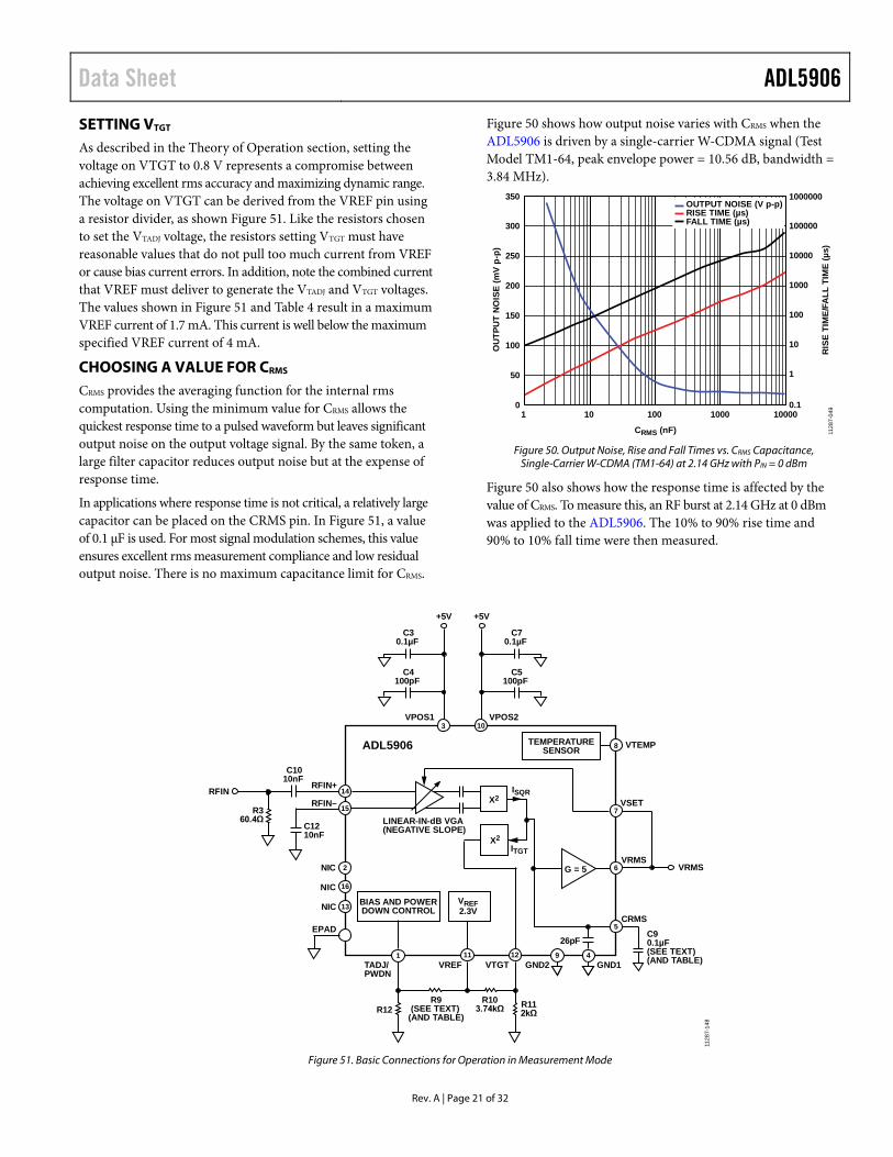
SETTING VTGT As described in the Theory of Operation section, setting the voltage on VTGT to 0.8 V represents a compromise between achieving excellent rms accuracy and maximizing dynamic range. The voltage on VTGT can be derived from the VREF pin using a resistor divider, as shown Figure 51. Like the resistors chosen to set the VTADJ voltage, the resistors setting VTGT must have reasonable values that do not pull too much current from VREF or cause bias current errors. In addition, note the combined current that VREF must deliver to generate the VTADJ and VTGT voltages. The values shown in Figure 51 and Table 4 result in a maximum VREF current of 1.7 mA. This current is well below the maximum specified VREF current of 4 mA.
CHOOSING A VALUE FOR CRMS
CRMS provides the averaging function for the internal rms computation. Using the minimum value for CRMS allows the quickest response time to a pulsed waveform but leaves significant output noise on the output voltage signal. By the same token, a large filter capacitor reduces output noise but at the expense of response time.
In applications where response time is not critical, a relatively large capacitor can be placed on the CRMS pin. In Figure 51, a value of 0.1 µF is used. For most signal modulation schemes, this value ensures excellent rms measurement compliance and low residual output noise. There is no maximum capacitance limit for CRMS.
Figure 50 shows how output noise varies with CRMS when the ADL5906 is driven by a single-carrier W-CDMA signal (Test Model TM1-64, peak envelope power = 10.56 dB, bandwidth = 3.84 MHz).
0.1
1
10
100
1000
10000
100000
1000000
0
50
100
150
200
250
300
350
1 10 100 1000 10000
RIS
E TI
ME/
FALL
TIM
E (µ
s)
OU
TPU
T N
OIS
E (m
V p-
p)
CRMS (nF)
OUTPUT NOISE (V p-p)RISE TIME (µs)FALL TIME (µs)
1128
7-04
9
Figure 50. Output Noise, Rise and Fall Times vs. CRMS Capacitance,
Single-Carrier W-CDMA (TM1-64) at 2.14 GHz with PIN = 0 dBm
Figure 50 also shows how the response time is affected by the value of CRMS. To measure this, an RF burst at 2.14 GHz at 0 dBm was applied to the ADL5906. The 10% to 90% rise time and 90% to 10% fall time were then measured.
C90.1µF(SEE TEXT)(AND TABLE)
R9(SEE TEXT)
(AND TABLE)
X2
BIAS AND POWERDOWN CONTROL
1
NIC
ITGT
LINEAR-IN-dB VGA(NEGATIVE SLOPE)
ISQR
26pF
2
VPOS1 VPOS23
GND1VREF VTGT GND2411
10
9
5CRMS
6VRMS
VRMS
7VSET
8
16
15
14
13
VTEMP
NIC
RFIN–
RFIN+
NIC
EPAD
ADL5906
12
X2
VREF2.3V
TEMPERATURESENSOR
G = 5
R360.4Ω
C1010nF
RFIN
C1210nF
R12 R112kΩ
R103.74kΩ
+5V
C30.1µF
C4100pF
C70.1µF
C5100pF
+5V
1128
7-14
8
TADJ/PWDN
Figure 51. Basic Connections for Operation in Measurement Mode

ADL5906 Data Sheet
Rev. A | Page 22 of 32
Table 5. Recommended Minimum CRMS Values for Various Modulation Schemes
Modulation/Standard Peak Envelope Power Ratio (dB)
Carrier Bandwidth (MHz) CRMSMIN (nF)
Output Noise (mV p-p)
Rise/Fall Time (µs)
QPSK, 5 MSPS (SQR COS Filter, α = 0.35) 3.8 5 1 84 0.2/10
QPSK ,15 MSPS (SQR COS Filter, α = 0.35) 3.8 15 1 42 0.2/10
64 QAM, 1 MSPS (SQR COS Filter, α = 0.35) 7.4 1 10 265 3/85
64 QAM, 5 MSPS (SQR COS Filter, α = 0.35) 7.4 5 1 380 0.2/10
64 QAM, 13 MSPS (SQR COS Filter, α = 0.35) 7.4 13 1 205 0.2/10
W-CDMA, One-Carrier, TM1-64 10.56 3.84 1 820 0.2/10 W-CDMA Four-Carrier, TM1-64, TM1-32, TM1-16, TM1-8 12.08 18.84 1 640 0.2/10 LTE, TM1, One-Carrier, 20 MHz (2048 QPSK Subcarriers) 11.58 20 1 140 0.2/10
Table 5 shows the recommended minimum values of CRMS for popular modulation schemes. Using lower capacitor values results in rms measurement errors. Output response time is also shown. If the output noise shown in Table 5 is unacceptably high, it can be reduced by
• Increasing CRMS • Implementing an averaging algorithm after the output voltage
of the ADL5906 has been sampled by an analog-to-digital converter (ADC)
The values in Table 5 were experimentally determined to be the minimum capacitance that ensures good rms accuracy for that particular signal type. This test was carried out by starting out with a large capacitance value on the CRMS pin (for example, 10 µF). The value of VRMS was noted for a fixed input power level (for example, −10 dBm). The value of CRMS was then progressively reduced (this can be done with press-down capacitors) until the value of VRMS started to deviate from its original value (this indicates that the accuracy of the rms computation is degrading and that CRMS is becoming too small).
In general, the minimum required rms averaging capacitance increases as the peak-to-average ratio of the carrier increases. The minimum required CRMS also tends to increase as the bandwidth of the carrier decreases. With narrow-band carriers, the noise spectrum of the VRMS output tends to have a correspondingly narrow profile. The relatively narrow spectral profile demands a larger value of CRMS that reduces the low-pass corner frequency of the averaging function and ensures a valid rms computation.
OUTPUT VOLTAGE SCALING The linear output voltage range of the ADL5906 is nominally 0.3 V to 3.7 V. VRMS is clamped to a maximum voltage of ~3.9 V; this helps improve falling edge settling speeds because the VRMS output stays closer to the nominal linear-in-dB output range of 0.3 V to 3.7 V. Within the 0 V to 3.9 V maximum output range, the slope can be adjusted as needed via extra resistors, as shown in Figure 52.
If only a part of the RF input power range of the ADL5906 is being used (for example, −10 dBm to −60 dBm), increase the scaling so that this reduced input range fits into the available output swing (0 V to 3.9 V) of the ADL5906.
The output swing is reduced by simply adding a voltage divider on the output pin, as shown in the A side of Figure 52. Reducing the output scaling can be used when interfacing the ADL5906 to an ADC with a 0 V to 2.5 V input range.
6
7VSET
R6
R2
VRMS6
7VSET
A B
R1
R15
VRMS
1128
7-14
9
Figure 52. Decreasing and Increasing Slope
The output voltage swing can be increased using a technique that is analogous to setting the gain of an op amp in noninverting mode (see the B side of Figure 52) with the VSET pin being the equivalent of the inverting input of the op amp.
With VRMS connected to VSET, the nominal transfer function of the ADL5906 is given by
VRMS = Slope × (PIN − Intercept)
For example at 3.5 GHz, with PIN equal to 0 dBm, the nominal output voltage is equal to 0.052 V/dB × (0 dBm − (−64 dBm) = 3.328 V.
To scale this voltage downward using a resistor divider, choose a value for R15 and calculate R1 using the following equation:
−×= 1'
RMS
RMS
VV
R15R1 (11)

Data Sheet ADL5906
Rev. A | Page 23 of 32
To scale this voltage upward, choose a value for R2 and calculate R6 using the following equation:
−= 1)||(
RMS
'RMS
IN VV
RR2R6 (12)
where: RIN is the input resistance of VSET (72 kΩ). V'RMS is the desired maximum output voltage. VRMS is the nominal maximum output voltage before scaling (see Figure 9 through Figure 26).
When choosing R1, R2, R6, and R15, notice the current drive capability of the VRMS pin and the input resistance of the VSET pin. The choice of resistors must not be too small because this results in excessive current drawn out of the VRMS pin (the VRMS pin can source a maximum current of 10 mA). However, choosing an R2 that is too large is also problematic. If the value of R2 chosen is compatible with the input resistance of the VSET pin (72 kΩ), this input resistance, which varies slightly from part to part, contributes to the resulting slope and output voltage. In general, ensure that the value of R2 is at least 10 times smaller than the input resistance of VSET. Therefore, the values for R6 and R2 must be in the 1 kΩ to 5 kΩ range. Similar values must be used for R1 and R15.
It is also important to take into account part-to-part and frequency variation in output swing along with the maximum output voltage (3.9 V) of the output stage of the ADL5906. The VRMS part-to-part distribution is well characterized at major frequency bands in the Typical Performance Characteristics section (see Figure 12 through Figure 14, Figure 18 through Figure 20, Figure 24, and Figure 25). The resistor values in Table 6, which were calculated based on 3.5 GHz operation, have been conservatively chosen so that there is no chance that the desired output voltage swings exceed the output swing of the ADL5906 (when scaling upward) or the input range of a 0 V to 2.5 V ADC (when scaling down-ward). In each case, the nominal maximum voltage that results is 100 mV below the desired maximum to account for part-to-part variation and resistor tolerances.
Table 6. Output Voltage Range Scaling Examples at 3.5 GHz
Desired Input Range (dBm) Slope Increase Slope Decrease
New Slope (mV/dB) Nominal Maximum Output Voltage (V) R6 (Ω) R2 (Ω) R1 (Ω) R15(Ω) 0 to −60 274 2000 59 3.8 −10 to −50 681 2000 70 3.8 0 to −60 787 2000 37 2.4 −10 to −50 348 2000 44 2.4

ADL5906 Data Sheet
Rev. A | Page 24 of 32
SYSTEM CALIBRATION AND ERROR CALCULATION The measured transfer function of the ADL5906 at 2.14 GHz is shown in Figure 53, which contains plots of both output voltage vs. input level and linearity error vs. input level. As the input level varies from −65 dBm to +5 dBm, the output voltage varies from ~0.25 V to ~3.9 V.
–6
–5
–4
–3
–2
–1
0
1
2
3
4
5
6
0
0.5
1.0
1.5
2.0
2.5
3.0
3.5
4.0
4.5
5.0
5.5
6.0
–65 –55 –45 –35 –25 –15 –5 5
ERR
OR
(dB
)
OU
TPU
T VO
LTA
GE
(V)
PIN (dBm) 1 128
7-05
1
OUTPUT VOLTAGE –40°COUTPUT VOLTAGE +25°COUTPUT VOLTAGE +85°CERROR –40°CERROR +25°CERROR +85°C
Figure 53. 2.14 GHz VRMS and Log Conformance Error at +25°C, −40°C, and
+85°C Using Two-Point Calibration at 0 dBm and −40 dBm
Because slope and intercept vary from device to device, board level calibration must be performed to achieve high accuracy. The equation for the idealized output voltage can be written as
VRMS(IDEAL) = Slope × (PIN − Intercept) (13)
where: Slope is the change in output voltage divided by the change in input power (dB). Intercept is the calculated input power level at which the output voltage is equal to 0 V (note that Intercept is an extrapolated theoretical value and not a measured value).
In general, calibration is performed during equipment manufacture by applying two or more known signal levels to the input of the ADL5906 and measuring the corresponding output voltages. The calibration points must be within the linear operating range of the device.
With a two-point calibration, the slope and intercept are calculated as follows:
Slope = (VRMS1 − VRMS2)/(PIN1 − PIN2) (14)
Intercept = PIN1 − (VRMS1/Slope) (15)
After the slope and intercept are calculated and stored in nonvolatile memory during equipment calibration, an equation can be used to calculate an unknown input power based on the output voltage of the detector.
PIN (Unknown) = (VRMS(MEASURED)/Slope) + Intercept (16)
The log conformance error is the difference between this straight line and the actual performance of the detector.
Error (dB) = (VRMS(MEASURED) − VRMS(IDEAL))/Slope (17)
Figure 53 includes a plot of this error at +25°C, −40°C, and +85°C when using a two-point calibration (calibration points are 0 dBm and −40 dBm). The error at the calibration points at 25°C (in this case, −40 dBm and 0 dBm) is equal to 0 dB by definition.
The residual nonlinearity of the transfer function that is apparent in the two-point calibration error plot can be reduced by increasing the number of calibration points. Figure 54 shows the post-calibration error plots for a three-point calibration. With a multipoint calibration, the transfer function is segmented, with each segment having its own slope and intercept. Multiple known power levels (three levels in this case) are applied, and multiple voltages are measured. When the equipment is in operation, the measured voltage from the detector is first used to determine which of the stored slope and intercept calibration coefficients are to be used. Then, the unknown power level is calculated by inserting the appropriate slope and intercept values into Equation 16.
When choosing calibration points, there is no requirement for, or value in, equal spacing between the points. There is also no limit to the number of calibration points used. However, when more calibration points are used, calibration time increases.
OU
TPU
T VO
LTA
GE
(V)
PIN (dBm)
–6
–5
–4
–3
–2
–1
0
1
2
3
4
5
6
0
0.5
1.0
1.5
2.0
2.5
3.0
3.5
4.0
4.5
5.0
5.5
6.0
–65 –55 –45 –35 –25 –15 –5 5ER
RO
R (d
B)
OUTPUT VOLTAGE –40°COUTPUT VOLTAGE +25°COUTPUT VOLTAGE +85°CERROR –40°CERROR +25°CERROR +85°C
1128
7-15
2
VTADJ = 0.35V
Figure 54. 2.14 GHz VRMS and Log Conformance Error at +25°C, −40°C, and
+85°C Using Three-Point Calibration at 0 dBm, −40 dBm, and −55 dBm
The −40°C and +85°C error plots in Figure 54 are generated using the +25°C slope and intercept values. This is consistent with equipment calibration in a mass production environment where calibration of multiple temperatures is not practical.

Data Sheet ADL5906
Rev. A | Page 25 of 32
USING VTEMP TO IMPROVE INTERCEPT TEMPERATURE DRIFT In applications where VTEMP and VRMS are both being digitized by an ADC, the VTEMP voltage can be used to further improve the temperature drift of the ADL5906.
As shown in Figure 54, whereas the slope is stable vs. the temperature at 2140 MHz, the intercept of the ADL5906 does vary slightly vs. temperature (approximately +0.3 dB at +85°C and −0.8 dB at −40°C). This variation in intercept is constant vs. input power level at most frequencies. Table 7 lists the average temperature coefficient of VRMS in mV/°C at frequencies from 100 MHz to 5.8 GHz. This temperature coefficient is given by the following equation:
TCVRMS = (DRIFTVRMS/ΔTEMP) × Slope (18)
where: DRIFTVRMS is the specified drift of VRMS (scaled in dB) from ambient to either −40°C or +85°C at an input power level of 0 dBm (see Table 1). ∆TEMP is equal to either +65°C for cold drift (that is, +25°C − (−40°C)) or +60°C for hot drift (that is, +85°C − +25°C). Slope is the specified slope of VRMS (see Table 1).
For example, at 2.14 GHz, TCVRMS for hot drift can be calculated as
TCVRMS = (0.3 dB/60°C) × 56 mV/dB = 0.28 mV/°C
The value for slope that is used can also be the slope that is calculated during device calibration. This gives results that are slightly more accurate because there is slight variation in slope from device to device.
Table 7 also lists the typical temperature coefficient of the VTEMP temperature sensor output. To calculate the appropriate amount of compensation required at a particular frequency, a VTEMP weighting factor is calculated. This is simply the ratio of the temperature coefficients of VTEMP and VRMS. These weighting factors are also shown in Table 7.
Using the data shown in Table 7, an adjusted value for VRMS (VRMS‘) can be calculated using the following equation:
−−=
FactorWeightingVV
V'V TEMP25TEMPRMSRMS (19)
where: VTEMP25 is equal to the voltage measured on VTEMP during system calibration at ambient temperature. VTEMP is equal to the voltage on VTEMP during normal operation.
Figure 55 to Figure 62 show typical plots of VRMS’ vs. input level and temperature at frequencies from 100 MHz to 5.8 GHz when this temperature compensation algorithm is applied.
From a system calibration and operation perspective, the only additional measurements that are required to implement this algorithm are measurement and storage of VTEMP during calibration (that is, at ambient temperature) and measurement of VTEMP during operation. All other information required to implement this algorithm (that is, nominal temperature drift of VRMS and temperature coefficient of VTEMP) is based on typical data sheet specifications.
–6
–5
–4
–3
–2
–1
0
1
2
3
4
5
6
0
0.5
1.0
1.5
2.0
2.5
3.0
3.5
4.0
4.5
5.0
5.5
6.0
–65 –55 –45 –35 –25 –15 –5 5
ERR
OR
(dB
)
V RM
S' (V
)
PIN (dBm)
VRMS' –40°CVRMS' +25°CVRMS' +85°CERROR –40°CERROR +25°CERROR +85°C
1128
7-15
3
VTADJ = 0.35V
Figure 55. VRMS’ and Log Conformance Error vs. Input Level and Temperature
at 100 MHz Using VTEMP Intercept Compensation
–65 –55 –45 –35 –25 –15 –5 5
PIN (dBm)
–6
–5
–4
–3
–2
–1
0
1
2
3
4
5
6
0
0.5
1.0
1.5
2.0
2.5
3.0
3.5
4.0
4.5
5.0
5.5
6.0
ERR
OR
(dB
)
V RM
S' (V
)
VRMS' –40°CVRMS' +25°CVRMS' +85°CERROR –40°CERROR +25°CERROR +85°C
1 128
7-05
4
VTADJ = 0.35V
Figure 56. VRMS’ and Log Conformance Error vs. Input Level and Temperature
at 700 MHz Using VTEMP Intercept Compensation

ADL5906 Data Sheet
Rev. A | Page 26 of 32
–65 –55 –45 –35 –25 –15 –5 5
PIN (dBm)
–6
–5
–4
–3
–2
–1
0
1
2
3
4
5
6
0
0.5
1.0
1.5
2.0
2.5
3.0
3.5
4.0
4.5
5.0
5.5
6.0
ERR
OR
(dB
)
V RM
S'(V
)
1128
7-15
5
VRMS' –40°CVRMS' +25°CVRMS' +85°CERROR –40°CERROR +25°CERROR +85°C
VTADJ = 0.35V
Figure 57. VRMS’ and Log Conformance Error vs. Input Level and Temperature
at 900 MHz Using VTEMP Intercept Compensation
PIN (dBm)
–6
–5
–4
–3
–2
–1
0
1
2
3
4
5
6
0
0.5
1.0
1.5
2.0
2.5
3.0
3.5
4.0
4.5
5.0
5.5
6.0
–65 –55 –45 –35 –25 –15 –5 5
ERR
OR
(dB
)
V RM
S' (V
)
VRMS' –40°CVRMS' +25°CVRMS' +85°CERROR –40°CERROR +25°CERROR +85°C
1128
7-15
6
VTADJ = 0.35V
Figure 58. VRMS’ and Log Conformance Error vs. Input Level and Temperature
at 1900 MHz Using VTEMP Intercept Compensation
PIN (dBm)
–6
–5
–4
–3
–2
–1
0
1
2
3
4
5
6
0
0.5
1.0
1.5
2.0
2.5
3.0
3.5
4.0
4.5
5.0
5.5
6.0
–65 –55 –45 –35 –25 –15 –5 5
ERR
OR
(dB
)
V RM
S' (V
)
1128
7-05
7
VRMS' –40°CVRMS' +25°CVRMS' +85°CERROR –40°CERROR +25°CERROR +85°C
VTADJ = 0.35V
Figure 59. VRMS’ and Log Conformance Error vs. Input Level and Temperature
at 2140 MHz using VTEMP Intercept Compensation
PIN (dBm)
–6
–5
–4
–3
–2
–1
0
1
2
3
4
5
6
0
0.5
1.0
1.5
2.0
2.5
3.0
3.5
4.0
4.5
5.0
5.5
6.0
–65 –55 –45 –35 –25 –15 –5 5
ERR
OR
(dB
)
V RM
S' (V
)
VRMS' –40°CVRMS' +25°CVRMS' +85°CERROR –40°CERROR +25°CERROR +85°C
1128
7-05
8
VTADJ = 0.4V
Figure 60. VRMS’ and Log Conformance Error vs. Input Level and Temperature at 2600 MHz Using VTEMP Intercept Compensation
–6
–5
–4
–3
–2
–1
0
1
2
3
4
5
6
0
0.5
1.0
1.5
2.0
2.5
3.0
3.5
4.0
4.5
5.0
5.5
6.0
–65 –55 –45 –35 –25 –15 –5 5
ERR
OR
(dB
)
V RM
S' (V
)
PIN (dBm)
1128
7-05
9
VRMS' –40°CVRMS' +25°CVRMS' +85°CERROR –40°CERROR +25°CERROR +85°C
VTADJ = 0.45V
Figure 61. VRMS’ and Log Conformance Error vs. Input Level and Temperature
at 3500 MHz Using VTEMP Intercept Compensation
–6
–5
–4
–3
–2
–1
0
1
2
3
4
5
6
0
0.5
1.0
1.5
2.0
2.5
3.0
3.5
4.0
4.5
5.0
5.5
6.0
–65 –55 –45 –35 –25 –15 –5 5
ERR
OR
(dB
)
V RM
S' (V
)
PIN (dBm)
1128
7-06
0
VRMS' –40°CVRMS' +25°CVRMS' +85°CERROR –40°CERROR +25°CERROR +85°C
VTADJ = 1V
Figure 62. VRMS’ and Log Conformance Error vs. Input Level and Temperature
at 5800 MHz Using VTEMP Intercept Compensation

Data Sheet ADL5906
Rev. A | Page 27 of 32
Table 7. Scaling Factors for Intercept Temperature Drift Compensation Using VTEMP
Frequency (MHz)
TCVRMS, −40°C to +25°C, PIN = 0 dBm (mV/°C)
TCVRMS, 25°C to 85°C, PIN = 0 dBm (mV/°C)
TCVTEMP
(mV/°C)
VTEMP Weighting Factor, −40°C to +25°C (TCVTEMP/TCVRMS)
VTEMP Weighting Factor, +25°C to +85°C (TCVTEMP/TCVRMS)
100 0.72615 0.19667 4.8 6.61017 24.40678 700 0.81692 0.295 4.8 5.87571 16.27119 900 0.72615 0.295 4.8 6.61017 16.27119 1900 0.70154 0.19 4.8 6.84211 25.26316 2140 0.68923 0.28 4.8 6.96429 17.14286 2600 0.76154 0.275 4.8 6.30303 17.45455 3500 1.2 0 4.8 4 ∞ 5800 1.23931 0.08041 4.8 5.99417 85.287
1TCVRMS based on temperature drift at PIN = −10 dBm.
DESCRIPTION OF CHARACTERIZATION For a description on how characterization was completed, see the ADL5902 data sheet.

ADL5906 Data Sheet
Rev. A | Page 28 of 32
EVALUATION BOARD The ADL5906-EVALZ is a fully populated, 4-layer, FR4-based evaluation board. For normal operation, it requires a 5 V/100 mA power supply. The 5 V power supply must be connected to the VPOS and GND test loops. The RF input
signal is applied to the SMA connector (RFIN). The output voltage is available on the SMA connector (VOUT1) or on the test loop (VOUT). Configuration options for the evaluation board are listed in Table 8.
X2
BIAS AND POWERDOWN CONTROL
1
NIC
ITGT
LINEAR-IN-dB VGA(NEGATIVE SLOPE)
IDET
26pF
2
VPOS1 VPOS23
GND1VREF VTGT GND2411
10
9
5CRMS
C90.1µF
6VRMS
7VSET
8
16
15
14
13
VTEMP
NIC
RFIN–
RFIN+
NIC
EPAD
ADL5906
12
X2
VREF2.3V
TEMPERATURESENSOR
G = 5
R360.4Ω
C1010nF
RFIN
TC2
VOUT
VOUT1
VREF VTGT
GND
C1210nF
R12270Ω
R91.5kΩ
R112kΩ
R103.74kΩ
R60Ω
R10Ω
R2(OPEN)
R15(OPEN)
VSET
VPOS
C30.1µF
C4100pF
C70.1µF
C5100pF
1128
7-15
0
TADJ/PWDN
Figure 63. Evaluation Board Schematic
Table 8. Evaluation Board Configuration Options Component Function/Notes Default Value RFIN, R3, C10, C12
RF input. The evaluation board is configured for single-ended drive on the RFIN+ pin (Pin 14). Capacitors C10 and C12 have been set large enough so that the full frequency range of the device is covered. If operation down to 10 MHz is not required, the value of these capacitors can be reduced.
RFIN = SMA connector, C10 = C12 = 10 nF, R3 = 60.4 Ω
VTGT, R10, R11
VTGT interface. R10 and R11 are set up to provide 0.8 V to VTGT derived from VREF. If R10 and R11 are removed, an external voltage can be applied on the VTGT test point.
VTGT = black test loop, R10 = 3.74 kΩ, R11 = 2 kΩ, VTGT = 0.8 V
VPOS, GND, C3, C4, C5,C7
Power supply interface and decoupling. Apply the power supply for the evaluation board to the VPOS and GND test loops. The nominal supply decoupling consists of a 100 pF capacitor and a 0.1 μF capacitor on each power supply pin, with the 100 pF capacitor placed closer to the pin.
VPOS = red test loop, GND = black test loop, C3 = C7 = 0.1 μF, C4 = C5 = 100 pF

Data Sheet ADL5906
Rev. A | Page 29 of 32
Component Function/Notes Default Value VOUT, VOUT1, VSET, R1, R2, R6, R15
Output interface. In measurement mode, a portion of the voltage at the VRMS pin is fed back to the VSET pin via R6 (R6 is normally set to 0 Ω). Using the voltage divider created by R2 and R6, the magnitude of the slope of VRMS is increased by reducing the portion of VRMS that is fed back to VSET. Resistors R1 and R15 can be used to reduce the output slope.
VOUT = black test loop, VOUT1 = SMA connector, VSET = black test loop, R1 = R6 = 0 Ω, R15 = R2 = open
In controller mode, R6 must be open. In this mode, the ADL5906 can control the gain of a variable gain amplifier (VGA) or voltage variable attenuator (VVA). A setpoint voltage is applied to the VSET test loop, and the VRMS test loop or SMA connector drives the gain control input of the VGA/VVA.
C9 RMS averaging capacitor. The value of the rms averaging capacitor should be set based on the peak-to-average ratio of the input signal and based on the desired output response time and residual output noise.
C9 = 0.1 µF
TC2, R9, R12 TADJ/PWDN interface. The TADJ/PWDN pin controls the slope temperature compensation and/or shuts down the device. The evaluation board is configured with VTADJ connected to VREF through a resistor divider (R9, R12). This voltage divider can be removed (or simply overdriven) allowing for the external application of a voltage to the VTADJ pin by applying a voltage to the TC2 test point.
TC2 = black test loop, R9 = 1.5 kΩ, R12 = 270 Ω, VTADJ = 0.35 V
EVALUATION BOARD ASSEMBLY DRAWINGS 11
287-
055
Figure 64. ADL5906 Evaluation Board Layout, Top Side
1128
7-05
6
Figure 65. ADL5906 Evaluation Board Layout, Bottom Side
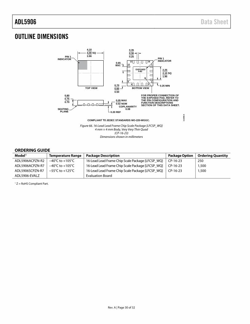
ADL5906 Data Sheet
Rev. A | Page 30 of 32
OUTLINE DIMENSIONS
COMPLIANT TO JEDEC STANDARDS MO-220-WGGC. 1119
08-A
10.65BSC
BOTTOM VIEWTOP VIEW
16
589
1213
4
EXPOSEDPAD
PIN 1INDICATOR
4.104.00 SQ3.90
0.700.600.50
SEATINGPLANE
0.800.750.70 0.05 MAX
0.02 NOM
0.20 REF
0.25 MIN
COPLANARITY0.08
PIN 1INDICATOR
0.350.300.25
2.252.10 SQ1.95
FOR PROPER CONNECTION OFTHE EXPOSED PAD, REFER TOTHE PIN CONFIGURATION ANDFUNCTION DESCRIPTIONSSECTION OF THIS DATA SHEET.
Figure 66. 16-Lead Lead Frame Chip Scale Package [LFCSP_WQ]
4 mm × 4 mm Body, Very Very Thin Quad (CP-16-23)
Dimensions shown in millimeters
ORDERING GUIDE Model1 Temperature Range Package Description Package Option Ordering Quantity ADL5906ACPZN-R2 −40°C to +105°C 16-Lead Lead Frame Chip Scale Package [LFCSP_WQ] CP-16-23 250 ADL5906ACPZN-R7 −40°C to +105°C 16-Lead Lead Frame Chip Scale Package [LFCSP_WQ] CP-16-23 1,500 ADL5906SCPZN-R7 −55°C to +125°C 16-Lead Lead Frame Chip Scale Package [LFCSP_WQ] CP-16-23 1,500 ADL5906-EVALZ Evaluation Board 1 Z = RoHS Compliant Part.

Data Sheet ADL5906
Rev. A | Page 31 of 32
NOTES

ADL5906 Data Sheet
Rev. A | Page 32 of 32
NOTES
©2013 Analog Devices, Inc. All rights reserved. Trademarks and registered trademarks are the property of their respective owners. D11287-0-10/13(A)