Embed Size (px)
Citation preview
290 SCIENCE AND CULTURE, NOVEMBER-DECEMBER, 2015
SOLIDSTATE LIGHTING
D.V. SRIDHARA RAO1, K. MURALEEDHARAN2 AND R. MURALIDHARAN3
Lighting is an integral part of human life. Globally, about 15% of the generated power is spentfor the lighting applications. In this context, the recent advances in 'solid state lighting (SSL)' arevery important to promote energy savings and reduce green house gas emissions. This articlepresents an overview of advancements in SSL with focus on GaN light emitting diode (LED), itsimpact on energy savings and relevance to India.
ARTICLE
1 Defence Metallurgical Research Laboratory, DRDO, Hyderabad,e-mail : [email protected]
2 CSIR-CGCRI, Kolkata, e-mail : [email protected] CENSE, Indian Institute of Science, Bengaluru, e-mail :
Introduction
From time immemorial, lighting has become anintegral part of all life forms and central to theexistence of life. Light has revolutionised our living
and has positive impact on energy, communications,education, health, vision, life sciences and entertainment.Hence, in order to highlight the importance of lighting,the UN General Assembly declared the year 2015 asInternational year of light and light-based technologies.It can be stated that lighting is directly linked to theadvancement of human civilisation. The early man did mostof the activities under day light and used fire, by burningdry leaves and fire wood, for night lighting and protectionagainst wild animals. With the progress of civilisation, waxcandles and oil lamps were used and the real breakthroughin lighting took place in 1879 in the form of incandescentlight (ICL) source developed by Thomas Alva Edison. Ithas a tungsten filament enclosed in an evacuated glass bulband the passage of electric current resulted in Joule’sheating of the filament and the resultant glow is used forlighting. Thus, ICL source is like the fire in a glass bulbwith only about 5% of input energy manifesting as lightand the rest wasting as heat. It is to be noted that ‘Watt(W)’ is the measure of electricity, ‘Lumen (lm)’ is theluminous flux or measure of total amount of light emitted
by the source in a solid angle of one steradian and emittedtowards all directions with a luminous intensity of onecandle, and ‘luminous efficacy (lm/W)’ represents the totalluminous flux emitted by light source divided by itswattage. The typical luminous efficacy of the tungstenfilament bulb is very low (about 10-15 lm/W) with a typicallife span of about 1000-1500 hours under regular householdusage conditions. The fluorescent lamp (FL) technologywas developed in late 1930’s and it has an improvedluminous efficacy (40-70 lm/W) and offered about 70-80%energy savings over the ICL source. These lamps are inthe form of linear fluorescent (tubular) and compactfluorescent lamps (CFLs) and can last longer (about 5-10times compared to ICLs). Later, the halogen lamp (50-70lm/W) and high-pressure sodium vapour lamp (80-150 lm/W) technologies were developed however mostly used foroutdoor lighting. The path-breaking revolution in lightingstarted quite recently with the advent of solid state lighting(SSL) in the form of Gallium Nitride (GaN) based brightblue light emitting diodes (LEDs1,2,3). The LED has muchhigher luminous efficacy (Cree Inc., demonstrated a valueof 300 lm/W in 2014 for blue LED source) and nowadays,the manufacturers routinely produce LED bulbs with anefficacy of the order of 100-150 lm/W. Therefore,replacing LED bulbs in place of fluorescent lights (CFLs,tube lights and fluorescent bulbs) can potentially save 50%of power consumption. Also, the LEDs have long life(about 8-10 times compared to CFLs and 50 times morethan ordinary filament bulbs), thus minimal replacementsduring one’s whole life. Hence, LED bulb was rightly
VOL. 81, NOS. 11–12 291
described by our honourable prime minister, Sri NarendraModi, as a ‘Prakash Path’ (way to light). The differentlight sources are shown in Fig. 1. It is to be noted thatthe organic LEDs (OLEDs) are also based onsemiconductors and consists of thin layers of organic
95% of them are in rural areas. They depend on non-commercial sources of energy such as biomass, agricultureresidue, fuel wood and kerosene for cooking and lighting.In this regard, the nation spends approximately US$2 billionper annum for the kerosene subsidy bill (total subsidy for
Fig. 1. Photograph of some light sources : (a) incandescent lamp, (b) mercury vapour lamp, (c) high pressure sodium vapour lamp, (d) metal halidelamp, (e) linear fluorescent lamp (tube light), (f) compact fluorescent lamp (CFL), (g) LED
molecules, which generate light with drive current.Currently, the efficiency of OLEDs is very low vis-a-visGaN LEDs. It holds the future as it offers flexibility,besides less power consumption. Semiconductors lasersand single photon sources are also light sources and theyhave very specialised applications; they are in general notused for the traditional lighting applications. Hence, thesetopics are outside the scope of this article.
Lighting: Global and Indian Scenario4,5,6
Lighting is needed for indoor and outdoorapplications, viz., lighting for household and commercialbuildings, street lighting, high-way lighting, traffic lighting,lighting in the public places etc. Globally, about 15% ofthe generated power is spent for the lighting applicationsand a similar statistics (about 18%) holds good for India.It is alarming to note that about one-third of the globalpopulation is off-power grids and still lives on primitivesources (viz., fire wood and kerosene lamps etc, which haveultralow luminous efficacy, < 1 lm/W) for lighting andspends about US$30 billion per annum on fuel for lighting.Especially, vast portions of the rural India suffer from eitherunder-electrification or off-grid. It is estimated that about1/3rd of the households in India are off-the grid and about
kerosene is about US$4 billion and 50% of it goes towardslighting). This is disheartening inequity for the 21st centuryand needs to be quickly addressed by the policy makers.Also, the firewood burning releases suffocating emissionsand particulates thereby causing indoor pollution. Sincemany developing countries and underdeveloped countriesgenerate the electric power through the conventionalmethods, viz., thermal power plants in which coal is burntto generate electricity, the resultant emissions leave carbonfoot print and cause global warming, besides air and landpollution. Therefore, since lighting constitutes a lion shareof the power generation, the lighting technology with betterenergy efficiency is the need of the hour for the sustainabledevelopment. Hence, due to its very low luminous efficacy,the incandescent lamp (ICL) was banned in manydeveloped countries and several countries are doing it in aphased manner, i.e., ICL is in the verge of global switch-off ! India is also following this trend, viz., themanufacturing of ICLs of 150W or higher and high wattagehalogen lamps have been stopped. The alternate to ICL isCFL, whose initial cost is comparatively high, however canbe compensated due to its more longevity and energysavings. For example, 13-15 W CFL can replace 60 WICL India has about 400 million household lamps (mostly

292 SCIENCE AND CULTURE, NOVEMBER-DECEMBER, 2015
incandescent bulbs) consuming over 70 TWh annually andthe replacement with CFLs can promote energy saving by80% and substantially reduce the CO2 emissions. Similarly,public lighting requires about 5000 MW and this can besubstantially reduced by adopting CFL lighting. Hence, inorder to promote energy efficiency, Government of Indialaunched ‘Bachat Lamp Yojana program, 2009’, aimed atbulk procurement and distribution of CFLs at subsidisedprices (CFL in exchange of ICL and payment of Rs. 15).This program was developed by Bureau of EnergyEfficiency under the aegis of Ministry of Power and wasregistered under the Clean Development Mechanism(CDM) of the Kyoto Protocal. Due to the governmentand private initiatives, the CFL sales jumped from 20million units in 2004 to 500 million units in 2014.However, despite the energy saving merit, the CFLtechnology has its demerits & limitations, viz., many peopletreat CFL light as dim and unpleasant. Also, the CFLscontain mercury (about 5 mg of amalgamated mercury perbulb), which is toxic and has environmental and healthhazards. Hence, the global focus shifted to solid statelighting technology, which involves light-emitting diode(LED), as it provides cleaner technology (reduce the levelof CO2 emission, hence contribute positively to the climatechange) with better energy savings (For example, 5-6WLED bulb can replace 40W ICL and 16W tube LED canreplace 40W tube fluorescent lamp) and minimalreplacements in one’s own life time. Therefore, in India,during the phase-2 (2012-17) of Bachat Lamp Yojanaprogram, it is planned to provide LED bulbs in place ofCFLs. For example, Karnataka state alone is planning tooffer 60 million LED bulbs to the households andreplacement of 1.2 million street lights in 220 urban localbodies, at a project cost of Rs.2600 crore, to beimplemented through Energy Efficiency Services Ltd(EESL), a Government of India enterprise. This step islikely to save about 800-1000 MW power. Other statesare also planning for the LED bulb usage.
Evolution of Solid State Lighting
Lighting: Some Basics : The human eye has sensorycells for vision and sensing light. The human vision isinsensitive to the radiation in the infrared and ultravioletparts of the electromagnetic spectrum and has spectralsensitivity in visible range. Our retina consists of 6 millioncones and 120 million rods. The cones are responsible forcolor vision while the rods are color-blind. The conesfunction best in bright light, while the rods are responsiblefor night vision. They exhibit spectral response with peakvalues at 555 nm and 507 nm respectively. The humaneye uses scotopic vision (low-light condition), mesopic
vision (intermediate condition) and photopic vision (well-lit condition). The photopic vision gives colour perceptionand higher temporal resolution and visual acuity thanavailable with scotopic vision. Hence, it is important toknow the S/P ratio, spectral power distribution (SPD) andeffective luminance factor (ratio of mesopic luminance tophotopic luminance) besides the luminous efficacy of thelight source.
The light source is defined by different characteristicssuch as luminous efficacy, luminaire efficacy, colouraccuracy (colour rendering index, CRI), light colour orcolour quality (correlated colour temperature, CCT), lightoutput & distribution and lumen depreciation. The LEDbulbs (or luminaire) consist of LED source and powersupply/drivers for providing the required input currents.The luminous efficacy is the LED source efficacy,expressed as the ratio luminous flux emitted by the sourceto light source wattage, without including the power supply/driver. It is a measure of the efficiency of the source toproduce visible light from electricity. Luminaire efficacyis calculated by taking into account of the wattage of thepower supply/driver. CRI is a measure of how naturalcolors will appear when an object is illuminated by a lightsource (CRI-100 is excellent and all colours are clearlyrepeatable, CRI-80 implies some colours look alike andCRI-70 is poor and most colours can’t be distinguished).Generally a CRI of 70 and above will be required for mostlighting applications. The colour quality is indicated inCCT, which is measure of the “shade” of whiteness of alight source compared with a blackbody radiator, measuredin K. The energy star specifications for LEDs range from2700K (typical CCT for incandescent lamps) to 6500K(typical CCT for day light). In general, the warm white’sCCT is below 3000K (red to yellow), bright white in therange of 3000-4500K and cool white (white light that ismissing the red wavelengths) is 5000 K and above. Thecool white (also called lunar white) appears bluish to theeye. The light output & distribution is related to the beamangle and shows whether the light is diffused or directed.For example, the light radiated by an ICL source has abeam angle of about 270°, hence it is diffused; the LEDlighting has relatively low beam angles, hence it is directed.For traditional light sources, lamp failure is the basis forlife time (40% of life time is considered for fluorescentlamps and metal halide lamps), however for LED, thelumen depreciation is considered as it gradually diminishesits output. In this context, L50 and L70 (estimated operatinghours to 50% and 70% of initial light output).
The performance of LEDs is indicated by differenttypes of efficiencies, viz., injection efficiency (IE), internal

VOL. 81, NOS. 11–12 293
quantum efficiency (IQE), extraction efficiency (EE) oroptical efficiency (OE), external quantum efficiency (EQE)and wall plug efficiency (WE) or radiant efficiency. InLED, the electron-hole recombination generates photons.This takes place by injecting the electrons into the activeregion, which is indicated by IE. It is to be noted that theelectron-hole recombinations are either non-radiative orradiative; IQE is the proportion of the radiativerecombinations (producing photons) to the totalrecombinations. All photons produced in the active regionare not emitted by the LED. EE represents the proportionof these generated photons emitted by the LED device.EQE is how efficiently the LED converts electrons intophotons and emits. WE is the efficiency of convertingelectrical to optical power.
Semiconductor Quantum Wells (QW) forLighting : The present bright white LED technology isbased on III-V compound semiconductors (primarily GaN,InN and AlN base alloys) grown in the form of epitaxialmultilayered thin films. They work in the domain of thelaws of quantum physics. In general, physics can beclassified into two broad categories: classical physics orNewtonian Physics (describes macroscopic objects/phenomenon in which electron properties are described byconsidering it as a particle) and quantum physics(microscopic objects in which electron exhibits wavenature). The quantum physics was developed by Max
Planck, Heisenberg, Einstein, Schrodinger etc. In simplewords, the laws of quantum mechanics operate if thematerial size is reduced to the scale of few nanometersalong at least one of the three dimensions (i.e., tiny world).This is the basis for the concepts of quantum well, quantumwire and quantum dot. In the respective cases, the materialis in nanometer scale along one, two and three dimensionsrespectively. In the quantum world, the material exhibitsdiscrete energy levels (in place of energy bands in a typicalbulk material), which are dependent on composition, strainand material’s size such as thickness. Due to this quantizedphenomenon, the electrons exhibit certain extraordinaryproperties (high electron mobility, very small thresholdcurrents, better carrier injection, improved radiativerecombination etc), hence used in semiconductor lasers,LEDs and high-electron mobility transistors.
The typical blue LED device is made up of thin(typical thickness ~2-4 nm) epitaxial single crystallinelayers of InxGa1-xN quantum wells (QWs) embeddedbetween GaN barrier layers (typical thickness ~10-20 nm)(refer Fig.2). They are grown by thin film depositionmethods (viz., molecular beam epitaxy, organometallicvapour phase epitaxy) on suitable single crystallinesubstrates, such as GaN, sapphire, silicon and SiC. InGaNhas a relatively lower energy band gap vis-a-vis GaN. Also,this wurtzite materials system exhibits polarity along thec-axis. The heterojunction across the InGaN-GaN layersresult in energy band offsets, whereas the internalpolarisation electric fields direct the free carriers (electronsand holes) to flow to the InGaN region. The size effect(finite thickness of InGaN layer) result in the formation ofdiscrete energy states (in place of continuous energy band)and the carriers exhibit quantum confinement effects, viz.,electrons exhibit wave nature and flow like a highly mobiletwo-dimensional sheet parallel to the interfaces with ballisticconduction properties, hence this layer is called as quantumwell (QW). The GaN layers act as potential barriers andthe band offsets enhances the carrier confinement to theInGaN layer very effectively. By placing such a thinInGaN layer between p-GaN (Mg-doped GaN) and n-GaN(Si-doped GaN) layers and application of small voltage(called forward biasing) of this structure through suitableohmic contacts (for example, palladium) results in theinjection of the majority carriers (electrons in n-GaN andholes in p-GaN) to the QW region for recombination andthese radiative recombination causes the emission ofphotons with wavelength corresponding to the intrinsicbandgap of the InGaN layer (viz., In0.2Ga0.8N emits bluelight). This is how blue light is produced by GaN LED.In commercial scale, the dominant approach for obtainingwhite light is that this generated blue light is passed through
Fig. 2. Cross-sectional TEM image of LED device structure showingInGaN quantum wells embedded between GaN barrier layers. The lightemission takes place from these quantum wells.
294 SCIENCE AND CULTURE, NOVEMBER-DECEMBER, 2015
a yellow-phosphor coating. The resultant light is bluishwhite in colour.
Historically, the size quantisation effects insemiconductor quantum wells were extensively studied bythe IBM team in 1970’s (Esaki, Tsu and Chang), whichsubsequently led to the development of several electronicand optoelectronic devices (for example, QW laser in 1979and high-electron mobility transistor in 1980). It is to benoted that the theory of quantum size effects originatedwell before the experimental demonstration, primarily dueto the slow pace of advancements in instrumentation.
LEDs: Some early efforts & Development of GaNtechnology : The early efforts on solid state lighting wereby Henry Joseph Round (1907) and Oleg VladimirovichLossev (1920), however, the efficiency of light generationwas abysmally low (0.05%). The real breakthrough camewith GaAs and GaP system, and in the form of GaAs basedinfrared LED. Then, red and green LEDs (based on thealloys of GaP and GaAs) and green LEDs based on N-doped GaP technology. All these developments took placeduring 1950-70, due to the efforts of Welker, Holonyak,Pankoev et al.
For solid state lighting, white light is needed, whichcan be realised through mixing blue (B), green (G) andred (R) lights. Green and red LEDs can be made fromGaAs and GaP alloys. AlGaAs is suitable for infrared andred lighting but not for short wavelengths. However, allthese material systems are unsuitable for the bluewavelengths. Hence, the earlier efforts for bluewavelengths were focussed on zinc selenide materialsystem, but the efficiency was poor. Later, GaN systemwas identified at RCA (Radio Corporation of America,USA) in 1968 by Herbert Paul Maruska and Tietzen. Infact, this activity at RCA was not for SSL applications butfor making LED TVs! In the subsequent year, the first
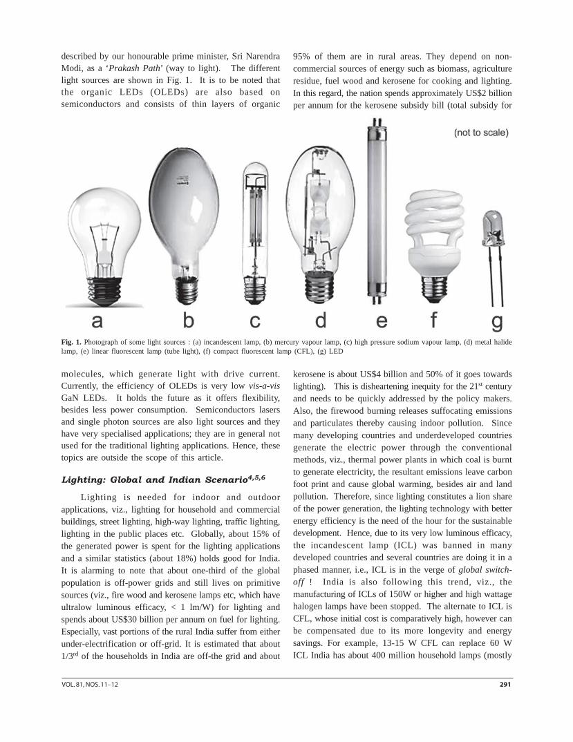
paper on the growth of GaN crystals (by halide vapourphase epitaxy (HVPE)) on sapphire was published. Afterfew years, Ed Miller and Jacques Pankove joined RCAand made a green LED (in 1971) using zinc-doped GaN/n-GaN/transparent layer of indium (bottom layer). In thesubsequent year, the bright violet LED emitting at 430 nmwas demonstrated by Maruska, by replacing zinc dopantswith magnesium dopants. RCA was collapsing in 1974 andthe GaN activity came to a standstill at this place. Theefficiency of this LED was poor, which was due to poorcrystalline quality of GaN, viz., the GaN films wereheteroepitaxially grown on sapphire (due to lack of GaNsubstrates at that time) and the associated large latticemismatch (about 16%) and thermal mismatch (about 34%)generate high density of microstructural defects (pointdefects, line defects and volume defects and importantlythreading dislocations ~ 1010 cm-2). A representative cross-sectional TEM image showing the threading dislocationsin GaN film is shown in Fig. 3. Also, the direct growth ofGaN on sapphire formed randomly oriented GaN nuclei,which is undesirable for single crystallinity. Despite thesedrawbacks, the Japanese teams (Hiroshi Amano and IsamuAkasaki, Nagoyo University) and Shuji Nakamura (NichiaChemical Industries Corporation, now in UCSB) pursuedresearch and developed methodologies to grow goodcrystalline quality GaN films2,3. In 1985, Amano andAkasaki demonstrated a two-step growth method involvingthe growth of low temperature AlN nucleation layer (NL)followed by high temperature GaN layer growth. At thattime, p-type doping of GaN was difficult and themagnesium dopant forms a deep acceptor state, hence theactivation of this dopant was very less efficient. Due totheir research efforts, in 1989, p-type GaN with goodconductivity was achieved by low-energy electron beamirradiation. Shuji Nakamura, during 1989-93, developed anew two-step growth approach for realising good crystallinequality GaN films, viz., low-temperature GaN NL followedby high-temperature GaN layer growth. Also, the activationof Mg dopants was achieved by thermal annealing process.Thus, the twin issues of growth of good quality GaN filmsand p-type GaN were addressed by them independently.Nakamura also credited with the development of InGaN/GaN double-heterostructure blue LED and laser. It tookalmost 30 years for the development of high brightnessblue LEDs. Due to these efforts, the Japanese trio,Nakamura, Akasaki and Amano were awarded the NobelPrize for physics for the year 2015.
Key issues: Further developments of solid statelighting technology depend upon the following issues :(i) Substrates: The choice of a suitable substrate decides
Fig. 3. Cross-sectional TEM image (imaged under weak-beam dark fieldconditions) showing the threading dislocations (thin bright contrast linesrunning parallel to the growth directions) in GaN film epitaxially grownon sapphire substrate with AlN buffer.

VOL. 81, NOS. 11–12 295
the quality of LED device structures. The commercialprogress of Si, GaAs and InP technologies was largely dueto the availability of native single crystals and substrates.In the respective cases, the lattice mismatch and thermalmismatch favour the growth of device structures & epitaxialfilms with minimal structural defects. However, untilrecently, GaN bulk single crystal could be grown only invery small sizes (few mm in size, by process called highpressure solution growth) and the technology for makinglarge-sized single crystal bulk GaN crystal (by processcalled ammonothermal growth) came up of late, but itscommercial availability and extraordinary cost are majorlimitations. GaN bulk-like growth (by Halide vapour phaseepitaxy) was also explored, in which thick GaN epilayerwas grown on sapphire, subsequently debonded and thefree-standing GaN can be used as a substrate. However,due to these various manufacturing issues and cost factors,the commercial GaN LEDs are widely grown on siliconcarbide (SiC), sapphire and silicon. Among them, SiC ismore suitable due to property advantages (for example,close lattice mismatch with GaN and high thermalconductivity), however it is quite expensive and thereforeprimarily used for making high-frequency & high-powerGaN electronic devices and lasers, for which the substraterequirements are stringent. Sapphire is widely used incommercial LEDs. The availability of silicon in largediameter at a cheaper cost is advantageous to themanufacturers. However, in this case, due to very largethermal mismatch (about 54%) and large lattice mismatch(similar to sapphire but tensile in nature), the grown GaNfilm experiences huge tensile strain causing severemicrocracks. This issue was addressed very effectively byemploying strain engineering methods, such as AlN/GaNsuperlattices, graded AlGaN buffers etc. Currently, theutilisation of sapphire and Si substrates for GaN LEDs isat industrial scale. The luminous efficiencies of thesedevices are limited by various microstructural defects(misfit dislocations, threading dislocations, stacking faults,inversion domains, v-pits etc) originating from thelimitations of heteroepitaxy. For very high efficient LEDsand high quality optical devices (like lasers, single photonsources), GaN-on-GaN technology is preferred as this givesrise to minimal structural defects. In this regard, effortsshould be made to make large-sized GaN bulk crystalsaimed at supply at an affordable cost.
(ii) Quantum confined Stark Effect (QCSE): Thewurtzite GaN crystal is non-centrosymmetric and exhibits‘spontaneous polarisation’ along the c-axis. Further, thelattice mismatch strain (for example InGaN layer growthon GaN) causes piezoelectric polarisation. Hence, the
quantum wells grown in the c-plane experience very strongpolarisation fields, which lead to quantum confined Starkeffect (QCSE). Due to this effect, the band structure isaltered (band bending causing the spatial separation ofconduction band minimum and valence band maximum,thereby reducing the overlap of the electron-hole wavefunctions i.e., carrier delocalisation) and the radiativerecombination efficiency is lowered. This effect can beminimised by performing the growth in semi-polar [forexample (11-22) GaN on m-plane sapphire] and non-polar[for example, a-plane GaN on r-plane sapphire] orientationsso that the c-axis is tilted with respect to the growthdirection. This requires specially oriented sapphiresubstrates, which are quite expensive. In the respectivecases, the in-plane lattice mismatches are anisotropiccausing distinctly different growth rates of the GaN nucleiand their coalescence create high density of basal stackingfaults and partial dislocations in a continuous GaN film.Hence, effectively addressing the issue of QCSE in c-planegrowth is one of the interesting topics for research.
(iii) Green gap: The III-phosphides and III-nitridesare efficient in the red range and blue range respectively,however both are inefficient in the yellow-green range. Theearlier efforts for ‘green’ light was based on GaP:N andAlGaInP systems, however the efficiencies were poor. Thedevelopment of GaN technology is a fillip in this direction.The system AlInGaN covers the entire visible spectrum.Currently, the efficiencies of green LEDs is much lower(about 30%) than that of blue LEDs (over 80%). This iscalled ‘green gap’. This is because the AlInGaN/GaN isa lattice mismatch system (i.e., both crystals have wurtzitestructure, however the lattice parameters are different),hence the epilayer growth results in the formation ofdislocations, which reduces the light emission. In order toavoid their onset, the epilayer to be grown below certainthickness (called as critical thickness, in nm scale, whichdecreases with indium content). Growth of such ultrathin
Fig. 4. Photograph showing street light LED lighting.
296 SCIENCE AND CULTURE, NOVEMBER-DECEMBER, 2015
layers with uniform thickness, compositional homogeneityand abruptness is rather challenging due to high temperatureprocessing. The difficulty increases with increase of indiumcontent, viz., high indium requires low growth temperatures(also indium is highly mobile and has a tendency tosegregate) whereas aluminium incorporation requires highgrowth temperatures. Also the intersolubility of InN andGaN can cause the compositional inhomogeneities. Further,the associated piezoelectric fields negate the greenemission. Hence, improving the crystalline quality, realisingcompositional homogeneity and reducing the strain therebylowering the polarisation fields in QWs hold the key forenhancing the efficiency of ‘green’ LEDs.
(iv) Efficiency Droop: Currently, the typical GaN/sapphire LEDs are operated at low drive currents. Forenhanced performance, they should be operated at highdrive currents; however the efficiency significantly dropswith drive current. This is called ‘efficiency droop’.Various reports suggest that the ‘carrier leakage’ and ‘Augerrecombination’ are the likely culprits. It is to be notedthat the operation of green LEDs requires very high drivevoltage; hence more droop for green LED vis-a-vis blueLED. Some novel concepts like EBL (electron blockinglayer), which minimises the carrier leakage, have beendeveloped. Also, the development of GaN-on-GaNtechnology is promising as the dislocation density can bereduced by 1000-fold, hence high drive currents (about 2-3 times current density as compared to the present ones)can be employed. However, much more research needs tobe done as green holds the key for generation of whitelight by RGB colour mixing.
(v) Overall efficiency of LED sources, luminaries &cost : The overall efficiency of LED bulbs depend on anumber of factors, such as LED source efficiency, ballastefficiency, driver efficiency, light extraction efficiency,packaging efficiency and thermal effects etc. Global R&Dprograms are aimed at improving them. For example, thelight radiated by a LED source is always lower than theinternally generated light, due to various losses. Severalapproaches have been developed for enhancing this lightextraction efficiency by integrating photonics & optics (viz.,microcone textured surfaces, back reflectors, lenses, opticalmixing chambers, diffusers etc) and the present extractionefficiency is close to 90%. Similarly, the thrust is onimproving the LED architecture, CCT of package and CRI.At present, the warm white phosphor-converted LEDluminaire efficacy is ~125 lm/W (at CCT of 3000K andCRI of 80) and it can be potentially doubled by improvingvarious efficiencies. Due to the various scientific &technological efforts, the performance of LEDs enhanced
over a period of time, viz., the cost/lm has come down by10 times per decade where as flux/lamp has enhanced by20 times per decade. Despite these developments, the LEDbulb is relatively expensive vis-a-vis CFL and it should bebrought down. Hence, the development of low costtechnologies for LED manufacturing (substrates, epitaxy,wafer processing, lithography, phosphors and packaging)is important.
vi) Warm white light with good CRI: Majority ofthe commercial white LEDs are based on the phosphorconversion (pc) of blue light. The emitted photons (450-470 nm range) by the InGaN/GaN blue LEDs, are passedthrough a phosphor (cerium doped yttrium aluminiumgarnet) and converted to yellow (broad spectrum with apeak value at about 580 nm), which simulates the red andgreen receptors of human eye. The resulting light appearsas yellowish-white (or lunar white) with missing of the redcomponent. The other option is passing ultraviolet lightthrough RGB phosphors; however the IQE of AlGaN/GaNUV LEDs is poor. The alternate is colour mixed (cm)LED (RGB colours emanated by respective LEDs aremixed to produce white light with good colour uniformity,CRI and CCT). However, in this case, the IQEs ofindividual LEDs are different; also the performancevariation with time differs. Therefore, the reproducibilityis poor. This necessitates the development of green LEDswith good IQE as well as reliability studies of LEDs. Theresearch on hybrid approaches (combination of pc & cm)is also in progress. All these approaches should focus onproducing warm white light with good CCT and CRI athigh efficiency.
Solid State Lighting: Make in India
The global lighting has a huge installed base of 40billion and the SSL penetration of the global installedlighting base is about 5% in 2015 and likely to be over30% by the end of this decade. The global majors are themultinational firms, viz., Cree, Osram, Philips, Syska,Lumiled, Lattice Power, Toshiba etc. Also, several start-ups (viz., M/s Soraa, founded UCSB team etc) entered therace to make LED bulbs with innovative engineering anddesign. India is a small player in the lighting market (Indianmarket is valued at about US$1.4 billion, of the order of1% of the global market) and yet to make a global presencein LED technology. The Asian countries (Japan, China,Taiwan and Korea) are leading this race in comparison toIndia. For example, Japan has adopted the policy of 50%of the installed base of 950 million luminaires will be LED-based by 2020. Similarly, China has a 2020 vision ofreplacement of 90% of its 10 billion installed bulbs with

VOL. 81, NOS. 11–12 297
LED luminaires. Also, China has set up a hugeinfrastructure for SSL and exporting 50% of its SSLproducts. In fact, the Indian electronic industry today iswhere China was in early 1990’s! Our country is importingsingle crystal substrates, all the high purity materials andelectronic grade chemicals used for processing, epitaxialgrowth, device processing equipments, packaging & testingequipments and several technologies of consumerelectronics. In this context, our infrastructure base isnegligibly small and even a single commercial siliconfoundry does not exist! Also, there is no single institutionwholly dedicated for the promotion of SSL in our country.Hence, in this sector, more policy measures are needed.
For India, Bachat Lamp Yojana program was the firstinitiative aimed at promoting energy efficient lighting. Itspast focus (in phase 1) was on CFLs and currently (in phase2) shifted to LED bulbs and the focus is on utilisation ofLED bulbs in household, commercial buildings and publiclighting applications. In this context, the Domestic EfficientLighting Program (DELP), a national initiative, launchedin January 2015, is aimed at installation of LED bulbs inhomes/street lighting in 100 cities across the country, byMarch 2016, is very important. Also several programs wereinitiated in many states to replace all street lighting to LEDs(Fig.4). The aim is to reduce the energy consumption forlighting from 18% to 13% by 2020. Due to these variousinitiatives, the lighting industry is penetrating the domesticLED market, viz., in 2014, the LED lighting was valuedat Rs. 40 billion and is likely to reach Rs. 200 billion in2020.
India is capable of manufacturing almost allincandescent and fluorescent lamps to meet its currentrequirements. However, technically, the Indian LEDindustry is still at infant stage, although 40% of domesticconsumption is manufactured in India. For example, theIndian manufacturers import the LED chips and packagingis done locally. India has the technology for driver circuit
design, fixtures, software for running the chips; howeverthe sink design is imported. Also, LED testing capabilityis limited. In this regard, the self-sufficiency in LEDs/LED bulb production requires a strong base in thefunctional areas of substrates, epitaxy, wafer processing,phosphors, dicing, packaging, luminaire optics, thermalmanagement/heat sinks, drivers, back end processes,material and property modelling, luminaire reliability, lifetesting & failure analysis. In addition, an interdisciplinaryapproach (integration of physics, photonics, lightengineering and materials science and electronics) isneeded. At present, the Indian efforts are mostly publicfunded and some R&D infrastructure has been created inselected research centres and academic institutes. Theindustry should take lead with active interest and invest instart-ups. Also a road-map for the time bound developmentof LED manufacturing in India by setting up of photonicmanufacturing clusters with world-class infrastructure isnecessary to promote ‘Brand India’ in LEDs.
It is to remember that most of the rural India is off-grid and it is important to empower it by developingautonomous lighting structures based on LEDs powered byrenewable source of energy, such as solar energy. Thisshould be the vision of lighting for India!
References1. C. J. Humphreys, “Solid-state lighting”, MRS Bulletin, 33 (2008)
459-4702. S. Nakamura, “InGaN based blue/green LEDs and laser diodes”,
Adv. Mater., 8 (8) (1996) 689-923. H. Amano, N. Sawaki, I. Akasaki and Y. Toyoda, “Metalorganic
vapour phase epitaxial growth of a high quality GaN film usingan AlN buffer layer”, Appl. Phys. Lett., 49 (1986) 353-355.
4. Solid state Lighting R&D plan, May 2015, US Department ofEnergy
5. Power sector in India 2015, www.indiainfrastructure.com6. ELCOMA, Vision 2020 document7. Issues in International Energy Consumption Analysis: Electricity
Usage in India’s Housing Sector, November 2014, Issued by USEnergy Information Administration, US Department of Energy.
![03. Arte bizantina · 2020-03-10 · } } d } } ] } v o ñ ì ñ ] ( } v u v o ] u } v Ì ] u } ] ]](https://img.dokumen.tips/doc/110x75/5f539992a1998f05bd2b1a69/03-arte-2020-03-10-d-v-o-v-u-v-o-u-v-oe-u-.jpg)


![Srimad Bhagavad Gita - Bhashyam [Sridhara Swamy, Gita Press]](https://img.dokumen.tips/doc/110x75/577cd4c51a28ab9e789918a9/srimad-bhagavad-gita-bhashyam-sridhara-swamy-gita-press.jpg)