Embed Size (px)
Citation preview
SLOS156E − MAY 1996 − REVISED SEPTEMBER 2006
1POST OFFICE BOX 655303 • DALLAS, TEXAS 75265
Output Swing Includes Both Supply Rails
Low Noise . . . 21 nV/√Hz Typ at f = 1 kHz
Low Input Bias Current . . . 1 pA Typ
Very Low Power . . . 11 µA Per Channel Typ
Common-Mode Input Voltage RangeIncludes Negative Rail
Wide Supply Voltage Range2.7 V to 10 V
Available in the SOT-23 Package
Macromodel Included
description
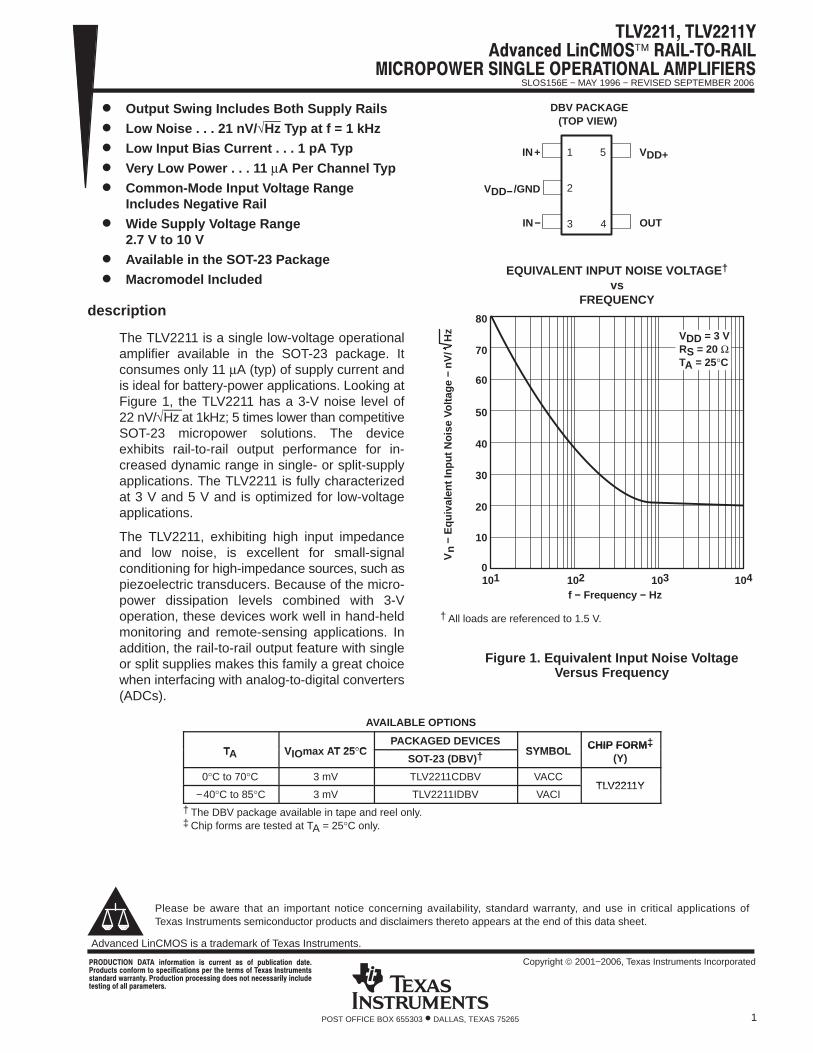
The TLV2211 is a single low-voltage operationalamplifier available in the SOT-23 package. Itconsumes only 11 µA (typ) of supply current andis ideal for battery-power applications. Looking atFigure 1, the TLV2211 has a 3-V noise level of22 nV/√Hz at 1kHz; 5 times lower than competitiveSOT-23 micropower solutions. The deviceexhibits rail-to-rail output performance for in-creased dynamic range in single- or split-supplyapplications. The TLV2211 is fully characterizedat 3 V and 5 V and is optimized for low-voltageapplications.
The TLV2211, exhibiting high input impedanceand low noise, is excellent for small-signalconditioning for high-impedance sources, such aspiezoelectric transducers. Because of the micro-power dissipation levels combined with 3-Voperation, these devices work well in hand-heldmonitoring and remote-sensing applications. Inaddition, the rail-to-rail output feature with singleor split supplies makes this family a great choicewhen interfacing with analog-to-digital converters(ADCs).
AVAILABLE OPTIONS
TA VIOmax AT 25 °CPACKAGED DEVICES
SYMBOL CHIP FORM‡TA VIOmax AT 25 °C
SOT-23 (DBV)†SYMBOL CHIP FORM‡
(Y)
0°C to 70°C 3 mV TLV2211CDBV VACCTLV2211Y
−40°C to 85°C 3 mV TLV2211IDBV VACITLV2211Y
† The DBV package available in tape and reel only.‡ Chip forms are tested at TA = 25°C only.
Please be aware that an important notice concerning availability, standard warranty, and use in critical applications ofTexas Instruments semiconductor products and disclaimers thereto appears at the end of this data sheet.
DBV PACKAGE(TOP VIEW)
5
43
1
2
IN−
VDD−/GND
IN+ VDD+
OUT
− E
quiv
alen
t Inp
ut N
oise
Vol
tage
−
f − Frequency − Hz
EQUIVALENT INPUT NOISE VOLTAGE †
vsFREQUENCY
Vn
nV/
Hz
40
30
20
0
60
50
10
VDD = 3 VRS = 20 ΩTA = 25°C
70
80
101 102 103 104
Figure 1. Equivalent Input Noise VoltageVersus Frequency
† All loads are referenced to 1.5 V.
!"#$! % &""$ % ! '&() $! $*"!& $% !!"# $! %' $!% '" $+ $"#% ! ,% %$"&#$%%$" -""$.* "!& $! '"! %%/ !% !$ %%"). )&$%$/ ! )) '"#$"%*
Copyright 2001−2006, Texas Instruments Incorporated
Advanced LinCMOS is a trademark of Texas Instruments.

SLOS156E − MAY 1996 − REVISED SEPTEMBER 2006
2 POST OFFICE BOX 655303 • DALLAS, TEXAS 75265
description (continued)
With a total area of 5.6mm2, the SOT-23 package only requires one-third the board space of the standard 8-pinSOIC package. This ultra-small package allows designers to place single amplifiers very close to the signalsource, minimizing noise pick-up from long PCB traces. TI has also taken special care to provide a pinout thatis optimized for board layout (see Figure 2). Both inputs are separated by GND to prevent coupling or leakagepaths. The OUT and IN− terminals are on the same end of the board to provide negative feedback. Finally, gainsetting resistors and decoupling capacitor are easily placed around the package.
VI VDD+
OUTIN−
VDD/GND
IN+C
RI
RF
GND
V+
VO
1
2
3
4
5
Figure 2. Typical Surface Mount Layout for a Fixed-Gain Noninverting Amplifier
SLOS156E − MAY 1996 − REVISED SEPTEMBER 2006
3POST OFFICE BOX 655303 • DALLAS, TEXAS 75265
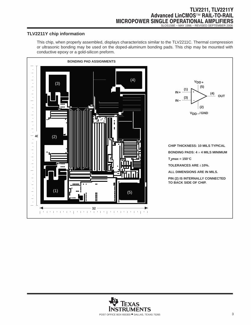
TLV2211Y chip information
This chip, when properly assembled, displays characteristics similar to the TLV2211C. Thermal compressionor ultrasonic bonding may be used on the doped-aluminum bonding pads. This chip may be mounted withconductive epoxy or a gold-silicon preform.
BONDING PAD ASSIGNMENTS
CHIP THICKNESS: 10 MILS TYPICAL
BONDING PADS: 4 × 4 MILS MINIMUM
TJmax = 150°C
TOLERANCES ARE ±10%.
ALL DIMENSIONS ARE IN MILS.
PIN (2) IS INTERNALLY CONNECTEDTO BACK SIDE OF CHIP.
+
−OUT
IN+
IN−
VDD+(5)
(1)
(3)(4)
(2)
VDD−/GND
40
(3)
(2)
(1) (5)
(4)
32

SLOS156E − MAY 1996 − REVISED SEPTEMBER 2006
4 POST OFFICE BOX 655303 • DALLAS, TEXAS 75265
equivalent schematic
Q3 Q6 Q9 Q12 Q14 Q16
Q2 Q5 Q7 Q8 Q10 Q11
D1
Q17Q15Q13
Q4Q1
R5
C1
VDD+
IN+
IN−
R3
R7
R1
R2
OUT
VDD−/GND
COMPONENT COUNT†
TransistorsDiodesResistorsCapacitors
23 611 2
† Includes both amplifiers and allESD, bias, and trim circuitry
R6
C2
D2R4
SLOS156E − MAY 1996 − REVISED SEPTEMBER 2006
5POST OFFICE BOX 655303 • DALLAS, TEXAS 75265
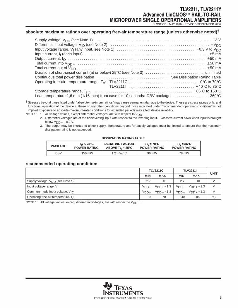
absolute maximum ratings over operating free-air temperature range (unless otherwise noted) †
Supply voltage, VDD (see Note 1) 12 V. . . . . . . . . . . . . . . . . . . . . . . . . . . . . . . . . . . . . . . . . . . . . . . . . . . . . . . . . . . . Differential input voltage, VID (see Note 2) ±VDD. . . . . . . . . . . . . . . . . . . . . . . . . . . . . . . . . . . . . . . . . . . . . . . . . . . Input voltage range, VI (any input, see Note 1) −0.3 V to VDD. . . . . . . . . . . . . . . . . . . . . . . . . . . . . . . . . . . . . . . . Input current, II (each input) ±5 mA. . . . . . . . . . . . . . . . . . . . . . . . . . . . . . . . . . . . . . . . . . . . . . . . . . . . . . . . . . . . . . . Output current, IO ±50 mA. . . . . . . . . . . . . . . . . . . . . . . . . . . . . . . . . . . . . . . . . . . . . . . . . . . . . . . . . . . . . . . . . . . . . . . Total current into VDD+ ±50 mA. . . . . . . . . . . . . . . . . . . . . . . . . . . . . . . . . . . . . . . . . . . . . . . . . . . . . . . . . . . . . . . . . . Total current out of VDD− ±50 mA. . . . . . . . . . . . . . . . . . . . . . . . . . . . . . . . . . . . . . . . . . . . . . . . . . . . . . . . . . . . . . . . Duration of short-circuit current (at or below) 25°C (see Note 3) unlimited. . . . . . . . . . . . . . . . . . . . . . . . . . . . . . Continuous total power dissipation See Dissipation Rating Table. . . . . . . . . . . . . . . . . . . . . . . . . . . . . . . . . . . . . Operating free-air temperature range, TA: TLV2211C 0°C to 70°C. . . . . . . . . . . . . . . . . . . . . . . . . . . . . . . . . . .
TLV2211I −40°C to 85°C. . . . . . . . . . . . . . . . . . . . . . . . . . . . . . . . . . Storage temperature range, Tstg −65°C to 150°C. . . . . . . . . . . . . . . . . . . . . . . . . . . . . . . . . . . . . . . . . . . . . . . . . . . Lead temperature 1,6 mm (1/16 inch) from case for 10 seconds: DBV package 260°C. . . . . . . . . . . . . . . . . .
† Stresses beyond those listed under “absolute maximum ratings” may cause permanent damage to the device. These are stress ratings only, andfunctional operation of the device at these or any other conditions beyond those indicated under “recommended operating conditions” is notimplied. Exposure to absolute-maximum-rated conditions for extended periods may affect device reliability.
NOTES: 1. All voltage values, except differential voltages, are with respect to VDD −.2. Differential voltages are at the noninverting input with respect to the inverting input. Excessive current flows when input is brought
below VDD− − 0.3 V.3. The output may be shorted to either supply. Temperature and /or supply voltages must be limited to ensure that the maximum
dissipation rating is not exceeded.
DISSIPATION RATING TABLE
PACKAGETA ≤ 25°C DERATING FACTOR TA = 70°C TA = 85°C
PACKAGETA ≤ 25 C
POWER RATINGDERATING FACTORABOVE TA = 25°C
TA = 70 CPOWER RATING
TA = 85 CPOWER RATING
DBV 150 mW 1.2 mW/°C 96 mW 78 mW
recommended operating conditions
TLV2211C TLV2211IUNIT
MIN MAX MIN MAXUNIT
Supply voltage, VDD 2.7 10 2.7 10 V
Input voltage range, VI VDD− VDD+ −1.3 VDD− VDD+ −1.3 V
Common-mode input voltage, VIC VDD− VDD+ −1.3 VDD− VDD+ −1.3 V
Operating free-air temperature, TA 0 70 −40 85 °C
NOTE 1: All voltage values, except differential voltages, are with respect to VDD −.
SLOS156E − MAY 1996 − REVISED SEPTEMBER 2006
6 POST OFFICE BOX 655303 • DALLAS, TEXAS 75265
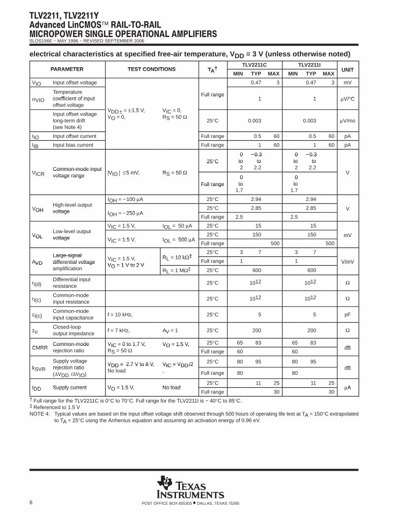
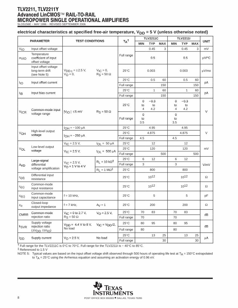
electrical characteristics at specified free-air temperature, V DD = 3 V (unless otherwise noted)
PARAMETER TEST CONDITIONS TA†TLV2211C TLV2211I
UNITPARAMETER TEST CONDITIONS TA†MIN TYP MAX MIN TYP MAX
UNIT
VIO Input offset voltage 0.47 3 0.47 3 mV
VIO
Temperature coefficient of input
Full range1 1 V/°CαVIO coefficient of input
offset voltageVDD = ±1.5 V, VIC = 0,
Full range1 1 µV/°C
Input offset voltagelong-term drift(see Note 4)
VDD± = ±1.5 V,VO = 0,
VIC = 0,RS = 50 Ω
25°C 0.003 0.003 µV/mo
IIO Input offset current Full range 0.5 60 0.5 60 pA
IIB Input bias current Full range 1 60 1 60 pA
0 −0.3 0 −0.325°C
0to
−0.3to
0to
−0.3to
VICRCommon-mode input
|VIO | ≤5 mV, RS = 50 Ω
25 C to2
to2.2
to2
to2.2
VVICRCommon-mode inputvoltage range |VIO | ≤5 mV, RS = 50 Ω
0 0Vvoltage range
Full range0to
0toFull range to
1.7to
1.7
High-level outputIOH = −100 µA 25°C 2.94 2.94
VOHHigh-level outputvoltage IOH = −250 A
25°C 2.85 2.85 VVOH voltage IOH = −250 µAFull range 2.5 2.5
V
Low-level outputVIC = 1.5 V, IOL = 50 µA 25°C 15 15
VOLLow-level outputvoltage VIC = 1.5 V, IOL = 500 A
25°C 150 150 mVVOL voltage VIC = 1.5 V, IOL = 500 µAFull range 500 500
mV
Large-signal V = 1.5 V, RL = 10 kه
25°C 3 7 3 7
AVD
Large-signal differential voltage
VIC = 1.5 V,VO = 1 V to 2 V
RL = 10 kهFull range 1 1 V/mVAVD differential voltage
amplificationVO = 1 V to 2 V
RL = 1 MΩ‡ 25°C 600 600
V/mV
ri(d)Differential inputresistance
25°C 1012 1012 Ω
ri(c)Common-mode input resistance
25°C 1012 1012 Ω
ci(c)Common-mode input capacitance
f = 10 kHz, 25°C 5 5 pF
zoClosed-loopoutput impedance
f = 7 kHz, AV = 1 25°C 200 200 Ω
CMRRCommon-mode VIC = 0 to 1.7 V, VO = 1.5 V, 25°C 65 83 65 83
dBCMRRCommon-moderejection ratio
VIC = 0 to 1.7 V,RS = 50 Ω
VO = 1.5 V, Full range 60 60
dB
kSVR
Supply voltage rejection ratio
VDD = 2.7 V to 8 V, VIC = VDD/2 25°C 80 95 80 95dBkSVR rejection ratio
(∆VDD /∆VIO)
VDD = 2.7 V to 8 V,No load
VIC = VDD/2, Full range 80 80
dB
IDD Supply current VO = 1.5 V, No load25°C 11 25 11 25
µAIDD Supply current VO = 1.5 V, No loadFull range 30 30
µA
† Full range for the TLV2211C is 0°C to 70°C. Full range for the TLV2211I is − 40°C to 85°C.‡ Referenced to 1.5 VNOTE 4: Typical values are based on the input offset voltage shift observed through 500 hours of operating life test at TA = 150°C extrapolated
to TA = 25°C using the Arrhenius equation and assuming an activation energy of 0.96 eV.
SLOS156E − MAY 1996 − REVISED SEPTEMBER 2006
7POST OFFICE BOX 655303 • DALLAS, TEXAS 75265
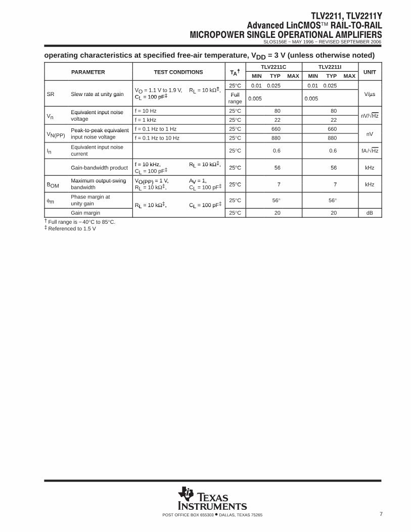
operating characteristics at specified free-air temperature, V DD = 3 V (unless otherwise noted)
PARAMETER TEST CONDITIONS TA†TLV2211C TLV2211I
UNITPARAMETER TEST CONDITIONS TA†MIN TYP MAX MIN TYP MAX
UNIT
25°C 0.01 0.025 0.01 0.025VO = 1.1 V to 1.9 V, RL = 10 kΩ‡,
25°C 0.01 0.025 0.01 0.025
SR Slew rate at unity gainVO = 1.1 V to 1.9 V,CL = 100 pF‡
RL = 10 kه,Full
0.005 0.005V/µsSR Slew rate at unity gain CL = 100 pF‡ Full
range 0.005 0.005V/µs
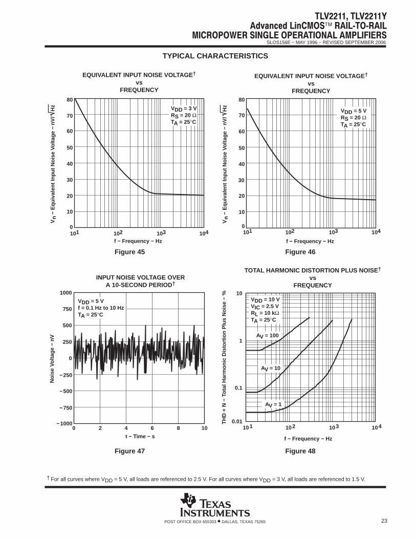
VnEquivalent input noise f = 10 Hz 25°C 80 80
nV/√HzVnEquivalent input noisevoltage f = 1 kHz 25°C 22 22
nV/√Hz
VN(PP)Peak-to-peak equivalent f = 0.1 Hz to 1 Hz 25°C 660 660
nVVN(PP)Peak-to-peak equivalentinput noise voltage f = 0.1 Hz to 10 Hz 25°C 880 880
nV
InEquivalent input noisecurrent
25°C 0.6 0.6 fA /√Hz
Gain-bandwidth productf = 10 kHz,
‡RL = 10 kΩ‡,
25°C 56 56 kHzGain-bandwidth productf = 10 kHz, CL = 100 pF‡
RL = 10 kΩ‡,25°C 56 56 kHz
BOMMaximum output-swing VO(PP) = 1 V,
‡AV = 1,
‡ 25°C 7 7 kHzBOMMaximum output-swingbandwidth
VO(PP) = 1 V, RL = 10 kه,
AV = 1,CL = 100 pF‡ 25°C 7 7 kHz
φmPhase margin atunity gain RL = 10 kΩ‡, CL = 100 pF‡
25°C 56° 56°
Gain margin
RL = 10 kΩ‡, CL = 100 pF‡
25°C 20 20 dB
† Full range is −40°C to 85°C.‡ Referenced to 1.5 V
SLOS156E − MAY 1996 − REVISED SEPTEMBER 2006
8 POST OFFICE BOX 655303 • DALLAS, TEXAS 75265
electrical characteristics at specified free-air temperature, V DD = 5 V (unless otherwise noted)
PARAMETER TEST CONDITIONS TA†TLV2211C TLV2211I
UNITPARAMETER TEST CONDITIONS TA†MIN TYP MAX MIN TYP MAX
UNIT
VIO Input offset voltage 0.45 3 0.45 3 mV
αVIO
Temperature coefficient of input
Full range0.5 0.5 µV/°CαVIO coefficient of input
offset voltage
Full range0.5 0.5 µV/°C
Input offset voltagelong-term drift(see Note 5)
VDD± = ±2.5 V,VO = 0,
VIC = 0, RS = 50 Ω
25°C 0.003 0.003 µV/mo
IIO Input offset current
VO = 0, RS = 50
25°C 0.5 60 0.5 60pAIIO Input offset current
Full range 150 150pA
IIB Input bias current25°C 1 60 1 60
pAIIB Input bias currentFull range 150 150
pA
0 −0.3 0 −0.325°C
0to
−0.3to
0to
−0.3to
VICRCommon-mode input |VIO | ≤5 mV RS = 50 Ω
25 C to4
to4.2
to4
to4.2
VVICRCommon-mode inputvoltage range
|VIO | ≤5 mV RS = 50 Ω0 0
Vvoltage range
Full range0to
0toFull range to
3.5to
3.5
High-level outputIOH = −100 µA 25°C 4.95 4.95
VOHHigh-level outputvoltage IOH = −250 µA
25°C 4.875 4.875 VVOH voltage IOH = −250 µAFull range 4.5 4.5
V
Low-level outputVIC = 2.5 V, IOL = 50 µA 25°C 12 12
VOLLow-level outputvoltage VIC = 2.5 V, IOL = 500 µA
25°C 120 120 mVVOL voltage VIC = 2.5 V, IOL = 500 µAFull range 500 500
mV
Large-signalVIC = 2.5 V, RL = 10 kه
25°C 6 12 6 12
AVD
Large-signaldifferentialvoltage amplification
VIC = 2.5 V,VO = 1 V to 4 V
RL = 10 kهFull range 3 3 V/mVAVD differential
voltage amplificationVO = 1 V to 4 V
RL = 1 MΩ‡ 25°C 800 800
V/mV
ri(d)Differential inputresistance
25°C 1012 1012 Ω
ri(c)Common-mode input resistance
25°C 1012 1012 Ω
ci(c)Common-mode input capacitance
f = 10 kHz, 25°C 5 5 pF
zoClosed-loopoutput impedance
f = 7 kHz, AV = 1 25°C 200 200 Ω
CMRRCommon-mode VIC = 0 to 2.7 V, VO = 2.5 V, 25°C 70 83 70 83
dBCMRRCommon-moderejection ratio
VIC = 0 to 2.7 V,RS = 50 Ω
VO = 2.5 V,Full range 70 70
dB
kSVR
Supply voltage rejection ratio
VDD = 4.4 V to 8 V, VIC = VDD/2, 25°C 80 95 80 95dBkSVR rejection ratio
(∆VDD /∆VIO)
VDD = 4.4 V to 8 V,No load
VIC = VDD/2,
Full range 80 80dB
IDD Supply current VO = 2.5 V, No load25°C 13 25 13 25
µAIDD Supply current VO = 2.5 V, No loadFull range 30 30
µA
† Full range for the TLV2211C is 0°C to 70°C. Full range for the TLV2211I is − 40°C to 85°C.‡ Referenced to 1.5 VNOTE 5: Typical values are based on the input offset voltage shift observed through 500 hours of operating life test at TA = 150°C extrapolated
to TA = 25°C using the Arrhenius equation and assuming an activation energy of 0.96 eV.

SLOS156E − MAY 1996 − REVISED SEPTEMBER 2006
9POST OFFICE BOX 655303 • DALLAS, TEXAS 75265
operating characteristics at specified free-air temperature, V DD = 5 V (unless otherwise noted)
PARAMETER TEST CONDITIONS TA†TLV2211C TLV2211I
UNITPARAMETER TEST CONDITIONS TA†MIN TYP MAX MIN TYP MAX
UNIT
25°C 0.01 0.025 0.01 0.025VO = 1.5 V to 3.5 V, RL = 10 kΩ‡,
25°C 0.01 0.025 0.01 0.025
SR Slew rate at unity gainVO = 1.5 V to 3.5 V,CL = 100 pF‡
RL = 10 kه,Full
0.005 0.005V/µsSR Slew rate at unity gain CL = 100 pF‡ Full
range 0.005 0.005V/µs
VnEquivalent input noise f = 10 Hz 25°C 72 72
nV/√HzVnEquivalent input noisevoltage f = 1 kHz 25°C 21 21
nV/√Hz
VN(PP)Peak-to-peak equivalent f = 0.1 Hz to 1 Hz 25°C 600 600
nVVN(PP)Peak-to-peak equivalentinput noise voltage f = 0.1 Hz to 10 Hz 25°C 800 800
nV
InEquivalent input noisecurrent
25°C 0.6 0.6 fA /√Hz
Gain-bandwidth productf = 10 kHz,
‡RL = 10 kΩ‡,
25°C 65 65 kHzGain-bandwidth productf = 10 kHz, CL = 100 pF‡
RL = 10 kΩ‡,25°C 65 65 kHz
BOMMaximum output-swing VO(PP) = 2 V,
‡AV = 1,
‡ 25°C 7 7 kHzBOMMaximum output-swingbandwidth
VO(PP) = 2 V, RL = 10 kه,
AV = 1,CL = 100 pF‡ 25°C 7 7 kHz
φmPhase margin atunity gain RL = 10 kΩ‡, CL = 100 pF‡
25°C 56° 56°
Gain margin
RL = 10 kΩ‡, CL = 100 pF‡
25°C 22 22 dB
† Full range is −40°C to 85°C.‡ Referenced to 1.5 V
electrical characteristics at V DD = 3 V, TA = 25°C (unless otherwise noted)
PARAMETER TEST CONDITIONSTLV2211Y
UNITPARAMETER TEST CONDITIONSMIN TYP MAX
UNIT
VIO Input offset voltageVDD = ±1.5 V, VO = 0, VIC = 0,
0.47 mV
IIO Input offset currentVDD± = ±1.5 V,RS = 50 Ω
VO = 0, VIC = 0,0.5 60 pA
IIB Input bias currentRS = 50 Ω
1 60 pA
−0.3VICR Common-mode input voltage range | VIO | ≤5 mV, RS = 50 Ω
−0.3to 2.2 VVICR Common-mode input voltage range | VIO | ≤5 mV, RS = 50 Ω to 2.2 V
VOH High-level output voltageIOH = −100 µA 2.94
VVOH High-level output voltageIOH = −200 µA 2.85
V
VOL Low-level output voltageVIC = 0, IOL = 50 µA 15
mVVOL Low-level output voltageVIC = 0, IOL = 500 µA 150
mV
AVDLarge-signal differential
VIC = 1.5 V, VO = 1 V to 2 VRL = 10 kن 7
V/mVAVDLarge-signal differentialvoltage amplification VIC = 1.5 V, VO = 1 V to 2 V
RL = 1 Mن 600V/mV
ri(d) Differential input resistance 1012 Ω
ri(c) Common-mode input resistance 1012 Ω
ci(c) Common-mode input capacitance f = 10 kHz 5 pF
zo Closed-loop output impedance f = 7 kHz, AV = 1 200 Ω
CMRR Common-mode rejection ratio VIC = 0 to 1.7 V, VO = 1.5 V, RS = 50 Ω 83 dB
kSVRSupply voltage rejection ratio
VDD = 2.7 V to 8 V, VIC = VDD/2, No load 95 dBkSVRSupply voltage rejection ratio(∆VDD/∆VIO) VDD = 2.7 V to 8 V, VIC = VDD/2, No load 95 dB
IDD Supply current VO = 1.5 V, No load 11 µA
† Referenced to 1.5 V

SLOS156E − MAY 1996 − REVISED SEPTEMBER 2006
10 POST OFFICE BOX 655303 • DALLAS, TEXAS 75265
electrical characteristics at V DD = 5 V, TA = 25°C (unless otherwise noted)
PARAMETER TEST CONDITIONSTLV2211Y
UNITPARAMETER TEST CONDITIONSMIN TYP MAX
UNIT
VIO Input offset voltageVDD± = ±2.5 V, VIC = 0, VO = 0,
0.45 mV
IIO Input offset currentVDD± = ±2.5 V,RS = 50 Ω
VIC = 0, VO = 0,0.5 60 pA
IIB Input bias currentRS = 50 Ω
1 60 pA
−0.3VICR Common-mode input voltage range | VIO | ≤5 mV, RS = 50 Ω
−0.3to 4.2 VVICR Common-mode input voltage range | VIO | ≤5 mV, RS = 50 Ω to 4.2 V
VOH High-level output voltageIOH = −100 µA 4.95
VVOH High-level output voltageIOH = −250 µA 4.875
V
VOL Low-level output voltageVIC = 2.5 V, IOL = 50 µA 12
mVVOL Low-level output voltageVIC = 2.5 V, IOL = 500 µA 120
mV
AVDLarge-signal differential
VIC = 2.5 V, VO = 1 V to 4 VRL = 10 kن 12
V/mVAVDLarge-signal differentialvoltage amplification VIC = 2.5 V, VO = 1 V to 4 V
RL = 1 Mن 800V/mV
ri(d) Differential input resistance 1012 Ω
ri(c) Common-mode input resistance 1012 Ω
ci(c) Common-mode input capacitance f = 10 kHz 5 pF
zo Closed-loop output impedance f = 7 kHz, AV = 1 200 Ω
CMRR Common-mode rejection ratio VIC = 0 to 2.7 V, VO = 2.5 V, RS = 50 Ω 83 dB
kSVRSupply voltage rejection ratio
VDD = 4.4 V to 8 V, VIC = VDD/2, No load 95 dBkSVRSupply voltage rejection ratio(∆VDD/∆VIO) VDD = 4.4 V to 8 V, VIC = VDD/2, No load 95 dB
IDD Supply current VO = 2.5 V, No load 13 µA
† Referenced to 1.5 V
SLOS156E − MAY 1996 − REVISED SEPTEMBER 2006
11POST OFFICE BOX 655303 • DALLAS, TEXAS 75265
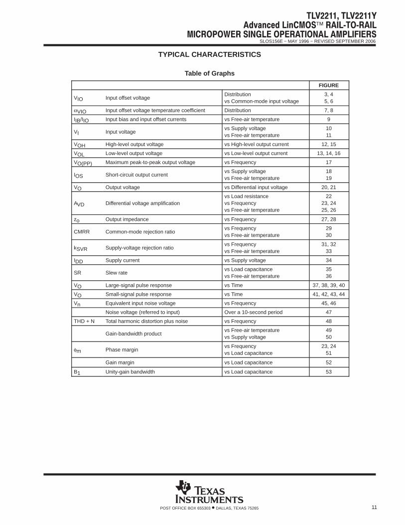
TYPICAL CHARACTERISTICS
Table of Graphs
FIGURE
VIO Input offset voltageDistributionvs Common-mode input voltage
3, 45, 6
αVIO Input offset voltage temperature coefficient Distribution 7, 8
IIB/IIO Input bias and input offset currents vs Free-air temperature 9
VI Input voltagevs Supply voltagevs Free-air temperature
1011
VOH High-level output voltage vs High-level output current 12, 15
VOL Low-level output voltage vs Low-level output current 13, 14, 16
VO(PP) Maximum peak-to-peak output voltage vs Frequency 17
IOS Short-circuit output currentvs Supply voltagevs Free-air temperature
1819
VO Output voltage vs Differential input voltage 20, 21
AVD Differential voltage amplificationvs Load resistancevs Frequencyvs Free-air temperature
2223, 2425, 26
zo Output impedance vs Frequency 27, 28
CMRR Common-mode rejection ratiovs Frequencyvs Free-air temperature
2930
kSVR Supply-voltage rejection ratiovs Frequencyvs Free-air temperature
31, 3233
IDD Supply current vs Supply voltage 34
SR Slew ratevs Load capacitancevs Free-air temperature
3536
VO Large-signal pulse response vs Time 37, 38, 39, 40
VO Small-signal pulse response vs Time 41, 42, 43, 44
Vn Equivalent input noise voltage vs Frequency 45, 46
Noise voltage (referred to input) Over a 10-second period 47
THD + N Total harmonic distortion plus noise vs Frequency 48
Gain-bandwidth productvs Free-air temperaturevs Supply voltage
4950
φm Phase marginvs Frequencyvs Load capacitance
23, 2451
Gain margin vs Load capacitance 52
B1 Unity-gain bandwidth vs Load capacitance 53

SLOS156E − MAY 1996 − REVISED SEPTEMBER 2006
12 POST OFFICE BOX 655303 • DALLAS, TEXAS 75265
TYPICAL CHARACTERISTICS
Figure 3
Pre
cent
age
of A
mpl
ifier
s −
%
DISTRIBUTION OF TLV2211INPUT OFFSET VOLTAGE
VIO − Input Offset Voltage − mV
15
10
5
0
20
25
30
−1.5 −1 −0.5 0 0.5 1 1.5
376 Amplifiers From 1 Wafer LotVDD = ±1.5 VTA = 25°C
Figure 4
Pre
cent
age
of A
mpl
ifier
s −
%
DISTRIBUTION OF TLV2211INPUT OFFSET VOLTAGE
VIO − Input Offset Voltage − mV
15
10
5
0
20
25
30
−1.5 −1 −0.5 0 0.5 1 1.5
376 Amplifiers From 1 Wafer LotVDD = ±2.5 VTA = 25°C
Figure 5
− In
put O
ffset
Vol
tage
− m
V
INPUT OFFSET VOLTAGE†
vsCOMMON-MODE INPUT VOLTAGE
ÁÁÁÁV
IO
VIC − Common-Mode Input Voltage − V
1
0.8
0.6
0.4
0.2
0
−0.2
−0.4
−0.6
−0.8
−1−1 0 1 2
VDD = 3 VRS = 50 ΩTA = 25°C
3
Figure 6
− In
put O
ffset
Vol
tage
− m
V
INPUT OFFSET VOLTAGE†
vsCOMMON-MODE INPUT VOLTAGE
ÁÁÁÁÁÁ
VIO
VIC − Common-Mode Input Voltage − V
1
0.8
0.6
0.4
0.2
0
−0.2
−0.4
−0.6
−0.8
−1−1 0 1 2 3 4 5
VDD = 5 VRS = 50 ΩTA = 25°C
† For all curves where VDD = 5 V, all loads are referenced to 2.5 V. For all curves where VDD = 3 V, all loads are referenced to 1.5 V.
SLOS156E − MAY 1996 − REVISED SEPTEMBER 2006
13POST OFFICE BOX 655303 • DALLAS, TEXAS 75265
TYPICAL CHARACTERISTICS
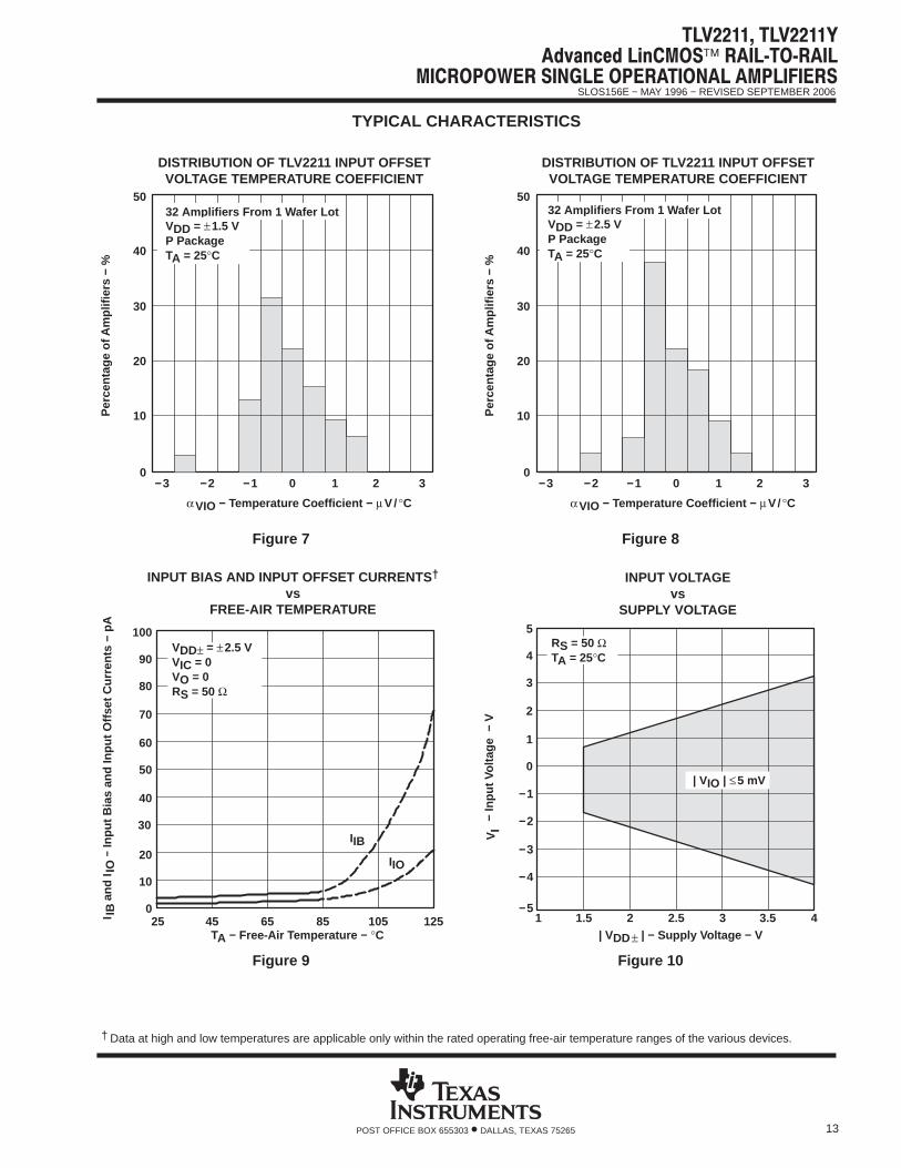
Figure 7
DISTRIBUTION OF TLV2211 INPUT OFFSETVOLTAGE TEMPERATURE COEFFICIENT
Per
cent
age
of A
mpl
ifier
s −
%
αVIO − Temperature Coefficient − µV/ °C
30
20
10
0
40
50
−3 −2 −1 0 1 2 3
32 Amplifiers From 1 Wafer LotVDD = ±1.5 VP PackageTA = 25°C
Figure 8
DISTRIBUTION OF TLV2211 INPUT OFFSETVOLTAGE TEMPERATURE COEFFICIENT
Per
cent
age
of A
mpl
ifier
s −
%αVIO − Temperature Coefficient − µV/ °C
30
20
10
0
40
50
−3 −2 −1 0 1 2 3
32 Amplifiers From 1 Wafer LotVDD = ±2.5 VP PackageTA = 25°C
Figure 9
IIB a
nd II
O −
Inpu
t Bia
s an
d In
put O
ffset
Cur
rent
s −
pA
INPUT BIAS AND INPUT OFFSET CURRENTS †
vsFREE-AIR TEMPERATURE
I IB
I IO
TA − Free-Air Temperature − °C
50
40
20
10
0
90
30
25 45 65 85
70
60
80
100
105 125
IIB
IIO
VDD± = ±2.5 VVIC = 0 VO = 0RS = 50 Ω
Figure 10
0
4
1 1.5 2 2.5
− In
put V
olta
ge −
V
2
1
3
INPUT VOLTAGEvs
SUPPLY VOLTAGE5
3 3.5 4
−1
−2
−3
−4
−5
RS = 50 ΩTA = 25°C
| VIO | ≤5 mV
ÁÁÁÁ
VI
| VDD± | − Supply Voltage − V
† Data at high and low temperatures are applicable only within the rated operating free-air temperature ranges of the various devices.

SLOS156E − MAY 1996 − REVISED SEPTEMBER 2006
14 POST OFFICE BOX 655303 • DALLAS, TEXAS 75265
TYPICAL CHARACTERISTICS
Figure 11
− In
put V
olta
ge −
V
INPUT VOLTAGE†‡
vsFREE-AIR TEMPERATURE
ÁÁÁVI
TA − Free-Air Temperature − °C
2
1
0
3
4
5
−1−55 −35 −15 5 25 45 65 85
| VIO | ≤5 mV
VDD = 5 V
105 125
Figure 12
− H
igh-
Leve
l Out
put V
olta
ge −
V
HIGH-LEVEL OUTPUT VOLTAGE †‡
vsHIGH-LEVEL OUTPUT CURRENT
ÁÁÁÁÁÁ
V OH
| IOH | − High-Level Output Current − µA
2
1.5
1
00 200 400
2.5
3
600 800
VDD = 3 V
TA = −40°C
0.5
TA = 25°C
TA = 85°C
TA = 125°C
Figure 13
− Lo
w-L
evel
Out
put V
olta
ge −
V
LOW-LEVEL OUTPUT VOLTAGE ‡
vsLOW-LEVEL OUTPUT CURRENT
ÁÁÁÁ
V OL
IOL − Low-Level Output Current − mA
0.6
0.4
0.2
00 1 2 3
0.8
1
1.2
4 5
VDD = 3 VTA = 25°C
VIC = 0VIC = 0.75 V
VIC = 1.5 V
Figure 14
− Lo
w-L
evel
Out
put V
olta
ge −
V
LOW-LEVEL OUTPUT VOLTAGE †‡
vsLOW-LEVEL OUTPUT CURRENT
ÁÁÁÁÁÁ
V OL
IOL − Low-Level Output Current − mA
0.4
0.2
1.2
00 1 2 3
0.8
0.6
1
1.4
4 5
TA = 85°C
TA = − 40°C
TA = 25°C
TA = 125°C
VDD = 3 VVIC = 1.5 V
† Data at high and low temperatures are applicable only within the rated operating free-air temperature ranges of the various devices.‡ For all curves where VDD = 5 V, all loads are referenced to 2.5 V. For all curves where VDD = 3 V, all loads are referenced to 1.5 V.
SLOS156E − MAY 1996 − REVISED SEPTEMBER 2006
15POST OFFICE BOX 655303 • DALLAS, TEXAS 75265
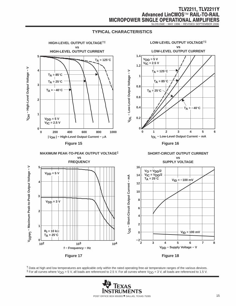
TYPICAL CHARACTERISTICS
Figure 15
− H
igh-
Leve
l Out
put V
olta
ge −
V
HIGH-LEVEL OUTPUT VOLTAGE †‡
vsHIGH-LEVEL OUTPUT CURRENT
ÁÁÁÁ
V OH
| IOH | − High-Level Output Current − µA
3
2
1
00 200 400 600
4
5
800 1000
TA = −40°C
TA = 25°C
TA = 125°C
TA = 85°C
VDD = 5 VVIC = 2.5 V
Figure 16
− Lo
w-L
evel
Out
put V
olta
ge −
V
LOW-LEVEL OUTPUT VOLTAGE †‡
vsLOW-LEVEL OUTPUT CURRENT
ÁÁÁÁV
OL
IOL − Low-Level Output Current − mA
0.6
0.4
0.2
00 1 2 3
1
1.2
1.4
4 5 6
0.8
VDD = 5 VVIC = 2.5 V
TA = −40°C
TA = 85°C
TA = 25°C
TA = 125°C
Figure 17
− M
axim
um P
eak-
to-P
eak
Out
put V
olta
ge −
V
f − Frequency − Hz
MAXIMUM PEAK-TO-PEAK OUTPUT VOLTAGE ‡
vsFREQUENCY
ÁÁÁÁÁÁ
VO
(PP
)
4
2
1
5
3
0
RI = 10 kΩTA = 25°C
VDD = 5 V
VDD = 3 V
102 103 104
Figure 18
− S
hort
-Circ
uit O
utpu
t Cur
rent
− m
A
SHORT-CIRCUIT OUTPUT CURRENTvs
SUPPLY VOLTAGE
I OS
VDD − Supply Voltage − V
10
6
2
2 3 4 5
14
16
6 7 8
12
8
4
0
−2
VID = −100 mV
VID = 100 mV
VO = VDD/2VIC = VDD/2TA = 25°C
† Data at high and low temperatures are applicable only within the rated operating free-air temperature ranges of the various devices.‡ For all curves where VDD = 5 V, all loads are referenced to 2.5 V. For all curves where VDD = 3 V, all loads are referenced to 1.5 V.
SLOS156E − MAY 1996 − REVISED SEPTEMBER 2006
16 POST OFFICE BOX 655303 • DALLAS, TEXAS 75265
TYPICAL CHARACTERISTICS
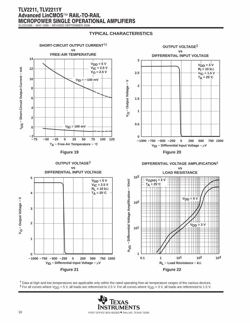
Figure 19
− S
hort
-Circ
uit O
utpu
t Cur
rent
− m
A
SHORT-CIRCUIT OUTPUT CURRENT†‡
vsFREE-AIR TEMPERATURE
I OS
TA − Free-Air Temperature − °C
14
10
6
4
2
0
−2−50 −25 0 25 50 75 100−75 125
8
12
VID = −100 mV
VID = 100 mV
VDD = 5 VVIC = 2.5 VVO = 2.5 V
Figure 20
0
0.5
1
1.5
2
2.5
3
−250−500−750−1000 250 500 750 10000
VDD = 3 VRI = 10 kΩVIC = 1.5 VTA = 25°C
OUTPUT VOLTAGE‡
vsDIFFERENTIAL INPUT VOLTAGE
VID − Differential Input Voltage − µV
− O
utpu
t Vol
tage
− V
VO
Figure 21
VID − Differential Input Voltage − µV
− O
utpu
t Vol
tage
− V
VO
0
1
3
2
4
5VDD = 5 VVIC = 2.5 VRL = 10 kΩTA = 25°C
−250−500−750−1000 250 500 750 10000
OUTPUT VOLTAGE‡
vsDIFFERENTIAL INPUT VOLTAGE
Figure 22
DIFFERENTIAL VOLTAGE AMPLIFICATION ‡
vsLOAD RESISTANCE
RL − Load Resistance − k Ω
− D
iffer
entia
l Vol
tage
Am
plifi
catio
n −
V/m
V
ÁÁÁÁ
AV
D
103
102
101
10.1 1 101 102 103
VO(PP) = 2 VTA = 25°C
VDD = 5 V
VDD = 3 V
† Data at high and low temperatures are applicable only within the rated operating free-air temperature ranges of the various devices.‡ For all curves where VDD = 5 V, all loads are referenced to 2.5 V. For all curves where VDD = 3 V, all loads are referenced to 1.5 V.
SLOS156E − MAY 1996 − REVISED SEPTEMBER 2006
17POST OFFICE BOX 655303 • DALLAS, TEXAS 75265
TYPICAL CHARACTERISTICS
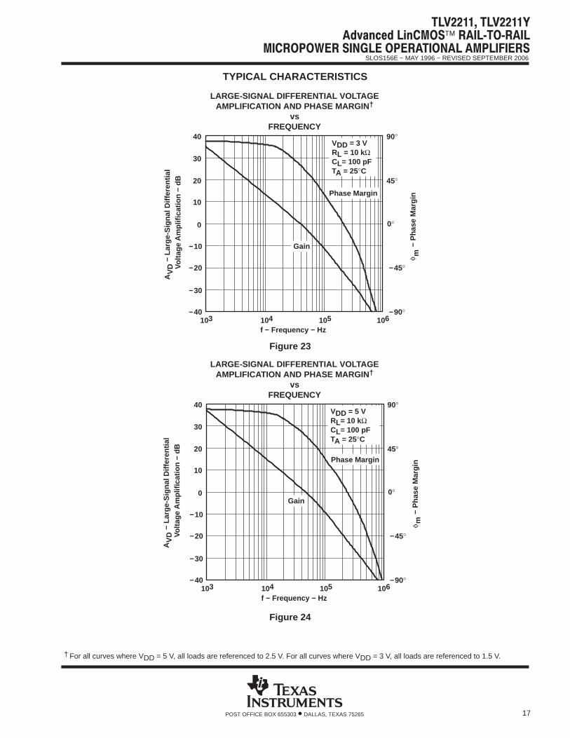
om −
Pha
se M
argi
n φ m
f − Frequency − Hz
LARGE-SIGNAL DIFFERENTIAL VOLTAGEAMPLIFICATION AND PHASE MARGIN †
vsFREQUENCY
AV
D −
Lar
ge-S
igna
l Diff
eren
tial
ÁÁÁÁA
VD V
olta
ge A
mpl
ifica
tion
− dB
40
30
20
10
0
−10
−20
−30
−40103 104 105 106
90°
45°
0°
−45°
−90°
VDD = 3 VRL = 10 kΩCL= 100 pFTA = 25°C
Phase Margin
Gain
Figure 23
om −
Pha
se M
argi
n φ m
f − Frequency − Hz
LARGE-SIGNAL DIFFERENTIAL VOLTAGEAMPLIFICATION AND PHASE MARGIN †
vsFREQUENCY
AV
D −
Lar
ge-S
igna
l Diff
eren
tial
ÁÁÁÁ
AV
D Vol
tage
Am
plifi
catio
n −
dB
40
30
20
10
0
−10
−20
−30
−40103 104 105 106
90°
45°
0°
−45°
−90°
VDD = 5 VRL= 10 kΩCL= 100 pFTA = 25°C
Phase Margin
Gain
Figure 24
† For all curves where VDD = 5 V, all loads are referenced to 2.5 V. For all curves where VDD = 3 V, all loads are referenced to 1.5 V.
SLOS156E − MAY 1996 − REVISED SEPTEMBER 2006
18 POST OFFICE BOX 655303 • DALLAS, TEXAS 75265
TYPICAL CHARACTERISTICS
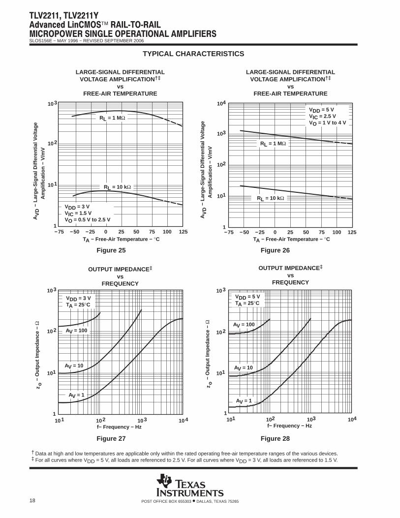
Figure 25
LARGE-SIGNAL DIFFERENTIALVOLTAGE AMPLIFICATION †‡
vsFREE-AIR TEMPERATURE
TA − Free-Air Temperature − °C
− La
rge-
Sig
nal D
iffer
entia
l Vol
tage
A
VD
Am
plifi
catio
n −
V/m
V
−50 −25 0 25 50 75 100
RL = 10 kΩ
RL = 1 MΩ
103
102
101
1
VDD = 3 VVIC = 1.5 VVO = 0.5 V to 2.5 V
−75 125
Figure 26
LARGE-SIGNAL DIFFERENTIALVOLTAGE AMPLIFICATION †‡
vsFREE-AIR TEMPERATURE
TA − Free-Air Temperature − °C
− La
rge-
Sig
nal D
iffer
entia
l Vol
tage
A
VD
Am
plifi
catio
n −
V/m
V
104
103
102
101
1−75 −50 −25 0 25 50 75 100 125
VDD = 5 VVIC = 2.5 VVO = 1 V to 4 V
RL = 1 MΩ
RL = 10 kΩ
Figure 27
− O
utpu
t Im
peda
nce
−
f− Frequency − Hz
OUTPUT IMPEDANCE‡
vsFREQUENCY
Ωz
o
101 102 103 104
AV = 100
AV = 10
AV = 1
VDD = 3 VTA = 25°C
103
102
101
1
Figure 28
− O
utpu
t Im
peda
nce
−
f− Frequency − Hz
OUTPUT IMPEDANCE‡
vsFREQUENCY
Ωz
o
AV = 100
AV = 1
VDD = 5 VTA = 25°C
1101 102 103 104
AV = 10
103
102
101
† Data at high and low temperatures are applicable only within the rated operating free-air temperature ranges of the various devices.‡ For all curves where VDD = 5 V, all loads are referenced to 2.5 V. For all curves where VDD = 3 V, all loads are referenced to 1.5 V.
SLOS156E − MAY 1996 − REVISED SEPTEMBER 2006
19POST OFFICE BOX 655303 • DALLAS, TEXAS 75265
TYPICAL CHARACTERISTICS
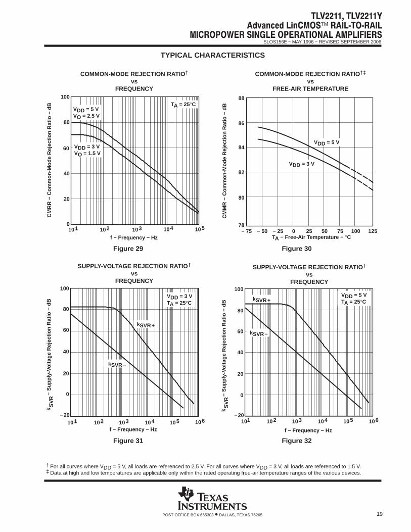
Figure 29
CM
RR
− C
omm
on-M
ode
Rej
ectio
n R
atio
− d
B
f − Frequency − Hz
COMMON-MODE REJECTION RATIO†
vsFREQUENCY
80
40
20
0
100
60
101 102 103 104 105
VDD = 5 VVO = 2.5 V
VDD = 3 VVO = 1.5 V
TA = 25°C
Figure 30
CM
MR
− C
omm
on-M
ode
Rej
ectio
n R
atio
− d
B
COMMON-MODE REJECTION RATIO†‡
vsFREE-AIR TEMPERATURE
TA − Free-Air Temperature − °C
82
80
78
86
84
88
VDD = 5 V
VDD = 3 V
− 50 − 25 0 25 50 75 100− 75 125
Figure 31
− S
uppl
y-Vo
ltage
Rej
ectio
n R
atio
− d
B
f − Frequency − Hz
SUPPLY-VOLTAGE REJECTION RATIO †
vsFREQUENCY
ÁÁÁÁk
SV
R
60
40
20
100
80
0
−20
kSVR−
kSVR+
101 102 103 104 105 106
VDD = 3 VTA = 25°C
Figure 32
− S
uppl
y-Vo
ltage
Rej
ectio
n R
atio
− d
B
f − Frequency − Hz
SUPPLY-VOLTAGE REJECTION RATIO †
vsFREQUENCY
ÁÁÁÁÁÁ
kS
VR
100
80
60
40
20
0
−20101 102 103 104 105 106
VDD = 5 VTA = 25°C
kSVR−
kSVR+
‡ Data at high and low temperatures are applicable only within the rated operating free-air temperature ranges of the various devices.
† For all curves where VDD = 5 V, all loads are referenced to 2.5 V. For all curves where VDD = 3 V, all loads are referenced to 1.5 V.
SLOS156E − MAY 1996 − REVISED SEPTEMBER 2006
20 POST OFFICE BOX 655303 • DALLAS, TEXAS 75265
TYPICAL CHARACTERISTICS
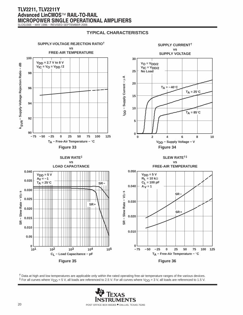
Figure 33
− S
uppl
y-Vo
ltage
Rej
ectio
n R
atio
− d
B
SUPPLY-VOLTAGE REJECTION RATIO †
vsFREE-AIR TEMPERATURE
ÁÁÁ
kS
VR
TA − Free-Air Temperature − °C
94
92
90
98
100
−50 −25 0 25 50 75 100
VDD = 2.7 V to 8 VVIC = VO = VDD /2
125−75
96
Figure 34
− S
uppl
y C
urre
nt −
A
µ
ÁÁÁÁÁÁ
I DD
VDD − Supply Voltage − V
SUPPLY CURRENT†
vsSUPPLY VOLTAGE
VO = VDD/2VIC = VDD/2 No Load
TA = 25°C
TA = 85°C
TA = −40°C
15
10
5
0 2 4 6
20
25
30
8 100
Figure 35
SR
− S
lew
Rat
e −
SLEW RATE‡
vsLOAD CAPACITANCE
CL − Load Capacitance − pF
0.030
0.05
0.020
0
0.040
0.025
0.035
0.010
0.015
101 102 103 104 105
VDD = 5 VAV = −1TA = 25°C SR−
SR+
sµ
V/
Figure 36
SLEW RATE†‡
vsFREE-AIR TEMPERATURE
TA − Free-Air Temperature − °C
SR
− S
lew
Rat
e −
sµ
V/
0.020
0.010
0
0.030
0.040
0.050
−50 −25 0 25 50 75 100
SR−
SR+
VDD = 5 VRL = 10 kΩCL = 100 pFA V = 1
−75 125
† Data at high and low temperatures are applicable only within the rated operating free-air temperature ranges of the various devices.‡ For all curves where VDD = 5 V, all loads are referenced to 2.5 V. For all curves where VDD = 3 V, all loads are referenced to 1.5 V.

SLOS156E − MAY 1996 − REVISED SEPTEMBER 2006
21POST OFFICE BOX 655303 • DALLAS, TEXAS 75265
TYPICAL CHARACTERISTICS
Figure 37
− O
utpu
t Vol
tage
− V
INVERTING LARGE-SIGNAL PULSERESPONSE†
VO
t − Time − µs
1.5
1
0.5
00 50 100 150 200 250 300
2
2.5
3
350 400 450 500
A V = −1TA = 25°C
VDD = 3 VRL = 10 kΩCL = 100 pF
Figure 38
INVERTING LARGE-SIGNAL PULSERESPONSE†
t − Time − µs −
Out
put V
olta
ge −
VV
O
2
1
00 50 100 150 200 250 300
3
4
5
350 400 450 500
VDD = 5 VRL = 10 kΩCL = 100 pFAV = −1TA = 25°C
Figure 39
VOLTAGE-FOLLOWER LARGE-SIGNALPULSE RESPONSE†
− O
utpu
t Vol
tage
− V
VO
t − Time − µs
2
1
00 100 200 300 400 500 600
3
4
5
700 800 900 1000
VDD = 5 VRL = 10 kΩCL = 100 pFAV = 1TA = 25°C
Figure 40
VOLTAGE-FOLLOWER LARGE-SIGNALPULSE RESPONSE†
− O
utpu
t Vol
tage
− V
VO
t − Time − µs
2
1
00 100 200 300 400 500
3
4
5VDD = 5 VCL = 100 pFAV = 1TA = 25°C
RL = 10 kΩTied to 2.5 V
RL = 100 kΩTied to 2.5 V
RL = 10 kΩTied to 0 V
† For all curves where VDD = 5 V, all loads are referenced to 2.5 V. For all curves where VDD = 3 V, all loads are referenced to 1.5 V.
SLOS156E − MAY 1996 − REVISED SEPTEMBER 2006
22 POST OFFICE BOX 655303 • DALLAS, TEXAS 75265
TYPICAL CHARACTERISTICS
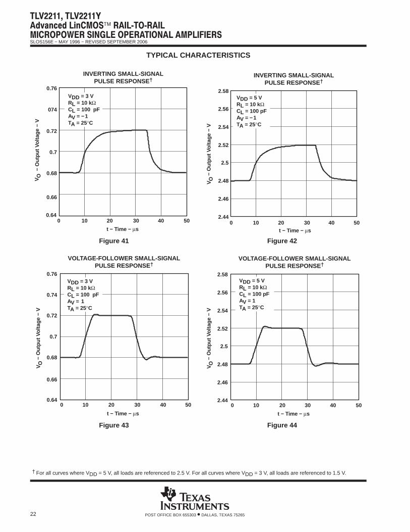
Figure 41
INVERTING SMALL-SIGNALPULSE RESPONSE†
− O
utpu
t Vol
tage
− V
VO
t − Time − µs
0.68
0.66
074
0.640 10 20 30
0.7
0.72
0.76
40 50
VDD = 3 VRL = 10 kΩCL = 100 pFAV = −1TA = 25°C
Figure 42
VO
− O
utpu
t Vol
tage
− V
INVERTING SMALL-SIGNALPULSE RESPONSE†
VO
t − Time − µs
2.5
2.46
2.440 10 20 30
2.52
2.56
2.58
40 50
VDD = 5 VRL = 10 kΩCL = 100 pFAV = −1TA = 25°C
2.48
2.54
Figure 43
VOLTAGE-FOLLOWER SMALL-SIGNALPULSE RESPONSE†
VO
− O
utpu
t Vol
tage
− V
VO
t − Time − µs
VDD = 3 VRL = 10 kΩCL = 100 pFAV = 1TA = 25°C
0.7
0.68
0.66
0.640 10 20 30 40 50
0.72
0.74
0.76
Figure 44
VOLTAGE-FOLLOWER SMALL-SIGNALPULSE RESPONSE†
VO
− O
utpu
t Vol
tage
− V
VO
t − Time − µs
2.5
2.48
2.46
2.440 10 20 30 40 50
2.54
2.56
2.58
2.52
VDD = 5 VRL = 10 kΩCL = 100 pFAV = 1TA = 25°C
† For all curves where VDD = 5 V, all loads are referenced to 2.5 V. For all curves where VDD = 3 V, all loads are referenced to 1.5 V.
SLOS156E − MAY 1996 − REVISED SEPTEMBER 2006
23POST OFFICE BOX 655303 • DALLAS, TEXAS 75265
TYPICAL CHARACTERISTICS
Figure 45
− E
quiv
alen
t Inp
ut N
oise
Vol
tage
−
f − Frequency − Hz
EQUIVALENT INPUT NOISE VOLTAGE †
vsFREQUENCY
Vn
nV/
Hz
40
30
20
0
60
50
10
VDD = 3 VRS = 20 ΩTA = 25°C
70
80
101 102 103 104
Figure 46
− E
quiv
alen
t Inp
ut N
oise
Vol
tage
−
f − Frequency − Hz
EQUIVALENT INPUT NOISE VOLTAGE †
vsFREQUENCY
Vn
nV/
Hz
40
20
10
0
60
30
50
VDD = 5 VRS = 20 ΩTA = 25°C
70
80
101 102 103 104
Figure 47
Noi
se V
olta
ge −
nV
t − Time − s
INPUT NOISE VOLTAGE OVERA 10-SECOND PERIOD†
0 2 4 6
0
750
1000
8 10
500
−250
−500
−750
−1000
250
VDD = 5 Vf = 0.1 Hz to 10 HzTA = 25°C
Figure 48
f − Frequency − Hz
TH
D +
N −
Tot
al H
arm
onic
Dis
tort
ion
Plu
s N
oise
− %
TOTAL HARMONIC DISTORTION PLUS NOISE †
vsFREQUENCY
102 103 104
AV = 10
AV = 1
10
1
0.1
0.01101
AV = 100
VDD = 10 VVIC = 2.5 VRL = 10 kΩTA = 25°C
† For all curves where VDD = 5 V, all loads are referenced to 2.5 V. For all curves where VDD = 3 V, all loads are referenced to 1.5 V.
SLOS156E − MAY 1996 − REVISED SEPTEMBER 2006
24 POST OFFICE BOX 655303 • DALLAS, TEXAS 75265
TYPICAL CHARACTERISTICS
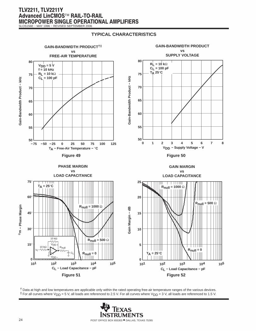
Figure 49
Gai
n-B
andw
idth
Pro
duct
− k
Hz
GAIN-BANDWIDTH PRODUCT †‡
vsFREE-AIR TEMPERATURE
TA − Free-Air Temperature − °C
70
55
50
75
80
−50 −25 0 25 50 10075
65
VDD = 5 Vf = 10 kHzRL = 10 kΩCL = 100 pF
125−75
60
Figure 50
GAIN-BANDWIDTH PRODUCTvs
SUPPLY VOLTAGE
VDD − Supply Voltage − V
Gai
n-B
andw
idth
Pro
duct
− k
Hz
65
55
50
75
80
1 2 3 4 5 76
60
RL = 10 kΩCL = 100 pFTA 25°C
80
70
Figure 51
om −
Pha
se M
argi
n
PHASE MARGINvs
LOAD CAPACITANCE
CL − Load Capacitance − pF
mφ
75°
60°
45°
30°
15°
0101 102 103 104 105
10 kΩ
10 kΩ
VDD −
VDD +Rnull
CLVI
+−
Rnull = 0
Rnull = 1000 Ω
Rnull = 500 Ω
TA = 25°C
Figure 52
Gai
n M
argi
n −
dB
GAIN MARGINvs
LOAD CAPACITANCE
CL − Load Capacitance − pF
25
20
15
10
5
0101 102 103 104 105
Rnull = 0
Rnull = 1000 Ω
Rnull = 500 Ω
TA = 25°C
† Data at high and low temperatures are applicable only within the rated operating free-air temperature ranges of the various devices.‡ For all curves where VDD = 5 V, all loads are referenced to 2.5 V. For all curves where VDD = 3 V, all loads are referenced to 1.5 V.
SLOS156E − MAY 1996 − REVISED SEPTEMBER 2006
25POST OFFICE BOX 655303 • DALLAS, TEXAS 75265
TYPICAL CHARACTERISTICS
− U
nity
-Gai
n B
andw
idth
− k
Hz
UNITY-GAIN BANDWIDTHvs
LOAD CAPACITANCE
CL − Load Capacitance − pF
ÁÁÁÁÁÁ
B1
60
10
40
0
80
50
70
20
30
101 102 103 104 105
TA = 25°C
106
Figure 53
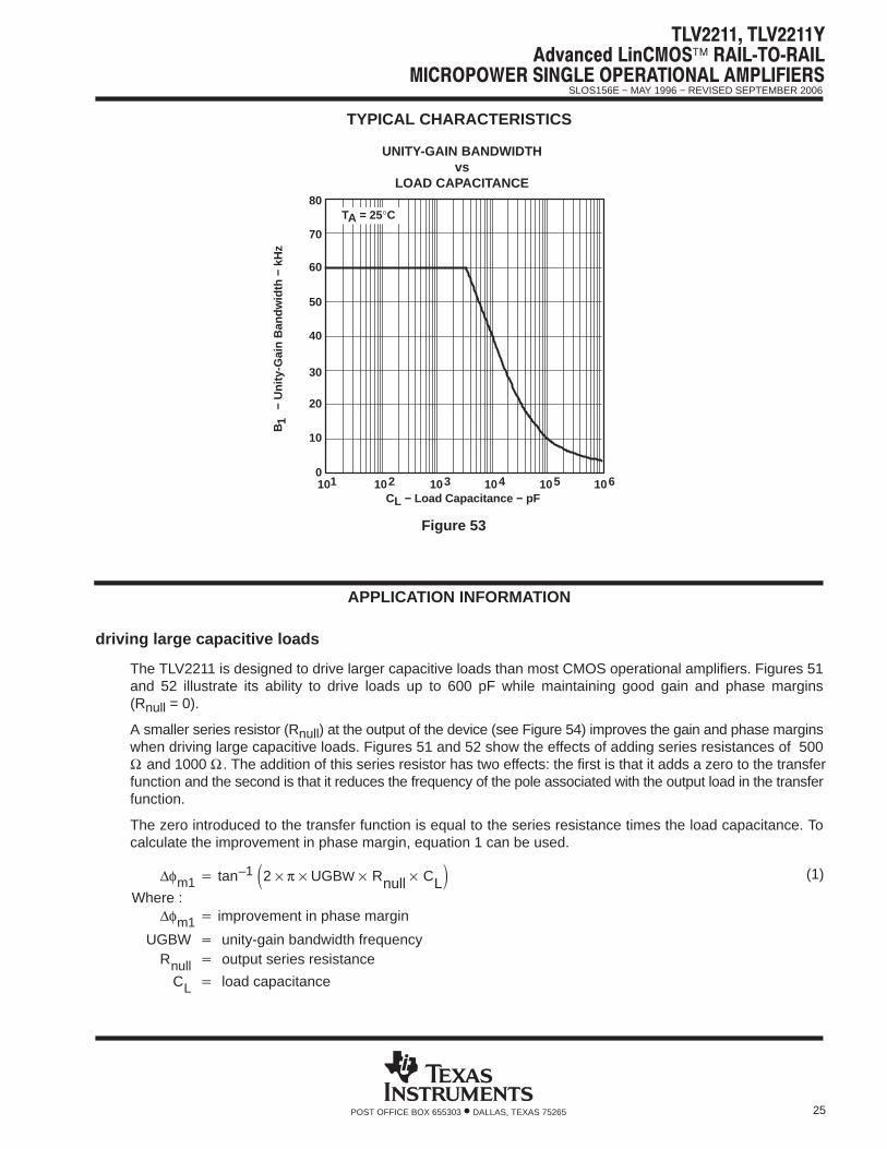
APPLICATION INFORMATION
driving large capacitive loads
The TLV2211 is designed to drive larger capacitive loads than most CMOS operational amplifiers. Figures 51and 52 illustrate its ability to drive loads up to 600 pF while maintaining good gain and phase margins(Rnull = 0).
A smaller series resistor (Rnull) at the output of the device (see Figure 54) improves the gain and phase marginswhen driving large capacitive loads. Figures 51 and 52 show the effects of adding series resistances of 500Ω and 1000 Ω . The addition of this series resistor has two effects: the first is that it adds a zero to the transferfunction and the second is that it reduces the frequency of the pole associated with the output load in the transferfunction.
The zero introduced to the transfer function is equal to the series resistance times the load capacitance. Tocalculate the improvement in phase margin, equation 1 can be used.
∆φm1 tan–1 2 × π × UGBW × Rnull × CL
∆φm1 improvement in phase margin
UGBW unity-gain bandwidth frequencyRnull output series resistance
CL load capacitance
(1)
Where :

SLOS156E − MAY 1996 − REVISED SEPTEMBER 2006
26 POST OFFICE BOX 655303 • DALLAS, TEXAS 75265
APPLICATION INFORMATION
driving large capacitive loads (continued)
The unity-gain bandwidth (UGBW) frequency decreases as the capacitive load increases (see Figure 54). Touse equation 1, UGBW must be approximated from Figure 54.
10 kΩ
10 kΩ
VDD−/GND
VDD+
Rnull
CL
VI
+
−
Figure 54. Series-Resistance Circuit
driving heavy dc loads
The TLV2211 is designed to provide better sinking and sourcing output currents than earlier CMOS rail-to-railoutput devices. This device is specified to sink 500 µA and source 250 µA at VDD = 3 V and VDD = 5 V at amaximum quiescent IDD of 25 µA. This provides a greater than 90% power efficiency.
When driving heavy dc loads, such as 10 kΩ, the positive edge can experience some distortion under slewingconditions. This condition can be seen in Figure 39. This condition is affected by three factors:
Where the load is referenced. When the load is referenced to either rail, this condition does not occur. Thedistortion occurs only when the output signal swings through the point where the load is referenced.Figure 40 illustrates two 10-kΩ load conditions. The first load condition shows the distortion seen for a10-kΩ load tied to 2.5 V. The third load condition shows no distortion for a 10-kΩ load tied to 0 V.
Load resistance. As the load resistance increases, the distortion seen on the output decreases. Figure 40illustrates the difference seen on the output for a 10-kΩ load and a 100-kΩ load with both tied to 2.5 V.
Input signal edge rate. Faster input edge rates for a step input result in more distortion than with slower inputedge rates.

SLOS156E − MAY 1996 − REVISED SEPTEMBER 2006
27POST OFFICE BOX 655303 • DALLAS, TEXAS 75265
APPLICATION INFORMATION
macromodel information
Macromodel information provided was derived using Microsim Parts, the model generation software usedwith Microsim PSpice. The Boyle macromodel (see Note 6) and subcircuit in Figure 54 are generated usingthe TLV2211 typical electrical and operating characteristics at TA = 25°C. Using this information, outputsimulations of the following key parameters can be generated to a tolerance of 20% (in most cases):
Maximum positive output voltage swing Maximum negative output voltage swing Slew rate Quiescent power dissipation Input bias current Open-loop voltage amplification
Unity-gain frequency Common-mode rejection ratio Phase margin DC output resistance AC output resistance Short-circuit output current limit
NOTE 6: G. R. Boyle, B. M. Cohn, D. O. Pederson, and J. E. Solomon, “Macromodeling of Integrated Circuit Operational Amplifiers”, IEEE Journalof Solid-State Circuits, SC-9, 353 (1974).
OUT
+
−
+
−
+
−
+
−
+−
+
−
+
− +
−
+−
.SUBCKT TLV2211 1 2 3 4 5C1 11 12 8.86E−12C2 6 7 50.00E−12DC 5 53 DXDE 54 5 DXDLP 90 91 DXDLN 92 90 DXDP 4 3 DXEGND 99 0 POLY (2) (3,0) (4,0) 0 .5 .5FB 7 99 POLY (5) VB VC VE VLP+ VLN 0 4.29E6 −6E6 6E6 6E6 −6E6GA 6 0 11 12 9.425E−6GCM 0 6 10 99 1320.2E−12ISS 3 10 DC 1.250E−6HLIM 90 0 VLIM 1KJ1 11 2 10 JXJ2 12 1 10 JXR2 6 9 100.0E3
RD1 60 11 106.1E3RD2 60 12 106.1E3R01 8 5 50R02 7 99 150RP 3 4 419.2E3RSS 10 99 160.0E6VAD 60 4 −.5VB 9 0 DC 0VC 3 53 DC .55VE 54 4 DC .55VLIM 7 8 DC 0VLP 91 0 DC 0.1VLN 0 92 DC 2.6.MODEL DX D (IS=800.0E−18).MODEL JX PJF (IS=500.0E−15 BETA=166E−6+ VTO=−.004).ENDS
VDD+
RP
IN −2
IN+1
VDD−
VAD
RD1
11
J1 J2
10
RSS ISS
3
12
RD2
60
VE
54DE
DP
VC
DC
4
C1
53
R2
6
9
EGND
VB
FB
C2
GCM GA VLIM
8
5
RO1
RO2
HLIM
90
DLP
91
DLN
92
VLNVLP
99
7
Figure 55. Boyle Macromodel and Subcircuit
PSpice and Parts are trademark of MicroSim Corporation.
"!#!)% %#&)$! #!)% !" !$+" #!)% '"! (. " $). !" " $). " !$ -""$ (. % &)). "'"%$/ ))! $+ %' $! !'"$/ +" $"%$ % ! $+%# !& $!" '"!& $ $! -+ + $+ #!) ")$%*
TAPE AND REEL INFORMATION
*All dimensions are nominal
Device PackageType
PackageDrawing
Pins SPQ ReelDiameter
(mm)
ReelWidth
W1 (mm)
A0(mm)
B0(mm)
K0(mm)
P1(mm)
W(mm)
Pin1Quadrant
TLV2211CDBVR SOT-23 DBV 5 3000 180.0 9.0 3.15 3.2 1.4 4.0 8.0 Q3
TLV2211CDBVT SOT-23 DBV 5 250 180.0 9.0 3.15 3.2 1.4 4.0 8.0 Q3
TLV2211IDBVR SOT-23 DBV 5 3000 178.0 9.0 3.3 3.2 1.4 4.0 8.0 Q3
TLV2211IDBVR SOT-23 DBV 5 3000 180.0 9.0 3.15 3.2 1.4 4.0 8.0 Q3
TLV2211IDBVT SOT-23 DBV 5 250 180.0 9.0 3.15 3.2 1.4 4.0 8.0 Q3
PACKAGE MATERIALS INFORMATION
www.ti.com 21-Apr-2017
Pack Materials-Page 1
*All dimensions are nominal
Device Package Type Package Drawing Pins SPQ Length (mm) Width (mm) Height (mm)
TLV2211CDBVR SOT-23 DBV 5 3000 182.0 182.0 20.0
TLV2211CDBVT SOT-23 DBV 5 250 182.0 182.0 20.0
TLV2211IDBVR SOT-23 DBV 5 3000 180.0 180.0 18.0
TLV2211IDBVR SOT-23 DBV 5 3000 182.0 182.0 20.0
TLV2211IDBVT SOT-23 DBV 5 250 182.0 182.0 20.0
PACKAGE MATERIALS INFORMATION
www.ti.com 21-Apr-2017
Pack Materials-Page 2


www.ti.com
PACKAGE OUTLINE
C
TYP0.220.08
0.25
3.02.6
2X 0.95
1.9
1.45 MAX
TYP0.150.00
5X 0.50.3
TYP0.60.3
TYP80
1.9
A
3.052.75
B1.751.45
(1.1)
SOT-23 - 1.45 mm max heightDBV0005ASMALL OUTLINE TRANSISTOR
4214839/C 04/2017
NOTES: 1. All linear dimensions are in millimeters. Any dimensions in parenthesis are for reference only. Dimensioning and tolerancing per ASME Y14.5M.2. This drawing is subject to change without notice.3. Refernce JEDEC MO-178.
0.2 C A B
1
34
5
2
INDEX AREAPIN 1
GAGE PLANE
SEATING PLANE
0.1 C
SCALE 4.000
www.ti.com
EXAMPLE BOARD LAYOUT
0.07 MAXARROUND
0.07 MINARROUND
5X (1.1)
5X (0.6)
(2.6)
(1.9)
2X (0.95)
(R0.05) TYP
4214839/C 04/2017
SOT-23 - 1.45 mm max heightDBV0005ASMALL OUTLINE TRANSISTOR
NOTES: (continued) 4. Publication IPC-7351 may have alternate designs. 5. Solder mask tolerances between and around signal pads can vary based on board fabrication site.
SYMM
LAND PATTERN EXAMPLEEXPOSED METAL SHOWN
SCALE:15X
PKG
1
3 4
5
2
SOLDER MASKOPENINGMETAL UNDER
SOLDER MASK
SOLDER MASKDEFINED
EXPOSED METAL
METALSOLDER MASKOPENING
NON SOLDER MASKDEFINED
(PREFERRED)
SOLDER MASK DETAILS
EXPOSED METAL
www.ti.com
EXAMPLE STENCIL DESIGN
(2.6)
(1.9)
2X(0.95)
5X (1.1)
5X (0.6)
(R0.05) TYP
SOT-23 - 1.45 mm max heightDBV0005ASMALL OUTLINE TRANSISTOR
4214839/C 04/2017
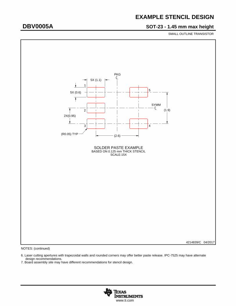
NOTES: (continued) 6. Laser cutting apertures with trapezoidal walls and rounded corners may offer better paste release. IPC-7525 may have alternate design recommendations. 7. Board assembly site may have different recommendations for stencil design.
SOLDER PASTE EXAMPLEBASED ON 0.125 mm THICK STENCIL
SCALE:15X
SYMM
PKG
1
3 4
5
2
IMPORTANT NOTICE
Texas Instruments Incorporated (TI) reserves the right to make corrections, enhancements, improvements and other changes to itssemiconductor products and services per JESD46, latest issue, and to discontinue any product or service per JESD48, latest issue. Buyersshould obtain the latest relevant information before placing orders and should verify that such information is current and complete.TI’s published terms of sale for semiconductor products (http://www.ti.com/sc/docs/stdterms.htm) apply to the sale of packaged integratedcircuit products that TI has qualified and released to market. Additional terms may apply to the use or sale of other types of TI products andservices.Reproduction of significant portions of TI information in TI data sheets is permissible only if reproduction is without alteration and isaccompanied by all associated warranties, conditions, limitations, and notices. TI is not responsible or liable for such reproduceddocumentation. Information of third parties may be subject to additional restrictions. Resale of TI products or services with statementsdifferent from or beyond the parameters stated by TI for that product or service voids all express and any implied warranties for theassociated TI product or service and is an unfair and deceptive business practice. TI is not responsible or liable for any such statements.Buyers and others who are developing systems that incorporate TI products (collectively, “Designers”) understand and agree that Designersremain responsible for using their independent analysis, evaluation and judgment in designing their applications and that Designers havefull and exclusive responsibility to assure the safety of Designers' applications and compliance of their applications (and of all TI productsused in or for Designers’ applications) with all applicable regulations, laws and other applicable requirements. Designer represents that, withrespect to their applications, Designer has all the necessary expertise to create and implement safeguards that (1) anticipate dangerousconsequences of failures, (2) monitor failures and their consequences, and (3) lessen the likelihood of failures that might cause harm andtake appropriate actions. Designer agrees that prior to using or distributing any applications that include TI products, Designer willthoroughly test such applications and the functionality of such TI products as used in such applications.TI’s provision of technical, application or other design advice, quality characterization, reliability data or other services or information,including, but not limited to, reference designs and materials relating to evaluation modules, (collectively, “TI Resources”) are intended toassist designers who are developing applications that incorporate TI products; by downloading, accessing or using TI Resources in anyway, Designer (individually or, if Designer is acting on behalf of a company, Designer’s company) agrees to use any particular TI Resourcesolely for this purpose and subject to the terms of this Notice.TI’s provision of TI Resources does not expand or otherwise alter TI’s applicable published warranties or warranty disclaimers for TIproducts, and no additional obligations or liabilities arise from TI providing such TI Resources. TI reserves the right to make corrections,enhancements, improvements and other changes to its TI Resources. TI has not conducted any testing other than that specificallydescribed in the published documentation for a particular TI Resource.Designer is authorized to use, copy and modify any individual TI Resource only in connection with the development of applications thatinclude the TI product(s) identified in such TI Resource. NO OTHER LICENSE, EXPRESS OR IMPLIED, BY ESTOPPEL OR OTHERWISETO ANY OTHER TI INTELLECTUAL PROPERTY RIGHT, AND NO LICENSE TO ANY TECHNOLOGY OR INTELLECTUAL PROPERTYRIGHT OF TI OR ANY THIRD PARTY IS GRANTED HEREIN, including but not limited to any patent right, copyright, mask work right, orother intellectual property right relating to any combination, machine, or process in which TI products or services are used. Informationregarding or referencing third-party products or services does not constitute a license to use such products or services, or a warranty orendorsement thereof. Use of TI Resources may require a license from a third party under the patents or other intellectual property of thethird party, or a license from TI under the patents or other intellectual property of TI.TI RESOURCES ARE PROVIDED “AS IS” AND WITH ALL FAULTS. TI DISCLAIMS ALL OTHER WARRANTIES ORREPRESENTATIONS, EXPRESS OR IMPLIED, REGARDING RESOURCES OR USE THEREOF, INCLUDING BUT NOT LIMITED TOACCURACY OR COMPLETENESS, TITLE, ANY EPIDEMIC FAILURE WARRANTY AND ANY IMPLIED WARRANTIES OFMERCHANTABILITY, FITNESS FOR A PARTICULAR PURPOSE, AND NON-INFRINGEMENT OF ANY THIRD PARTY INTELLECTUALPROPERTY RIGHTS. TI SHALL NOT BE LIABLE FOR AND SHALL NOT DEFEND OR INDEMNIFY DESIGNER AGAINST ANY CLAIM,INCLUDING BUT NOT LIMITED TO ANY INFRINGEMENT CLAIM THAT RELATES TO OR IS BASED ON ANY COMBINATION OFPRODUCTS EVEN IF DESCRIBED IN TI RESOURCES OR OTHERWISE. IN NO EVENT SHALL TI BE LIABLE FOR ANY ACTUAL,DIRECT, SPECIAL, COLLATERAL, INDIRECT, PUNITIVE, INCIDENTAL, CONSEQUENTIAL OR EXEMPLARY DAMAGES INCONNECTION WITH OR ARISING OUT OF TI RESOURCES OR USE THEREOF, AND REGARDLESS OF WHETHER TI HAS BEENADVISED OF THE POSSIBILITY OF SUCH DAMAGES.Unless TI has explicitly designated an individual product as meeting the requirements of a particular industry standard (e.g., ISO/TS 16949and ISO 26262), TI is not responsible for any failure to meet such industry standard requirements.Where TI specifically promotes products as facilitating functional safety or as compliant with industry functional safety standards, suchproducts are intended to help enable customers to design and create their own applications that meet applicable functional safety standardsand requirements. Using products in an application does not by itself establish any safety features in the application. Designers mustensure compliance with safety-related requirements and standards applicable to their applications. Designer may not use any TI products inlife-critical medical equipment unless authorized officers of the parties have executed a special contract specifically governing such use.Life-critical medical equipment is medical equipment where failure of such equipment would cause serious bodily injury or death (e.g., lifesupport, pacemakers, defibrillators, heart pumps, neurostimulators, and implantables). Such equipment includes, without limitation, allmedical devices identified by the U.S. Food and Drug Administration as Class III devices and equivalent classifications outside the U.S.TI may expressly designate certain products as completing a particular qualification (e.g., Q100, Military Grade, or Enhanced Product).Designers agree that it has the necessary expertise to select the product with the appropriate qualification designation for their applicationsand that proper product selection is at Designers’ own risk. Designers are solely responsible for compliance with all legal and regulatoryrequirements in connection with such selection.Designer will fully indemnify TI and its representatives against any damages, costs, losses, and/or liabilities arising out of Designer’s non-compliance with the terms and provisions of this Notice.
Mailing Address: Texas Instruments, Post Office Box 655303, Dallas, Texas 75265Copyright © 2018, Texas Instruments Incorporated