Embed Size (px)
Citation preview
PCB(Printed Circuit Board)
Presented
By
S.Muthumari
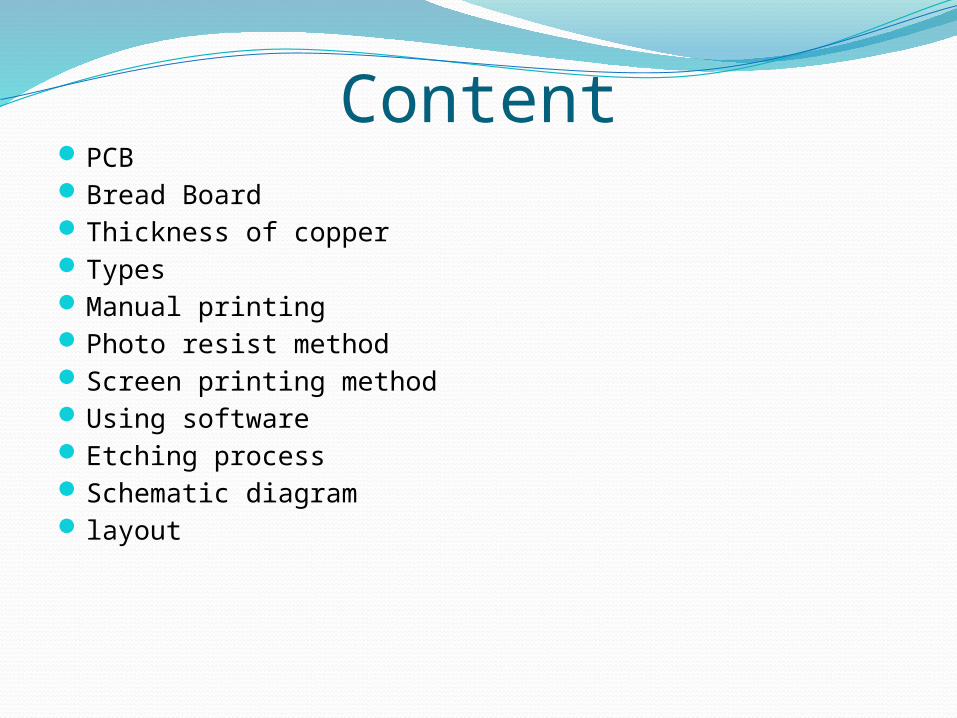
ContentPCBBread BoardThickness of copperTypes Manual printingPhoto resist methodScreen printing methodUsing software Etching processSchematic diagram layout
Difference between PCB Layout and bread board connection
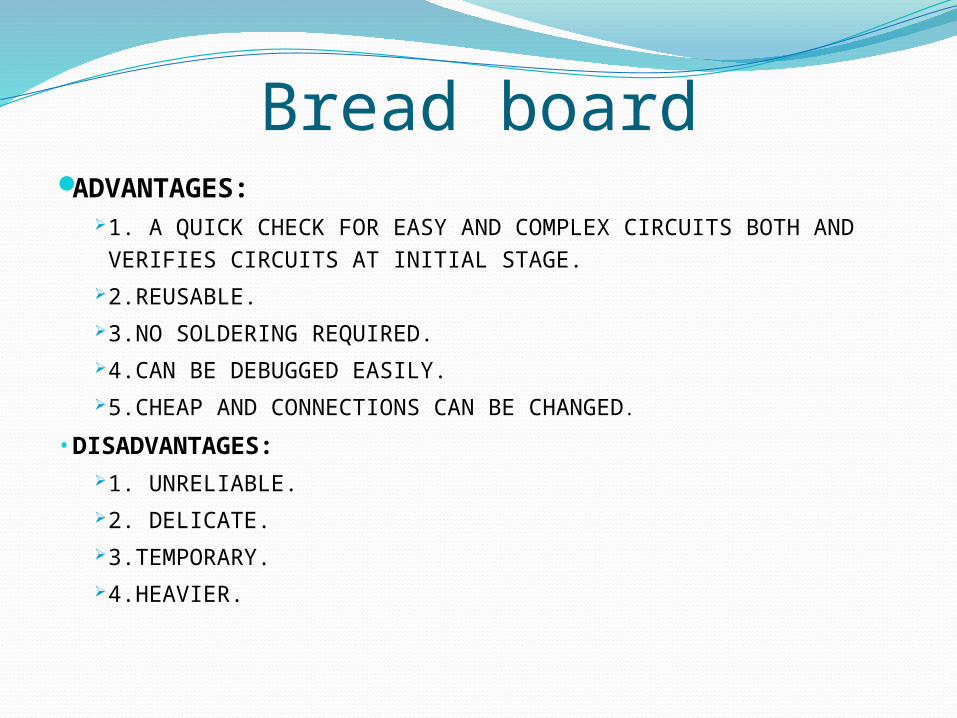
Bread boardADVANTAGES:
1. A QUICK CHECK FOR EASY AND COMPLEX CIRCUITS BOTH AND
VERIFIES CIRCUITS AT INITIAL STAGE.
2.REUSABLE.
3.NO SOLDERING REQUIRED.
4.CAN BE DEBUGGED EASILY.
5.CHEAP AND CONNECTIONS CAN BE CHANGED.
• DISADVANTAGES: 1. UNRELIABLE.
2. DELICATE.
3.TEMPORARY.
4.HEAVIER.
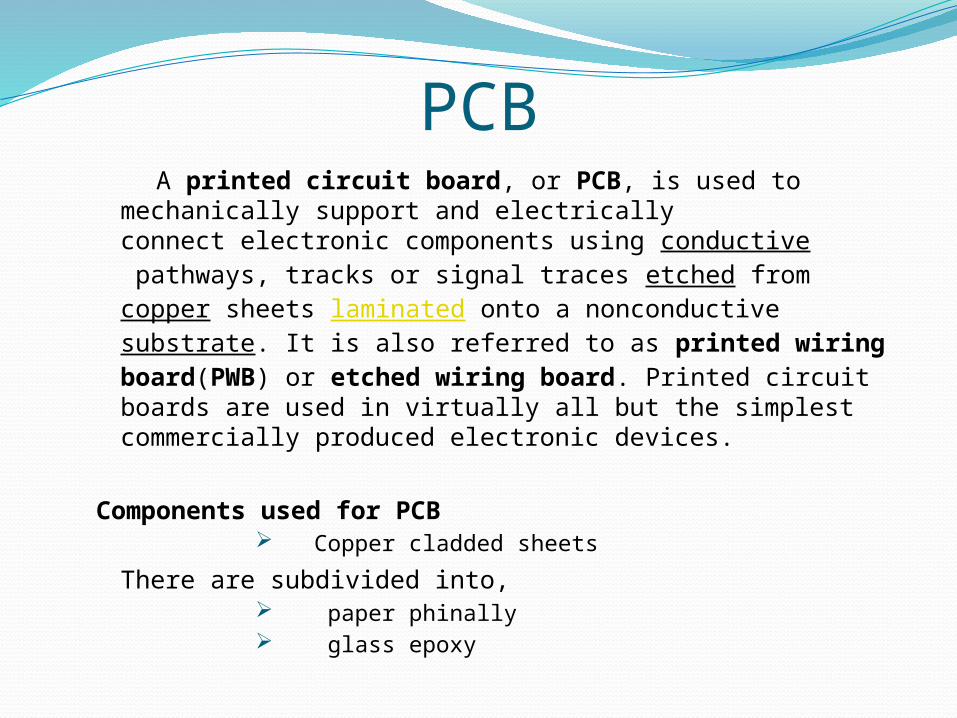
PCB A printed circuit board, or PCB, is used to mechanically support and
electrically connect electronic components using conductive pathways, tracks or signal traces etched from copper sheets laminated onto a nonconductive substrate. It is also referred to as printed wiring board(PWB) or etched wiring board. Printed circuit boards are used in virtually all but the simplest commercially produced electronic devices.
Components used for PCB Copper cladded sheets
There are subdivided into, paper phinally glass epoxy
Advantages of PCB Inexpensive/cheaper
High volume production
Automated soldering is possible
Highly reliable
Hold the component easily
Thickness Of Copper
0.8mm(used for low power component( e.g.: slim phone,smd,multimeter)
1.6mm(used in commercial purpose)
3.2mm(power electronics side
Examples: MOSFET, Diode.
Types Manual printing.
Photo resist method.
Screen printing
Using software
Manual printing• Get the required size copper board.
• Draw the layout on the board using permanent marker or nail police.
• Etching process.
• Fix the component on the board
• Check the output
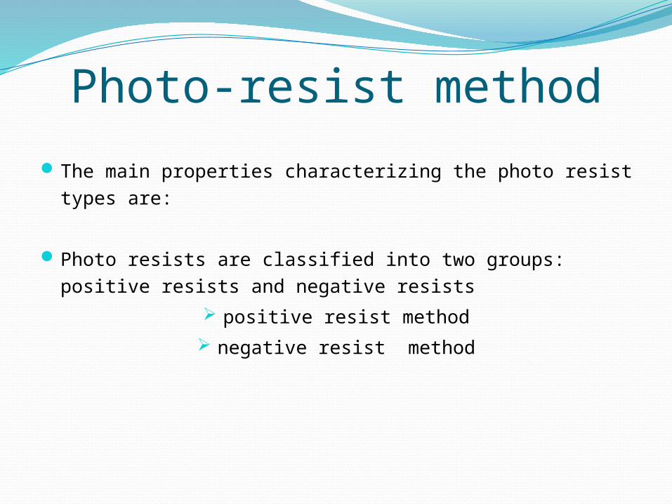
Photo-resist method
The main properties characterizing the photo resist types are:
Photo resists are classified into two groups: positive resists and negative
resists
positive resist method
negative resist method
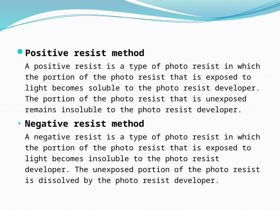
Positive resist method
A positive resist is a type of photo resist in which the
portion of the photo resist that is exposed to light becomes soluble to the
photo resist developer. The portion of the photo resist that is unexposed
remains insoluble to the photo resist developer.
• Negative resist method
A negative resist is a type of photo resist in which the
portion of the photo resist that is exposed to light becomes insoluble to the
photo resist developer. The unexposed portion of the photo resist is
dissolved by the photo resist developer.
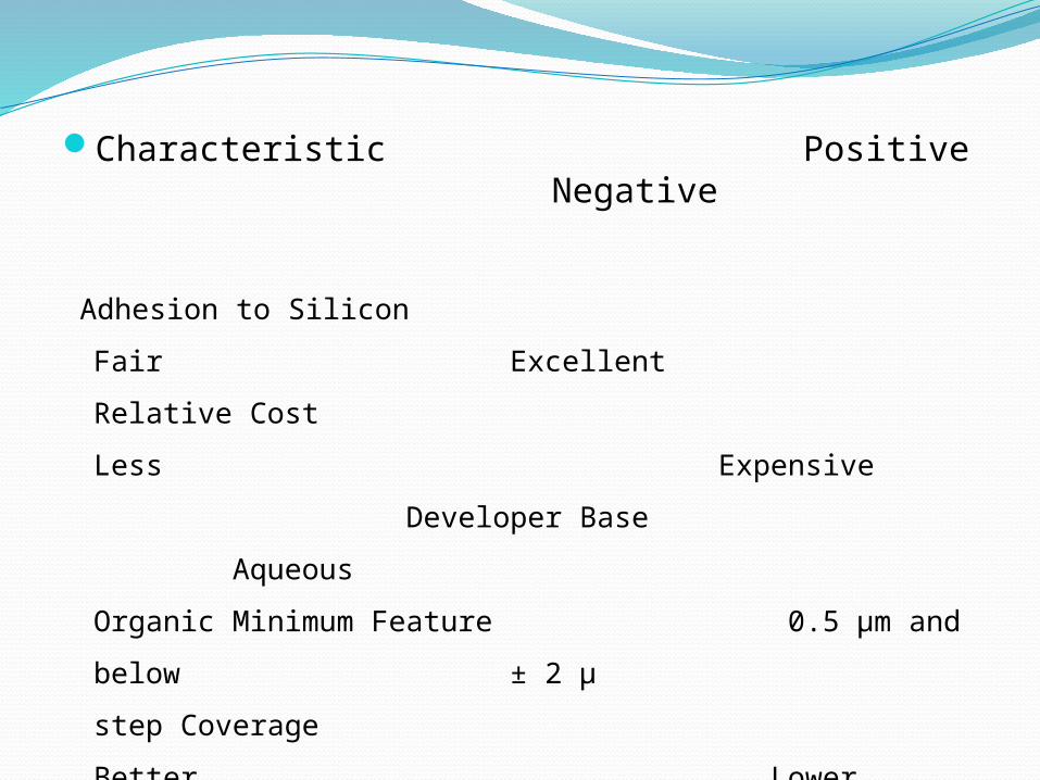
Characteristic Positive Negative
Adhesion to Silicon Fair Excellent
Relative Cost Less
Expensive Developer Base Aqueous
Organic Minimum Feature 0.5 μm and below
± 2 μ step Coverage Better
Lower
Wet Chemical Resistance Fair Excellent
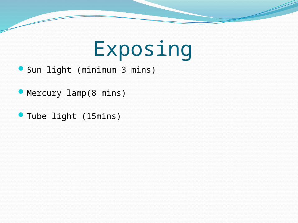
Exposing Sun light (minimum 3 mins)
Mercury lamp(8 mins)
Tube light (15mins)
Screen printing • Screen printing printed circuit boards is typically
performed in a clean, dust free room using semi-automatic
or fully-automatic screen printing presses. The most
common PCB panel size is 53 x 72 cm, with the printing
area around 50 x 70 cm. The printed panel may contain
many PCB panels that are printed at once, and will
eventually be separated.
1.4 Soldering Methods1.4.1. Hand soldering:
It is the oldest method of soldering, it is still popular method in certain kinds of applications: Development of prototype boards
Low volume production Soldering of extremely temperature sensitive components Solder reflow of fine pitch components using hot bar Rework or repair of machine soldered boards The main disadvantages are operator training, speed, and consistent
quality.
1.4.2 Machine Soldering:Two prominently used machine soldering types are:A. Wave Soldering
Primarily used for soldering through-hole components on to PCBs.
B. Reflow Soldering.
Used for soldering SMD components on to PCBs. Reflow soldering of SM components have the following advantages over manual soldering:
• Mass soldering• Consistency in manufacture through precise control of process
parameters.• flexible for small production runs as well.
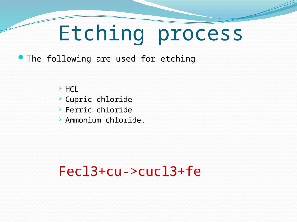
Etching processThe following are used for etching
HCL Cupric chloride Ferric chloride Ammonium chloride.
Fecl3+cu->cucl3+fe
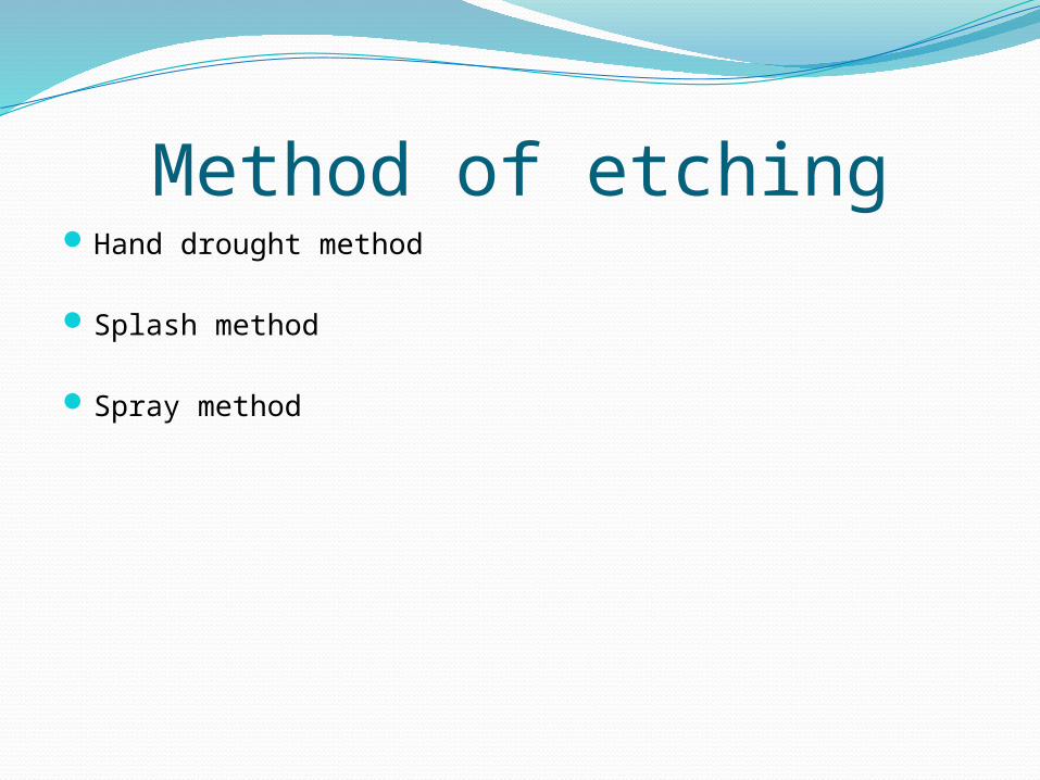
Method of etchingHand drought method
Splash method
Spray method
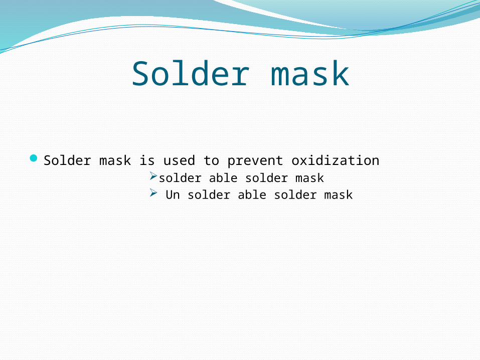
Solder mask
Solder mask is used to prevent oxidization solder able solder mask Un solder able solder mask
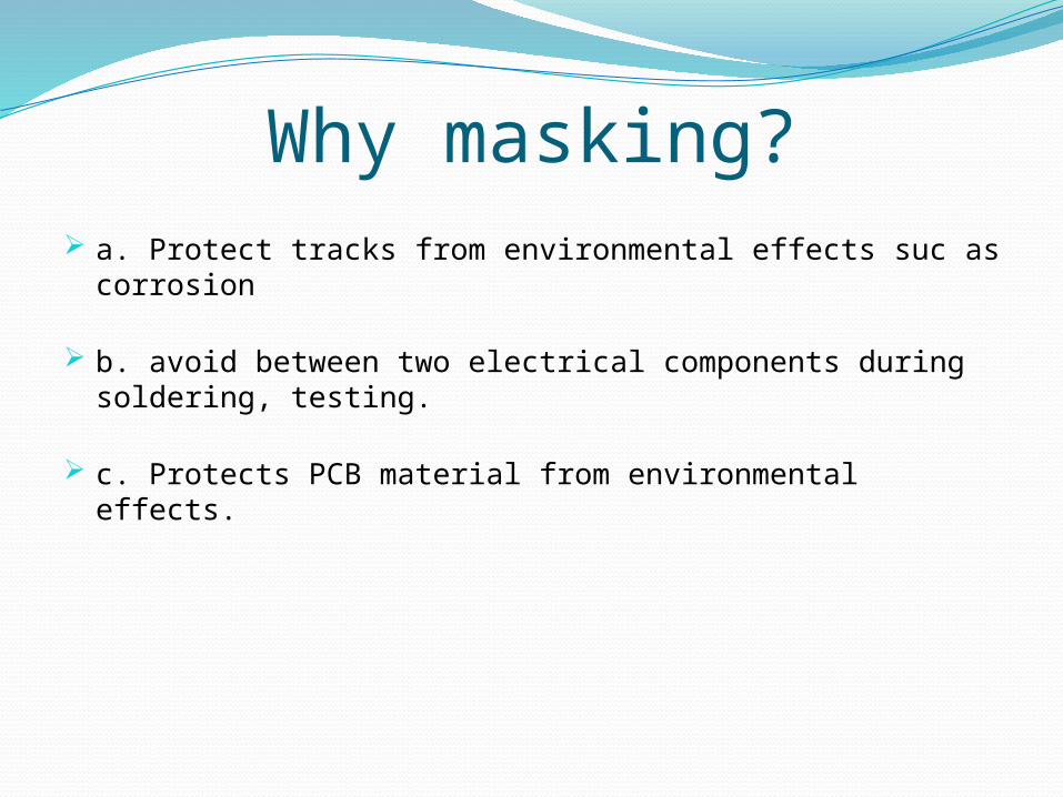
Why masking? a. Protect tracks from environmental effects suc as corrosion
b. avoid between two electrical components during soldering, testing.
c. Protects PCB material from environmental effects.
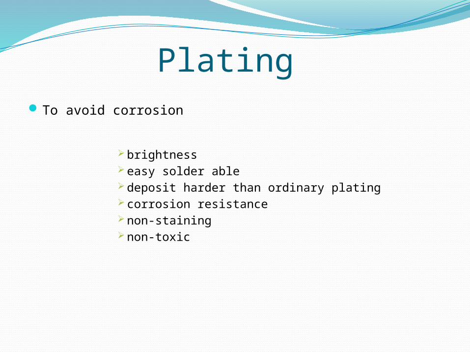
Plating To avoid corrosion
brightness easy solder able deposit harder than ordinary plating corrosion resistance non-staining non-toxic
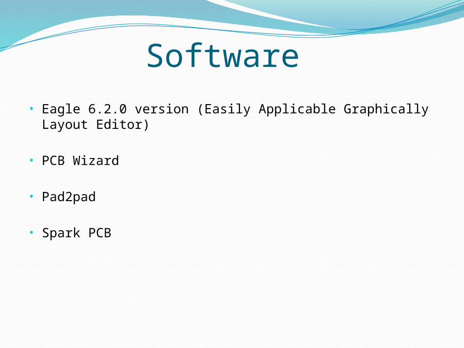
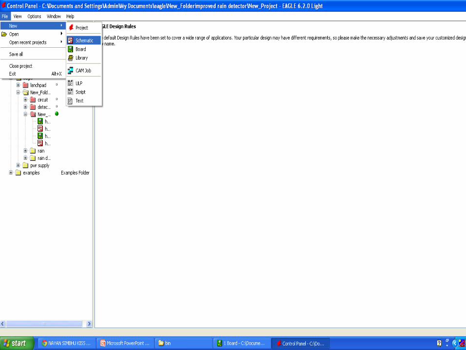
Software • Eagle 6.2.0 version (Easily Applicable Graphically Layout Editor)
• PCB Wizard
• Pad2pad
• Spark PCB
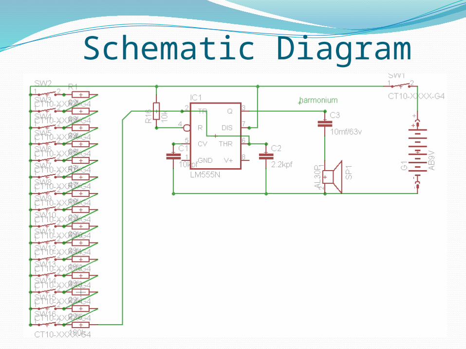
Schematic Diagram
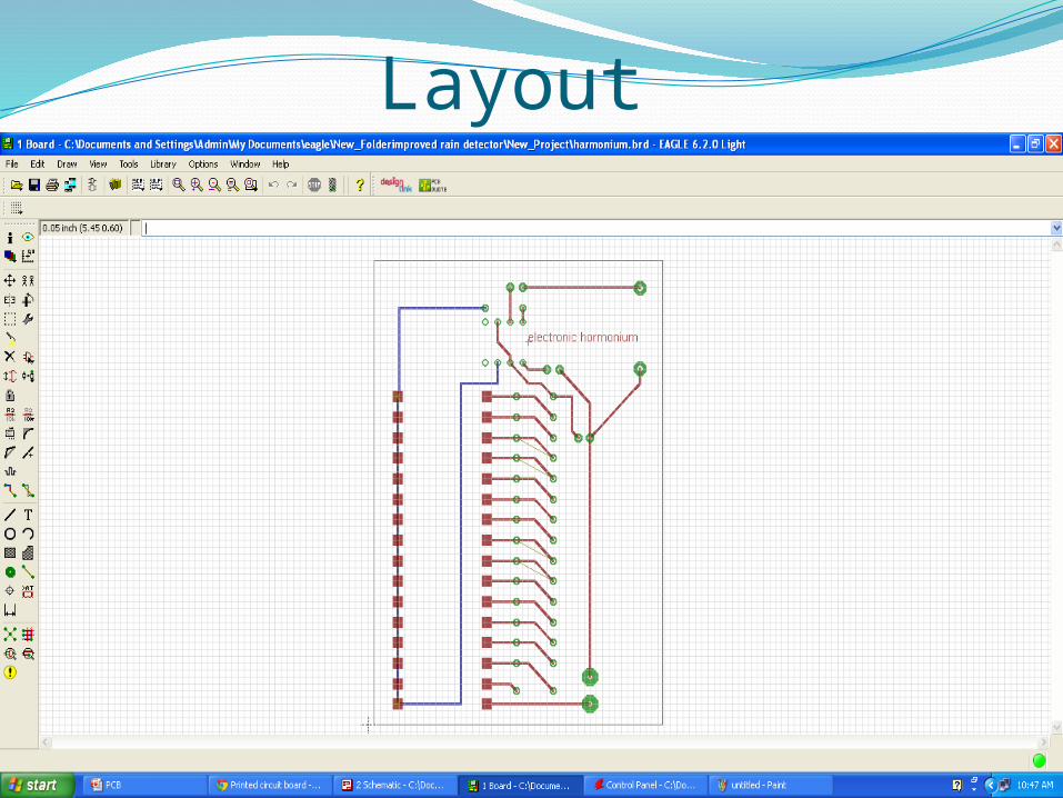
Layout
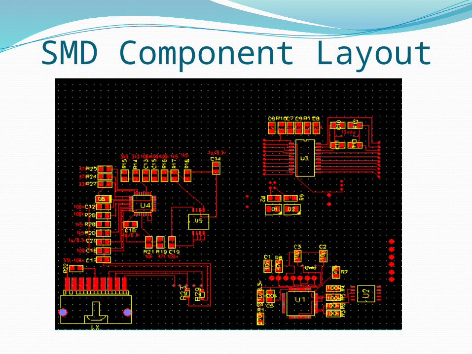
SMD Component Layout
THANK YOU?