Embed Size (px)
DESCRIPTION
3
Citation preview

Attia, John Okyere. “Operational Amplifiers.”Electronics and Circuit Analysis using MATLAB.Ed. John Okyere AttiaBoca Raton: CRC Press LLC, 1999
© 1999 by CRC PRESS LLC
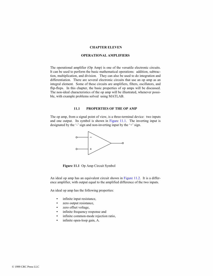
CHAPTER ELEVEN
OPERATIONAL AMPLIFIERS The operational amplifier (Op Amp) is one of the versatile electronic circuits. It can be used to perform the basic mathematical operations: addition, subtrac-tion, multiplication, and division. They can also be used to do integration and differentiation. There are several electronic circuits that use an op amp as an integral element. Some of these circuits are amplifiers, filters, oscillators, and flip-flops. In this chapter, the basic properties of op amps will be discussed. The non-ideal characteristics of the op amp will be illustrated, whenever possi-ble, with example problems solved using MATLAB.
11.1 PROPERTIES OF THE OP AMP The op amp, from a signal point of view, is a three-terminal device: two inputs and one output. Its symbol is shown in Figure 11.1. The inverting input is designated by the ‘-’ sign and non-inverting input by the ‘+’ sign.
Figure 11.1 Op Amp Circuit Symbol An ideal op amp has an equivalent circuit shown in Figure 11.2. It is a differ-ence amplifier, with output equal to the amplified difference of the two inputs. An ideal op amp has the following properties:
• infinite input resistance, • zero output resistance, • zero offset voltage, • infinite frequency response and • infinite common-mode rejection ratio, • infinite open-loop gain, A.
© 1999 CRC Press LLC
© 1999 CRC Press LLC
V1
V2- A(V2 - V1)
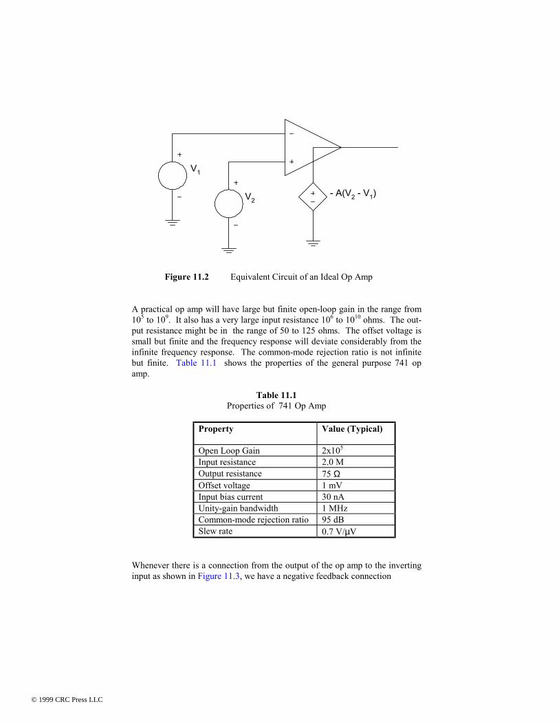
Figure 11.2 Equivalent Circuit of an Ideal Op Amp A practical op amp will have large but finite open-loop gain in the range from 105 to 109. It also has a very large input resistance 106 to 1010 ohms. The out-put resistance might be in the range of 50 to 125 ohms. The offset voltage is small but finite and the frequency response will deviate considerably from the infinite frequency response. The common-mode rejection ratio is not infinite but finite. Table 11.1 shows the properties of the general purpose 741 op amp.
Table 11.1 Properties of 741 Op Amp
Property
Value (Typical)
Open Loop Gain 2x10⁵ Input resistance 2.0 M Output resistance 75 Ω Offset voltage 1 mV Input bias current 30 nA Unity-gain bandwidth 1 MHz Common-mode rejection ratio 95 dB Slew rate 0.7 V/µV
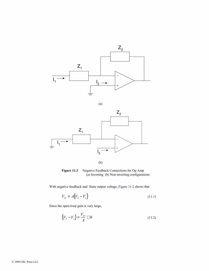
Whenever there is a connection from the output of the op amp to the inverting input as shown in Figure 11.3, we have a negative feedback connection
© 1999 CRC Press LLC
© 1999 CRC Press LLC
Z2
Z1
I2I1
(a)
Z2
Z1
I2
I1
(b) Figure 11.3 Negative Feedback Connections for Op Amp (a) Inverting (b) Non-inverting configurations With negative feedback and finite output voltage, Figure 11.2 shows that
( )V A V VO = −2 1 (11.1) Since the open-loop gain is very large,
( )V VVAO
2 1 0− = ≅ (11.2)
© 1999 CRC Press LLC
© 1999 CRC Press LLC
Equation (11.2) implies that the two input voltages are also equal. This condi-tion is termed the concept of the virtual short circuit. In addition, because of the large input resistance of the op amp, the latter is assumed to take no cur-rent for most calculations.
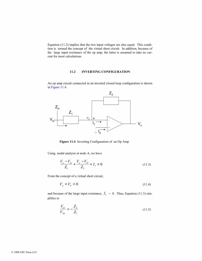
11.2 INVERTING CONFIGURATION An op amp circuit connected in an inverted closed loop configuration is shown in Figure 11.4.
I1
I2
Z1
Z2
Vo
Vin
Zin
Va A
Figure 11.4 Inverting Configuration of an Op Amp Using nodal analysis at node A, we have
V V
ZV V
ZIa in a O−
+−
+ =1 2
1 0 (11.3)
From the concept of a virtual short circuit,
V Va b= = 0 (11.4)
and because of the large input resistance, I1 = 0. Thus, Equation (11.3) sim-plifies to
VV
ZZ
O
IN= − 2
1 (11.5)
© 1999 CRC Press LLC
© 1999 CRC Press LLC
The minus sign implies that VIN and V0 are out of phase by 180o. The input impedance, ZIN , is given as
ZVI
ZININ= =1
1 (11.6)
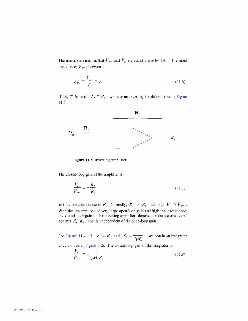
If Z R1 1= and Z R2 2= , we have an inverting amplifier shown in Figure 11.5.
Vo
Vin
R2
R1
Figure 11.5 Inverting Amplifier The closed-loop gain of the amplifier is
VV
RR
O
IN= − 2
1 (11.7)
and the input resistance is R1 . Normally, R2 > R1 such that V VIN0 > . With the assumptions of very large open-loop gain and high input resistance, the closed-loop gain of the inverting amplifier depends on the external com-ponents R1 , R2 , and is independent of the open-loop gain.
For Figure 11.4, if Z R1 1= and ZjwC21
= , we obtain an integrator
circuit shown in Figure 11.6. The closed-loop gain of the integrator is
VV jwCR
O
IN= −
1
1 (11.8)
© 1999 CRC Press LLC
© 1999 CRC Press LLC
Vo
Vin
C
R1
IC
IR
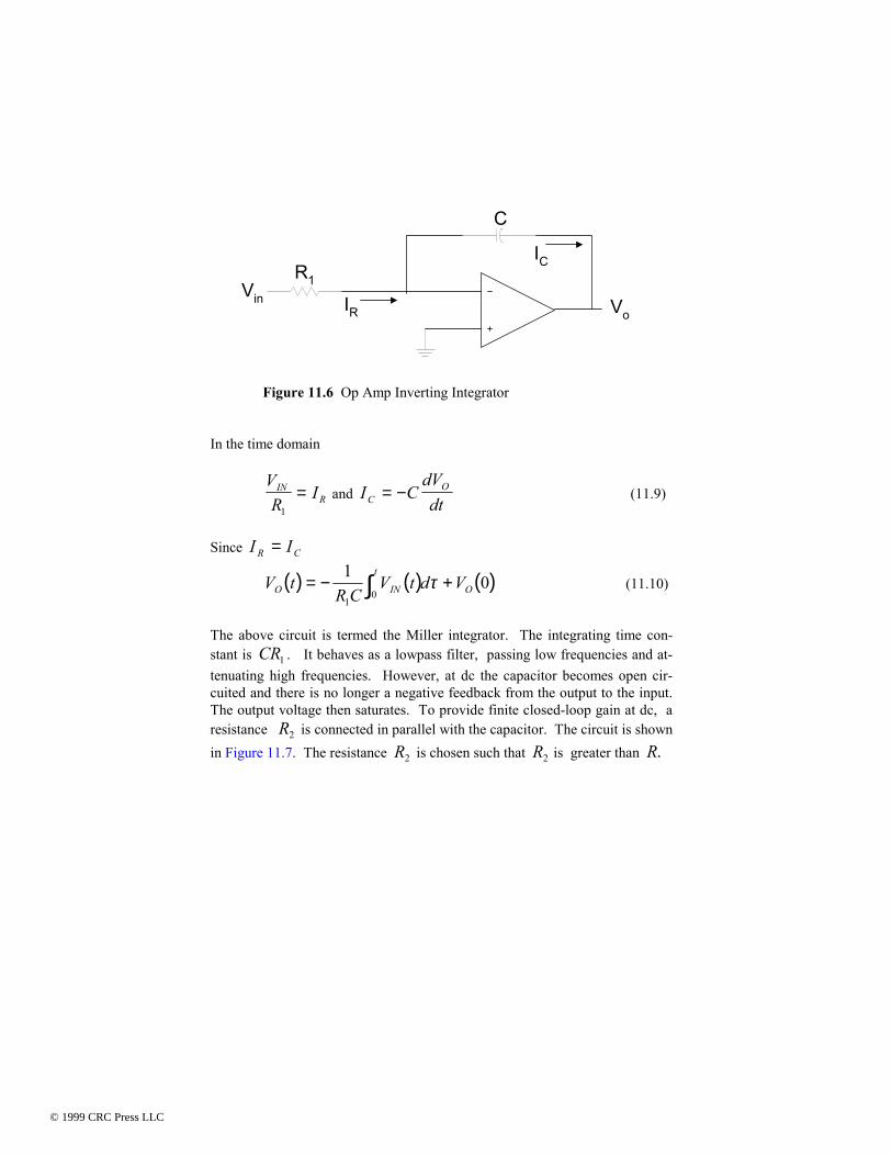
Figure 11.6 Op Amp Inverting Integrator In the time domain
VR
IINR
1= and I C
dVdtC
O= − (11.9)
Since I IR C=
( ) ( ) ( )V tR C
V t d VO IN
t
O= − +∫1
01
0τ (11.10)
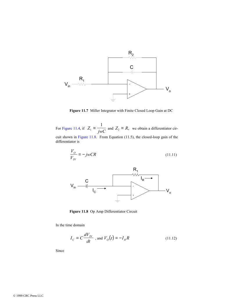
The above circuit is termed the Miller integrator. The integrating time con-stant is CR1 . It behaves as a lowpass filter, passing low frequencies and at-tenuating high frequencies. However, at dc the capacitor becomes open cir-cuited and there is no longer a negative feedback from the output to the input. The output voltage then saturates. To provide finite closed-loop gain at dc, a resistance R2 is connected in parallel with the capacitor. The circuit is shown in Figure 11.7. The resistance R2 is chosen such that R2 is greater than R.
© 1999 CRC Press LLC
© 1999 CRC Press LLC
Vo
Vin
C
R1
R2
Figure 11.7 Miller Integrator with Finite Closed Loop Gain at DC
For Figure 11.4, if ZjwC1
1= and Z R2 = , we obtain a differentiator cir-
cuit shown in Figure 11.8. From Equation (11.5), the closed-loop gain of the differentiator is
VV
jwCRO
IN= − (11.11)
Vo
Vin
C
R1
IR
IC
Figure 11.8 Op Amp Differentiator Circuit In the time domain
I CdV
dtCIN= , and ( )V t I RO R= − (11.12)
Since
© 1999 CRC Press LLC
© 1999 CRC Press LLC
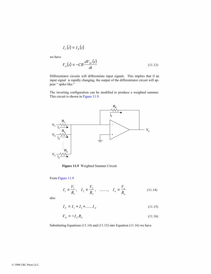
( ) ( )I t I tC R= we have
( )( )
V t CRdV t
dtOIN= − (11.13)
Differentiator circuits will differentiate input signals. This implies that if an input signal is rapidly changing, the output of the differentiator circuit will ap-pear “ spike-like.” The inverting configuration can be modified to produce a weighted summer. This circuit is shown in Figure 11.9.
R1
R2
RF
Rn
In
IF
V1
V2
Vn
I1
I2
Vo
Figure 11.9 Weighted Summer Circuit
From Figure 11.9
IVR
IVR
IVRn
n
n1
1
12
2
2= = =, , ......., (11.14)
also I I I IF N= + +1 2 ...... (11.15) V I RO F F= − (11.16)
Substituting Equations (11.14) and (11.15) into Equation (11.16) we have
© 1999 CRC Press LLC
© 1999 CRC Press LLC
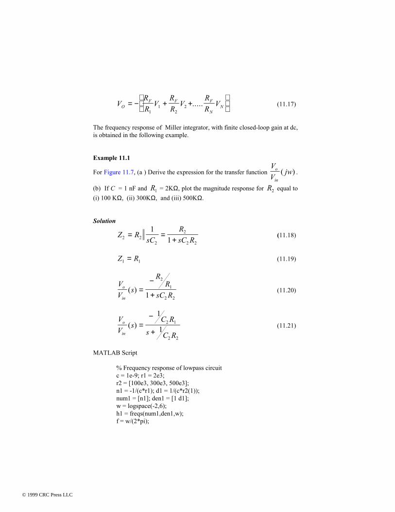
VRR
VRR
VRR
VOF F F
NN= − + +
11
22 ..... (11.17)
The frequency response of Miller integrator, with finite closed-loop gain at dc, is obtained in the following example. Example 11.1
For Figure 11.7, (a ) Derive the expression for the transfer function VV
jwo
in( ) .
(b) If C = 1 nF and R1 = 2KΩ, plot the magnitude response for R2 equal to (i) 100 KΩ, (ii) 300KΩ, and (iii) 500KΩ. Solution
Z RsC
RsC R2 2
2
2
2 2
11
= =+
(11.18)
Z R1 1= (11.19)
VV
s
RR
sC Ro
in( ) =
−
+
2
1
2 21 (11.20)
VV
sC R
s C R
o
in( ) =
−
+
1
12 1
2 2
(11.21)
MATLAB Script
% Frequency response of lowpass circuit c = 1e-9; r1 = 2e3; r2 = [100e3, 300e3, 500e3]; n1 = -1/(c*r1); d1 = 1/(c*r2(1)); num1 = [n1]; den1 = [1 d1]; w = logspace(-2,6); h1 = freqs(num1,den1,w); f = w/(2*pi);
© 1999 CRC Press LLC
© 1999 CRC Press LLC
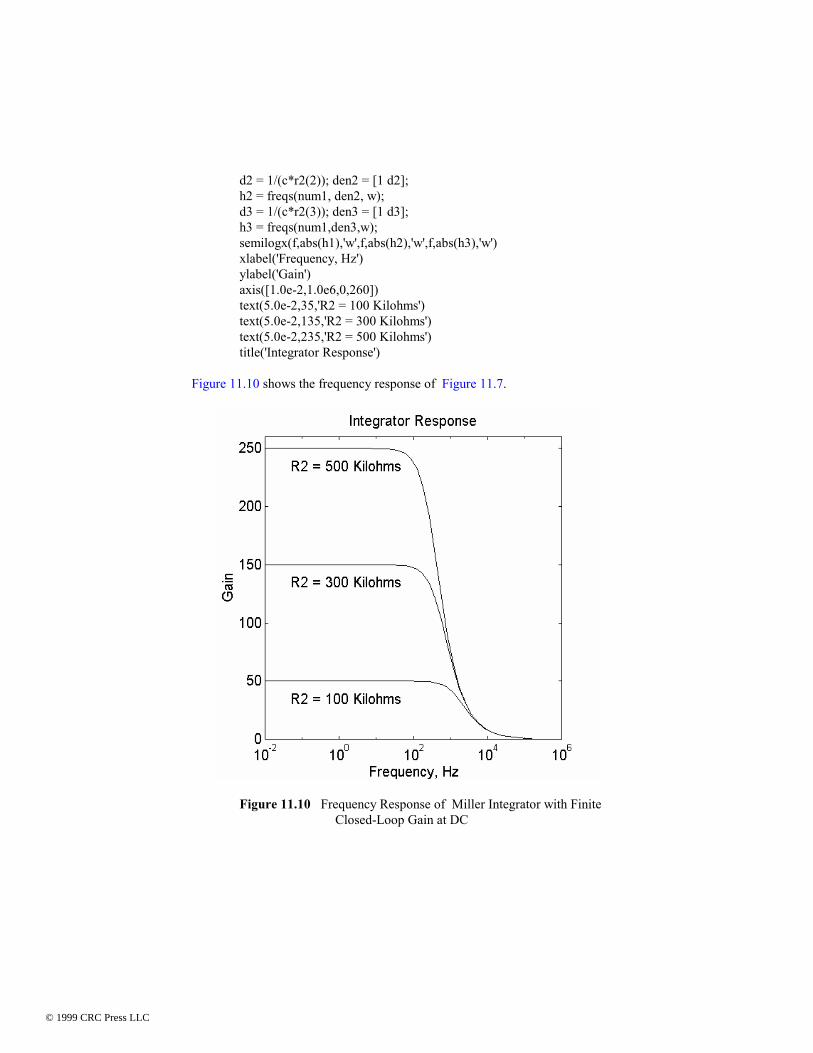
d2 = 1/(c*r2(2)); den2 = [1 d2]; h2 = freqs(num1, den2, w); d3 = 1/(c*r2(3)); den3 = [1 d3]; h3 = freqs(num1,den3,w); semilogx(f,abs(h1),'w',f,abs(h2),'w',f,abs(h3),'w') xlabel('Frequency, Hz') ylabel('Gain') axis([1.0e-2,1.0e6,0,260]) text(5.0e-2,35,'R2 = 100 Kilohms') text(5.0e-2,135,'R2 = 300 Kilohms') text(5.0e-2,235,'R2 = 500 Kilohms') title('Integrator Response')
Figure 11.10 shows the frequency response of Figure 11.7.
Figure 11.10 Frequency Response of Miller Integrator with Finite Closed-Loop Gain at DC
© 1999 CRC Press LLC
© 1999 CRC Press LLC
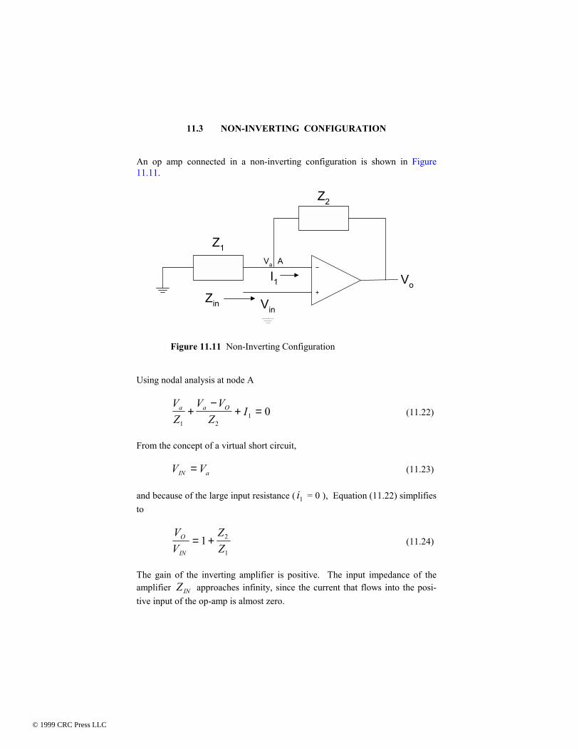
11.3 NON-INVERTING CONFIGURATION An op amp connected in a non-inverting configuration is shown in Figure 11.11.
Z2
Z1
I1 Vo
Va
VinZin
A
Figure 11.11 Non-Inverting Configuration Using nodal analysis at node A
VZ
V VZ
Ia a O
1 21 0+
−+ = (11.22)
From the concept of a virtual short circuit, V VIN a= (11.23) and because of the large input resistance ( i1 = 0 ), Equation (11.22) simplifies to
VV
ZZ
O
IN= +1 2
1 (11.24)
The gain of the inverting amplifier is positive. The input impedance of the amplifier ZIN approaches infinity, since the current that flows into the posi-tive input of the op-amp is almost zero.
© 1999 CRC Press LLC
© 1999 CRC Press LLC

If Z1 = R1 and Z2 = R2 , Figure 11.10 becomes a voltage follower with gain. This is shown in Figure 11.11.
VoVin
R2
R1
Figure 11.12 Voltage Follower with Gain The voltage gain is
VV
RR
O
IN= +
1 2
1 (11.25)
The zero, poles and the frequency response of a non-inverting configuration are obtained in Example 11.2. Example 11.2 For the Figure 11.13 (a) Derive the transfer function. (b) Use MATLAB to find the poles and zeros. ( c ) Plot the magnitude and phase response, assume that C1 = 0.1uF, C2 = 1000 0.1uF, R1 = 10KΩ, and R2 = 10 Ω.
VoVin
R2
R1
V1
C1
C2
Figure 11.13 Non-inverting Configuration
© 1999 CRC Press LLC
© 1999 CRC Press LLC
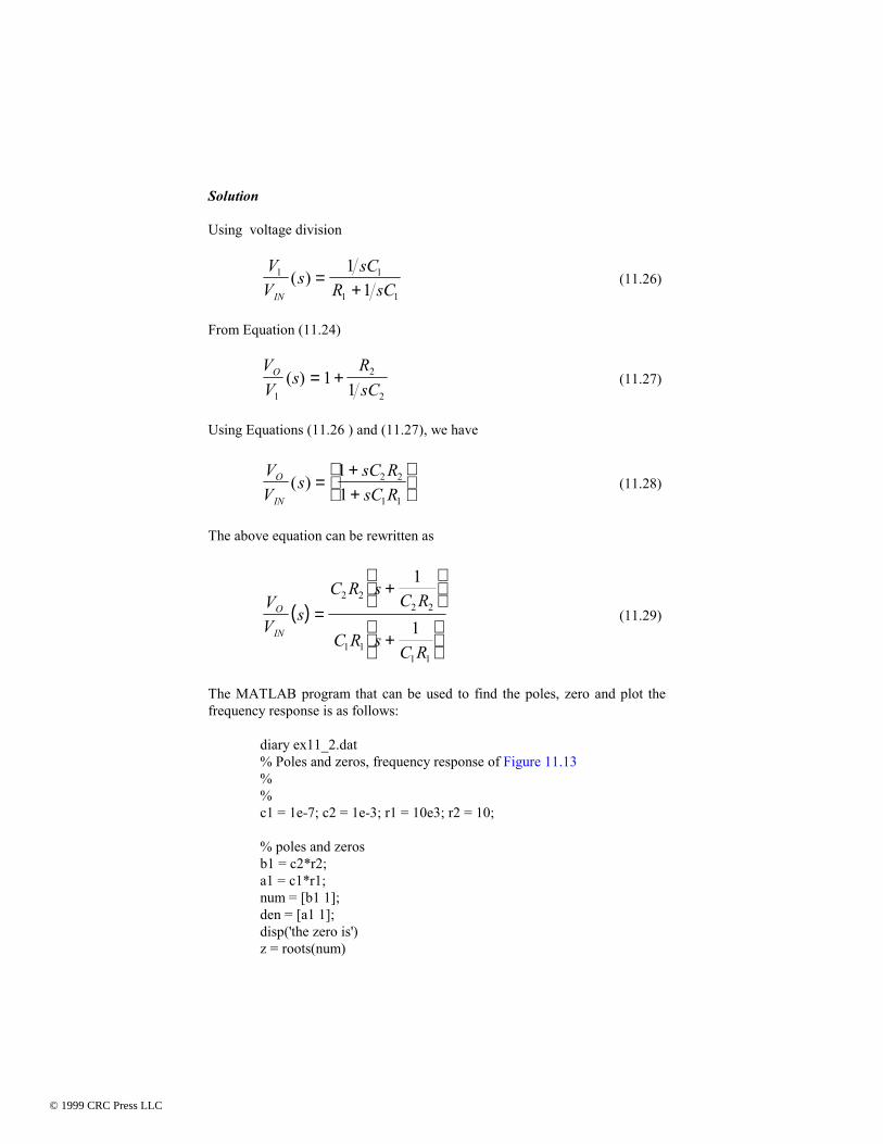
Solution Using voltage division
V
Vs
sCR sCIN
1 1
1 1
11
( ) =+
(11.26)
From Equation (11.24)
VV
sRsC
O
1
2
21
1( ) = + (11.27)
Using Equations (11.26 ) and (11.27), we have
VV
ssC RsC R
O
IN( ) =
++
11
2 2
1 1 (11.28)
The above equation can be rewritten as
( )VV
sC R s
C R
C R sC R
O
IN=
+
+
2 22 2
1 11 1
1
1 (11.29)
The MATLAB program that can be used to find the poles, zero and plot the frequency response is as follows:
diary ex11_2.dat % Poles and zeros, frequency response of Figure 11.13 % % c1 = 1e-7; c2 = 1e-3; r1 = 10e3; r2 = 10; % poles and zeros b1 = c2*r2; a1 = c1*r1; num = [b1 1]; den = [a1 1]; disp('the zero is') z = roots(num)
© 1999 CRC Press LLC
© 1999 CRC Press LLC
disp('the poles are') p = roots(den) % the frequency response w = logspace(-2,6); h = freqs(num,den,w); gain = 20*log10(abs(h)); f = w/(2*pi); phase = angle(h)*180/pi; subplot(211),semilogx(f,gain,'w'); xlabel('Frequency, Hz') ylabel('Gain, dB') axis([1.0e-2,1.0e6,0,22]) text(2.0e-2,15,'Magnitude Response') subplot(212),semilogx(f,phase,'w') xlabel('Frequency, Hz') ylabel('Phase') axis([1.0e-2,1.0e6,0,75]) text(2.0e-2,60,'Phase Response') diary
The results are:
the zero is z = -100
the pole is
p = -1000
The magnitude and phase plots are shown in Figure 11.14
© 1999 CRC Press LLC
© 1999 CRC Press LLC
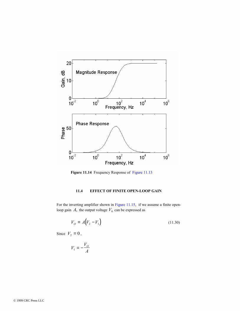
Figure 11.14 Frequency Response of Figure 11.13
11.4 EFFECT OF FINITE OPEN-LOOP GAIN For the inverting amplifier shown in Figure 11.15, if we assume a finite open-loop gain A, the output voltage V0 can be expressed as
( )V A V VO = −2 1 (11.30) Since V2 0= ,
VVAO
1 = −
© 1999 CRC Press LLC
© 1999 CRC Press LLC
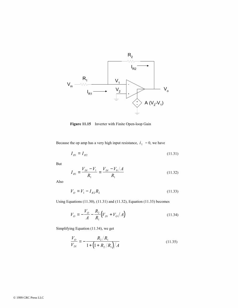
Vo
Vin
R2
R1
IR1
IR2
A (V2-V1)
V1
V2
Figure 11.15 Inverter with Finite Open-loop Gain Because the op amp has a very high input resistance, i 1 = 0, we have I IR R1 2= (11.31) But
IV V
RRIN
11
1=
−=
−V V AR
IN 0
1 (11.32)
Also V V I RO R= −1 2 2 (11.33) Using Equations (11.30), (11.31) and (11.32), Equation (11.33) becomes
( )VVA
RR
V V AOO
IN O= − − +2
1 (11.34)
Simplifying Equation (11.34), we get
( )VV
R RR R A
O
IN= −
+ +2 1
2 11 1 (11.35)
© 1999 CRC Press LLC
© 1999 CRC Press LLC
It should be noted that as the open-loop gain approaches infinity, the closed-loop gain becomes
VV
RR
O
IN≅ − 2
1
The above expression is identical to Equation (11.7). In addition, from Equation (11.30) , the voltage V1 goes to zero as the open-loop gain goes to infinity. Furthermore, to minimize the dependence of the closed-loop gain on the value of the open-loop gain, A, we should make
1 2
1+
<<
RR
A (11.36)
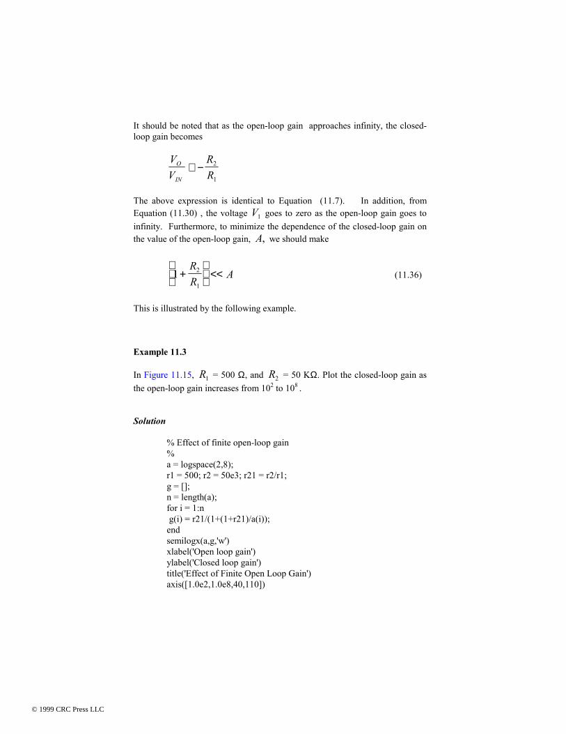
This is illustrated by the following example. Example 11.3 In Figure 11.15, R1 = 500 Ω, and R2 = 50 KΩ. Plot the closed-loop gain as the open-loop gain increases from 102 to 108 . Solution
% Effect of finite open-loop gain % a = logspace(2,8); r1 = 500; r2 = 50e3; r21 = r2/r1; g = []; n = length(a); for i = 1:n g(i) = r21/(1+(1+r21)/a(i)); end semilogx(a,g,'w') xlabel('Open loop gain') ylabel('Closed loop gain') title('Effect of Finite Open Loop Gain') axis([1.0e2,1.0e8,40,110])
© 1999 CRC Press LLC
© 1999 CRC Press LLC
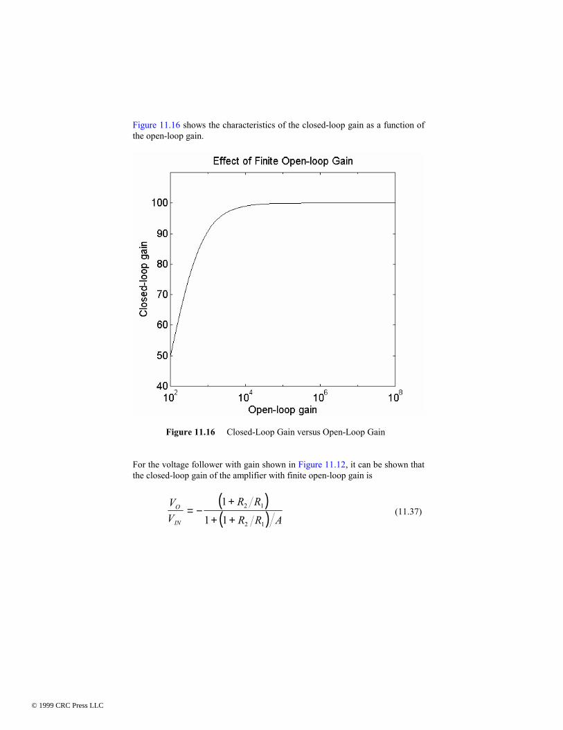
Figure 11.16 shows the characteristics of the closed-loop gain as a function of the open-loop gain.
Figure 11.16 Closed-Loop Gain versus Open-Loop Gain For the voltage follower with gain shown in Figure 11.12, it can be shown that the closed-loop gain of the amplifier with finite open-loop gain is
( )( )
VV
R R
R R AO
IN= −
+
+ +
1
1 12 1
2 1
(11.37)
© 1999 CRC Press LLC
© 1999 CRC Press LLC
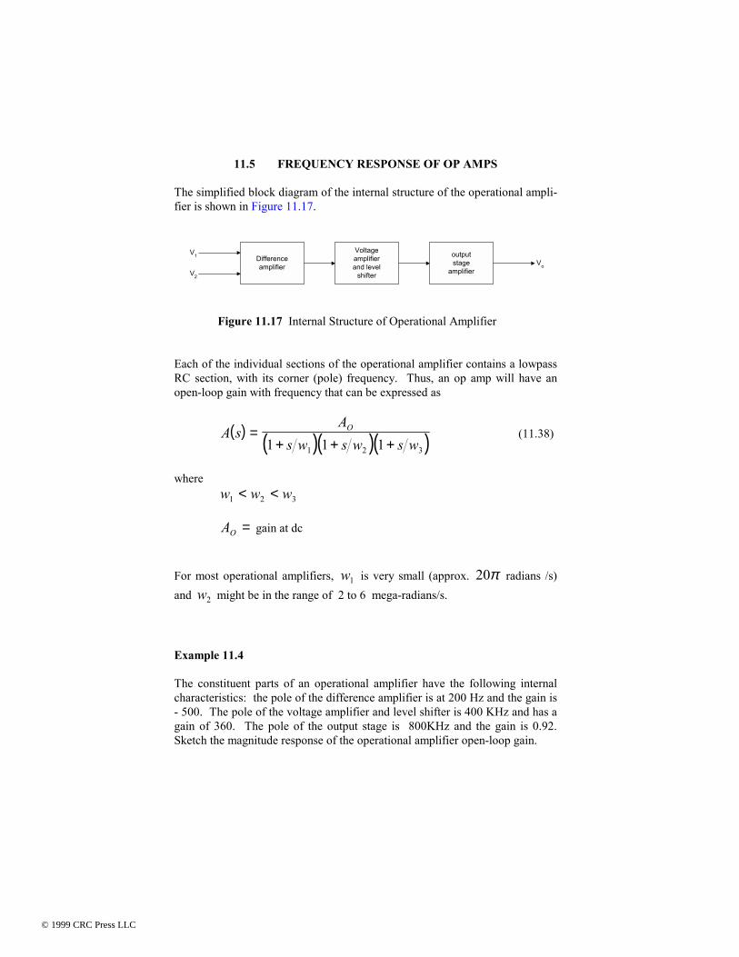
11.5 FREQUENCY RESPONSE OF OP AMPS The simplified block diagram of the internal structure of the operational ampli-fier is shown in Figure 11.17.
Vo
V1
V2
Differenceamplifier
Voltageamplifierand level
shifter
outputstage
amplifier
Figure 11.17 Internal Structure of Operational Amplifier Each of the individual sections of the operational amplifier contains a lowpass RC section, with its corner (pole) frequency. Thus, an op amp will have an open-loop gain with frequency that can be expressed as
( ) ( )( )( )A sA
s w s w s wO=
+ + +1 1 11 2 3
(11.38)
where w w w1 2 3< < AO = gain at dc For most operational amplifiers, w1 is very small (approx. 20π radians /s) and w2 might be in the range of 2 to 6 mega-radians/s. Example 11.4 The constituent parts of an operational amplifier have the following internal characteristics: the pole of the difference amplifier is at 200 Hz and the gain is - 500. The pole of the voltage amplifier and level shifter is 400 KHz and has a gain of 360. The pole of the output stage is 800KHz and the gain is 0.92. Sketch the magnitude response of the operational amplifier open-loop gain.
© 1999 CRC Press LLC
© 1999 CRC Press LLC
Solution The lowpass filter response can be expressed as
( )VV
jwC
jf fO
IN
rstage
p= −
+1 (11.39)
or
( )VV
sC
s wO
IN
rstage
p=
+1 (11.40)
The transfer function of the amplifier is given as
( ) ( ) ( ) ( )A ss s s
=−
+ + +500
1 400360
1 8 100 92
1 16 105 6π π π..
(11.41)
The above expression simplifies to
( )( )( )( )A s
xs s s
=+ + +
2 62 10400 8 10 16 10
21
5 6
..π π π
(11.42)
MATLAB script
% Frequency response of op amp % poles are p1 = 400*pi; p2 = 8e5*pi; p3 = 1.6e6*pi; p = [p1 p2 p3]; % zeros z = [0]; const = 2.62e21; % convert to poles and zeros and % find the frequency response a3 = 1; a2 = p1 + p2 + p3; a1 = p1*p2 + p1*p3 + p2*p3; a0 = p1*p2*p3; den = [a3 a2 a1 a0]; num = [const]; w = logspace(1,8);
© 1999 CRC Press LLC
© 1999 CRC Press LLC
h = freqs(num,den,w); f = w/(2*pi); g_db = 20*log10(abs(h)); % plot the magnitude response semilogx(f,g_db) title('Magnitude response') xlabel('Frequency, Hz') ylabel('Gain, dB')
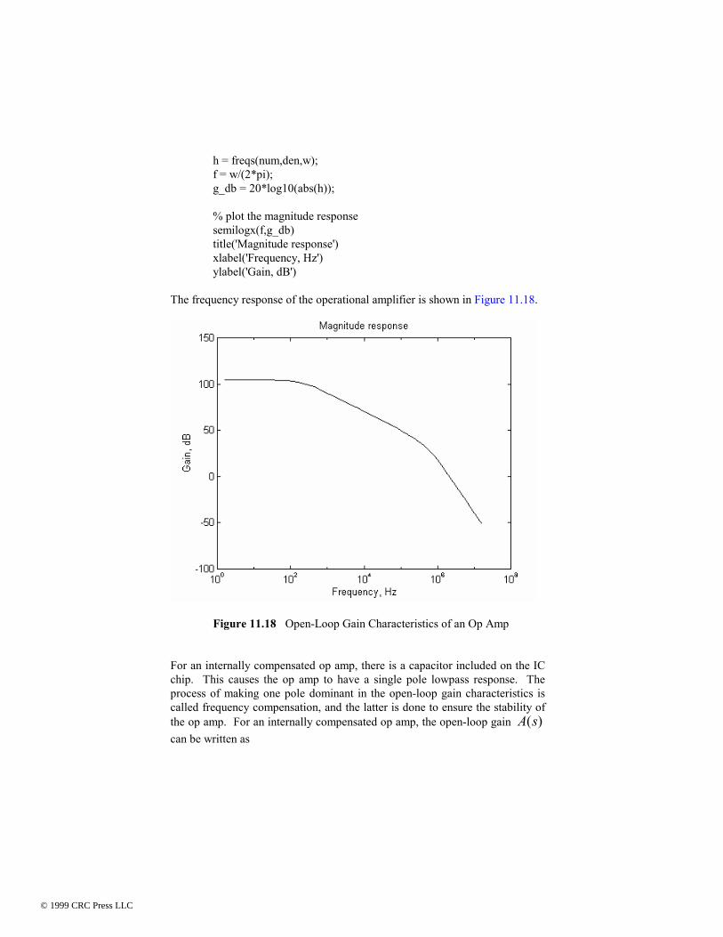
The frequency response of the operational amplifier is shown in Figure 11.18.
Figure 11.18 Open-Loop Gain Characteristics of an Op Amp For an internally compensated op amp, there is a capacitor included on the IC chip. This causes the op amp to have a single pole lowpass response. The process of making one pole dominant in the open-loop gain characteristics is called frequency compensation, and the latter is done to ensure the stability of the op amp. For an internally compensated op amp, the open-loop gain A s( ) can be written as
© 1999 CRC Press LLC
© 1999 CRC Press LLC
( ) ( )A sAs w
O
b
=+1
(11.43)
where
A0 is dc open-loop gain wb is break frequency. For the 741 op amp, A0 = 105 and wb = 20 π radians/s. At physical fre-quencies s jw= , Equation (11.43) becomes
( ) ( )A jwAjw w
O
b
=+1
(11.44)
For frequencies w > wb , Equation (11.44) can be approximated by
( )A jwA w
jwO b= (11.45)
The unity gain bandwidth, wt (the frequency at which the gain goes to unity), is given as
w A wt O b= (11.46) For the inverting amplifier shown in Figure 11.5, if we substitute Equation (11.43) into Equation (11.35), we get a closed-loop gain
( )( ) ( )
VV
sR R
R R As
w R R
O
INo
t
= −+ + +
+
2 1
2 12 1
1 11
(11.47)
In the case of non-inverting amplifier shown in Figure 11.12, if we substitute Equation (11.43) into Equation (11.37), we get the closed-loop gain expression
© 1999 CRC Press LLC
© 1999 CRC Press LLC
( )( ) ( )
VV
sR R
R R As
w R R
O
INo
t
=+
+ + ++
1
1 11
2 1
2 12 1
(11.48)
From Equations (11.47) and (11.48), it can be seen that the break frequency for the inverting and non-inverting amplifiers is given by the expression
wwR RdB
t3
2 11=
+ (11.49)
The following example illustrates the effect of the ratioRR
2
1 on the frequency
response of op amp circuits. Example 11.5 An op amp has an open-loop dc gain of 107 , the unity gain bandwidth of
108 Hz. For an op amp connected in an inverting configuration (Figure 11.5), plot the magnitude response of the closed-loop gain.
if RR
2
1 = 100 , 600, 1100
Solution Equation (11.47) can be written as
VV
s
w R
R RR
swA
wR
R
o
IN
t
t t( )
( )
( )
=+
+ ++
2
12
1
0 2
1
1
1
(11.50)
MATLAB script
% Inverter closed-loop gain versus frequency w = logspace(-2,10); f = w/(2*pi); r12 = [100 600 1100];
© 1999 CRC Press LLC
© 1999 CRC Press LLC
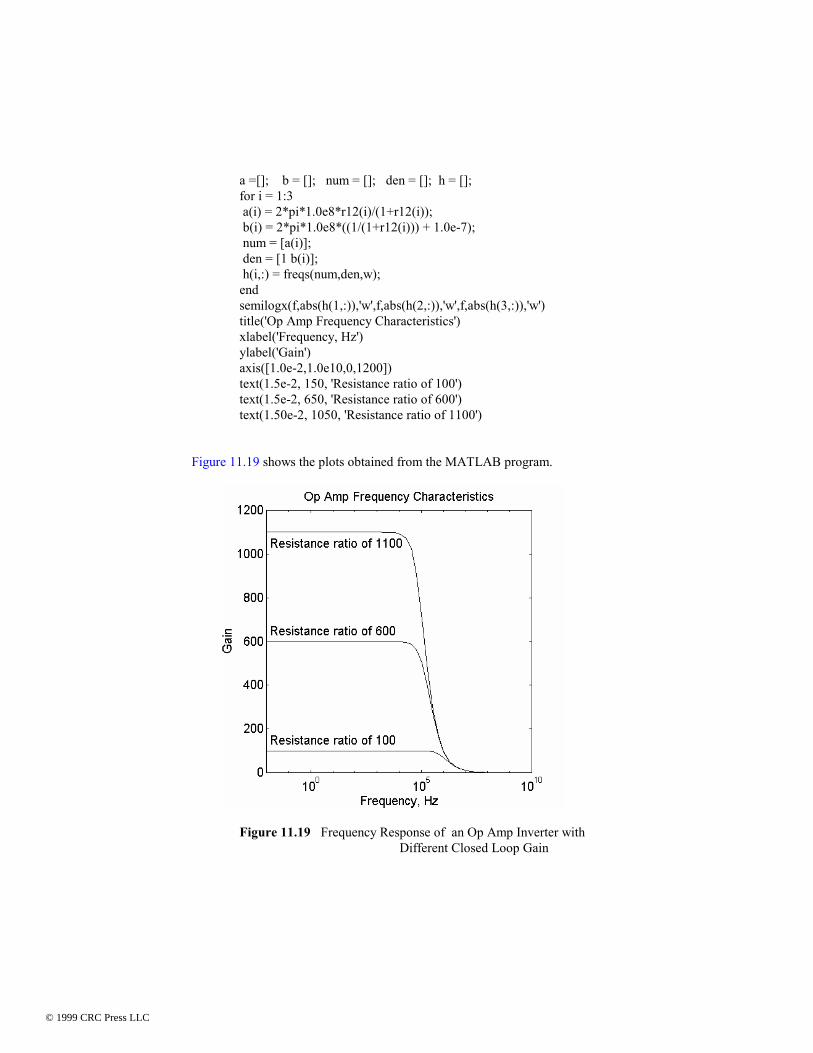
a =[]; b = []; num = []; den = []; h = []; for i = 1:3 a(i) = 2*pi*1.0e8*r12(i)/(1+r12(i)); b(i) = 2*pi*1.0e8*((1/(1+r12(i))) + 1.0e-7); num = [a(i)]; den = [1 b(i)]; h(i,:) = freqs(num,den,w); end semilogx(f,abs(h(1,:)),'w',f,abs(h(2,:)),'w',f,abs(h(3,:)),'w') title('Op Amp Frequency Characteristics') xlabel('Frequency, Hz') ylabel('Gain') axis([1.0e-2,1.0e10,0,1200]) text(1.5e-2, 150, 'Resistance ratio of 100') text(1.5e-2, 650, 'Resistance ratio of 600') text(1.50e-2, 1050, 'Resistance ratio of 1100')
Figure 11.19 shows the plots obtained from the MATLAB program.
Figure 11.19 Frequency Response of an Op Amp Inverter with
Different Closed Loop Gain
© 1999 CRC Press LLC
© 1999 CRC Press LLC
11.6 SLEW RATE AND FULL-POWER BANDWIDTH Slew rate (SR) is a measure of the maximum possible rate of change of the out-put voltage of an op amp. Mathematically, it is defined as
SRdVdt
O=max
(11.51)
The slew rate is often specified on the op amp data sheets in V/µs. Poor op amps might have slew rates around 1V/µs and good ones might have slew rates up to 1000 V/µs are available, but the good ones are relatively expensive. Slew rate is important when an output signal must follow a large input signal that is rapidly changing. If the slew rate is lower than the rate of change of the input signal, then the output voltage will be distorted. The output voltage will become triangular, and attenuated. However, if the slew rate is higher than the rate of change of the input signal, no distortion occurs and input and output of the op amp circuit will have similar wave shapes. As mentioned in the Section (11.5), frequency compensated op amp has an in-ternal capacitance that is used to produce a dominant pole. In addition, the op amp has a limited output current capability, due to the saturation of the input stage. If we designate Imax as the maximum possible current that is available to charge the internal capacitance of an op amp, the charge on the frequency-compensation capacitor is
CdV Idt= Thus, the highest possible rate of change of the output voltage is
SRdVdt
IC
O= =max
max (11.52)
For a sinusoidal input signal given by
( )v t V wti m= sin (11.53)
The rate of change of the input signal is
© 1999 CRC Press LLC
© 1999 CRC Press LLC
( )dv tdt
wV wtim= cos (11.54)
Assuming that the input signal is applied to a unity gain follower, then the out-put rate of change
( )dV
dtdv t
dtwV wtO i
m= = cos (11.55)
The maximum value of the rate of change of the output voltage occurs when cos( ) ,wt = 1 i.e., wt = 0 2 4, , . ...,π π the slew rate
SRdVdt
wVOm= =
max
(11.56)
Equation (11.56) can be used to define full-power bandwidth. The latter is the frequency at which a sinusoidal rated output signal begins to show distortion due to slew rate limiting. Thus
w V SRm o rated, = (11.57) Thus
fSRVm
o rated=
2π, , (11.58)
The full-power bandwidth can be traded for output rated voltage, thus, if the output rated voltage is reduced, the full-power bandwidth increases. The fol-lowing example illustrates the relationship between the rated output voltage and the full-power bandwidth.
Example 11.6 The LM 741 op amp has a slew rate of 0.5 V/µs. Plot the full-power band-width versus the rated output voltage if the latter varies from ± 1 to ± 10 V. Solution
% Slew rate and full-power bandwidth sr = 0.5e6;
© 1999 CRC Press LLC
© 1999 CRC Press LLC
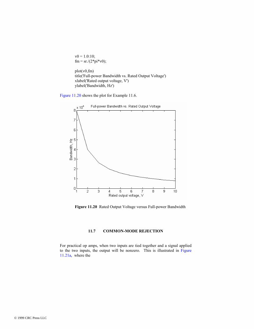
v0 = 1.0:10; fm = sr./(2*pi*v0); plot(v0,fm) title('Full-power Bandwidth vs. Rated Output Voltage') xlabel('Rated output voltage, V') ylabel('Bandwidth, Hz')
Figure 11.20 shows the plot for Example 11.6.
Figure 11.20 Rated Output Voltage versus Full-power Bandwidth
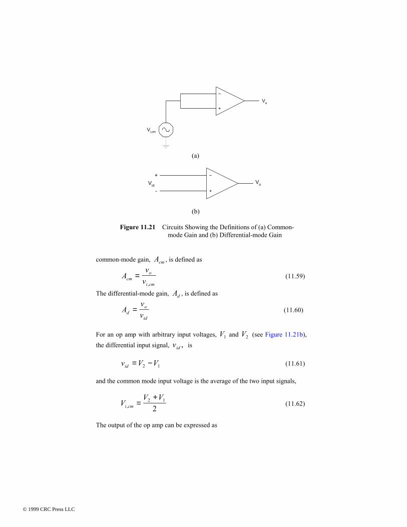
11.7 COMMON-MODE REJECTION For practical op amps, when two inputs are tied together and a signal applied to the two inputs, the output will be nonzero. This is illustrated in Figure 11.21a, where the
© 1999 CRC Press LLC
© 1999 CRC Press LLC
Vo
Vi,cm
(a)
Vo
+
-Vid
(b)
Figure 11.21 Circuits Showing the Definitions of (a) Common- mode Gain and (b) Differential-mode Gain
common-mode gain, Acm , is defined as
Av
vcmo
i cm=
, (11.59)
The differential-mode gain, Ad , is defined as
Avvd
o
id= (11.60)
For an op amp with arbitrary input voltages, V1 and V2 (see Figure 11.21b), the differential input signal, vid , is v V Vid = −2 1 (11.61) and the common mode input voltage is the average of the two input signals,
VV V
i cm, =+2 1
2 (11.62)
The output of the op amp can be expressed as
© 1999 CRC Press LLC
© 1999 CRC Press LLC
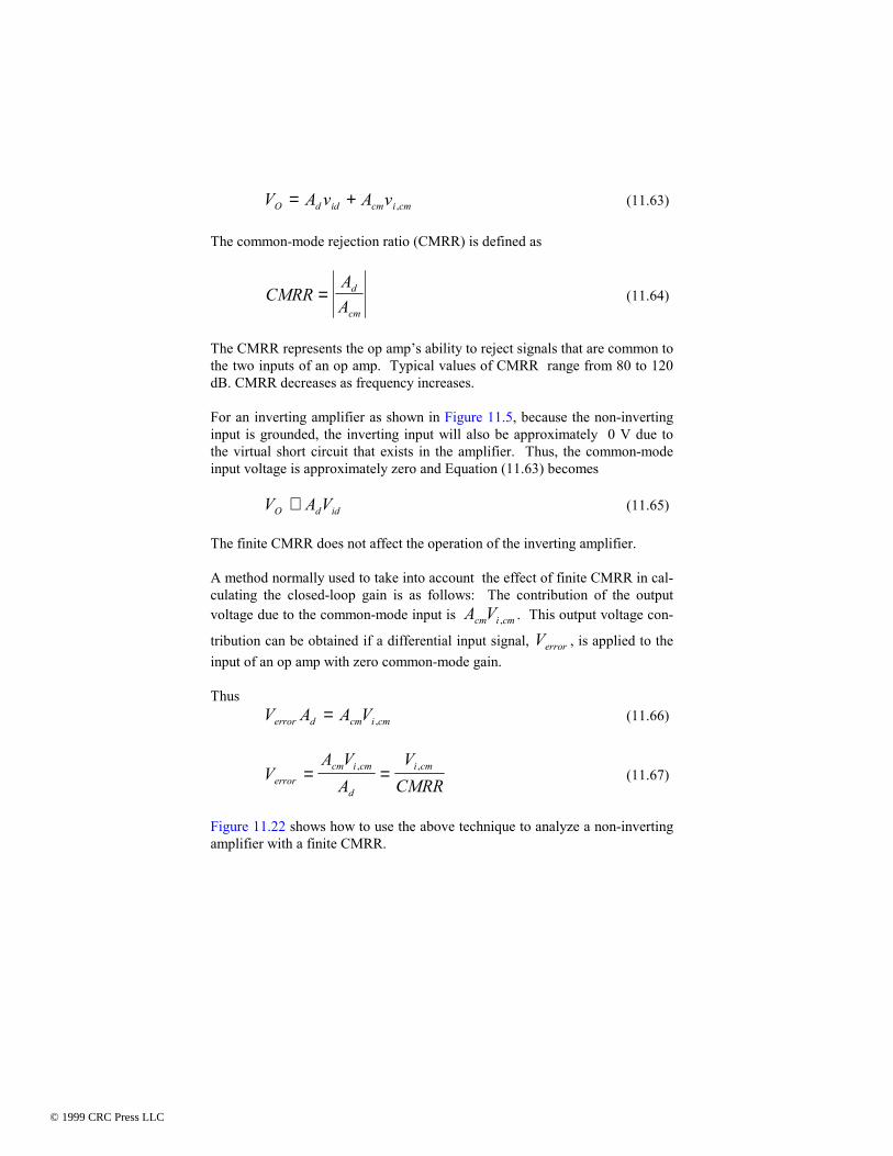
V A v A vO d id cm i cm= + , (11.63) The common-mode rejection ratio (CMRR) is defined as
CMRRAA
d
cm= (11.64)
The CMRR represents the op amp’s ability to reject signals that are common to the two inputs of an op amp. Typical values of CMRR range from 80 to 120 dB. CMRR decreases as frequency increases. For an inverting amplifier as shown in Figure 11.5, because the non-inverting input is grounded, the inverting input will also be approximately 0 V due to the virtual short circuit that exists in the amplifier. Thus, the common-mode input voltage is approximately zero and Equation (11.63) becomes V A VO d id≅ (11.65) The finite CMRR does not affect the operation of the inverting amplifier. A method normally used to take into account the effect of finite CMRR in cal-culating the closed-loop gain is as follows: The contribution of the output voltage due to the common-mode input is A Vcm i cm, . This output voltage con-
tribution can be obtained if a differential input signal, Verror , is applied to the input of an op amp with zero common-mode gain. Thus
V A A Verror d cm i cm= , (11.66)
VA V
AV
CMRRerrorcm i cm
d
i cm= =, , (11.67)
Figure 11.22 shows how to use the above technique to analyze a non-inverting amplifier with a finite CMRR.
© 1999 CRC Press LLC
© 1999 CRC Press LLC
Finite CMRR
Vo
R1
R2
Vi
(a)
Infinite CMRR
Vo
R1
R2
Verror
Vi
(b)
Figure 11.22 Non-inverting Amplifier (a) Finite CMRR ( b) Infinite CMRR
From Figure 11.22b, the output voltage is given as
( ) ( )V V R RV
CMRRR RO i
i= + + +1 12 1 2 1 (11.68)
The following example illustrates the effect of a finite CMRR on the closed-loop gain of a non-inverting amplifier.
© 1999 CRC Press LLC
© 1999 CRC Press LLC
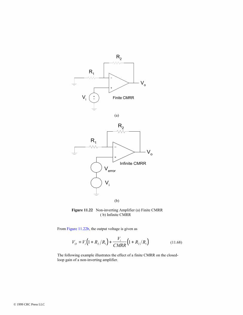
Example 11.7 For the amplifier shown in Figure 11.22, if R2 = 50KΩ and R1 = 1KΩ, plot the closed-loop gain versus CMRR for the following values of the latter: 10 10 10 10 104 5 6 7 8, , , , and 109.
Solution MATLAB Script
% Non-inverting amplifier with finite CMRR r2 = 50e3; r1 = 1.0e3; rr = r2/r1; cmrr = logspace(4,9,6); gain = (1+rr)*(1+1./cmrr); semilogx(cmrr,gain,'wo') xlabel('Common-mode Rejection Ratio') ylabel('Closed Loop Gain') title('Gain versus CMRR') axis([1.0e3,1.0e10,50.998, 51.008])
Figure 11.23 shows the effect of CMRR on the closed loop of a non-inverting amplifier.
Figure 11.23 Effect of finite CMRR on the Gain of a Non- inverting Amplifier
© 1999 CRC Press LLC
© 1999 CRC Press LLC
SELECTED BIBLIOGRAPHY 1. Schilling, D.L. and Belove, C., Electronic Circuits - Discrete and Integrated, 3rd Edition, McGraw Hill, 1989. 2. Wait, J.V., Huelsman, L.P., and Korn, G.A., Introduction to
Operational Amplifiers - Theory and Applications, 2nd Edition, McGraw Hill, 1992.
3. Sedra, A.S. and Smith, K.C., Microelectronics Circuits, 4th Edition, Oxford University Press, 1997. 4. Ferris, C.D., Elements of Electronic Design, West Publishing, 1995. 5. Irvine, R.G., Operational Amplifiers - Characteristics and Applications, Prentice Hall, 1981. 6. Ghausi, M.S., Electronic Devices and Circuits: Discrete and Integrated, HRW, 1985.
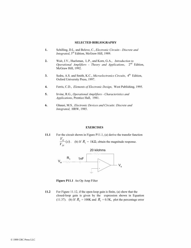
EXERCISES 11.1 For the circuit shown in Figure P11.1, (a) derive the transfer function
VV
sO
IN( ) . (b) If R1 = 1KΩ, obtain the magnitude response.
Vo
20 kilohms
R1 1nFVin
Figure P11.1 An Op Amp Filter 11.2 For Figure 11.12, if the open-loop gain is finite, (a) show that the
closed-loop gain is given by the expression shown in Equation (11.37). (b) If R2 = 100K and R1 = 0.5K, plot the percentage error
© 1999 CRC Press LLC
© 1999 CRC Press LLC

in the magnitude of the closed-loop gain for open-loop gains of 10 10 102 4 6, , and 108 .
11.3 Find the poles and zeros of the circuit shown in Figure P11.3. Use
MATLAB to plot the magnitude response. The resistance values are in kilohms.
Vo
10
1 nF
Vin
1 nF
1
Figure P11.3 An Op Amp Circuit 11.4 For the amplifier shown in Figure 11.12, if the open-loop gain is 106,
R2 = 24K, and R1 = 1K, plot the frequency response for a unity gain
bandwidth of 10 106 7, , and 108 Hz. 11.5 For the inverting amplifier, shown in Figure 11.5, plot the 3-dB
frequency versus resistance ratioRR
2
1 for the following values of the
resistance ratio: 10, 100, 1000, 10,000 and 100,000. Assume that AO = 106 and f t = 107 Hz.
11.6 For the inverting amplifier, shown in Figure 11.5, plot the closed
loop gain versus resistance ratio RR
2
1 for the following open-loop
gain, AO : 103, 105 and 107. Assume a unity gain bandwidth of
© 1999 CRC Press LLC
© 1999 CRC Press LLC
f t = 107 Hz and resistance ratio,RR
2
1 has the following values: 10,
100, 1000, 10,000 and 100,000. 11.7 An op amp with a slew rate of 1 V/µs is connected in the unity gain
follower configuration. A square wave of zero dc voltage and a peak voltage of 1 V and a frequency of 100 KHz is connected to the input of the unity gain follower. Write a MATLAB program to plot the output voltage of the amplifier.
11.8 For the non-inverting amplifier, if Ricm = 400 MΩ, Rid = 50 MΩ,
R1 = 2KΩ and R2 = 30KΩ, plot the input resistance versus the dc open-loop gain A0 . Assume the following values of the open-loop
gain: 10 10 103 5 7, , and 109 .
© 1999 CRC Press LLC
© 1999 CRC Press LLC


![Untitled-1 [] 2019/Fee_chart... · 2019-03-25 · IX = 4000 (Maths & English) X = 2800 (Maths) Maths & English) Amount (Maths & English) (Maths & English) Balance Fee Clerk's Sign](https://img.dokumen.tips/doc/110x75/5e6e31aa8f2b545f5d423876/untitled-1-2019feechart-2019-03-25-ix-4000-maths-english.jpg)